chapter 2 manufacturing process - ics.ee.nctu.edu.tmdker/courses/dic2005/chapter2(slchen).pdf ·...
TRANSCRIPT

EE1411Adapted from Digital Integrated Circuits 2nd
© 2003 Prentice Hall/Pearson Manufacturing
Digital Integrated Digital Integrated CircuitsCircuitsA Design PerspectiveA Design Perspective
Chapter 2 Chapter 2 ManufacturingManufacturingProcessProcess

EE1412Adapted from Digital Integrated Circuits 2nd
© 2003 Prentice Hall/Pearson Manufacturing
CMOS ProcessCMOS Process

EE1413Adapted from Digital Integrated Circuits 2nd
© 2003 Prentice Hall/Pearson Manufacturing
CMOS Process (nCMOS Process (n--well)well)Both NMOS and PMOS must be built in the same silicon
material.PMOS in n-wellNMOS in p-substrate

EE1414Adapted from Digital Integrated Circuits 2nd
© 2003 Prentice Hall/Pearson Manufacturing
A Modern CMOS ProcessA Modern CMOS Process
p-well n-well
p+
p-epi
SiO2
AlCu
poly
n+
SiO2
p+
gate-oxide
Tungsten
TiSi2
DualDual--Well TrenchWell Trench--Isolated CMOS ProcessIsolated CMOS Process
PMOS in n-wellNMOS in p-well

EE1415Adapted from Digital Integrated Circuits 2nd
© 2003 Prentice Hall/Pearson Manufacturing
Circuit Under DesignCircuit Under Design
VDD VDD
Vin Vout
M1
M2
M3
M4
Vout2

EE1416Adapted from Digital Integrated Circuits 2nd
© 2003 Prentice Hall/Pearson Manufacturing
Its Layout ViewIts Layout View

EE1417Adapted from Digital Integrated Circuits 2nd
© 2003 Prentice Hall/Pearson Manufacturing
The Manufacturing ProcessThe Manufacturing Process
•For a great tour through the IC manufacturing process and its different steps, checkhttp://www.fullman.com/semiconductors/semiconductors.html

EE1418Adapted from Digital Integrated Circuits 2nd
© 2003 Prentice Hall/Pearson Manufacturing
SiSilicon Waferlicon Wafer
A single crystal ingot cut into thin slices.Diameters: 4-12 inches

EE1419Adapted from Digital Integrated Circuits 2nd
© 2003 Prentice Hall/Pearson Manufacturing
oxidation
opticalmask
processstep
photoresist coatingphotoresistremoval (ashing)
spin, rinse, dryacid etch
photoresist
stepper exposure
development
Typical operations in a single photolithographic cycle (from [Fullman]).
PhotoPhoto--Lithographic ProcessLithographic Process

EE14110Adapted from Digital Integrated Circuits 2nd
© 2003 Prentice Hall/Pearson Manufacturing
PhotoPhoto--Lithographic Process (2)Lithographic Process (2)
Oxidation layering – this optional step deposits a thin layer of SiO2 over the complete wafer by exposing it to a mixture of high-purity oxygen and hydrogen at approximately 1000°C. The oxide is used as an insulation layer and also forms transistor gates.Photoresist coating – a light sensitive polymer is evenly applied to a thickness of approximately 1µm by spinning the wafer.
Positive photoresistNegative photoresist
Stepper exposure – a glass mask containing the patterns that we want to transfer to the silicon is brought in close proximity to the wafer.Photoresist development and bake – the wafer are developed in either an acid or base solution to remove the nonexposed areas of photoresist. Once the exposed photoresist is removed, the wafer is “soft baked” at a low temperature to harden the remaining photoresist.

EE14111Adapted from Digital Integrated Circuits 2nd
© 2003 Prentice Hall/Pearson Manufacturing
PhotoPhoto--Lithographic Process (3)Lithographic Process (3)
Acid etching – material is selectively removed from areas of the wafer that are not covered by photoresist.Spin, rinse, and dry – a special tool (called SRD) cleans the wafer with deionized water and dries it with nitrogen.Various process steps – ion implantation, plasma etching, metal deposition, and so on.Photoresist removal (or ashing) – a high-temperature plasma is used to selectively remove the remaining photoresist without damaging device layers.

EE14112Adapted from Digital Integrated Circuits 2nd
© 2003 Prentice Hall/Pearson Manufacturing
Patterning of SiO2Patterning of SiO2Si-substrate
Si-substrate Si-substrate
(a) Silicon base material
(b) After oxidation and depositionof negative photoresist
(c) Stepper exposure
PhotoresistSiO2
UV-lightPatternedoptical mask
Exposed resist
SiO2
Si-substrate
Si-substrate
Si-substrate
SiO2
SiO2
(d) After development and etching of resist,chemical or plasma etch of SiO 2
(e) After etching
(f) Final result after removal of resist
Hardened resist
Hardened resist
Chemical or plasmaetch

EE14113Adapted from Digital Integrated Circuits 2nd
© 2003 Prentice Hall/Pearson Manufacturing
Recurring Process Steps (1)Recurring Process Steps (1)Diffusion and Ion Implantation
Diffusion implantation: – The wafers are placed in a quartz tube embedded in a heated furnace. A gas
containing the dopant is introduced in the tube.– The dopants diffuse into the exposed surface both vertically and horizontally.
Ion implantation:– Dopants are introduced as ions into the material. The ion implantation system
directs and sweeps a beam of purified ions over the semiconductor surface.– Advantage:
It allows for an independent control of depth and dosage. – Disadvantage:
it damages the lattice of the semiconductor.
The annealing step, in which the wafer is heated to around 1000 °C for 15 to 30 minutes, and then allowed to cool slowly, is needed.

EE14114Adapted from Digital Integrated Circuits 2nd
© 2003 Prentice Hall/Pearson Manufacturing
Recurring Process Steps (2)Recurring Process Steps (2)Deposition
CMOS process requires the repetitive deposition of layers of a material over the complete wafer, to either act as buffers for a processing step, or as insulating or conducting layers.
Etching:Once a material has been deposited, etching is used selectively to form patterns such as wires, contact hole, and etc.Wet etching method etches material both vertically and horizontally, and dry etching method etches material only vertically.
Planarization:To reliably deposit a layer of material onto the semiconductor surface, it is essential that the surface be approximately flat.

EE14115Adapted from Digital Integrated Circuits 2nd
© 2003 Prentice Hall/Pearson Manufacturing
CMOS Process FlowCMOS Process FlowDefine active areas
Etch and fill trenches
Implant well regions
Deposit and patternpolysilicon layer
Implant source and drainregions and substrate contacts
Create contact and via windowsDeposit and pattern metal layers

EE14116Adapted from Digital Integrated Circuits 2nd
© 2003 Prentice Hall/Pearson Manufacturing
CMOS Process WalkCMOS Process Walk--Through (1)Through (1)
p+
p-epi (a) Base material: p+ substrate with p-epi layer
p+
(c) After plasma etch of insulatingtrenches using the inverse of the active area mask
p+
p-epi SiO2
Si3N4
(b) After deposition of gate-oxide andsacrificial nitride (acts as abuffer layer)

EE14117Adapted from Digital Integrated Circuits 2nd
© 2003 Prentice Hall/Pearson Manufacturing
CMOS Process WalkCMOS Process Walk--Through (2)Through (2)SiO2
(d) After trench filling, CMPplanarization, and removal of sacrificial nitride
(e) After n-well and VTp adjust implants
n
(f) After p-well andVTn adjust implants
p

EE14118Adapted from Digital Integrated Circuits 2nd
© 2003 Prentice Hall/Pearson Manufacturing
CMOS Process WalkCMOS Process Walk--Through (3)Through (3)
(g) After polysilicon depositionand etch
poly(silicon)
(h) After n+ source/drain andp+source/drain implants. These
p+n+
steps also dope the polysilicon.
(i) After deposition of SiO 2insulator and contact hole etch.
SiO2

EE14119Adapted from Digital Integrated Circuits 2nd
© 2003 Prentice Hall/Pearson Manufacturing
CMOS Process WalkCMOS Process Walk--Through (4)Through (4)
(j) After deposition and patterning of first Al layer.
Al
(k) After deposition of SiO 2insulator, etching of via’s,deposition and patterning ofsecond layer of Al.
AlSiO2

EE14120Adapted from Digital Integrated Circuits 2nd
© 2003 Prentice Hall/Pearson Manufacturing
Advanced MetallizationAdvanced Metallization

EE14121Adapted from Digital Integrated Circuits 2nd
© 2003 Prentice Hall/Pearson Manufacturing
Advanced MetallizationAdvanced Metallization

EE14122Adapted from Digital Integrated Circuits 2nd
© 2003 Prentice Hall/Pearson Manufacturing
Layout and Layout and Design RulesDesign Rules

EE14123Adapted from Digital Integrated Circuits 2nd
© 2003 Prentice Hall/Pearson Manufacturing
3D Perspective3D Perspective
Polysilicon Aluminum

EE14124Adapted from Digital Integrated Circuits 2nd
© 2003 Prentice Hall/Pearson Manufacturing
Design RulesDesign Rules
Interface between designer and process engineerGuidelines for constructing process masksUnit dimension: Minimum line widthDesign rules:
Width, Space, Clearance, Extension, and Overlap

EE14125Adapted from Digital Integrated Circuits 2nd
© 2003 Prentice Hall/Pearson Manufacturing
Design Rules Design Rules –– Width and SpaceWidth and Space
Width Space

EE14126Adapted from Digital Integrated Circuits 2nd
© 2003 Prentice Hall/Pearson Manufacturing
Design Rules Design Rules –– ClearanceClearance
Unrelated Related

EE14127Adapted from Digital Integrated Circuits 2nd
© 2003 Prentice Hall/Pearson Manufacturing
Design Rules Design Rules –– Extension and OverlapExtension and Overlap
Extension Overlap

EE14128Adapted from Digital Integrated Circuits 2nd
© 2003 Prentice Hall/Pearson Manufacturing
CMOS Process LayersCMOS Process LayersLayer
Polysilicon
Metal1
Metal2
Contact To Poly
Contact To Diffusion
Via
Well (p,n)
Active Area (n+,p+)
Color Representation
Yellow
Green
RedBlue
MagentaBlack
BlackBlack
Select (p+,n+) Green

EE14129Adapted from Digital Integrated Circuits 2nd
© 2003 Prentice Hall/Pearson Manufacturing
Layers in 0.25 Layers in 0.25 µµm CMOS processm CMOS process

EE14130Adapted from Digital Integrated Circuits 2nd
© 2003 Prentice Hall/Pearson Manufacturing
IntraIntra--Layer Design RulesLayer Design Rules
Metal2 4
3
10
90
Well
Active3
3
Polysilicon2
2
Different PotentialSame Potential
Metal1 3
32
Contactor Via
Select2
or6
2Hole

EE14131Adapted from Digital Integrated Circuits 2nd
© 2003 Prentice Hall/Pearson Manufacturing
Transistor LayoutTransistor Layout
1
2
5
3
Tran
sist
or
EE14132Adapted from Digital Integrated Circuits 2nd
© 2003 Prentice Hall/Pearson Manufacturing
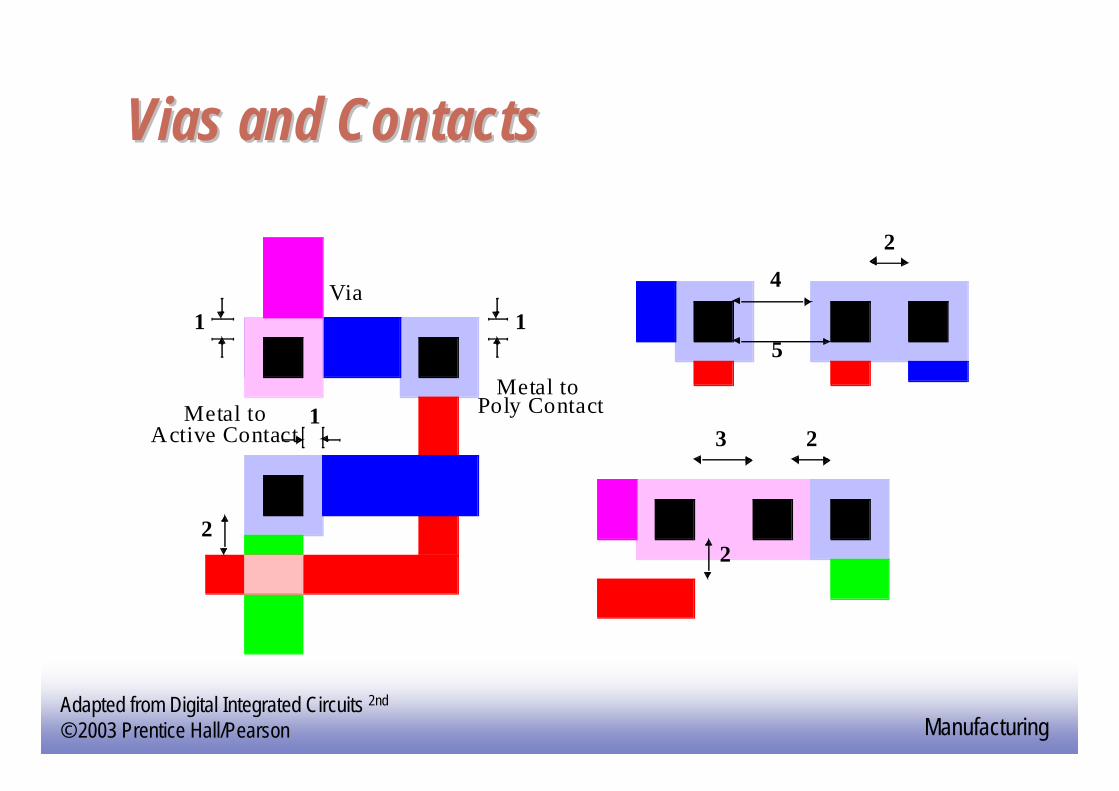
ViasVias and Contactsand Contacts
1
2
1
Via
Metal toPoly ContactMetal to
Active Contact
1
2
5
4
3 2
2

EE14133Adapted from Digital Integrated Circuits 2nd
© 2003 Prentice Hall/Pearson Manufacturing
Select LayerSelect Layer
1
3 3
2
2
2
WellSubstrate
Select3
5

EE14134Adapted from Digital Integrated Circuits 2nd
© 2003 Prentice Hall/Pearson Manufacturing
CMOS Inverter LayoutCMOS Inverter Layout
A A’
np-substrate Field
Oxidep+n+
In
Out
GND VD D
(a) Layout
(b) Cross-Section along A-A’
A A’

EE14135Adapted from Digital Integrated Circuits 2nd
© 2003 Prentice Hall/Pearson Manufacturing
Layout Editor Layout Editor -- maxmax
It is developed at the University of California at Berkeley.

EE14136Adapted from Digital Integrated Circuits 2nd
© 2003 Prentice Hall/Pearson Manufacturing
Layout Editor Layout Editor -- VirtuosoVirtuoso

EE14137Adapted from Digital Integrated Circuits 2nd
© 2003 Prentice Hall/Pearson Manufacturing
Layout Editor Layout Editor -- LakerLaker

EE14138Adapted from Digital Integrated Circuits 2nd
© 2003 Prentice Hall/Pearson Manufacturing
Design Rule CheckerDesign Rule CheckerDRC (Design Rule Check)
Using CAD tools to verify the layout
On-line DRC:Diva (Virtuoso)
Off-line DRC:Dracula

EE14139Adapted from Digital Integrated Circuits 2nd
© 2003 Prentice Hall/Pearson Manufacturing
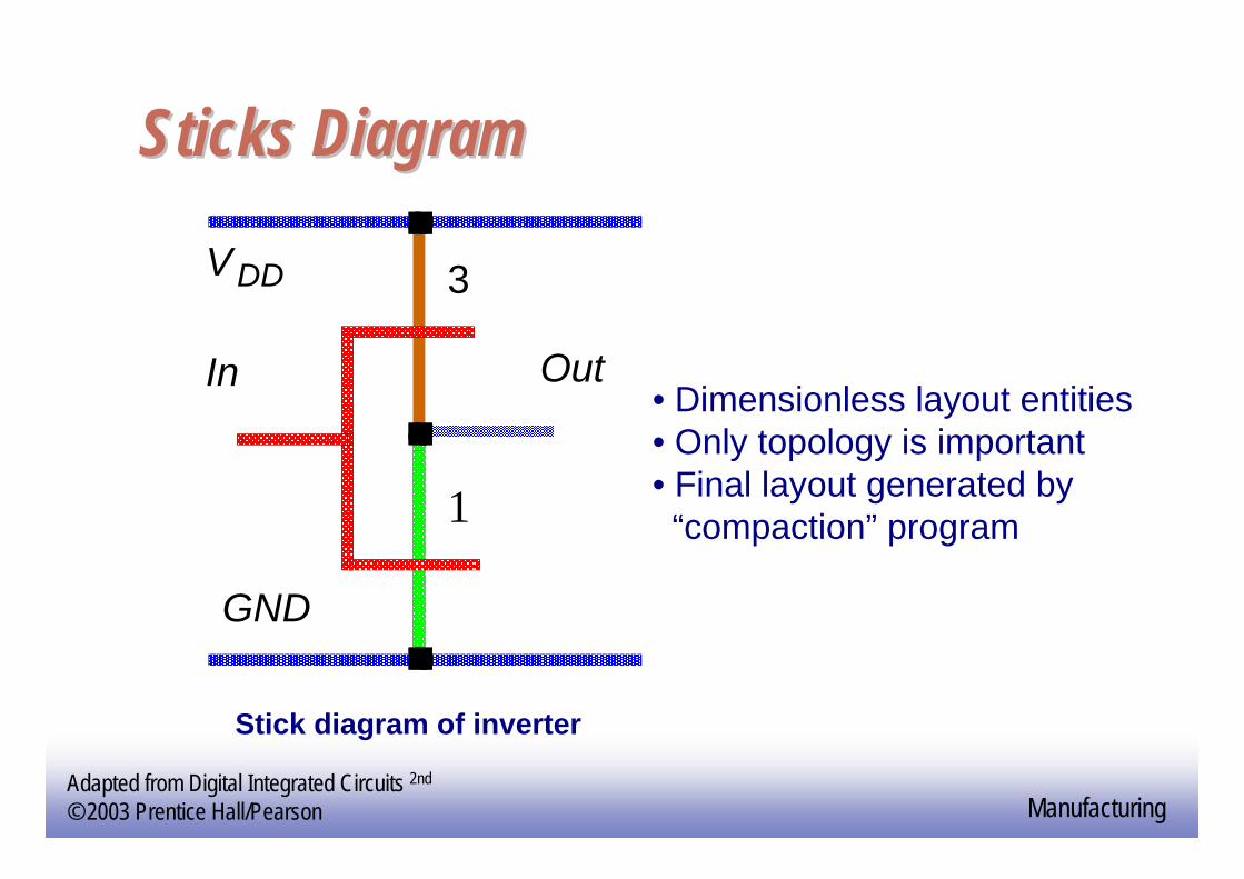
Symbolic LayoutSymbolic Layout
Full-custom VS Cell-BasedSymbolic Layout
The designer only draw a shorthand notation for the layout structure (transistors, contacts, wires).Advantage: designers don’t care design rulesDisadvantages: The density is unpredictable.
EE14140Adapted from Digital Integrated Circuits 2nd
© 2003 Prentice Hall/Pearson Manufacturing
Sticks DiagramSticks Diagram
1
3
In Out
VDD
GND
Stick diagram of inverter
• Dimensionless layout entities• Only topology is important• Final layout generated by “compaction” program

EE14141Adapted from Digital Integrated Circuits 2nd
© 2003 Prentice Hall/Pearson Manufacturing
Layout Example Layout Example -- InverterInverter

EE14142Adapted from Digital Integrated Circuits 2nd
© 2003 Prentice Hall/Pearson Manufacturing
Design Example Design Example -- NAND (1)NAND (1)

EE14143Adapted from Digital Integrated Circuits 2nd
© 2003 Prentice Hall/Pearson Manufacturing
Design Example Design Example –– NAND (2)NAND (2)

EE14144Adapted from Digital Integrated Circuits 2nd
© 2003 Prentice Hall/Pearson Manufacturing
PackagingPackaging

EE14145Adapted from Digital Integrated Circuits 2nd
© 2003 Prentice Hall/Pearson Manufacturing
Packaging RequirementsPackaging RequirementsRequirements
Electrical: Low parasiticsMechanical: Reliable and robustThermal: Efficient heat removal
– Commercial: 0~75 °C– Military: -55~125 °C
Economical: CheapMaterials
Plastics– Up to 2 W
Ceramic Al2O3 (Alumina)– Up to 20 W– Disadvantage:
High dielectric constant => Large interconnect capacitance

EE14146Adapted from Digital Integrated Circuits 2nd
© 2003 Prentice Hall/Pearson Manufacturing
Wire BondingWire Bonding
Wires materials: Aluminum or goldDisadvantages:
Longer manufacturingWire distanceHard to predict parasitics
Lead Frame
Substrate
Die
Pad

EE14147Adapted from Digital Integrated Circuits 2nd
© 2003 Prentice Hall/Pearson Manufacturing
TapeTape--Automated Bonding (TAB)Automated Bonding (TAB)
(a) Polymer Tape with imprinted
(b) Die attachment using solder bumps.
wiring pattern.
Substrate
Die
Solder BumpFilm + Pattern
Sprockethole
Polymer film
Leadframe
Testpads

EE14148Adapted from Digital Integrated Circuits 2nd
© 2003 Prentice Hall/Pearson Manufacturing
FlipFlip--Chip BondingChip Bonding
Solder bumps
Substrate
Die
Interconnect
layers

EE14149Adapted from Digital Integrated Circuits 2nd
© 2003 Prentice Hall/Pearson Manufacturing
PackagePackage--toto--Board InterconnectBoard Interconnect
(a) Through-Hole Mounting (b) Surface Mount

EE14150Adapted from Digital Integrated Circuits 2nd
© 2003 Prentice Hall/Pearson Manufacturing
Package TypesPackage Types1. Bare die2. DIP3. PGA4. Small-outline IC5. Quad flat pack6. PLCC7. Leadless carrier

EE14151Adapted from Digital Integrated Circuits 2nd
© 2003 Prentice Hall/Pearson Manufacturing
Package ParametersPackage Parameters
EE14152Adapted from Digital Integrated Circuits 2nd
© 2003 Prentice Hall/Pearson Manufacturing
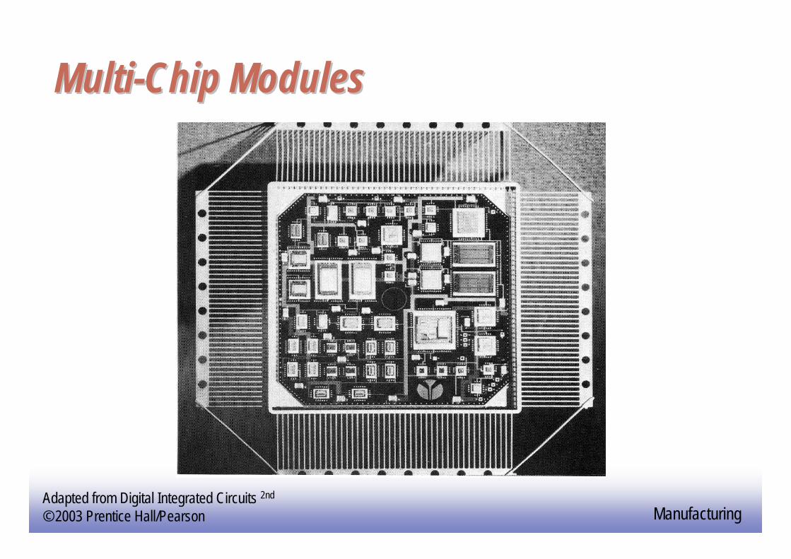
MultiMulti--Chip ModulesChip Modules

EE14153Adapted from Digital Integrated Circuits 2nd
© 2003 Prentice Hall/Pearson Manufacturing
Trend in ProcessTrend in Process
Now:LDD (Lightly Doped Drain)Silicide
Short-Term Copper and Low-k DilectricSOI (Silicon on Insulator)
Long-Term3-D integrated circuits