chapter 2 pwm and psm dc/dc buck...
TRANSCRIPT

18
CHAPTER 2
PWM AND PSM DC/DC BUCK CONVERTERS
PWM (Erickson 1997) and PSM (Ping Luo et al 2006)
DC–DC converters are categories of switching-mode voltage regulators. In
these types of converters, transistors are operated as switches in saturation or
cut-off regions, which dissipate much less power than that of linear
regulators. The controllers suitably driving the switches based on the error
between feedback and reference values effect voltage regulation. This chapter
includes modeling and simulation of PWM and PSM buck converters. Circuit
operation, modeling and simulation of PWM converter is included in
section 2.1 and that of PSM converter in section 2.2. Results of observations
on the non-linear phenomena of respective converters are included at the end
of each section.
2.1 PWM DC DC BUCK CONVERTER
A PWM dc–dc buck converter circuit in Figure 2.1 consists of a
controllable switch S, a freewheeling diode, an inductor L, and a filter
capacitor C. Resistor R represents a dc load. Power MOSFETs are preferred
as controllable switches due to their high switching speeds. DC power source
at the input is often an unregulated varying voltage source. Switch is driven
from a PWM controller designed to modify the switching duration to control
the output voltage. Diode is chosen to be a fast recovery or Schottky type.

19
Figure 2.1 PWM Buck converter
2.1.1 Circuit Operation
MOSFET switch, which is controlled by a PWM controller, is
turned ON and OFF at a predetermined frequency. This results in the DC
input voltage chopped and presented as a rectangular wave to the filter stage.
LC filter smoothes out the ripple and the average output voltage v0 at steady
state is given by v0=dVin.
Output voltage is controlled by suitably modulating the pulse width
or TON duration in PWM control. Sample of the output voltage is compared
with reference voltage and the error voltage after due compensation is
compared with a switching frequency saw tooth wave. The comparator output
L
C
+
-
Vin
R
MOSFET
PWM CONTROLLER

20
drives the switch and controls the output by suitably modifying the pulse
width or TON. Voltage fed to the LC filter due to switching operation is as
shown in Figure 2.2.
Figure 2.2 Input voltage presented to LC filter due to switch action
An ideal filter results in ripple free output voltage with 100%
efficient converter assuming that the switches are also ideal. LC filter is so
designed that its cut-off frequency is well below the switching frequency so
that the switching frequency components are not passed to the output with
significant amplitude. Voltage across C and inductor current are shown in
Figure 2.3. A practical switching converter, even though superior in
efficiency to linear converters, has output voltage with ripple and poor in
response.
Time in mS
Vol
tage
inV

21
Figure 2.3 Typical waveforms of inductor current iL and capacitor voltage vC
2.1.2 Operating Modes of Converter
The converter can operate in two distinct modes namely
Continuous Conduction Mode (CCM) and DCM (Erickson and Maksimovic
2000). Under CCM the inductor current iL is always greater than zero and is
never discontinuous. Hence every cycle starts with a nonzero inductor
current. In the case of DCM the inductor current becomes zero before the
switch is closed for next cycle.
Hence in the case of DCM operation every cycle starts from a zero
inductor current after a brief period over which the inductor current was zero
within the previous cycle. The converter can also operate in critical mode at
the border with inductor current zero just becoming zero for an instant of time
and this duration over which the current was zero can be taken to be zero.
This mode is also known as Border Conduction Mode or Boundary
Conduction Mode (Basso 2008).
Time in mS
iLin
Aan
dvC
inV
i Lin
Aan
dv C
inV
22
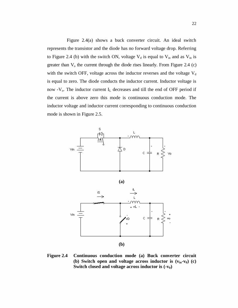
Figure 2.4(a) shows a buck converter circuit. An ideal switch
represents the transistor and the diode has no forward voltage drop. Referring
to Figure 2.4 (b) with the switch ON, voltage Vd is equal to Vin and as Vin is
greater than Vo the current through the diode rises linearly. From Figure 2.4 (c)
with the switch OFF, voltage across the inductor reverses and the voltage Vd
is equal to zero. The diode conducts the inductor current. Inductor voltage is
now -Vo. The inductor current IL decreases and till the end of OFF period if
the current is above zero this mode is continuous conduction mode. The
inductor voltage and inductor current corresponding to continuous conduction
mode is shown in Figure 2.5.
(a)
(b)
Figure 2.4 Continuous conduction mode (a) Buck converter circuit (b) Switch open and voltage across inductor is (vin-v0) (c) Switch closed and voltage across inductor is (-v0)
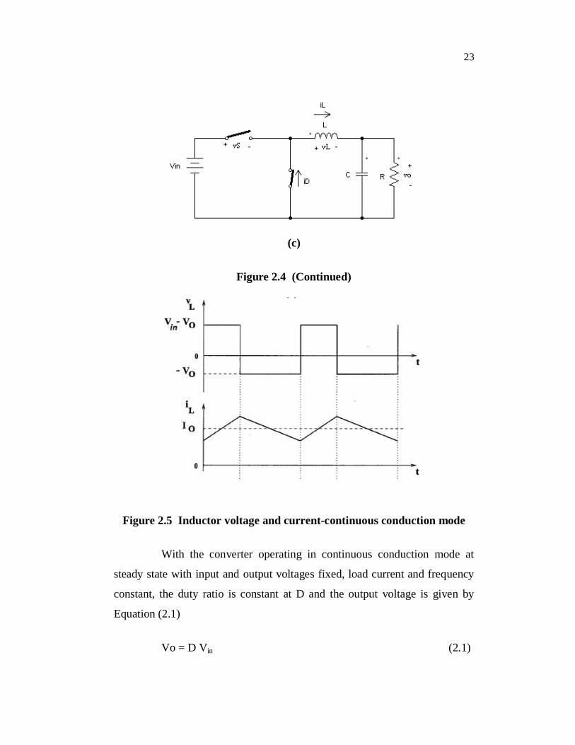
23
(c)
Figure 2.4 (Continued)
Figure 2.5 Inductor voltage and current-continuous conduction mode
With the converter operating in continuous conduction mode at
steady state with input and output voltages fixed, load current and frequency
constant, the duty ratio is constant at D and the output voltage is given by
Equation (2.1)
Vo = D Vin (2.1)

24
where,
V0 – Output voltage
Vin – Input voltage
D– Duty cycle
TTD ON (2.2)
swOFFON f
TTT 1 (2.3)
ONT – ON state duration (S)
OFFT – OFF state duration (S)
T – Total duration (S)
swf – Switching frequency (Hz)
During the TOFF period if the inductor current falls to zero for a
portion of the switching cycle as shown in Figure 2.6 the converter is said to
be in discontinuous conduction mode. The current starts at zero, reaches a
peak value, and returns to zero during each switching cycle. The circuit takes
up a third configuration as shown in Figure 2.7.
Figure 2.6 Inductor current - Discontinuous conduction mode

25
Figure 2.7 Third circuit configuration- Discontinuous conduction mode
With the converter operating in continuous conduction mode at
steady state with input and output voltages fixed, load current and frequency
constant, the duty ratio is constant at D and the output voltage is given by
Equation (2.4)
in
in
TVDLI
VV2
00 21
(2.4)
where I0 – output current
Modeling of voltage mode controlled buck converter
A switching converter model is useful to study how the input
voltage, load current, or the duty cycle variations affect the output voltage.
The switching buck converter switching between two time-invariant systems
during each switching period under continuous conduction mode is actually a
time- variant system due to the switching action. It is possible to approximate
this time-variant system with a linear time-invariant continuous-time system
using State-space averaging technique (Middlebrook and Cuk 1977).
A buck converter is modelled using state space averaging (Forsyth
and Mollov 1998) and simulated using MATLAB/SIMULINK. Model

26
considers the ESR of the capacitor and diode forward drop and neglects the
inductor series resistance. Regulation is effected through voltage mode
control and analysed for performance and exhibition of nonlinear phenomena
with input voltage as parameter.
State space averaged model for buck converter:
When two or more than two sets of state equations each describing
a state of the circuit due to action of switches are available then these state
equations can be averaged over the switching period by dividing the weighted
sum with the period.
In the converter studied under continuous conduction mode there
are two sets of equations available, with one set for switch closed and one set
for the switch open. These state equations are averaged over the switching
period.
A buck converter is modelled with diode forward drop and ESR of
filter capacitor considered. State equations are developed by applying KVL
and KCL to each of the two circuits and averaged.
Figure 2.8 Buck converter circuit
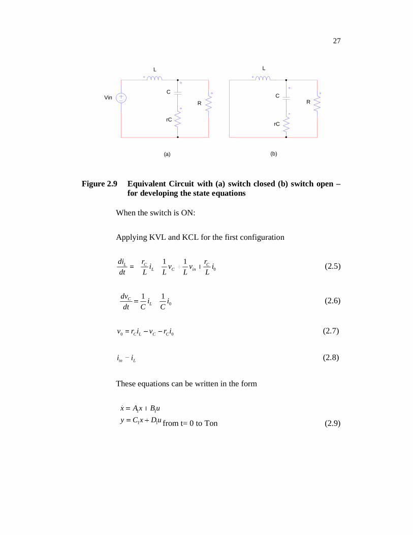
27
Figure 2.9 Equivalent Circuit with (a) switch closed (b) switch open – for developing the state equations
When the switch is ON:
Applying KVL and KCL for the first configuration
011 i
Lrv
Lv
Li
Lr
dtdi C
inCLCL (2.5)
011 iC
iCdt
dvL
C (2.6)
00 irvirv CCLC (2.7)
Lin ii (2.8)
These equations can be written in the form
uDxCyuBxAx
11
11
from t= 0 to Ton (2.9)
Vin
L
C
R
L
CR
rCrC
(a) (b)

28
When the switch is OFF:
Applying KVL and KCL for the second configuration
011 i
Lrv
Lv
Li
Lr
dtdi C
dCLCL
(2.10)
011 iC
iCdt
dvL
C
(2.11)
00 irvirv CCLC (2.12)
0ini (2.13)
uDxCyuBxAx
22
22 from t = Ton to T, over a duration of (1-d)T ( 2.14)
Averaged state space equations with duty ratio d are
011 i
Lrv
Ldv
Ldv
Li
Lr
dtdi C
dinCLCL (2.15)
011 iC
iCdt
dvL
C (2.16)
00 irvirv CCLC (2.17)
Lin dii (2.18)
The averaged state space equations are
DuCxyBuAxx
(2.19)

29
where
21 1 AddAA (2.20)
21 1 BddBB (2.21)
By linearising the above equations, the small signal representation
can be got. In the state space form
uBxAx (2.22)
uDxCy (2.23)
TCL vix (2.24)
Tin divu 0 (2.25)
Tin viy 0 (2.26)
0C1
L1-
Lr
AC
(2.27)
010C
LVV
Lr
LD
BdinC
(2.28)
10 CrDC (2.29)
0000
C
L
ri
D (2.30)
30
TCL vix and
Tin divu 0 are inductor current, capacitor
voltage, input voltage, output current and duty cycle perturbations.
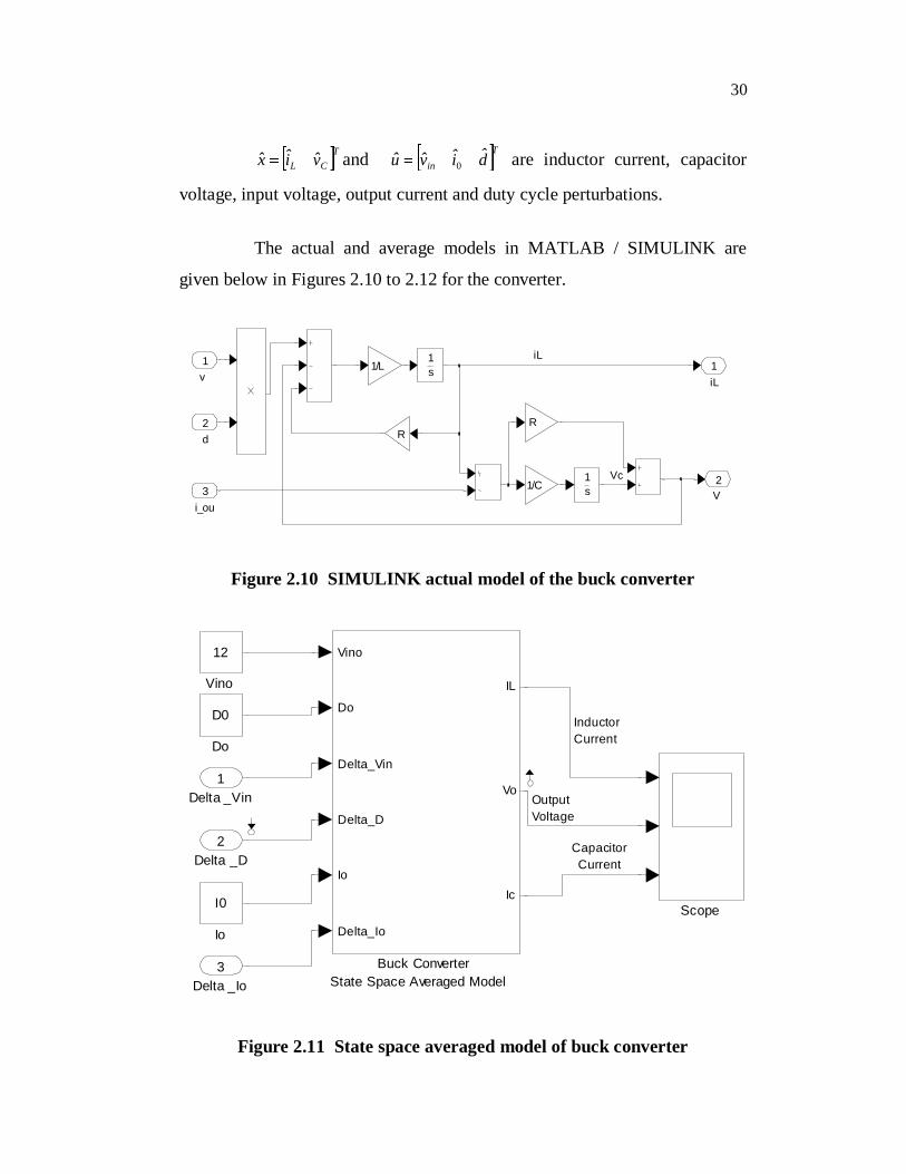
The actual and average models in MATLAB / SIMULINK are
given below in Figures 2.10 to 2.12 for the converter.
iL
Vc
V2
iL1
1s
1s
R
1/C
RL
1/L
i_out
3
d2
v1
Figure 2.10 SIMULINK actual model of the buck converter
Figure 2.11 State space averaged model of buck converter
Vino
12
Scope
Io
I0
Do
D0
Buck ConverterState Space Averaged Model
Vino
Do
Delta_Vin
Delta_D
Io
Delta_Io
IL
Vo
Ic
Delta _Io3
Delta _D2
Delta _Vin1
OutputVoltage
InductorCurrent
CapacitorCurrent

31
Figure 2.12 Simulink PSB model of converter
2.1.3 Voltage Mode Controlled Buck Converter
Voltage-mode controller is a type of fixed-frequency PWM
controller. It consists of a clock generator corresponding to the switching
frequency, a voltage error amplifier with compensator that generates control
voltage, a ramp generator operating in synchronism with the clock, and a
comparator to compare the control voltage with the sawtooth signal. The
output of the comparator is used to drive the controlled switch.
Buck converter with PWM voltage mode control is shown in
Fig.2.13. Output voltage is sensed with a voltage sensor, with a sensor gain,
which may be a voltage divider consisting of precision resistors suitably
selected for the available reference voltage. The output voltage signal is
compared with the reference voltage. If the output voltage is lower than the
desired value, a positive error voltage is produced. The compensator
processes the error voltage and the control voltage is produced with a d,
which is positive in this case, and the duty cycle is increased. This increases
the output voltage.
duty ratio
D
v+-
Scope 1
PWM block
d c g
DS
Diode
i+ -

32
The stability and transient response depend on the compensator
circuit. Figure 2.14 shows the overall transfer function block diagram with
input voltage and load current as disturbances.
Figure 2.13 Voltage mode controlled PWM Buck converter
Figure 2.14 Closed loop with compensator
Vcon
gain
gain
GAIN & Gc
40kHz
V15/8V
D
Comp
+
-
Vref
Comp
L
C
+
-
Vin
MOSFET
R

33
The transfer function of the PWM generator is basically 1/VM,
where VM is the peak to peak voltage of ramp given by (VU-VL) where VU is
the peak value and VL is the valley as shown.
Figure 2.15 PWM generation
The transfer function of the buck converter and PWM is:
1
112
RLCrsLCs
VCsrV
)s(GC
inC
M
(2.31)
A compensator can be designed that improves phase margin and
static gains to better the performance. For voltage mode control feedback the
compensator gain is Gc.
For a closed loop system:
The loop gain T(s) = H(s)Gc(s)Gvd(s)/Vm (2.32)
Then input voltage disturbance to output transfer function is

34
sT
svG
sinvsv in
oi
refv 10
0 (2.33)
Load current disturbance to output voltage transfer function is
sT
sZ
sisv
inv
refv 10
00
0 (2.34)
with )(ˆ0ˆˆˆ sisZsvsvGsdsvGsv oin
ind
where Gvd(s) is converter control to output transfer function with line and
load disturbances assumed zero.
Gvin(s) is converter line to output transfer function with control
input and load disturbance assumed zero.
Zo(s) is converter output impedance with control input and line
disturbance assumed zero.
Hence the feedback reduces the impact of disturbances affecting
the output due to large gain.
)(ˆ1
0ˆ11
ˆˆ si
T
sZsv
T
svG
TT
Hv
sv oininref
with
GainLoopV
sGsGsHsTM
vdc )()()( (2.35)

35
For the converter with L=156 H, C=470 F with rC=125m and
R=5
o = 3.693krad/S
z = 14.184krad/S
= 0.188
G(s) = (11538) (s+17021)(s2+1388.6s+13.64X10⁶)-1
Transfer function:
008
007
11538 s 1.9637es^2 1389 s 1.364e
The step response of the uncompensated system is in Figure 2.16.
For the Uncompensated unity feedback system, sensor gain and gain of PWM
are assumed to be one.
Figure 2.16 Step response of uncompensated system
Step Response
Time (sec)
Ampl
itude
0 0.2 0.4 0.6 0.8 1 1.2
x 10-3
0
0.2
0.4
0.6
0.8
1
1.2
1.4
Sys tem: gvd1Final Value: 0.935
Sys tem: gvd1Peak amplitude: 1.23Overshoot (%): 31.8At time (sec): 0.00018
Sys tem: gvd1Settling Time (sec): 0.000528
36
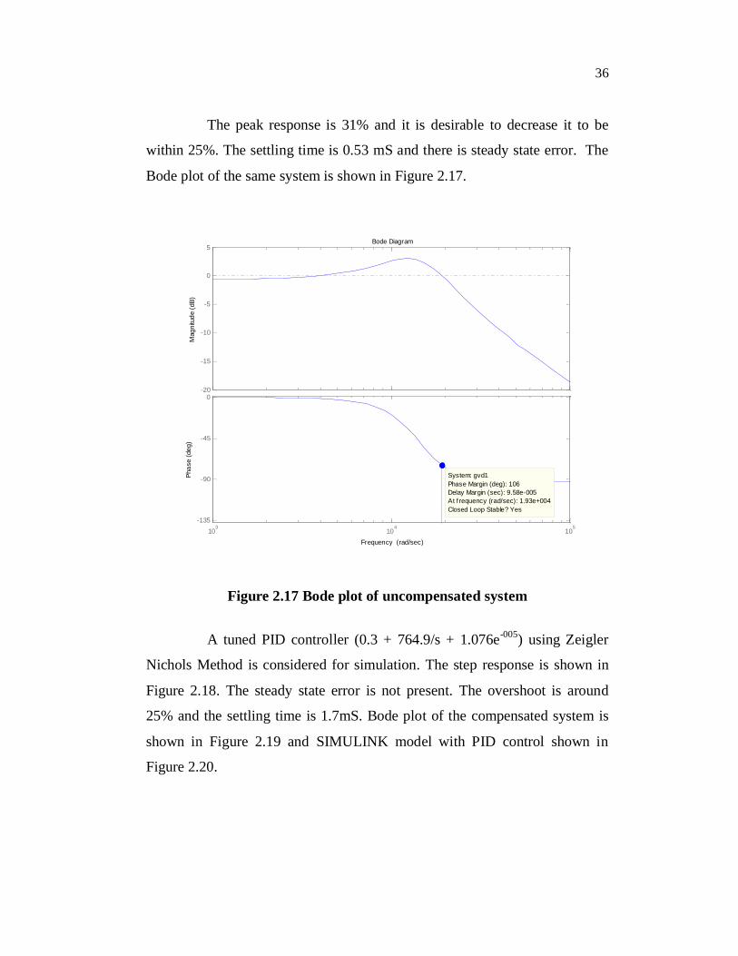
The peak response is 31% and it is desirable to decrease it to be
within 25%. The settling time is 0.53 mS and there is steady state error. The
Bode plot of the same system is shown in Figure 2.17.
Figure 2.17 Bode plot of uncompensated system
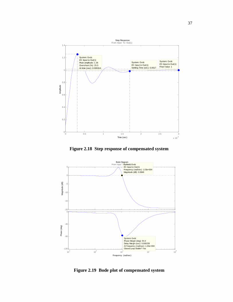
A tuned PID controller (0.3 + 764.9/s + 1.076e-005) using Zeigler
Nichols Method is considered for simulation. The step response is shown in
Figure 2.18. The steady state error is not present. The overshoot is around
25% and the settling time is 1.7mS. Bode plot of the compensated system is
shown in Figure 2.19 and SIMULINK model with PID control shown in
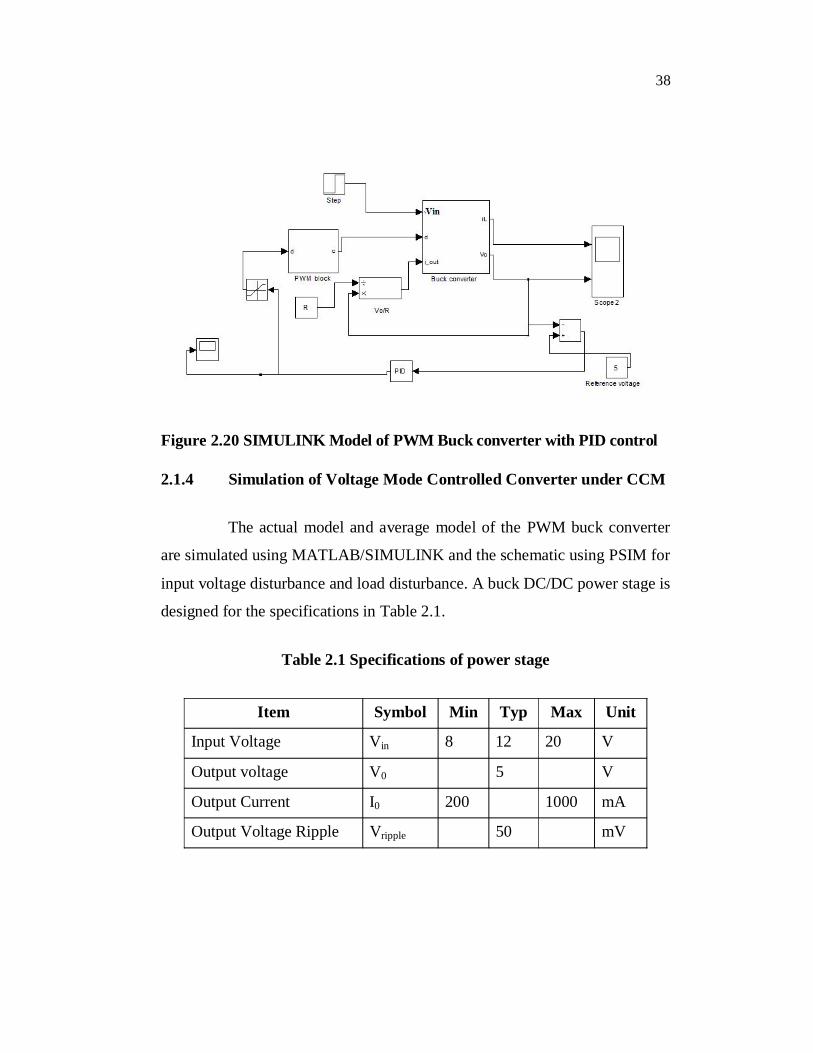
Figure 2.20.
-20
-15
-10
-5
0
5
Mag
nitu
de(d
B)
Bode Diagram
Frequency (rad/sec)10
310
410
5-135
-90
-45
0
System: gvd1Phase Margin (deg): 106Delay Margin (sec): 9.58e-005At f requency (rad/sec): 1.93e+004Closed Loop Stable? Yes
Phas
e(d
eg)
37
Figure 2.18 Step response of compensated system
Figure 2.19 Bode plot of compensated system
Step Response
Time (sec)
Ampl
itude
0 0.5 1 1.5 2 2.5 3
x 10-3
0
0.2
0.4
0.6
0.8
1
1.2
1.4
System: GvdcI/O: Input to Out(1)Final Value: 1
System: GvdcI/O: Input to Out(1)Settling Time (sec): 0.0017
System: GvdcI/O: Input to Out(1)Peak amplitude: 1.26Overshoot (%): 25.5At time (sec): 0.000314
From: Input To: Out(1)
-20
-15
-10
-5
0
5System: GvdcI/O: Input to Out(1)Frequency (rad/sec): 1.03e+004Magnitude (dB): 0.0848
From: Input To: Out(1)
Mag
nitu
de(d
B)
Bode Diagram
Frequency (rad/sec)10
210
310
410
510
6-135
-90
-45
0
System: GvdcPhase Margin (deg): 94.4Delay Margin (sec): 0.000159At f requency (rad/sec): 1.04e+004Closed Loop Stable? Yes
Phas
e(d
eg)
38
Figure 2.20 SIMULINK Model of PWM Buck converter with PID control
2.1.4 Simulation of Voltage Mode Controlled Converter under CCM
The actual model and average model of the PWM buck converter
are simulated using MATLAB/SIMULINK and the schematic using PSIM for
input voltage disturbance and load disturbance. A buck DC/DC power stage is
designed for the specifications in Table 2.1.
Table 2.1 Specifications of power stage
Item Symbol Min Typ Max Unit
Input Voltage Vin 8 12 20 V
Output voltage V0 5 V
Output Current I0 200 1000 mA
Output Voltage Ripple Vripple 50 mV

39
The following parameters in Table 2.2 are considered in the
simulation of the voltage mode controlled buck converter. Load resistance is
typically 5 Ohms corresponding to a load current of 1A and the load is varied
down to 100mA at light load.
Table 2.2 Parameter values considered for simulation
L 156uH
C 470uF
R 5 to 50 Ohms, 5 Ohms Typ
Vref 5V
T 25uS
vd 0.4
rC 0.125Ohms
2.1.4.1 Results
1. Input voltage at 12V, ref. voltage at 5V and the load current 1A
The output voltage is controlled to be constant at 5V when a
voltage of 12 V is applied as input. Load resistance R is chosen to be 5 . The
load current is 1A. The inductor current and output voltage of the converter
are shown in Figure 2.21.
The output voltage vo,max= 5.02 V and vo,min = 4.97V and the ripple
is 50mV p-p (approx).The inductor current ripple is 0.4A (approx).
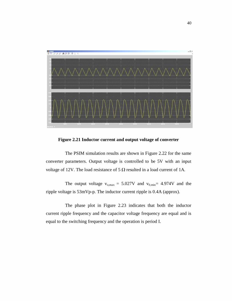
40
Figure 2.21 Inductor current and output voltage of converter
The PSIM simulation results are shown in Figure 2.22 for the same
converter parameters. Output voltage is controlled to be 5V with an input
voltage of 12V. The load resistance of 5 resulted in a load current of 1A.
The output voltage vo,max = 5.027V and v0,min= 4.974V and the
ripple voltage is 53mVp-p. The inductor current ripple is 0.4A (approx).
The phase plot in Figure 2.23 indicates that both the inductor
current ripple frequency and the capacitor voltage frequency are equal and is
equal to the switching frequency and the operation is period I.

41
Figure 2.22 Output voltage ripple for VM controlled buck converter
Figure 2.23 Phase plot between vC and iL showing period I operation
4.94
4.96
4.98
5
5.02
5.04 Output Voltage in V[0.204587 , 5.02721]
[0.204628 , 4.97428]
Ripple 1.058%
0.2046 0.2048 0.205Time (s)
0.7
0.8
0.9
1
1.1
1.2
1.3 Ind Current in A
0.70 0.80 0.90 1.00 1.10 1.20 1.30I2
4960.00m
4980.00m
5000.00m
5020.00m
5040.00m
vC in mV
42
0.0195 0.02 0.0205 0.021 0.0215 0.022
4.8
4.9
5
5.1
5.2
5.3
5.4
Time (S)
vo(v
)
PWM Converter Average Model - Response to Step Input Voltage Disturbance
0.0195 0.02 0.0205 0.021 0.0215 0.022
12
14
16
18
20
22
24
Time(S)
Vin
(V)
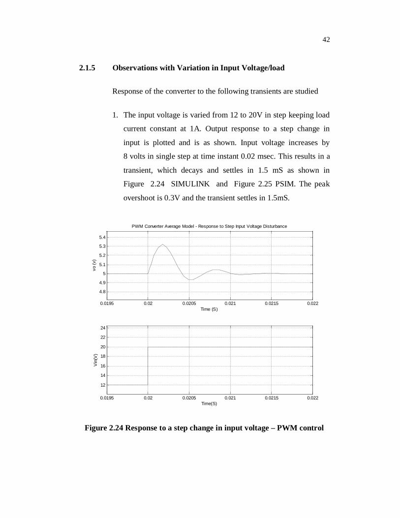
2.1.5 Observations with Variation in Input Voltage/load
Response of the converter to the following transients are studied
1. The input voltage is varied from 12 to 20V in step keeping load
current constant at 1A. Output response to a step change in
input is plotted and is as shown. Input voltage increases by
8 volts in single step at time instant 0.02 msec. This results in a
transient, which decays and settles in 1.5 mS as shown in
Figure 2.24 SIMULINK and Figure 2.25 PSIM. The peak
overshoot is 0.3V and the transient settles in 1.5mS.
Figure 2.24 Response to a step change in input voltage – PWM control

43
95.00 100.00 105.00Time (ms)
2.50
5.00
7.50
10.00
12.50
15.00
17.50
20.00
v 0(V
)v in
(V)
Figure 2.25 Response to a step change in input voltage – PWM control
The load is varied from 0.5A to 1 A at nominal input voltage of
12V.
Figure 2.26 Response to a step change in Load – PWM control
Time (S)
v o(V
)i o
(A)

44
Figure 2.27 Response to a step change in Load – PWM control simulated with PSIM
2.1.6 Bifurcation and Chaos in PWM DC DC Converter
Bifurcation is the qualitative change in the dynamics of a system
that occurs when a system parameter is changed (Di Bernado et al 1998, Dean
and Hamill 1990). It is a nonlinear phenomenon, which can be studied
through bifurcation diagrams, which is the most commonly used tool for
capturing bifurcation behavior.
The procedure for construction of the bifurcation diagram is as
follows:
1. Let µ be the parameter that is varied. Start with an initial value
of µ.
2. Generate a large number of say 1000 consecutive values of a
state variable x, from the iterative map of the form xn+1=f(xn).
3. Discard the initial transient, say, the rst 500 values. The
remaining 500 values of x form one data set.
96.00 98.00 100.00 102.00 104.00
0.0
1.00
2.00
3.00
4.00
5.00
6.00
Time (mS)
i o(A
)v o
(V)

45
4. With an increment in µ, repeat steps 2 and 3 for another data
set.
5. Repeat 4 over a chosen range of µ.
6. Plot each data set against µ.
The parameter, which is varied, is plotted along the x-axis and the
state variable is plotted along the y-axis. If the system were operating under
period I, for a particular parameter value, there would be one point along the
y-axis against that parameter value. If the system were operating at period II
at some other value of the parameter, then there would be two points against
that value. If the system were chaotic there would be a large number of points
against that value.
2.1.6.1 A Method to generate stepped input voltage variation
A method to obtain the bifurcation plot is described below. The
input voltage is taken as the parameter and is varied from a minimum voltage
to a maximum voltage up to which, the bifurcation plot is required. Every
level of the input voltage is maintained over a duration equal to that of 1000
cycles and data corresponding to the first 500 cycles in each level are not
considered to avoid data during transients that may be involved due to step
increase from one level to another.
Input voltage is increased in steps with the help of the following
circuit in Fig for bifurcation plot.

46
Figure 2.28 Schematic to generate a stepped input voltage variation
The up/down counter is set to count up and the square wave
oscillator frequency is selected suitably to include some 1000 cycles of clock
frequency. A voltage dependant voltage source accepts input from the counter
output and the source voltage increases in steps as the counter counts up.
Each voltage level stays constant over 1000 cycles of clock frequency. At the
end of 1000 cycles of clock the source voltage increases by 1 volt. It is
possible to alter the step size by adjusting the gain of the source. For example
if the gain is set to be 0.1 the voltage increases in steps of 0.1 and so on.
Figure 2.29 Stepped input voltage variation and sampling pulses
PEP0
U/DR
/C P
0.4 0.5 0.6T im e (s)
0
1 0
2 0
3 0
V5 V2

47
Figure 2.29 shows a typical source voltage waveform and the state
variable sampler pulses. Each burst of pulses represent 500 sampling pulses,
which sample the variable to be plotted. On every step increase in source
voltage, the sampling clock generates 1000 pulses but initial 500 pulses are
blanked out and are not present to avoid the transients due to step increase in
voltage. But in fact to determine the period doubling, sampling at two
successive clock cycles should be sufficient.
For the converter under study, for different input voltages the state
variable vC, is plotted against input voltage. Characteristic to be observed is
the periodicity of the operation and changes if any. Period I operation would
be observed when ripple frequency equals the switching frequency or the
frequency at which the system is driven. Stable converters exhibit periodic
steady state behavior. State variables repeat cyclically with period T.
Stroboscopic Poincar'e map, an important tool for studying stability of
periodic orbit replaces the continuous time system with an equivalent discrete
time system.
The Poincar'e map of equivalent discrete time system
nn RRxP :)( 0
0000 ,,)( xtTtxP with Ttt)( a periodic solution with
period I, has an attracting fixed point to which the state converges after
transients die down.
If the converter is not stable the fixed point is not an attractor and
there would be divergence away from the fixed point. Therefore stability of
the fixed point of the map determines the local stability and attracting fixed
point corresponds to periodic steady state of continuous time system. A fixed
48
point of a mapping is stable if and only if its characteristic multipliers or
Floquet multipliers all lie in the unit circle in the complex plane (Hamill D C
et al 1992). These multipliers are similar to gradient of the mapping in
one-dimensional case and are eigen values of the Jacobian evaluated at the
fixed point.
In the converter under study input voltage is varied from 12V to
20V for which it is designed. Stroboscopic map, plotted for iL, the inductor
current and vC, the capacitor voltage is observed using MATLAB/ SIMULINK.
The voltage is varied in small steps from 12V. In every step the
capacitor voltage, which is the state variable, during a particular instant in
each switching cycle is obtained. Due to this the map can be called as
stroboscopic switching map. Since there may be transient in each step voltage
for several initial cycles are discarded and after sufficient switching cycles
elapse the values are obtained and stored. During the same instants of time
inductor current is also obtained and stored.
These may be plotted with time instants to obtain the bifurcation
diagram. If the steps are close enough the diagram would be smooth. These
two state variables can be plotted with one as a function of other. The section
can be moved over the switching period wherein time is the third variable for
a particular input voltage. The strange attractor at a particular input voltage
and time instant within cycle is also obtained.
Period I operation is observed throughout and there was no
nonlinear phenomenon (Banerjee and Verghese 2001) exhibited over the
entire operating range which can also be studied using bifurcation diagram.
The fixed point on the phase plane, indicating period I operation for normal

49
input of 12V, is shown in Figure 2.30. State trajectory in state space
indicating period I operation is shown in Figure 2.31.
As the voltage is increased the operation changes to period II as
indicated by the phase plane plot in Figure 2.32 and the control voltage in
Figure 2.33.
Bifurcation diagram with input voltage as the parameter for the
PWM converter is shown in Figure 2.34.
In the converter under study, chaos, which is a bounded, aperiodic,
apparently random operation (Deane and Hamill 1990), sets in at a voltage of
about 23V. This is beyond the range at which the converter would normally
be operated and hence the converter is chaos free within normal range of
operation.
Figure 2.30 Phase portrait - Switching map – PWM converter
vC(V)
i L(A
)

50
Figure 2.31 State trajectory – PWM converter – period I operation
iL(A)
Figure 2.32 State trajectory in state space – PWM converter – period II operation
1.85 1.90 1.95 2.00 2.05 2.10 2.15
4980.00m
4990.00m
5000.00m
5010.00m
5020.00m
IL(A)
v C(V
)
0.60 0.80 1.00 1.20 1.40I2
4.875
4.90
4.925
4.95
4.975
5.00
5.025
5.05
VC
v C(V
)
51
Figure 2.33 Control voltage and ramp during period II operation
Figure 2.34 Bifurcation diagram for PWM converter input voltage in V is parameter
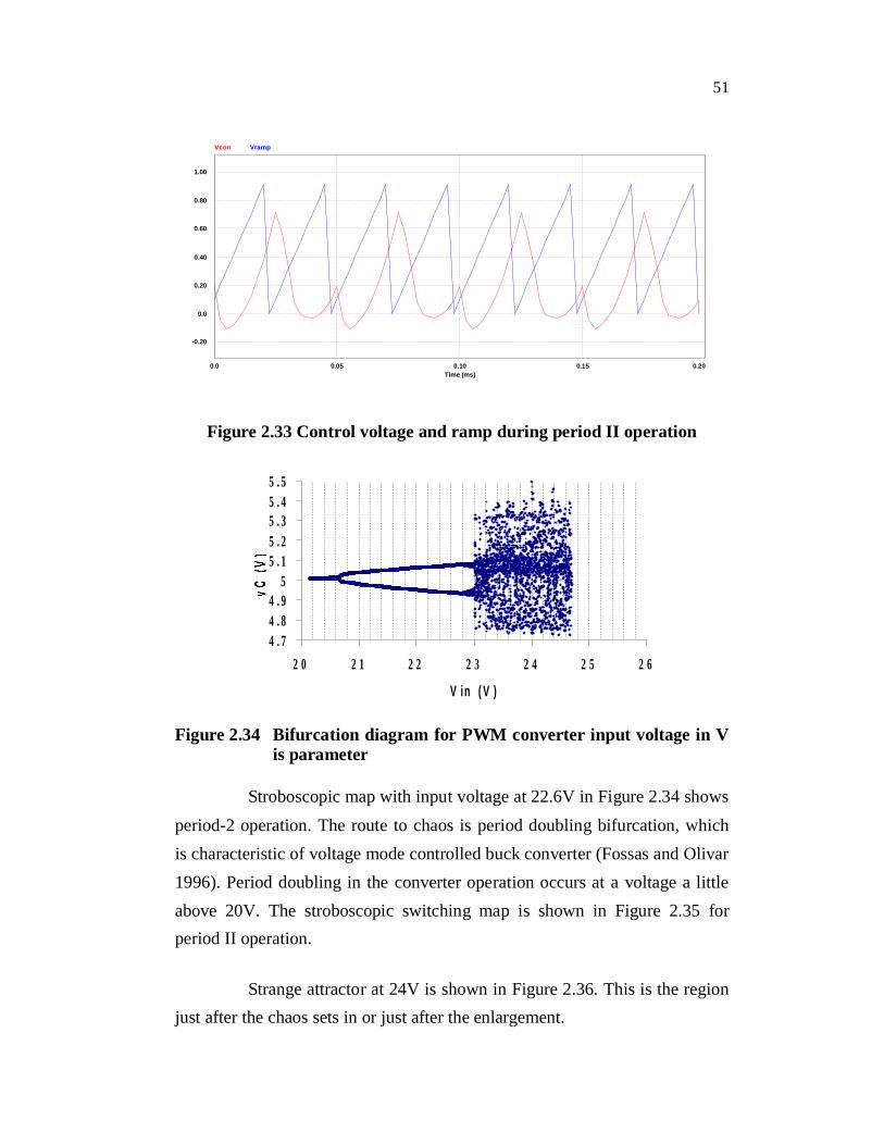
Stroboscopic map with input voltage at 22.6V in Figure 2.34 shows period-2 operation. The route to chaos is period doubling bifurcation, which is characteristic of voltage mode controlled buck converter (Fossas and Olivar 1996). Period doubling in the converter operation occurs at a voltage a little above 20V. The stroboscopic switching map is shown in Figure 2.35 for period II operation.
Strange attractor at 24V is shown in Figure 2.36. This is the region just after the chaos sets in or just after the enlargement.
0.0 0.05 0.10 0.15 0.20Time (ms)
0.0
-0.20
0.20
0.40
0.60
0.80
1.00
Vcon Vramp
4 . 74 . 84 . 9
55 . 15 . 25 . 35 . 45 . 5
2 0 2 1 2 2 2 3 2 4 2 5 2 6
V in ( V )
52
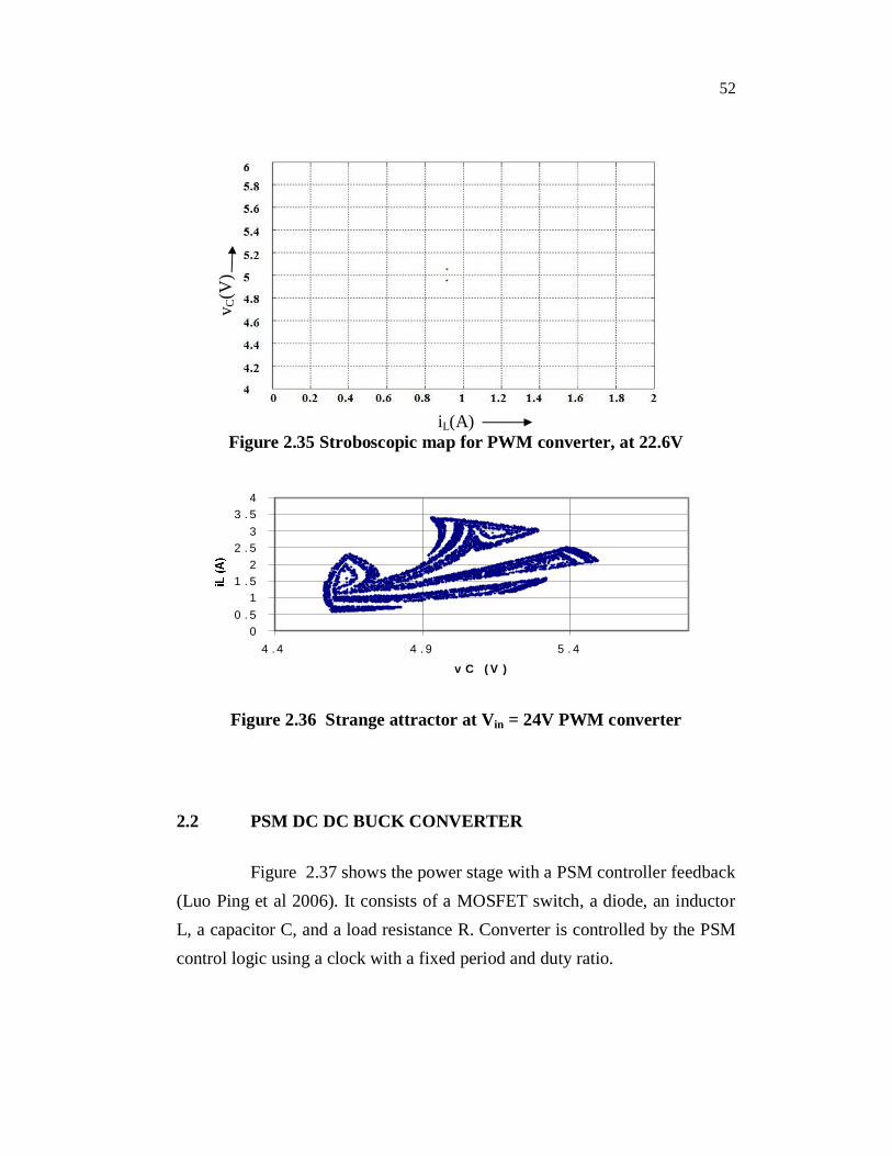
iL(A) Figure 2.35 Stroboscopic map for PWM converter, at 22.6V
Figure 2.36 Strange attractor at Vin = 24V PWM converter
2.2 PSM DC DC BUCK CONVERTER
Figure 2.37 shows the power stage with a PSM controller feedback (Luo Ping et al 2006). It consists of a MOSFET switch, a diode, an inductor L, a capacitor C, and a load resistance R. Converter is controlled by the PSM control logic using a clock with a fixed period and duty ratio.
00 . 5
11 . 5
22 . 5
33 . 5
4
4 . 4 4 . 9 5 . 4
v C ( V )
v C(V
)

53
Figure 2.37 PSM DC/DC buck converter
The clock pulses fed to the converter are at constant frequency and
the pulse width is set to be the maximum possible in a basic converter control.
The component values are selected for operation at clock frequency. The
frequency of operation is generally high enabling reduction in volume and
weight. Vin can be from a battery or rectified DC from mains that has double
the power frequency ripple.
2.2.1 Circuit Operation
While the converter output is less than the reference value, the
pulses are applied to the converter switch. When the converter output crosses
the reference, to go above the reference the next pulse is skipped. Hence
output is maintained at a value close to the reference. Pulse density decreases
after the output value goes above the reference or as load decreases and
increases when it goes below, or as the load decreases.
40kHz
V10/1V
+
-
Vref
L
C
+
-Vin
R
40kHz
V10/1V
+
-
Vref
L
C
+
-Vin
R
MOSFET
PSM CONTROL LOGIC
GATE/ INHIBIT
fSW
REF
SIG

54
MOSFET switch is ON when the clock pulse is applied over a xed
duration of time equal to duty cycle of the clock and the inductor current rises
linearly. The switch is OFF for the remaining period of the cycle and the
current drops to a lower value. It drops to a value lower than the initial value
if the next pulse is skipped and so on. Thus by alternately permitting p pulses
and skipping q pulses the output voltage is maintained at a value very close to
reference value. The waveforms are shown in Figure 2.38. The duration pDT
is known as charging duration and the duration qDT is known as skipping
duration. A cycle consists of (p+q) clock cycles each of duration T where T is
the switching period of the clock.
Figure 2.38 Waveforms of output voltage, inductor current and gate pulses for a PSM converter
D is the fixed duty ratio in each cycle and is the maximum duty
ratio possible and is less than 1.
0.2018 0.202 0.202 2 0.2024 0.2 026 0.2028 0.203 0.2032
0
2
4
6
8
10
Pulses Applied
Pulses skipped
vo
iL
Time (s)
vo(V
)&iL
(A)

55
Figure 2.39 PSM control logic
As shown in Figure 2.39(a) comparator compares v0 and vref and ts
output is given as D input to a D ip op. Q output of D ip op is ANDed
with CLK and the AND gate output s applied to the MOSFET switch. On
vref > v0 comparator output is HIGH and D is HIGH, which will also be the
output of the ip op as long as D is high throughout the clock cycle. This
makes the output of AND gate to equal the CLK and hence clock cycles are
applied to the switch. This duration is known as charging interval or active
interval. On vref < v0 comparator output is LOW and D ip op output goes
LOW at the rising edge of the CLK. This makes Q output of the ip op turn
LOW and hence the AND gate output is LOW irrespective of the CLK. The
clock pulses are not applied to the switch and are skipped. This duration is
known as skipping interval.
2.2.2 Operating Modes
2.2.2.1 Continuous conduction mode I
The converter is said to be working in continuous conduction mode
if the inductor current is greater than zero through out the cycle (Kapat et al
2008). In each cycle when the switch is ON the inductor current rises and
Q
Q
D
clk
Gate pulses
Vo
vref

56
when the switch is OFF the current drops to a value equal to or higher than
the initial value of the cycle at steady state. The current reaches a maximum
value at the end of the charging cycle. During the skipping cycle the pulses
are skipped and the current drops to a value higher than zero and the charging
cycle starts again. Typical waveforms of a converter working in continuous
conduction mode are shown in Figure 2.40.
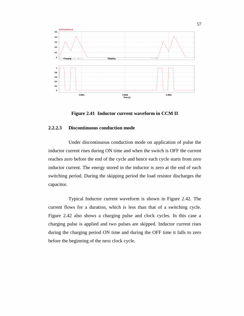
Figure 2.40 Inductor current waveform in CCM I
2.2.2.2 Continuous conduction mode II
Converter operates in continuous conduction mode with nonzero
inductor current except the initial value at the start of each charging cycle
(Angkititrakul and Hu 2008). In this mode the duration of skipping cycle is
long enough for inductor to dry out. The waveform shown in Figure 2.41 has
charging duration consisting of p cycles, skipping duration consisting of (q+r)
cycles where r is the number of cycles over which the inductor current is zero.
Here the inductor current is forced to become discontinuous by prolonging
the skipping period.
0
1
2
3
4
5
I2
Charging Skipping
0.4971 0.4972 0.4973 0.4974 0.4975Time (s)
0
0.2
0.4
0.6
0.8
1
V10
57
Figure 2.41 Inductor current waveform in CCM II
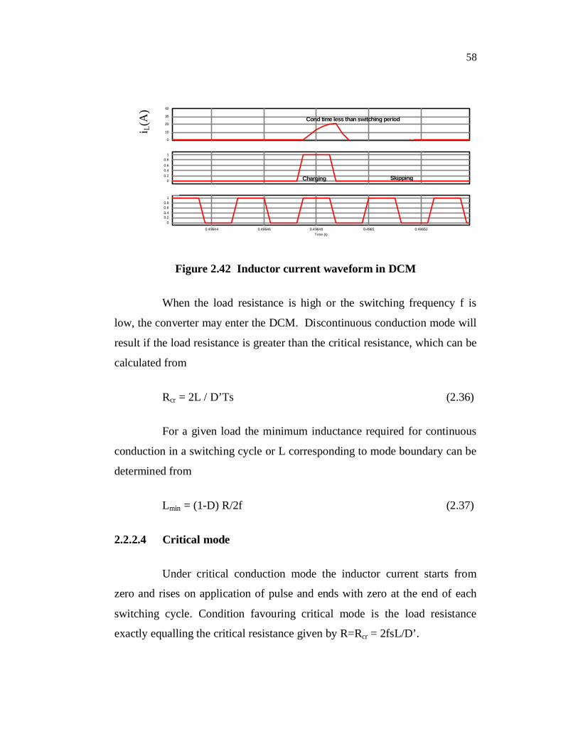
2.2.2.3 Discontinuous conduction mode
Under discontinuous conduction mode on application of pulse the
inductor current rises during ON time and when the switch is OFF the current
reaches zero before the end of the cycle and hence each cycle starts from zero
inductor current. The energy stored in the inductor is zero at the end of each
switching period. During the skipping period the load resistor discharges the
capacitor.
Typical Inductor current waveform is shown in Figure 2.42. The
current flows for a duration, which is less than that of a switching cycle.
Figure 2.42 also shows a charging pulse and clock cycles. In this case a
charging pulse is applied and two pulses are skipped. Inductor current rises
during the charging period ON time and during the OFF time it falls to zero
before the beginning of the next clock cycle.
0
0.1
0.2
0.3
0.4
0.5Ind Current in A
Charging Skipping
0.4951 0.4952 0.4953Time (s)
0
0.2
0.4
0.6
0.8
1
V10
58
Figure 2.42 Inductor current waveform in DCM
When the load resistance is high or the switching frequency f is
low, the converter may enter the DCM. Discontinuous conduction mode will
result if the load resistance is greater than the critical resistance, which can be
calculated from
Rcr = 2L / D’Ts (2.36)
For a given load the minimum inductance required for continuous
conduction in a switching cycle or L corresponding to mode boundary can be
determined from
Lmin = (1-D) R/2f (2.37)
2.2.2.4 Critical mode
Under critical conduction mode the inductor current starts from
zero and rises on application of pulse and ends with zero at the end of each
switching cycle. Condition favouring critical mode is the load resistance
exactly equalling the critical resistance given by R=Rcr = 2fsL/D’.
0
10
20
30
40I2
Cond time less than switching period
00.20.40.60.8
1
V10
Charging Skipping
0.49644 0.49646 0.49648 0.4965 0.49652Time (s)
00.20.40.60.8
1
V12
i L(A
)
59
Figure 2.43 Inductor current waveform in critical mode
Critical conduction mode is also known as Boundary Conduction
Mode or Border Conduction Mode. It is possible to derive the inductance for
a particular load that would result in critical conduction mode by taking the
inductor current ripple is twice the average value of the load current.
This inductance is known as critical inductance and for continuous
conduction for a particular load current the actual circuit inductance must be
greater than this. The conversion ratio calculated for continuous conduction is
valid only till this operation after which if the load current reduces or the
inductance reduces the conversion ratio drastically changes.
2.2.3 Modeling of Converter under Continuous Conduction Mode
Let charging period consists of p cycles and skipping period
consists of q cycles for a particular load resistance R and input voltage Vin.
The duration of charging period is pT and the duration of skipping period is
qT. During the charging period, in each cycle the switch is ON for duration
equal to DT where D < 1 and during the skipping period the switch is OFF
throughout T as the pulses are not applied and skipped. The converter is

60
modelled (Ping Luo et al 2006) using State Space Averaging (SSA) method
and the state space equations, assuming CCM, are obtained as shown below.
DTtforvBxAx in 011 (2.38)
xCy 1 (2.39)
TtDTforvBxAx in22 (2.40)
xCy 2 (2.41)
During skipping period
TtforvBxAx in 022 (2.42)
xCy 2 (2.43)
where
RCC
LAAA 11
1021 (2.44)
C
L
vi
x (2.45)
0vy (2.46)
0
11 LB (2.47)

61
02B (2.48)
10C (2.49)
Equations (2.38) to (2.41) are valid for p cycles and
Equations (2.42) and (2.43) are valid for q cycles. After State Space
Averaging,
inBDvqp
pAxx (2.50)
Defining Modulation Factor M,
ffM a1 (2.51)
where fa-Actual frequency of switch and f – Switching frequency
Then Equation (2.51) becomes
inDBvMAxx )1( (2.52)
Hence the average output voltage is given by
ino DvMv )1( (2.53)
Modulation factor M is proportional to the number of skipping. If
vin increases with v0 and D fixed, M increases. The number of pulses skipped
increases to maintain the voltage constant. A similar response is true for
increase in load. When load decreases M increases increasing the number of
skipping.

62
2.2.4 Simulation of PSM Buck Converter under CCM
The average model of the PSM buck converter is simulated using
MATLAB/SIMULINK and the schematic using PSIM. A buck DC/DC power
stage with the following parameters is considered. Parameter values for
power circuit are retained for comparison.
Table 2.3 Parameter values considered for simulation
S.No Parameter Value Unit
1 L 156 uH
2 C 470 uF
3R
5 to 50
5 Ohms Typical
Ohms
4 Vref 5 V
5 T 25 uS
6 vd 0.4 V
7 rC 0.125 Ohms
The actual topology model is simulated with SIMULINK – PSB as
in Figure 2.44 with parameters as in Table 2.1. A load resistance of 5 Ohm is
considered.
1. Input voltage is fixed at 12V; with reference voltage at 5V and
the load current is set to be 1A. The output voltage is controlled
to be constant at 5V when a voltage of 12 V is applied as input.
The output voltage and inductor current are as shown in
Figure 2.45.

63
powergui
Continuous
Voltage Measurement 1
v+-
Voltage Measurement
v+-
To Workspace
input 1
To File
psmtest .mat
Terminator
Series RLC Branch 2Series RLC Branch 1
Series RLC Branch
Scope 1
Scope
PulseGenerator
Mosfet
g m
D S
LogicalOperator
AND
Diode
DC Voltage Source
D Latch
D
C
Q
!Q
Current Measurement 1
i+ -
Current Measurement
i+ -
CompareTo Constant
< 5
Figure 2.44 PSM buck converter – SIMULINK – PSB
Figure 2.45 Inductor current for continuous conduction and output voltage. Ripple is observed to be slightly greater than 10%
v o(V
)i L
(I)

64
The PSIM simulation results are shown in Figure 2.46 below for the
same converter parameters.
Figure 2.46 PSIM Simulation output showing the ripple in v0 , Inductor current and pulses applied and skipped. Ripple is slightly above 10%
The state space averaged model is simulated with
MATLAB/SIMULINK and the response is shown below in Figure 2.47. Pulse
widths correspond to charging cycle consisting of a number of clock cycles
with constant pulse width with duty cycle of 80%. It is possible to note that
the width decreases as voltage increases and vice versa indicating the
regulating action.
Figure 2.47 Average model simulated with input voltage = 12V and D=0.8
4.4
4.8
5.2
5.6
6Output Voltag e v0 in V
00.5
11.5
2
Inductor Current in A
0.001 0.0015 0.002 0.0025 0.003 0.0035Time (s)
00.20.40.60.8
1
Pulses applied to S witch

65
2.2.5 Observations with Variation in Input Voltage/Load
For the converter under study the input voltage is changed in step
from 12V to 20V at 0.01 S. The output voltage settles in around 0.2mS with
higher ripple. The result indicates that the PSM converter has better response
to transients. Response to load current and input voltage is shown in
Figure 2.48.
(a)
(b)
Figure 2.48 Output voltage response to step change in (a) input and (b) load current
0
2
4
6
8
Output Voltage v0 in V
[0.0100016 , 5.59096]
[0.0102563 , 5.23008]
0.002 0.004 0.006 0.008 0.01 0.012 0.014Time (s)
12
14
16
18
20
step increase in Input Voltage
0
1
2
3
4
5
6V1
0.0096 0.0098 0.01 0.0102 0.0104 0.0106 0.0108 0.011 0.0112Time (s)
0.4
0.6
0.8
1
1.2
I1

66
2.2.6 Bifurcation and Chaos in PSM DC DC Converter
Input voltage is fixed at 12 V and the phase plane plot between iL,
the inductor current and vC, the capacitor voltage is plotted as shown in
Figure 2.49.
iL (A)
Figure 2.49 State trajectory in state space - plot between iL and vC with PSM control for Vin=12V
The poincar’e section as S-Switching map is drawn after the initial
transients subside completely and is shown in Figure 2.50. Period I operation
in which the ripple frequency equals the switching frequency is not observed
in this case, since the average frequency is less than the switching frequency
due to pulse skipping. Output voltage ripple is observed to be high,
demanding attention.
2.20 2.30 2.40 2.50 2.60 2.70 2.80I2
4.80
4.90
5.00
5.10
5.20
5.30
v C(V
)
67
Figure 2.50 Phase Portrait - Stroboscopic map – PSM converter for Vin=12V
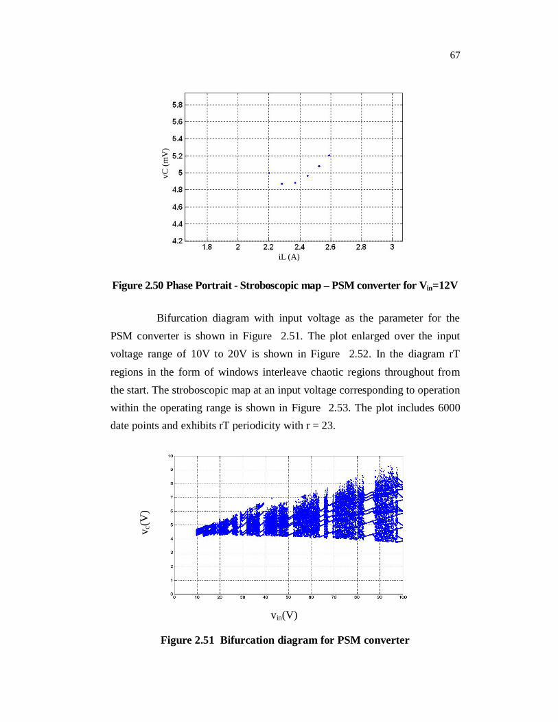
Bifurcation diagram with input voltage as the parameter for the PSM converter is shown in Figure 2.51. The plot enlarged over the input voltage range of 10V to 20V is shown in Figure 2.52. In the diagram rT regions in the form of windows interleave chaotic regions throughout from the start. The stroboscopic map at an input voltage corresponding to operation within the operating range is shown in Figure 2.53. The plot includes 6000 date points and exhibits rT periodicity with r = 23.
Figure 2.51 Bifurcation diagram for PSM converter
vC(m
V)
iL (A)
vin(V)
v c(V
)

68
Figure 2.52 Bifurcation diagram for PSM converter – enlarged over 10V to 20V range
Figure 2.53 Stroboscopic map for PSM converter at Vin = 17.6 V
For the same converter the voltage is changed in steps of 2V from 12V to 20 to observe the response for onset of chaos if any and the converter responded to be non chaotic as shown in Figure 2.54.
vin(V)
v c(V
)

69
Figure 2.54 Inductor current in A with change in input voltage in 2V steps from 12V to 20V
The Table 2.4 shows the pulses applied and skipped over the range
of input voltage.
Table 2.4 Pulses applied and skipped over the range of input voltage from 12V to 20V
Input Voltage Number of pulses Applied Skipped
12 10 2
14 6 2
16 4 2
18 3 2
20 2 2
0
0.5
1
1.5
2
2.5
3
106 4 3 2
0.202 0.203 0.204 0.205Time (s)
10
12
14
16
18
20

70
2.3 CONCLUSION
A DC to Dc converter is designed and controlled with PWM and PSM
controllers under continuous conduction node. The converters are model
studied for their performance under varying input voltage and load
conditions. It is found that PSM converter that better response, but suffers
from higher ripple. The converters are studied for exhibition of bifurcation
and chaos. A method to generate stepped input voltage variation is discussed
and the bifurcation diagrams and stroboscopic maps are obtained for both the
converters with supply voltage as parameter.