chapter 2 sol-gel preparation and characterization techniques...
TRANSCRIPT

20
CHAPTER – 2
SOL-GEL PREPARATION AND CHARACTERIZATION TECHNIQUES
2.1 Deposition techniques
The growth technique played a significant role in controlling the properties of ZnO
films, because the same material deposited by two different techniques, usually had different
physical properties. This is due to the fact that the electrical and optical properties of the
films strongly depended on the structure, morphology and nature of impurities present.
Moreover the films grown using any particular technique might have different properties due
to the variation of the deposition parameters and hence the properties can be tailored by
controlling the deposition parameters. Therefore, it is important and necessary to make a
detailed investigation on the different techniques used for the deposition of ZnO films. A lot
of methods have been extensively used for oriented ZnO films synthesis, including MBE,
pulsed laser deposition, sol-gel method, metal-organic chemical vapour deposition, sputtering
[37], cathodic magnetron sputtering, reactive electron beam evaporation [97–101], spray
pyrolysis [102-105] and electrodeposition [106, 107]. However, sol–gel processes are
particularly adapted to produce ZnO colloids [108–119] and films [120–126] due to the
following advantages such as,
Low cost.
Simple deposition equipment.
Easy fabrication of large-area films.
The idea behind sol-gel synthesis is to “dissolve” the compound in a liquid
and bring it back as a solid in a controlled manner.
Multi component compounds may be prepared with a controlled stoichiometry
by mixing sols of different compounds.

21
The sol-gel method prevents the problems encountered with co-precipitation
where inhomogeneity occurs during a gelation reaction.
Enables mixing at an atomic level.
Results in small particles, which can be easily sintered.
The sol–gel process, also called soft chemistry (‘chimie douce’), allows elaborating a solid
material from a solution by using a sol or gel as an intermediate step (Scheme 1) and at much
lower temperatures are possible by traditional methods of preparation. It enables the powder
less processing of glasses, ceramics and thin films or fibers directly from solution. The
synthesis of solid materials via ‘chimie douce’ often involves wet chemistry reactions while
sol–gel chemistry is based on the transformation of molecular precursors into an oxide
network by hydrolysis and condensation reactions [127, 128]. Scheme 1 shows the main
steps of preparation of thin films and powder by the sol-gel process.
The film preparation contains three parts: (i) preparation of the precursor solution,
(ii) deposition of the prepared sol on the substrate by the chosen technique and (iii) heat
treatment of the xerogel film. The xerogel is the dried gel at ambient pressure (dried gel in a
supercritical condition is called an aerogel). ZnO thin film synthesis involves several
parameters:
Nature of the precursor and its concentration,
Type of solvent and the acidity of the medium,
The type of additive species and their concentrations,
Aging time of the early mixture,
The method of coating of substrates and its speed,
Nature of the substrate,
Pre and post-heat treatment of the materials.

22
Scheme 1 Overview showing two synthesis examples by the sol–gel method; (a) films from a
colloidal sol; (b) powder from a colloidal sol transformed into a gel.
A survey of the literature shows that all these parameters play a key role in the evolution of
the texture in zinc oxide films.
2.2 Sol–gel method for zinc oxide synthesis
In the sol–gel process, a molecular precursor in a homogeneous solution undergoes a
succession of transformations: (a) hydrolysis of the molecular precursor; (b) polymerization
23
via successive bimolecular additions of ions, forming oxo-, hydroxyl or aquabridges; (c)
condensation by dehydration; (d) nucleation and (e) growth [129, 130]. Depending on the
nature of the molecular precursors, two sol–gel routes are currently used: metal alkoxides in
organic solvents or metal salts in aqueous solutions. The main methods of ZnO film
elaboration, as reported in the literature, involve several steps and are in fact intermediate
between the sol–gel methods since they use metal salts in alcoholic solutions. Indeed, ZnO
films are obtained starting from inorganic salts such as nitrates, chlorides, perchlorates or
organic salts like acetates and acetylacetonates, dissolved in alcoholic media. It is believed
that in such media the process involves two steps. The first one consists of in situ formation
of alkoxide or alkoxy-complexes. In the second step, these complexes undergo
transformation through hydrolysis and polymerization leading to the oxide formation.
2.2.1 Precursors
Several zinc precursors have been used in the preparation of ZnO. They are nitrate,
chloride, perchlorate, acetylacetonate and alkoxides such as ethoxide and propoxide, but the
most often used one is the acetate dihydrate. Metal alkoxides, although offer several chemical
advantages are not suitable because they are very sensitive to moisture, highly reactive and
expensive. Because of their low cost, facility of easy handling and commercial availability,
metal salts are interesting as precursors which could be more appropriate for large-scale
applications. Since metal salts include inorganic and organic ones, comparisons can be made
between them as reported by some authors [131]. Inorganic salts like nitrates are often used,
as precursors for sol–gel ZnO-based materials where the main drawback is related to the
inclusion of anionic species or their removal from the final product. Using zinc acetate as a
precursor, the acetate groups, as contaminants of the gel, decompose under annealing
producing combustion volatile by-products.
24
Bahnemann et al [110] synthesized transparent colloidal suspensions of zinc oxide in
water, 2-propanol and acetonitrile using different zinc salts. They reported that the anion, in
zinc salt is critical for the preparation of transparent and stable ZnO colloids. Also they
mentioned that the use of zinc perchlorate instead of zinc acetate yields a turbid suspension;
i.e coagulation of the particles takes place, the acetate act as a stabilizer of the colloidal sol.
The experiments with ZnCl2 or Zn(NO3)2 reveal a faster coagulation than in the case of
Zn(ClO4)2 following the initial formation of a clear colloidal suspension. Matijevic [108]
reported that the preparation of “monodispersed” sols of metal (hydrous) oxides from metal
salts is very sensitive to such factors as salt concentration, nature of the anion, pH and
temperature. He demonstrated that entirely different products result when the anions are
changed in the studied systems.
2.2.2 Solvents
The solvent must have a relatively high dielectric constant in order to dissolve the
inorganic salts [132, 133]. Most alcohols are dipolar, amphiprotic solvents with a dielectric
constant that depends on the chain length. Alcohols with low carbon number, up to 4 are the
most used solvents: methanol, ethanol, 1-propanol, 2-propanol, 1-butanol and
2-methoxyethanol. In addition, a few works use ethylene glycol (HOCH2CH2OH) as a
solvent that has a dielectric constant of 40.61 (at 25◦C) and a boiling point of 197.4◦C [134].
Among all the monoalcohols, the most used ones are ethanol and 2-propanol. It should be
noted that 2-methoxyethanol, despite having good physical properties, is toxic to
reproduction, because it is labelled with Risk Phrase R60 (category 2: ‘May impair fertility’)
by the International Programme on Chemical Safety, among others. Hosono et al. [133],
made a comparative study of chemical reactions from zinc acetate dihydrate to ZnO using
different types of alcoholic solvents, i.e. methanol, ethanol, and 2-methoxyethanol.

25
Zinc acetate dihydrate (ZAD) was more soluble in methanol than in ethanol or
2-methoxyethanol according to dielectric constants of these alcohols. The reflux time
necessary for the formation of ZnO increases with the solutions in the order, MeOH (12 h)
EtOH (48 h) < 2-ME (72 h). Besides, the same authors demonstrated that the XRD analysis
of particles, obtained from the three alcoholic solutions of ZAD revealed, after refluxing, the
formation of intermediate product as Zn5(OH)8(Ac)2·2H2O called layered hydroxide zinc
acetate (LHZA). This complex (LHZA) was also observed by Meulenkamp [117] using
ethanol as a solvent and by Fujihara et al. [136] using methanol. On the other hand,
Tokumoto et al. [138] have shown by EXAFS and UV spectroscopy that zinc acetate
dissolved in ethanol forms zinc oxy-acetate, Zn4O(Ac)6. Whatever be their nature, those
complexes undergo hydrolysis and inorganic polymerization leading to the formation of sols
consisting of zinc oxide nanoparticles. On the other hand, Hosono et al. [133] also showed
the washing role and the effect of the reflux time on the crystallinity and the size of particles.
It was found that LHZA was removed from the mixture particles, obtained with different
reflux times (from 8 to 48 h) in methanolic solution, by washing with MeOH. Both the XRD
peak intensities and the crystallite size are determined by using the Scherrer’s equation. They
increase monotonically with increasing reflux time, indicating the growth of the ZnO
particles where the crystallinity improves with time.
2.2.3 Additives
Additives are chemical species which present at least one functional group that
enables these species to play several roles. They act as basic or acid and/or chelating agents.
Alkali metal hydroxides, carboxylic acids, alkanolamines, alkylamines, acetylacetone and
polyalcohols are used for this purpose. They may facilitate the zinc salt dissolution in some
alcoholic media. For example, ZAD has a limited solubility in alcohols like ethanol and
2-propanol in the absence of other agents or heating.

26
The agents like (mono to tri) ethanolamines or lactic acid help in complete dissolution
and formation of a stable sol [135]. Furthermore, the additives are believed to play the role of
chelating and stabilizing ligands, which avoid the rapid precipitation of zinc hydroxide and
allow stable dispersions or solutions to be formed. The amino groups and/or the hydroxyl
groups of alkanolamines are known to coordinate the metal atoms of alkoxides, improving
the solubility and stability against hydrolysis of the alkoxides. This is also the case with zinc
acetate and the addition of alkanolamine provides a clear solution. There are two possible
ways for monoethanolamine (MEA) a bidentate ligand to coordinate the zinc atoms; one is to
act as a chelating ligand and the other is to bridge two zinc atoms [136]. Among inorganic
bases, lithium or sodium hydroxide is often used to form stable dispersions of colloids.
Altogether, solvents and additives are likely to react with zinc cations to give zinc complexes
that appear to be the precursor for zinc oxide. Several works have been devoted to the
structural characterization of such complexes. It has been proposed in previous works [137,
138], a mechanism for the reaction with the main species constituting the precursor solutions
(ZAD, ethanol and MEA) where additives such as MEA are employed. In this medium,
forced hydrolysis ([H2O]/[Zn2+] = 2) and condensation of the Zn2+ cation are relatively slow
due to the low quantities of water (resulting from zinc salt). MEA acts as a complexing agent,
also retarding Zn2+ condensation; however, the presence of this amine also increases the pH,
which should promote the formation of ZnO. The acetate group plays a very relevant role by
complexing Zn2+ in competition with the MEA. The complex chemical relationships of the
main species are indicated in Scheme 2. In fact, three nucleophilic species (MEA, OH− and
CH3COO−) compete for the Zn2+ Lewis acid center: attack of an HO− group leads to the
formation of small zinc-oxo-acetate oligomers, which are expected to be formed in the initial
stage, from gradual forced hydrolysis of Zn-MEA or Zn-OCOCH3 soluble complexes during
aging.
27
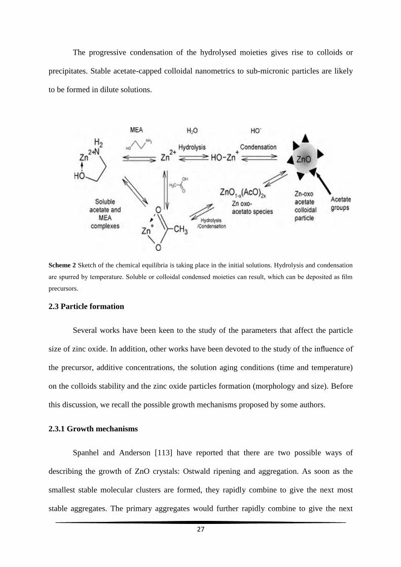
The progressive condensation of the hydrolysed moieties gives rise to colloids or
precipitates. Stable acetate-capped colloidal nanometrics to sub-micronic particles are likely
to be formed in dilute solutions.
Scheme 2 Sketch of the chemical equilibria is taking place in the initial solutions. Hydrolysis and condensation
are spurred by temperature. Soluble or colloidal condensed moieties can result, which can be deposited as film
precursors.
2.3 Particle formation
Several works have been keen to the study of the parameters that affect the particle
size of zinc oxide. In addition, other works have been devoted to the study of the influence of
the precursor, additive concentrations, the solution aging conditions (time and temperature)
on the colloids stability and the zinc oxide particles formation (morphology and size). Before
this discussion, we recall the possible growth mechanisms proposed by some authors.
2.3.1 Growth mechanisms
Spanhel and Anderson [113] have reported that there are two possible ways of
describing the growth of ZnO crystals: Ostwald ripening and aggregation. As soon as the
smallest stable molecular clusters are formed, they rapidly combine to give the next most
stable aggregates. The primary aggregates would further rapidly combine to give the next

28
most stable secondary aggregates and so on. The authors observed that the primary clusters
were stable aggregates and they could be a result of rapid aggregation rather than that of
Ostwald growth. Hence they concluded that the Ostwald mechanism should be considered as
the only one possible approach to the formation of bulk materials. Meulenkamp [117] also
suggested that the particle growth in colloidal systems could be viewed from two standpoints.
The first one corresponds to Ostwald ripening: large particles grow at the expense of smaller
particles, which have a higher solubility according to the Ostwald–Freundlich equation. This
relation is derived from thermodynamic equilibrium considerations and does not, therefore,
provide information on the growth rate. The second standpoint describes growth by the
addition of reactive precursors available in solution to already existing particles. The rate of
particle growth is governed by the concentration of precursors or dissolved species and their
reactivity, which depends on the number of particle surface atoms and the solution
composition. Tokumoto et al. [138] have reported that the formation of ZnO colloidal
particles in an alcoholic solvent consists of two stages. During the early stage of phase
transformation, small oligomers are continuously formed. At advanced stages, the
aggregation of the oligomers leads to wurtzite structure of the primary colloidal particles. The
primary particles then aggregate and form a third family of the secondary colloidal particles.
The growth of the colloidal particles is a stepped and discontinuous process indicating that
the predominant mechanism of aggregation is a heterogeneous coagulation. This mechanism
of formation and growth leads to a hierarchical structure.
2.3.2 Nucleation and growth – particle size
Spanhel [113] has reported that at least four different “primary particles or clusters”
serving as initiators of the ZnO colloidal growth from ZAD as precursor, could be identified
till date. The nature of these “primary particles or clusters” strongly depends on the synthesis
conditions chosen: initial salt concentration, the temperature, time of the thermal treatment,

29
the nature of alcohol solvent as well as the overall humidity, storage and analysis conditions.
Meulenkamp [117] has prepared ZnO nanoparticles by addition of LiOH to an ethanolic zinc
acetate solution. He showed that control of the particle size was improved by recognizing the
influence of temperature, water and reaction products during the aging of ZnO sols. Water
and acetate induced considerably accelerated particle growth. Hu et al. [119] have
synthesized ZnO nanoparticles by precipitation from zinc acetate in a series of n-alkanols
from ethanol to 1-hexanol as a function of temperature. The kinetics of nucleation and growth
are expected to be strongly dependent on the properties of the solvent. For the shorter chain
length alcohols, ethanol and 1-propanol, nucleation and growth are retarded compared to
longer chain length alcohols from 1- butanol to 1-hexanol, where nucleation and growth are
fast. The particle size increases with increasing temperature for all solvents and increases also
with alkanol chain length. In fact, during the growth of colloidal ZnO nanoparticles, the
alcohols not only provide the medium for the reactions, but also act as ligands to help control
the morphology and particle size of ZnO.
2.3.3 Morphology
Chittoffrati and Matijevic [112] have clearly showed that the precursor concentration
and the aging conditions as well as the nature and the concentration of the additive have an
important effect on the morphology of zinc oxide particles. Zinc oxide dispersions were
obtained by mixing at room temperature zinc nitrate or sulphate with different bases NaOH or
KOH, NH4OH, triethanolamine or ethylenediamine and cationic or anionic surfactants with
varied concentrations. It is followed by aging for different periods of time at constant
elevated temperatures. The authors have demonstrated that the precipitates formed by aging
zinc nitrate solutions at elevated temperatures, always consisted of zincite in ZnO, but the
shape and the size of the particles were strongly dependent on the concentration and nature of
the reactants. As a rule, particles uniform in shape and in some cases in size was obtained

30
only under a certain range of concentrations of the reacting compounds. For example, for the
system Zn(NO3)2–NH4OH turbidity appeared at room temperature, just after mixing, it with
[Zn(NO3)2] ≥ 3.2 × 10⁻⁴ mol L−1 and [NH4OH] ≥ 1.0 × 10⁻³ mol L−1. At much lower
concentrations of zinc nitrate and ammonia, no precipitation could be detected on mixing the
solution at room temperature. On the other hand by heating the diluted solution to 90◦C,
reasonably uniform ellipsoidal particles were obtained in small amounts. The particle shape
depends also on the concentrations and aging time since intertwined particles were obtained
with aging a solution of [Zn(NO3)2] = 5.0 × 10⁻³ mol L−1 and [NH4OH] = 1.9 × 10⁻² mol L−1
at 90◦C for 3 h, when ellipsoidal particles appeared with [Zn(NO3)2] = 1.0 × 10⁻⁴ mol L−1 and
[NH4OH] = 3.2 × 10⁻⁴ mol L−1 aged at 90◦C for 1 h. The particle shapes were changed by
Zn(NO3)2 in different solvents. For example, intertwined particles for Zn(NO3)2–
ethylenediamine, compact spheroidal or ellipsoidal particles for Zn(NO3)2–triethanolamine
and rod-like particles for Zn(NO3)2–KOH. Substituting ZnSO4 for Zn(NO3)2 yielded
polydispersed platelets in the case of Zn(NO3)2–triethanolamine system. The concentration
domain yielding uniform dispersions depend on the nature of the base employed. Indeed it
appeared that the stronger the Zn base complex, the lower the concentrations required to
generate well defined particles.
2.3.4 Colloids stability and thermal behaviour
The procedure for ZnO colloids synthesis, first developed by Spanhel and Anderson
[113], consists of two major steps: (1) preparing the precursor by reacting zinc acetate with
ethanol and (2) hydrolyzing the precursor to form the colloids by using lithium hydroxide.
Sakohara et al. [115], using this method, studied the concentration effect of zinc acetate
(ZnAc) and lithium hydroxide on the colloids stability as well as their behaviours during the
thermal analysis. The stability of ZnO colloids was observed to depend on the concentration
ratio, ZnAc/LiOH. The prepared colloids with a high ratio (e.g. ZnAc/LiOH = 0.1/0.025 M)

31
were quite stable and maintained transparency for more than a month, while a low ratio (e.g.
ZnAc/LiOH = 0.025 M/0.025 M) leads to a precipitate within 2 days. For thermal analysis of
ZnO particles, a weight loss was observed from about 200◦C with high ratios (e.g.
ZnAc/LiOH = 0.1 M/0.0125 M) but only from 300◦C for low ratios (e.g., ZnAc/LiOH =
0.0125 M/0.025 M). The acetate groups act so to stabilize colloids and this result was also
found by Bahnemann et al. [110] and Yang et al. [142]. Sun et al. [134] studied purification
and stabilization of colloidal ZnO nanoparticles synthesized from ZAD and potassium
hydroxide in methanol. They compared the stability of the purified ZnO nanoparticles
redispersed in methanol and in methanol/hexane solutions at two different volume ratios (7/1
and 3/1). The redispersed purified ZnO nanoparticles were unstable in methanol alone
because they become aggregated within several minutes at room temperature. In the case of
redispersion of ZnO nanoparticles in the mixture of methanol/hexane solutions, ZnO
nanoparticles would begin to agglomerate at room temperature after a couple of hours and 1
day for the mixtures with a volume ratio 7/1 and 3/1, respectively. So, hexane can stabilize
the purified ZnO nanoparticles in methanol and it has also demonstrated that the higher
concentration of hexane in the solution is more stable. The same authors have reported that a
possible reason why hexane can stabilize the purified ZnO nanoparticles in methanol could be
that a small amount of organic non-solvent, i.e. hexane, dissolved in methanol helps to reduce
the polarity of the solvent around the acetate-containing ZnO nanoparticle surfaces, thus
isolating the ZnO nanoparticles from each other and preventing them from aggregating.
2.4 Formation of oriented film
In general, films are prepared by dip or spin coating of substrate from solutions or sols
as freshly prepared or aged at 60◦C or around room temperature. The heat treatment of the
deposited films is carried out in two steps. In the first step, a pre-heat treatment (40–500◦C) is
applied for a short time for solvent evaporation and organic compounds removal [139–142].
32
In the second, a post-heat treatment is employed in order to obtain a well-crystallized films
and the final decomposition of organic by-products varying from 250 to 900◦C, according to
the substrate nature among others. The following examples of ZnO thin film elaboration are
given for illustration [143]. In these works, two approaches were explored to produce dense
films or colloid-based films. In the direct dense film formation ZAD was dissolved in a
2-methoxyethanol-MEA solution. The ratio ([MEA]/[Zn(II)]) was fixed at 1 or 2 and the final
concentration of ZAD was fixed at 0.75 mol L−1. The resultant mixture was allowed to stand
at 60◦C for 120 min under stirring leading to a clear and colourless solution, which remained
stable for several days. Freshly prepared solution was then deposited on silica glass by spin
coating at 3000 rpm (30 s). These films were pre-heated at 300◦C for 10 min after each
coating and this procedure was repeated up to six times. The films were post-heated at 550◦C
(1–2 h) in order to obtain crystallized ZnO in wurtzite structure. For the colloid-based films,
0.2 mol L−1 solution of Zn(II) was prepared by refluxing ZAD for 3 h at 80◦C in dry ethanol.
MEA and ethanol were subsequently added to adjust the final concentration (0.05 mol L−1 of
Zn2+) and the solutions were then aged at different temperatures (25–100◦C, in closed vessels)
during variable periods (10–240 h). Depending on the [Zn2+] and the ratio ([MEA]/[Zn2+]),
transparent solutions or colored colloidal dispersions (bluish to yellow) are obtained. The
solution aged at 60◦C for 72 h leads to a translucent yellow colored sol (colloidal dispersion).
The precursor sol was then filtered (Millipore cellulose membranes, 0.45 m) and
deposited on glass substrates by spin-coating 3000 rpm for 30 s. These films were dried at
100◦C for 5 min between successive spin-coating steps. Subsequently, they were pre-treated
at 135◦C for 36–72 h and further post-treated at 450–550◦C for 2 h.

33
2.4.1 Role of the heat treatments: pre-heat treatment and post-heat treatment
The heat treatment appears to be one of the most important factors governing the film
orientation. As discussed above, the pre-heat treatment appears to be a crucial step. Indeed, it
governs the orientation of the crystallites during solvent evaporation and removal of the
organic compounds. The temperature of this treatment varies from case to case, but a clear
rule can be deduced from a proper choice. It should be higher than the boiling point of the
solvent, the additives and near the crystallization temperature of ZnO. A temperature around
300◦C appears to be the most appropriate [144, 145] in the case of 2-methoxyethanol and
MEA as solvent and additive, respectively, to produce (002) oriented films. This temperature
has also been observed for the system consisting of methanol and lactic acid. On the contrary,
a pre-heat temperature of 100◦C for the films obtained from 2-propanol and DEA was
sufficient for observing full (002) orientation. A similar low pre-heat temperature (80◦C) has
also been used for the chemical systems consisting of methanol as solvent without using any
additives [146]. Beside the pre-heat and post-heat temperature should be carefully chosen.
The preferential orientation, for instance (002), increases with increasing temperature. For, a
great number of systems, a temperature range of 500–600◦C appears to be the most
appropriate one. However, it should be noted that there exists for each system an upper limit
in temperature above which the loss of orientation is observed. The pre-heat temperature
seems to be the most important factor for obtaining ZnO films with preferred orientation
[147], affecting the solvent vaporization, zinc acetate decomposition and zinc oxide crystal
growth. Removal of the solvent and organic substances produced by acetate decomposition
prior to crystallization may be one of the key factors that provide oriented crystal growth
[148, 149].

34
2.5 Spin Coating Method
Spin coating is currently the predominant technique employed to produce uniform
thin films of photosensitive organic materials with thickness of the order of micrometers and
nanometers. The pioneering analysis of spin coating was performed more than fifty years ago
by Emisle et al [151] who considered the spreading of a thin axisymmetric film of Newtonian
fluid on a planner substrate rotating with constant angular velocity. In many cases the coating
material is polymeric and is applied in the form of a solution from which the solvent
evaporates. Spin coating was first studied for coating of paint and pitch [150]. This process
has been widely used in the manufacture of integrated circuits [151], optical mirrors, color
television screens and magnetic disk for data storage [152]. Centrifugal force drives the liquid
radially outward. The viscous force and surface tension causes a thin residual film to be
retained on the flat substrate. The thin nature of the film depends on the combination of
outward fluid flow and evaporation [153]. The spin coating can be broken down into several
key stages: fluid dispense, spin-up, stable fluid out flow and finally evaporation dominated
drying [154]. Flow controlled and evaporation controlled are the two stages that have the
most impact on final coating thickness. Clearly it’s describe the two processes that must be
occurring simultaneously throughout all times (viscous flow and evaporation). However, at
an engineering level the viscous flow effect dominates early on, while the evaporation
processes dominate later. Fluid flow on a flat spinning substrate is one of the most important
physical processes involved in spin coating [155]. Several processing parameters involved in
the spinning process are: dispense volume, final spin speed (w), final film thickness, solution
viscosity, solution concentration (c), spin time, etc. Using different parameters film thickness
and radius of spreading are calculated [156]. The film forming process is primarily driven by
two independent parameters viscosity and spin speed. The range of the film thickness easily
achieved by spin coating is 1–200 µm [157, 158].

35
2.5.1 Modelling of spin coating
Even though spin coating has been universally used in the semiconductor industry
long before, hardly any theoretical study has been initiated. An accurate theory of spin
coating would permit better design and control of the process in its various applications.
Decades of industrial production have shown that the depositions of thin photoresists films,
which constitute the main utilization of the spin coating process are quasi-perfectly
controlled. However, any progress in developing mathematical models should be probably
more helpful in the case of heat resistant dielectric insulating films (polyamides or other
materials). In contrast to the photoresists which are often low molecular weight materials
dissolved in low boiling solvents at low concentration, polyimide precursors are high
molecular weight polymers. These materials are supplied in organic solvents with boiling
temperatures close to 200°C per concentration levels (10–20%), where the non-Newtonian
behaviors cannot be neglected. This implies that spin analytical models will be based on
sophisticated equation taking in consideration a number of physical parameters.
2.5.2 Key stages of spin coating
The physics of spin coating can be effectively modeled by dividing the whole process
into four stages is sketched in Fig.2.1. They are deposition, spin-up, spin-off and evaporation
of solvents. The first three are commonly sequential, but spin-off and evaporation usually
overlap.

36
Fig.2.1 Key stages of spin coating process.
37
Deposition
During this stage, solution is allowed to fall on rotating substrates from microsyrings
and the substrate is accelerated to the desired speed. Spreading of the solution takes place due
to centrifugal force and height is reduced to critical height. This is the stage of delivering an
excess of the liquid to be coated to the surface of the substrate a portion of which is
immediately covered or “wetted”. In this stage liquid can be deposited in different ways (a)
as a heavy rain that inundates the entire disk, (b) as a bolus at the centre or around the
perimeter of hole if the centre has been cut out, the liquid then spreading over the rest of the
disk, (c) as a continuous stream at the centre or all the way around the inner perimeter, the
liquid then flowing outward over the entire disk, (d) as a continuous stream from an elevated
delivery port that moves racially over the disk. No matter what way is used the amount of
liquid deposited through excessive is limited and this stage ends when delivery ceases.
Spin-up
The second stage is when the substrate is accelerated up to its final, desired, rotation
speed. This stage is usually characterized by aggressive fluid expulsion from the wafer
surface by the rotational motion. Because of the initial depth of fluid on the wafer surface,
spiral vortices may briefly be present during this stage; these would form as a result of the
twisting motion caused by the inertia that the top of the fluid layer exerts while the wafer
below rotates faster and faster. Eventually, the fluid is thin enough to be completely
co-rotating with the wafer and any evidence of fluid thickness differences is gone.
Ultimately, the wafer reaches its desired speed and the fluid is thin enough that the viscous
shear drag exactly balances the rotational accelerations
Stable fluid out flow
The third stage is when the substrate is spinning at a constant rate and fluid viscous
forces dominate fluid thinning behaviour. This stage is characterized by gradual fluid

38
thinning. Fluid thinning is generally quite uniform, though with solutions containing volatile
solvents; it is often possible to see interference colors “spinning off” and doing so
progressively more slowly as the coating thickness is reduced. Edge effects are often seen
because the fluid flows uniformly outward, but must form droplets at the edge to be flung off.
Thus, depending on the surface tension, viscosity, rotation rate, etc., there may be a small
bead of coating thickness difference around the rim of the final wafer. Mathematical
treatments of the flow behavior show that if the liquid exhibits Newtonian viscosity (linear)
and if the fluid thickness is initially uniform across the wafer (albeit rather thick), then the
fluid thickness profile at any following time will also be uniform.
Evaporation
When spin-off stage ends the film drying stage begins. During this stage centrifugal
out flow stops and further shrinkage is due to solvent loss. This results in the formation of
thin film on the substrate. The fourth stage is when the substrate is spinning at a constant rate
and solvent evaporation dominates the coating thinning behaviour. In this, the rate of
evaporation depends on two factors (a) the difference in partial pressure (actually chemical
potential) of each solvent species between the free surface of the liquid layer and the bulk of
the gas flowing nearby. (b) during the evaporation stage the suspended or dissolved solids
may grow so concentrated at the liquid surface as to form a high viscosity, low diffusivity
layer or solid skin.
2.6 Characterization tools
The optimisation of the preparation conditions is the main task in order to get
device quality films. This has to be carried out on the basis of detailed structural,
compositional, morphological, optical and electrical properties of the films obtained at
different growth conditions. In the following sections the techniques used for the film
characterizations are discussed briefly.

39
2.6.1 Thin film thickness
Thickness plays an important role in the film properties unlike a bulk material.
Reproducible properties are achieved only when the film thickness and the deposition
parameters are kept constant. Film thickness may be measured either by in-situ monitoring
of the rate of deposition or after the film deposition. The thicknesses of the thin films
prepared for the work presented in this thesis were measured either by optical interference
method or by a stylus profiler.
i) Optical interference method
Film thickness can be measured accurately from interference fringes using multiple
beam interferometry. This technique was first used by Weiner [161] and later was modified
by Tolansky [162]. Two reflecting surfaces are brought in close proximity such that a small
wedge with a small air gap in between them is formed. If a monochromatic light falls at
normal incidence on it, interference of light due to the multiple reflected beams results in a
series of fringes (Fizeau). The distance between the fringes depends on the air gap as well
as the wavelength of the monochromatic light. The film whose thickness is to be measured
is deposited on a flat surface so as to leave a sharp edge between the film and the uncoated
region of the substrate. Over this film a highly reflecting coating of aluminium forms a sharp
step on the film edge. Another optically flat glass slide known as the reference plate with a
partially transparent aluminium film coated over it is then placed over the specimen with the
metal coated surfaces in contact with each other so as to leave a small air gap at the step. A
monochromatic parallel beam of light (λ) is made to fa l l on the two plate’s assembly
and the reflected light is then observed through a microscope. A set of sharp fringes
perpendicular to the step with equal displacements will be observed.

40
The thickness (t) can be determined using the relation,
𝑡 = 𝑏𝜆
2𝑎 (1)
where ‘b’ is the displacement of the fringes at the step and ‘a’ is the distance between
consecutive fringes. The sharpness of the fringes depends on the reflectivity of the metal
coating, the spread of the incident beam, air gap etc.
ii) Stylus Profiler
The stylus profiler records measurements electromechanically by moving the sample
beneath a diamond tipped stylus (Fig. 2.2).
Fig. 2.2 Schematic diagram illustrating the determination of thin film
thickness with stylus profiler
The high precision stage moves the sample according to a user defined scan length,
speed and stylus force. The stylus is mechanically coupled to the core of a linear variable
differential transformer (LVDT). At this stage the stylus moves over the sample surface.
Surface variations cause the stylus to be translated vertically. Electrical signals corresponding
to the stylus movement are produced as the core position of the LVDT changes. The LVDT
measures an AC reference signal proportional to the position change, which in turn is
conditioned and converted to a digital format through a high precision, integrating, analog-to-
digital converter [159]. The film whose thickness has to be measured is deposited with a

41
region masked this creates a step on the sample surface the thickness of the sample can
be measured accurately by measuring the vertical motion of the stylus over the step.
2.6.2 X-ray diffraction studies
Electrical and optical properties of the thin films grown are influenced by the
crystallographic nature of the films. X-ray diffraction (XRD) studies are carried out to study
the crystallograoghic properties of the thin films prepared. A given substance always
produces a characteristic X-ray diffraction pattern irrespective of the fact that the substance
is present in the pure state or as one constituent of a mixture of substances. This fact is the
basis for the diffraction method of chemical analysis. The particular advantage of X-ray
diffraction analysis is that it discloses the presence of a substance which is not in terms of its
constituent chemical elements. Diffraction analysis is useful whenever it is necessary to
know the state of chemical combination of the elements involved or the particular phase in
which they are present. Compared with ordinary chemical analysis the diffraction method
has the advantage that it is much faster, requires only very small sample and is non-
destructive [160]. The basic law involved in the diffraction method of structural analysis is
the Bragg’s law. When monochromatic X-rays impinge upon the atoms in a crystal
lattice, each atom acts as a source of scattering. The crystal lattice acts as series of
parallel reflecting planes. The intensity of the reflected beam at certain angles will be
maximum when the path difference between two reflected waves from two different planes
is an integral multiple of ‘λ’. This condition is called Bragg’s law and is given by the
relation,
2𝑑𝑆𝑖𝑛𝜃 = 𝑛𝜆 (2)
where ‘n’ is the order of diffraction, ‘λ’ is the wavelength of the X-rays, ‘d’ is the spacing
between consecutive parallel planes and ‘θ’ is the glancing angle (or the complement of

42
the angle of incidence) [161]. X-ray diffraction studies gives a whole range of information
about the crystal structure, orientation, average crystalline size and stress in the films.
Experimentally obtained diffraction patterns of the sample are compared with the
standard powder diffraction files published by the International Centre for Diffraction Data
(ICDD). The average grain size of the film can be calculated using the Scherrer’s formula
[162],
𝑑 = 0.9𝜆
𝛽𝐶𝑜𝑠𝜃 (3)
where, ‘λ’ is the wavelength of the X-ray and ‘β’ is the full width at half maximum
intensity in radians. The lattice parameter values for different crystallographic systems can
be calculated from the following equations using the (hkl) parameters and the interplanar
spacing (d).
𝐶𝑢𝑏𝑖𝑐 𝑠𝑦𝑠𝑡𝑒𝑚, 1
𝑑2=
ℎ2 + 𝑘2 + 𝑙2
𝑎2
𝑇𝑒𝑡𝑟𝑎𝑔𝑜𝑛𝑎𝑙 𝑠𝑦𝑠𝑡𝑒𝑚, 1
𝑑2=
ℎ2 + 𝑘2
𝑎2+
𝑙2
𝑐2
𝐻𝑒𝑥𝑎𝑔𝑜𝑎𝑛𝑎𝑙 𝑠𝑦𝑠𝑡𝑒𝑚, 1
𝑑2=
4
3 (
ℎ2 + ℎ𝑘 + 𝑘2
𝑎2) +
𝑙2
𝑐2
X-ray diffraction measurements of the films in the present studies were done by copper Kα
(λ=1.5406 A ) radiation was used for recording the diffraction pattern.
2.6.3 Scanning electron microscope (SEM)
The scanning electron microscope is a microscope that uses electrons rather than
light to form an image. There are many advantages in using SEM instead of an optical
microscope [163]. The SEM has a large depth of field, which allows a large amount of the
sample to be in focus at one time. The SEM also produces images of high resolution, which
means that closely spaced features can be examined at a high magnification. Preparation of
43
the samples is relatively easy since most SEMs only require that the sample should be
conductive. The combination of higher magnification, larger depth of focus, greater
resolution and ease of sample observation make the SEM as one of the appropriate
instruments used in current research and development. The electron beam comes from a
filament, made of various types of materials. The most common is the tungsten hairpin gun.
This filament is a loop of tungsten that functions as the cathode. A voltage is applied to the
loop, causing it to heat up.
The anode, which is positive with respect to the filament, forms powerful attractive
forces for electrons. This causes electrons to accelerate toward the anode. The anode is
arranged, as an orifice through which electrons would pass down to the column where the
sample is held. Other examples of filaments are lanthanum hexaboride filaments and field
emission guns. The streams of electrons that are attracted through the anode are made to
pass through a condenser lens and are focused to very fine point on the sample by the
objective lens (Fig. 2.3). The electron beam hits the sample, producing secondary electrons
from the sample. These electrons are collected by a secondary detector or a backscatter
detector, converted to a voltage and amplified. The amplified voltage is applied to the grid
of the cathode ray tube (CRT) that causes the intensity of the spot of light to change. The
image consists of thousands of spots of varying intensity on the face of a CRT that
correspond to the topography of the sample.
Fig. 2.4 shows the interaction of electrons with matter in order to make sure that the
information comes from the sample surface only, when a SEM is used, the column must
always be at a vacuum. Otherwise there are chances for contamination of the sample and
also the electrons beam would induce ionisation in any background gas that would affect
the measurement being made on the sample.

44
Fig. 2.3 The focusing of electrons in SEM
Fig. 2.4 In SEM set up, interaction of electron with the sample produces both
photons and electrons.
2.6.4 Energy dispersive X-ray (EDX) spectra
EDX analysis stands for energy dispersive X-ray analysis. It is sometimes referred to
as EDAX analysis. It is a technique used for identifying the elemental composition of the
specimen, or an area of interest thereof. The EDX analysis system works as an integrated

45
feature of a scanning electron microscope (SEM) and cannot operate on its own without the
latter [164, 165]. During EDX analysis, the specimen is bombarded with an electron beam
inside the scanning electron microscope. The bombarding electrons collide with the
specimen atom’s own electrons, knocking some of them off in the process. A higher-energy
electron from an outer shell eventually occupies a position vacated by an ejected inner shell
electron. To be able to do so, however, the outer electron must give up some of its energy
by emitting X-ray. The amount of energy released by the transferring electron depends on
which shell it is transferring from, as well as which shell it is transferring to. Furthermore,
the atom of every element releases X-rays with unique amounts of energy during the
transferring process. Thus, by measuring the energy of the X-rays emitted by a specimen
during electron beam bombardment, the identity of the atom from which the X-ray was
emitted can be established. The EDX spectrum is a plot of intensity of X-ray Vs energy of
the emitted X-ray. An EDX spectrum normally displays peaks corresponding to the energy
levels for which the most X-rays have been received. Each of these peaks is unique to an
atom, and therefore corresponds to a single element. The higher intensity of a peak in the
spectrum is more concentrated element in the specimen. An EDX spectrum plot not only
identifies the element corresponding to each of its peaks, but the type of X-ray to which it
corresponds as well. For example, a peak corresponding to the amount of energy possessed
by X-rays emitted by an electron in the L-shell going down to the K-shell is identified
as Kα peak. The peak corresponding to X-rays emitted by M-shell electrons going to the
K-shell is identified as a Kβ peak as shown in Fig. 2.5.

46
Fig. 2.5. Electronic transitions are showing the emission of X- rays.
2.6.5 Atomic force microscopy (AFM)
Following the invention of the scanning tunnelling microscope (STM), a number of
new scanning probe microscopes (SPM) has been developed that use the key
components of the STM. One of the most important SPM is the atomic force microscope
(AFM) [166]. In atomic force microscopy a tip is integrated to the end of a spring
cantilever, is brought within the interatomic separations of a surface, such that the atoms of
the tip and the surface are influenced by interatomic potentials. As the tip is restored across
the surface, it bounces up and down with the contours of the surface. By measuring the
displacement of the tip (i.e. the deflection of the cantilever), one can theoretically map out
the surface topography with atomic resolution. The first generated AFM's measured
cantilever deflections using a piggy-backed STM. Later instruments are used for more
practical optical techniques. The AFM is essentially identical in concept to the scanning
profilometer, except that the deflection-sensitivity and resolution are improved by several orders
of magnitude. There are a large number of applications for the AFM, including biological
systems, polymers and a host of insulator and semiconductor materials.

47
Fig. 2.6 The essential elements of an AFM
An AFM images a surface in a manner analogous to the gramophone stylus sensing
the groves of gramophone disk. The essential elements of an AFM are shown in Fig.2.6.
The tip is attached to a cantilever type spring as shown in the Fig.2.7.
Fig. 2.7 Attachment of the tip to the cantilever in an AFM.

48
As the tip and sample interact, forces act on the tip and cause the cantilever (spring)
to deflect. The cantilever position is monitored by a position detector. The output of the
detector is connected to a feedback controller that regulates the force between the sample
and the tip by moving the sample up or down. The sample is moved by a PZT (lead
zirconate titanate) scanning actuator. The cantilever must be soft enough to deflect a
measurable amount without damaging the surface features of the sample. The amount of
deflection is proportional to the force acting on the tip.
𝐹𝑠𝑝𝑟𝑖𝑛𝑔 = −𝑘 . ∆𝑍 (4)
where ‘F’ is the force on the sample, ‘k’ is the spring constant of the cantilever and ‘∆Z’ is the
deflection of the cantilever. Various modes of AFM measurements are contact mode, dynamic
force mode and phase mode. Friction force microscope, magnetic force microscope, surface
potential microscope, etc., are all scanning probes microscopes with slight variation in the working
principles from that described above.
2.6.6 Raman spectroscopy
Raman spectroscopy is a commonly used vibrational, optical and mostly non-
invasive research method, for example used in chemical analysis and in solid state physics.
Amongst others, it has been successfully applied to investigate semiconductor systems, e.g.
in heterostructures and at interfaces. Raman spectroscopy is based upon the inelastic
scattering of monochromatic light within the studied sample, accompanied by the
generation or annihilation of elementary excitations. In this thesis mostly the elementary
excitations of vibrations and the particularly lattice vibrations (phonons) are dealt. Raman
spectroscopy then provides access to the lattice dynamics of a sample and thereby delivers
information on structural properties like chemical composition, orientation or crystalline
quality. In addition, electronic and magnetic properties can be addressed, e.g. by Raman
49
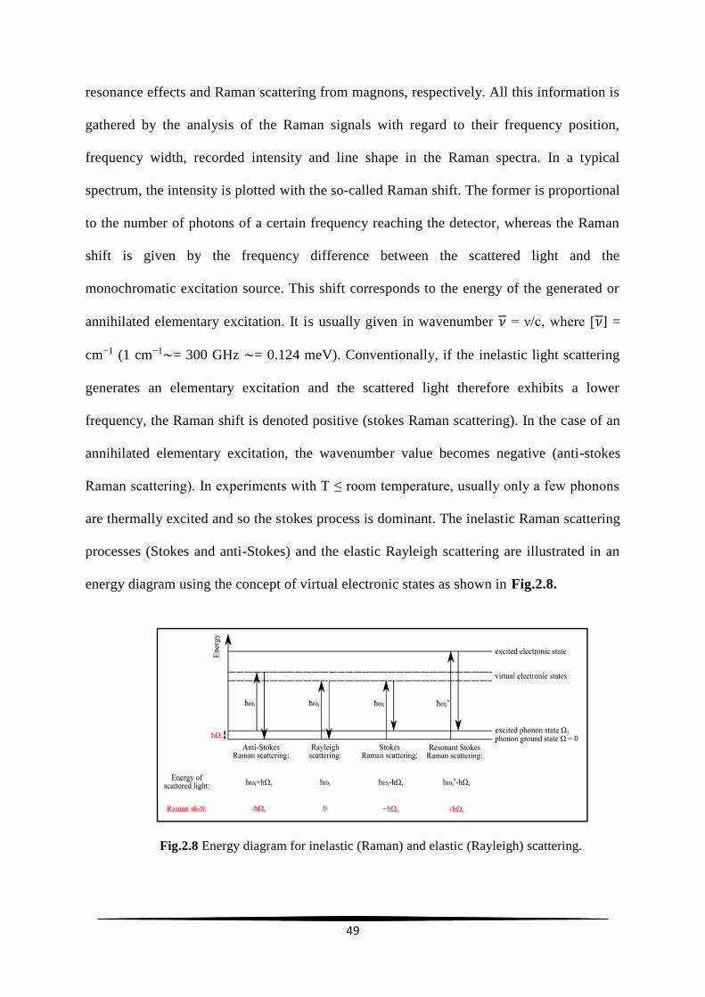
resonance effects and Raman scattering from magnons, respectively. All this information is
gathered by the analysis of the Raman signals with regard to their frequency position,
frequency width, recorded intensity and line shape in the Raman spectra. In a typical
spectrum, the intensity is plotted with the so-called Raman shift. The former is proportional
to the number of photons of a certain frequency reaching the detector, whereas the Raman
shift is given by the frequency difference between the scattered light and the
monochromatic excitation source. This shift corresponds to the energy of the generated or
annihilated elementary excitation. It is usually given in wavenumber 𝜈 = ν/c, where [𝜈] =
cm−1 (1 cm−1∼= 300 GHz ∼= 0.124 meV). Conventionally, if the inelastic light scattering
generates an elementary excitation and the scattered light therefore exhibits a lower
frequency, the Raman shift is denoted positive (stokes Raman scattering). In the case of an
annihilated elementary excitation, the wavenumber value becomes negative (anti-stokes
Raman scattering). In experiments with T ≤ room temperature, usually only a few phonons
are thermally excited and so the stokes process is dominant. The inelastic Raman scattering
processes (Stokes and anti-Stokes) and the elastic Rayleigh scattering are illustrated in an
energy diagram using the concept of virtual electronic states as shown in Fig.2.8.
Fig.2.8 Energy diagram for inelastic (Raman) and elastic (Rayleigh) scattering.

50
While in the case of resonant Raman scattering an actual electronic transition is involved,
the other Raman processes are described by the introduction of virtual electronic states. The
frequency difference between the scattered light and the monochromatic excitation source
is conventionally called Raman shift. Therefore, a Raman shift of zero corresponds to
elastic Rayleigh scattering.
General setup of Raman experiments
The general setup for Raman scattering experiments is shown in Fig.2.9 and it
consists of (i) a monochromatic light source for excitation, usually a laser, (ii) optical
equipment to bring the laser beam on the sample and collect the scattered light, (iii) a
spectrometer to analyse the scattered light and (iv) a detector to collect the signal.
Fig.2.9 Schematic experimental setup for Raman scattering experiments.
Complementary information on the sample may be derived if the exciting and
analysed light is manipulated with optical filters, polarizers, etc. Today, light sources in
Raman scattering setups are usually realized by laser systems. Gas lasers, solid-state lasers,
dye lasers and other laser devices provide a quasi-continuous variety of wavelengths from
the IR to the UV as well as continuous wave (cw) power out-puts from µW to several W.

51
Monochromatic laser light is focused on a sample; the scattered light is collected and
analysed by a spectrometer and a detector, for example a CCD. For magneto-Raman and low
temperature Raman experiments, samples are placed in a sample chamber within a liquid
helium bath or a liquid helium continuous flow cryostat. The choice of the spectrometer
setup can result in a trade-off between sensitivity and resolution. For the detection, multi-
channel detectors are essential and CCD arrays were used.
2.6.7 Optical characterisation
i) Determination of band gap energy
Intrinsic optical absorption of a single photon across the band gap is the dominant
optical absorption process in a semiconductor. When the energy of the incident photon (hν)
is larger than the band gap energy the excitation of electrons from the valence band to the
empty states of the conduction band occurs. The light passing through the material is then
absorbed and the number of electron hole pairs generated depends on the number of incident
photons S0(ν) (per unit area, unit time and unit energy). The frequency ν is related to the
wavelength λ by the relation, λ= c/ν, where c is the velocity of light. The photon flux S(x,
ν) decreases exponentially inside the crystal according to the relation,
𝑆(𝑥, 𝜈) = 𝑆0(𝜈)𝑒−𝛼𝑥 (5)
where, ‘α’ is the absorption coefficient, (α(ν) = 4πkυ/c) is determined by the absorption
process in semiconductors and ‘k’ is the extinction coefficient. For the parabolic band
structure, the relation between the absorption coefficient (α) and the band gap of the material
is given by [167],
𝛼 = 𝐴
ℎ𝜈 (ℎ𝜈 − 𝐸𝑔)𝑟 (6)
where, r = 1/2 for allowed direct transitions, r = 2 for allowed indirect transitions, r = 3 for
forbidden indirect transitions and r = 3/2 for forbidden direct transitions. ‘A’ is the

52
parameter which depends on the transition probability. The absorption coefficient can be
deduced from the absorption or transmission spectra using the relation,
𝐼 = 𝐼0𝑒−𝛼𝑡 (7)
where, ‘I’ is the transmitted intensity, ‘I0’ is the incident intensity of the light and ‘ t’ is the
thickness of the film. In the case of direct transition, (αhν)2 will show a linear
dependence on the photon energy (hν). A plot of (αhν)2 against ‘hν’ will be a straight line
and the intercept on energy axis at (αhν)2 equal to zero will give the band gap energy.
ii) Photoluminescence
Luminescence in solids is the phenomenon in which electronic states of solids
are excited by some energy from an external source and the excited states release energy as
light. When energy comes from short-wavelength light, usually UV, the phenomenon is
called photoluminescence (PL) [168]. PL is divided into two major types: Intrinsic and
extrinsic depending on the nature of electronic transition producing it.
a) Intrinsic luminescence
There are three kinds of intrinsic:
1) Band-to-band luminescence
2) Exciton luminescence
3) Cross luminescence.
Band–to–band luminescence:
Luminescence owing to the band-to-band transition occur due to the recombination of
an electron in the conduction band with a hole in the valance band, can be seen in pure
crystal at relatively high temperature. This has been observed in Si, Ge and III(B)-V(B)
compounds such as GaAs.

53
Exciton luminescence:
An exciton is a composite particle where an excited electron and a hole interact with
one another. It moves in a crystal conveying (creates) energy and produces luminescence
owing to the recombination of the electron and the hole. There are two kinds of excitons:
Wannier exciton and Frenkel exciton. The Wannier exciton model express an exciton
composed of an electron in the conduction band and a hole in the valence band bound
together by coulomb interaction. The expanse of the wave function of the electron and hole
in Wannier exciton is much larger than the lattice constant. The excitons in III(B)-V(B) and
II(B)-VI(B) compounds are examples of Wannier exciton. The Frenkel exciton model is used
in cases where expanse of electron and hole wave function is smaller than lattice constant.
The excitons in organic molecular crystals are examples of Frenkel exciton.
Cross luminescence
Cross luminescence is produced by the recombination of an electron in the valance
band with a hole created in the outer most core band. This is observed in number of alkali
and alkaline-earth halides and double halides. This takes place only when the energy
difference between the top of valance band and that of conduction band is smaller than the
band gap energy. This type of luminescence was first observed in BaF2.
b) Extrinsic luminescence
Luminescence caused by intentionally incorporated impurities, mostly metallic
impurities or defects is known as extrinsic luminescence. Most of the observed type of
luminescence of practical application belongs to this category. Intentionally incorporated
impurities are activators and materials made luminescent in this way are called phosphors.
Extrinsic luminescence in ionic crystals and semiconductors is classified into two types:
unlocalized and localized

54
Unlocalized type:
. The electrons and holes of the host lattice participate in the luminescence process of
unlocalized type. In a semiconductor, donors and acceptors act as luminescence activators.
There are two types of luminescence transitions i.e. the transition of a free carrier to a bound
carrier and the transition of a bound electron at a donor to a bound hole at an acceptor.
These kinds of luminescence lines and bands are usually observed in compound
semiconductors such as III(B)-V(B) and II(B)-VI(B) compounds.
Localised type:
In localized type the luminescence excitation and emission process are confined in a
localized luminescence centre. Various kinds of metallic impurities intentionally
incorporated in ionic crystals and semiconductors create efficient localized luminescence
centres. Localized type centres are classified into: (a) allowed transition type (b) forbidden
transition type in terms of electric dipole transitions. The electric dipole transition can take
place between energy levels with different parities. The selection rule for this transition in
atoms is ∆l= ±1. When atoms and ions are incorporated in crystals, the forbidden character
of the dipole transition is altered by the perturbation of the crystal electric field, so that the
forbidden transition becomes allowed to some degree. Many phosphors that are important
from a practical point o f v i e w are synthesized by incorporating the following activators.
a) Allowed transition type:
(i) s↔p transition–F centre↔( an electron trapped at an anion vacancy)
(ii) s2↔sp transition Tl+, Sn2+, Pb2+, Sb3+, Bi3+
(iii) f↔d transition Eu2+, Ce3+
55
b) Forbidden transition type:
(i) d↔d transition Ti3+, Cr3+, Cr2+, Mn4+, Mn2+, Fe3+, Fe2+
(ii) f↔f transition Pr3+, Nd3+, Sm3+, Eu3+, Tb3+, Tm3+ ( and other
trivalent rare earth ions)
Iron group ions show luminescence owing to the 3dn ↔ 3dn (n = 2 – 8) transition
from visible to infrared region. Among them, Cr3+ and Mn4+ ions with the 3d3
configurations and the Mn2+ ion with the 3d5 configurations are important for phosphor
application. The luminescence spectra of Mn2+ are always bands, which vary over a wide
visible range from blue to red [169]. Two types of luminescence spectra can be
distinguished: excitation and emission. In the case of an excitation spectrum the wavelength
of the exciting light is varied and the intensity of the emitted light at a fixed emission
wavelength is measured as a function of the excitation wavelength. The excitation spectrum
gives information on the position of excited states just as the absorption spectrum does,
except that the former reveals only the absorption bands that result in the emission of light.
The observed differences between the absorption and excitation spectra can yield useful
information.
An emission spectrum provides information on the spectral distribution of the light
emitted by a sample. The time resolved PL measurements are a powerful tool for the
determination of the radiative efficiency. The radiative efficiency specifies the fraction of
excited states, which de-excite by emitting photons. The emission and excitation spectra for
the powder and thin film samples are recorded using Fluorolog–3 spectroflurometer
consisting of 450W Xenon arc monochromatic lam and a CCD detector.

56
2.6.8 Electrical characterisation
i) Resistivity by two probe method
The resistivity of the films is determined by the two-probe method where the
electrodes are in planar geometry. Evaporated indium layers or high conducting silver paste
was used as the electrodes. The resistivity (ρ) of the films is calculated applying ohm’s law,
using the relation ρ = RA/L. Here ‘ R’ is the resistance given by the slope of the
current – voltage characteristic curves, ‘ A’ is the area of the film in t h e planar
geometry which is given by the product of the film thickness and the width of the film, ‘L’
is the spacing between the electrodes.
ii) Hall measurement
The electrical resistivity of a semiconductor thin film can be written using Ohm’s
law,
𝜌 = 1
𝑒𝑛𝜇 (8)
where ‘ρ’ is the film resistivity, ‘e’ is the electronic charge, ‘n’ is the number of carriers
corresponding to the carrier concentration and ‘µ’ is the carrier mobility. According to
Ohm’s law, the carrier mobility affects resistivity. Low resistivity can be achieved by
increasing the carrier concentration, mobility or both. Increasing carrier concentration is self-
limiting because at some point the increased number of free carriers decreases the mobility
of the film due to carrier scattering. Hence there is a trade- off between the carrier
density and carrier mobility for achieving low resistivity. In the case of zinc oxide films, the
resistivity (ρ), carrier concentration (n), carrier mobility (µ) and sheet resistance were
measured using four point probe in the Van der Pauw configuration [170]. Samples used
were 1cm x 1cm in size. The ohmic contacts were made using silver paste. The silver paste
was applied at the corners of the sample symmetrically as shown in Fig.2.10.

57
C D
A . . B
. .
Fig.2.10 Symmetric connections for taking the Hall measurements
Let ‘R1’ be the potential difference between ‘A’ and ‘B’ per unit current through ‘C’ and
‘D’ or vice versa. Similarly ‘R2’ the potential difference between ‘B’ and ‘C’ per unit current
through ‘D’ and ‘A’. Then sheet resistance ‘Rs’ can be calculated using the relation,
𝑅𝑠 = (𝜋
𝑙𝑛2) (
𝑅1+𝑅2
2) 𝑓 (
𝑅1
𝑅2) (9)
Where 𝑓(𝑅1 𝑅2⁄ ) is the Van der Pauw function and is given by the relation,
𝑓 (𝑅1
𝑅2) = 1 − 0.3466 (
𝑅1−𝑅2
𝑅1+𝑅2)
2 (10)
The Hall signal was measured between two ends while passing the current through the
other two ends. Hall mobility is,
𝜇 = ∆𝑅 × 108
𝐵𝑅𝑠 (11)
where ‘∆R’ is the change in resistance due to magnetic field (B), which was applied to
measure Hall voltage. Hall coefficient RH is given by,
𝑅𝐻 = 𝜇𝜌 (12)
The type of carriers can be understood from the sign of the RH. The negative values
of RH correspond to the electrons (n-type) and positive values to holes (p-type) which are
responsible for conduction.
58
iii) Nature of conductivity – Carrier type
Thermo power measurement is a useful technique for the evaluation of the type of
carriers responsible for the conduction. Thermo power measurements were carried out using
an automated set up. The set-up is similar to the one designed by Young et al [171]. The
slope of the thermo emf versus ∆T curve gives the Seebeck coefficient. A positive Seebeck
coefficient is obtained when the majority carriers are holes and a negative Seebeck
coefficient is obtained when the majority carriers are electrons. This technique is especially
useful for characterisation of type of carriers in semiconductor materials with low
mobility for charge carriers.