chapter 2b: diode and applications -...
TRANSCRIPT

1
CHAPTER 2B:
DIODE AND APPLICATIONS
D.Wilcher

2
CHAPTER 2B:
OBJECTIVES
•Analyze the operation of 3 basic types of rectifiers
•Describe the operation of rectifier filters and IC regulators
•Analyze the operation of diode limiters and clampers

3
HALF WAVE RECTIFIERS
•A rectifier is an electronic circuit that converts AC into pulsating DC.
•The voltage conversion process is known as half-wave rectification.
•When the sinusoidal input voltage goes positive, the diode is forward-biased and conducts current to the electrical load (resistor in Figure 2-15(a) )

4
FIGURE 2-15 Operation of half-wave rectifier. The diode is considered ideal.
Thomas L. Floyd and David Buchla
Fundamentals of Analog CircuitsCopyright ©2002 by Pearson Education, Inc.
Upper Saddle River, New Jersey 07458
All rights reserved.
5
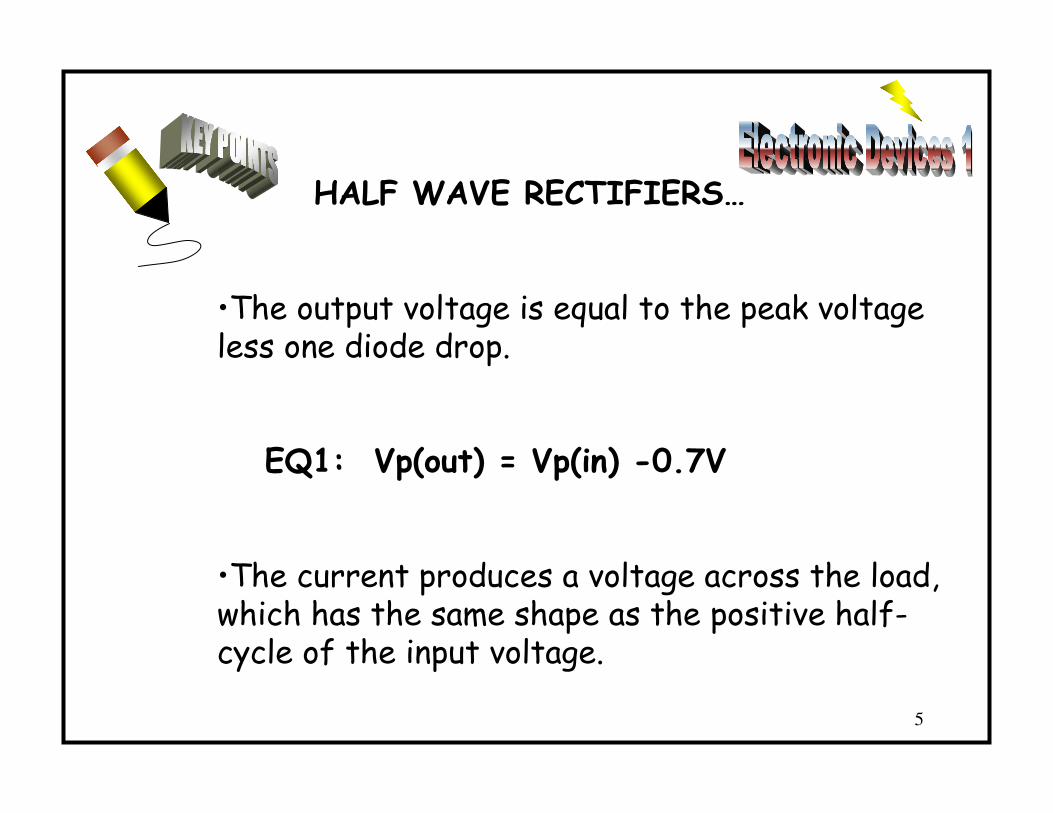
HALF WAVE RECTIFIERS…
•The output voltage is equal to the peak voltage less one diode drop.
EQ1: Vp(out) = Vp(in) -0.7V
•The current produces a voltage across the load, which has the same shape as the positive half-cycle of the input voltage.

6
HALF WAVE RECTIFIERS…
•In working with diode circuits, it is sometimes practical to neglect the diode drop when the peak value is much greater than the barrier potential.
• This analysis technique is equivalent to the using the Ideal diode model for electronic product diagnostics and validation.

7
FULL WAVE RECTIFIERS
•The difference between Full Wave and Half wave rectification is the full wave rectifier allows unidirectional current to the load during the entire input cycle.
• The half wave rectifier allows current only during one-half of the cycle.
•The result of the full wave rectification is a dc output voltage that pulsates every half cycle of the input. (See Figure 2-18.)

8
FIGURE 2-18 Full-wave rectification.
Thomas L. Floyd and David Buchla
Fundamentals of Analog CircuitsCopyright ©2002 by Pearson Education, Inc.
Upper Saddle River, New Jersey 07458
All rights reserved.

9
FIGURE 2-16
Thomas L. Floyd and David Buchla
Fundamentals of Analog CircuitsCopyright ©2002 by Pearson Education, Inc.
Upper Saddle River, New Jersey 07458
All rights reserved.

10
THE CENTER-TAPPED FULL WAVE
RECTIFIER
•The center-tapped (CT) full wave rectifier uses 2 diodes connected to the secondary of a center-tapped transformer (See Figure 2-19).
• The input signal is coupled through the transformer (AC Electronics) to the secondary.
•Half of the total secondary voltage appears between the center tap and each of the secondary windings as shown in Figure 2-19.

11
FIGURE 2-19 A center-tapped (CT) full-wave rectifier.
Thomas L. Floyd and David Buchla
Fundamentals of Analog Circuits

12
EFFECTS OF THE TURN RATIO ON
THE FULL WAVE OUTPUT VOLTAGE
•If the turns ratio of the transformer is 1, the peak value of the rectified output equals half the peak value of the primary input voltage less one diode drop.
• Value occurs because half of the input voltage appears across each half of the secondary voltage.
•In order to obtain a peak output voltage equal to the peak input voltage (less the barrier potential), a step up transformer with a turns ratio of 2 (1:2) is used.

13
PEAK INVERSE VOLTAGE
•Each diode in the full wave rectifier is alternatively forward-biased and then reversed biased.
•The maximum reverse voltage that each diode must withstand is the peak value of the total secondary voltage (Vsec).
•The peak inverse voltage either diode in the center tapped full wave rectifier is:
EQ2: PIV = Vp(out)

14
BRIDGE RECTIFIERS
•The bridge rectifier uses 4 diodes as shown in Figure 2-23.
•The most popular arrangement for power supplies because it does not require a center-tapped transformer.
•The four diodes are available in a single package, already wired in a bridge configuration.
•The bridge rectifier is a type of full wave rectifier because each half of the sine wave contributes to the output.

15
FIGURE 2-23 Operation of the full-wave rectifier. Conducting paths in the secondary are shown in color.
Thomas L. Floyd and David Buchla
Fundamentals of Analog CircuitsCopyright ©2002 by Pearson Education, Inc.
Upper Saddle River, New Jersey 07458
All rights reserved.
16
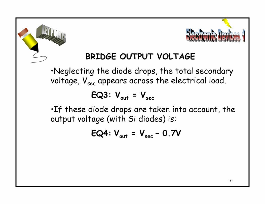
BRIDGE OUTPUT VOLTAGE
•Neglecting the diode drops, the total secondary voltage, Vsec appears across the electrical load.
EQ3: Vout = Vsec
•If these diode drops are taken into account, the output voltage (with Si diodes) is:
EQ4: Vout = Vsec – 0.7V
17
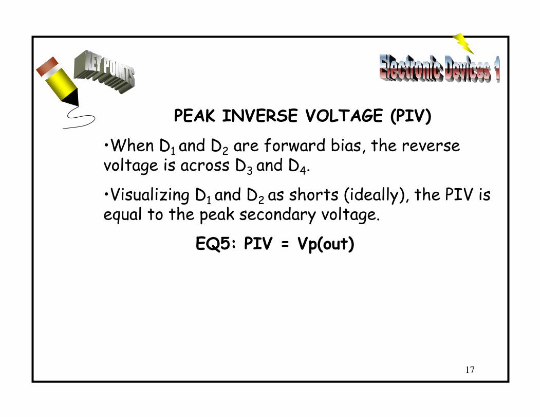
PEAK INVERSE VOLTAGE (PIV)
•When D1 and D2 are forward bias, the reverse voltage is across D3 and D4.
•Visualizing D1 and D2 as shorts (ideally), the PIV is equal to the peak secondary voltage.
EQ5: PIV = Vp(out)

18
CAPACITOR-INPUT FILTER
•A half wave rectifier with a capacitor input filter is shown in Figure 2-24.
•During the positive first quarter-cycle of the input, the diode is forward biased, allowing the capacitor to charge to within a diode drop of the input peak.
•When the input begins to decrease below its peak, the capacitor retains its charge and the diode becomes reverse bias.
•During the remaining part of the cycle and the beginning of the next cycle, the capacitor can discharge only through the load resistance at a rate determined by the RC time constant.

19
FIGURE 2-24 Operation of a half-wave rectifier with a capacitor-input filter.
Thomas L. Floyd and David Buchla
Fundamentals of Analog CircuitsCopyright ©2002 by Pearson Education, Inc.
Upper Saddle River, New Jersey 07458
All rights reserved.

20
RIPPLE VOLTAGE
•The variation in the capacitor voltage due to the charging and discharging is called the ripple voltage.
•The smaller the ripple voltage, the better the filtering action.
•For a given input frequency, the output frequency of a full wave rectifier is twice that of a half wave rectifier.
•As a result, a full wave rectifier is easier to filter because of the shorter time between peaks.

21
FIGURE 2-25 Comparison of ripple voltages for half-wave and full-wave rectifier outputs with the same filter capacitor and derived
from the same sinusoidal input.
Thomas L. Floyd and David Buchla
Fundamentals of Analog CircuitsCopyright ©2002 by Pearson Education, Inc.
Upper Saddle River, New Jersey 07458
All rights reserved.

22
SURGE CURRENT IN THE CAPACITOR
INPUT FILTER
•When the power is first applied to a power supply, the filter capacitor is uncharged..
•At the instant the switch is closed, voltage is connected to the rectifier and the uncharged capacitor appears as a short.
•This case is illustrated for a bridge circuit in Figure 2-26(a).
•An initial surge of current is produced through the forward-biased diodes.
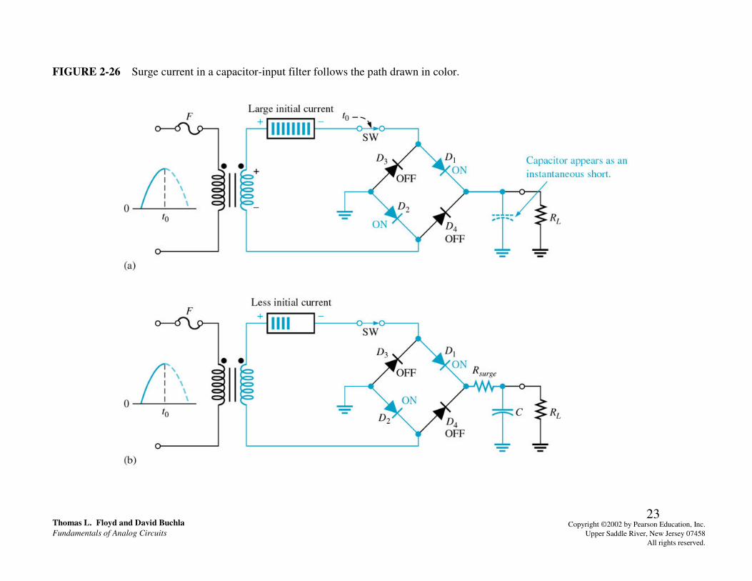
23
FIGURE 2-26 Surge current in a capacitor-input filter follows the path drawn in color.
Thomas L. Floyd and David Buchla
Fundamentals of Analog CircuitsCopyright ©2002 by Pearson Education, Inc.
Upper Saddle River, New Jersey 07458
All rights reserved.

24
SURGE CURRENT IN THE CAPACITOR
INPUT FILTER…
•It is possible that the surge current could destroy the diodes, for this reason a surge-limiting resistor Rsurge, is sometimes connected. (See Figure 2-26(b) ).
•The value of this resistor must be small to avoid a significant voltage drop across it.
•The diode must have a forward current rating that can handle the momentary surge of current.

25
IC REGULATORS
•The most effective filter is a combination of a capacitor-input filter with an IC regulator.
•In general, and IC (Integrated Circuit) is a complete functional circuit constructed on a single, tiny chip of silicon.
•An integrated circuit regulator is an IC that is connected to the output of rectifier an maintains a constant output voltage or current despite changes in the input.
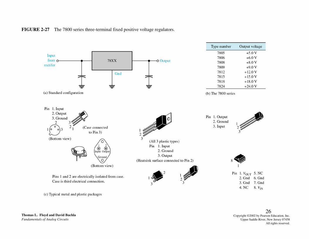
26
FIGURE 2-27 The 7800 series three-terminal fixed positive voltage regulators.
Thomas L. Floyd and David Buchla
Fundamentals of Analog CircuitsCopyright ©2002 by Pearson Education, Inc.
Upper Saddle River, New Jersey 07458
All rights reserved.

27
IC REGULATORS…
•Three terminal regulators designed for a fixed output voltage require only external capacitors to complete the regulation portion of the power (See Figure 2-27(a).
•Filtering is accomplished by a large-value capacitor between the input voltage and ground.
•Sometimes a second smaller-value input capacitor is connected in parallel, especially if the filter capacitor is not close to the IC regulator to prevent transients and internal oscillation.

28
FIGURE 2-28 A basic +5.0 V(fixed) power supply.
Thomas L. Floyd and David Buchla
Fundamentals of Analog CircuitsCopyright ©2002 by Pearson Education, Inc.
Upper Saddle River, New Jersey 07458
All rights reserved.
IC REGULATORS: 7805

29
FIGURE 2-29 A basic power supply with a variable output voltage (from 1.25 V to 6.5V).
Thomas L. Floyd and David Buchla
Fundamentals of Analog CircuitsCopyright ©2002 by Pearson Education, Inc.
Upper Saddle River, New Jersey 07458
All rights reserved.
IC REGULATORS: LM317

30
DIODE LIMITING AND CLIPPING CIRCUITS
•Diode circuits, called limiters, or clippers are sometimes used to clip off portions of the signal voltages above or below certain levels.
•Another type of diode circuit, called a clamper, is used to restore a dc level to an electrical signal.

31
DIODE LIMITERS
Diode Limiter is an electronic circuit that limits or clips off the positive or negative part of the input signal See Figures 2-30(a) and (b).
•The negative or positive signal limiting function is based on if the diode is wired in a forward or reverse biased mode .

32
FIGURE 2-30 Diode limiting (clipping circuits).
Thomas L. Floyd and David Buchla
Fundamentals of Analog CircuitsCopyright ©2002 by Pearson Education, Inc.
Upper Saddle River, New Jersey 07458
All rights reserved.

33
DETERMING VOUT
•Whenever the input is below 0.7V, the diode is reversed biased and appears as an open.
•The output voltage VOUT looks like the negative part of the input, but with a magnitude determined by the voltage divider formed by R1
and RL, as follows:
EQ5: VOUT = (RL/R1+RL)xVIN
•If R1 is small compared to RL, then VOUT≈VIN

34
DIODE CLAMPERS
•Diode Clamper adds a dc level to an ac signal.
•Clampers are sometimes known as dc restorers See Figure 2-40.
•The net effect of the clamping action is the capacitor retains a charge approximately equal to the peak value of the input less the diode drop.

35
FIGURE 2-40 Positive clamping. The diode allows the capacitor to charge rapidly. The capacitor can discharge only through R\s\do2L.
Thomas L. Floyd and David Buchla
Fundamentals of Analog CircuitsCopyright ©2002 by Pearson Education, Inc.
Upper Saddle River, New Jersey 07458
All rights reserved.