chapter 3: bridges to technology: interfaces, design rules
TRANSCRIPT
© J
. Lie
nig
, J. S
chei
ble
, Fu
nd
amen
tals
of
Layo
ut
Des
ign
fo
rEl
ectr
on
ic C
ircu
its,
Sp
rin
ger
20
20
Chapter 3: Bridges to Technology: Interfaces, Design Rules, and Libraries
3.1 Circuit Data: Schematic and Netlists
3.2 Layout Data: Layers and Polygons
3.3 Mask Data: Layout Post Processing
3.4 Geometrical Design Rules
3.5 Libraries
1
Chapter 3: Bridges to Technology: Interfaces, Design Rules, and Libraries

© J
. Lie
nig
, J. S
chei
ble
, Fu
nd
amen
tals
of
Layo
ut
Des
ign
fo
rEl
ectr
on
ic C
ircu
its,
Sp
rin
ger
20
20
Chapter 3: Bridges to Technology: Interfaces, Design Rules, and Libraries
3.1 Circuit Data: Schematics and Netlists3.1.1 Structural Description of a Circuit3.1.2 Idealizations in Circuit Descriptions3.1.3 Circuit Representations: Netlist and Schematic
3.2 Layout Data: Layers and Polygons3.2.1 Structure of Layout Data3.2.2 How to Read a Layout View3.2.3 Graphics Operations
3.3 Mask Data: Layout Post Processing3.3.1 Overview3.3.2 Chip Finishing3.3.3 Reticle Layout3.3.4 Layout-to-Mask Preparation
3.4 Geometrical Design Rules3.4.1 Technological Constraints and Geometrical Design Rules3.4.2 Basic Geometrical Design Rules3.4.3 Programmed Geometrical Design Rules3.4.4 Rules for Die Assembly
3.5 Libraries 3.5.1 Process Design Kits and Primitive Device Libraries3.5.2 Cell Libraries3.5.3 Libraries for Printed Circuit Board Design
2
Chapter 3: Bridges to Technology: Interfaces, Design Rules, and Libraries

© J
. Lie
nig
, J. S
chei
ble
, Fu
nd
amen
tals
of
Layo
ut
Des
ign
fo
rEl
ectr
on
ic C
ircu
its,
Sp
rin
ger
20
20
Chapter 3: Bridges to Technology: Interfaces, Design Rules, and Libraries
Circuit Design
Physical Designand Verification
Circuit data (Sect. 3.1)
Layout data (Sect. 3.2)
Fabrication
Specification Technology data
Layout Post Processing(Sect. 3.3)
Mask data (Sect. 3.3)
Design data
Geometricaldesign rules
(Sect. 3.4)
Libraries (Sect. 3.5)
3
© J
. Lie
nig
, J. S
chei
ble
, Fu
nd
amen
tals
of
Layo
ut
Des
ign
fo
rEl
ectr
on
ic C
ircu
its,
Sp
rin
ger
20
20
Chapter 3: Bridges to Technology: Interfaces, Design Rules, and Libraries
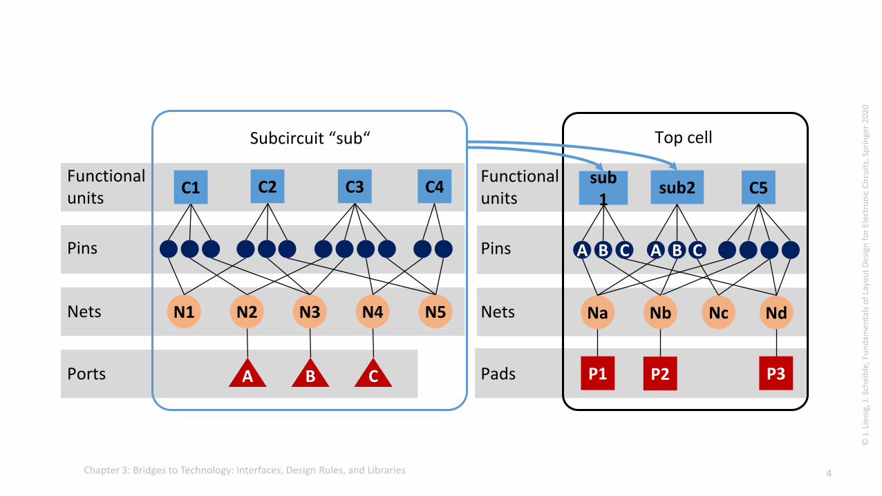
C1 C2 C3 C4
N1 N2 N3 N5N4
A B C
Functionalunits
Pins
Nets
Ports
Subcircuit “sub“
A B C A
sub1
sub2
B
Na Nb
C
C5
NdNc
Top cell
Pads
Functionalunits
Pins
Nets
P1 P2 P3
4

© J
. Lie
nig
, J. S
chei
ble
, Fu
nd
amen
tals
of
Layo
ut
Des
ign
fo
rEl
ectr
on
ic C
ircu
its,
Sp
rin
ger
20
20
Chapter 3: Bridges to Technology: Interfaces, Design Rules, and Libraries
(A: Net1)
(B: Net2)
(C: Net5)
(NAND[1]: IN1 Net1, IN2 Net2, OUT Net3)
(NAND[2]: IN1 Net1, IN2 Net2, OUT Net4)
(NOR[1]: IN1 Net3, IN2 Net4, OUT Net5)
NAND[1]
NAND[2]
NOR[1]
(Net1: A, NAND[1].IN1, NAND[2].IN1)
(Net2: B, NAND[1].IN2, NAND[2].IN2)
(Net3: NAND[1].OUT, NOR[1].IN1)
(Net4: NAND[2].OUT, NOR[1].IN2)
(Net5: NOR[1].OUT, C)
Net1
Net5
Net2
Net4
Net3
Pin-oriented netlist
Net-oriented netlist
A
B
C
5

© J
. Lie
nig
, J. S
chei
ble
, Fu
nd
amen
tals
of
Layo
ut
Des
ign
fo
rEl
ectr
on
ic C
ircu
its,
Sp
rin
ger
20
20
Chapter 3: Bridges to Technology: Interfaces, Design Rules, and Libraries
.SUBCKT bgap Ibias VDD VSS bg
QQ1 VSS VSS net05 vpnp M=1 EA=1.69
QQ0 VSS VSS net04 vpnp M=8 EA=1.69
XI0 Ibias VDD VSS net05 net01 net02 / moa
MPM1 bg net02 VDD VDD pmos W=8u L=4u M=2
MPM0 net03 net02 VDD VDD pmos W=8u L=4u M=2
RR2 net03 net05 45.05k polyhres W=2u L=255u
RR1 bg net01 45.05k polyhres W=2u L=255u
RR0 net01 net04 5.3k polyhres W=2u L=30u
.ENDS
k
k
k
6

© J
. Lie
nig
, J. S
chei
ble
, Fu
nd
amen
tals
of
Layo
ut
Des
ign
fo
rEl
ectr
on
ic C
ircu
its,
Sp
rin
ger
20
20
Chapter 3: Bridges to Technology: Interfaces, Design Rules, and Libraries
.SUBCKT moa Ibias VDD VSS inn inp outMPM4 Ibias Ibias VDD VDD pmos W=6u L=2u M=2MPM3 out Ibias VDD VDD pmos W=6u L=2u M=6MPM0 net03 inp net02 VDD pmos W=50u L=4u M=2MPM1 net01 inn net02 VDD pmos W=50u L=4u M=2MPM2 net02 Ibias VDD VDD pmos W=6u L=2u M=2MNM2 out net03 VSS VSS nmos W=12u L=2u M=6MNM1 net01 net01 VSS VSS nmos W=12u L=2u M=2MNM0 net03 net01 VSS VSS nmos W=12u L=2u M=2CC0 net03 out 635f mimcap M=2.ENDS
7

© J
. Lie
nig
, J. S
chei
ble
, Fu
nd
amen
tals
of
Layo
ut
Des
ign
fo
rEl
ectr
on
ic C
ircu
its,
Sp
rin
ger
20
20
Chapter 3: Bridges to Technology: Interfaces, Design Rules, and Libraries
C1 C2
C3C4
C5C6C7
C1 C2
C3C4
C5C6
C7
C9C10
C8
C2
C3
C4
C5C6
C7
C8
C1 C1
C2
C1
C2
C3
C4
w
(a) (b) (c) (d) (e)
8

© J
. Lie
nig
, J. S
chei
ble
, Fu
nd
amen
tals
of
Layo
ut
Des
ign
fo
rEl
ectr
on
ic C
ircu
its,
Sp
rin
ger
20
20
Chapter 3: Bridges to Technology: Interfaces, Design Rules, and Libraries
B
B
B BB
BB
C
C
c
C
c c
C
c c c
C
c c c
C
c c c
c c c c c c
C C
c c c c c c
C
c c
C
c c
C
c c
C
c c
n n
n n n n
n
n
n n
n n n nn
B
C
c
Layout block
Layout cell
Net shape (BEOL layer)
Cell shape (FEOL layer)
n
9

© J
. Lie
nig
, J. S
chei
ble
, Fu
nd
amen
tals
of
Layo
ut
Des
ign
fo
rEl
ectr
on
ic C
ircu
its,
Sp
rin
ger
20
20
Chapter 3: Bridges to Technology: Interfaces, Design Rules, and Libraries
PSD NSD
Cont
Metal1
Active Nwell
Poly
Metal1
Cont
PSD NSD Poly NwellPwell P-substrate
STI
VSS VDDOut OutIn
Layout
Sectional view
Circuit diagram
pmos
nmos
w=1.5ul=180n
w=600nl=180n
In Out
VDD
VSS
M0
M1
Cuttingline
10

© J
. Lie
nig
, J. S
chei
ble
, Fu
nd
amen
tals
of
Layo
ut
Des
ign
fo
rEl
ectr
on
ic C
ircu
its,
Sp
rin
ger
20
20
Chapter 3: Bridges to Technology: Interfaces, Design Rules, and Libraries
S/D D/SB
G
S/DD/S B
G
NMOS-FET
PMOS-FET
S/D D/SB GD/S S/D BG
Metal1
Poly
Cont
Nwell
Active
n+ (NSD)
p+ (PSD)
Metal1
Contact
PSDNSD Poly NwellPwell
P-substrate
Field oxide (FOX) = STI
Interlevel oxides (ILO)
Gate oxide (GOX)
l
w
l
w
11

© J
. Lie
nig
, J. S
chei
ble
, Fu
nd
amen
tals
of
Layo
ut
Des
ign
fo
rEl
ectr
on
ic C
ircu
its,
Sp
rin
ger
20
20
Chapter 3: Bridges to Technology: Interfaces, Design Rules, and Libraries
x = blue OR red x = blue XOR redx = blue AND red x = red ANDNOT blue x = blue ANDNOT red
Original layout
Layer “blue”
Layer “red”
Layer “x”
12

© J
. Lie
nig
, J. S
chei
ble
, Fu
nd
amen
tals
of
Layo
ut
Des
ign
fo
rEl
ectr
on
ic C
ircu
its,
Sp
rin
ger
20
20
Chapter 3: Bridges to Technology: Interfaces, Design Rules, and Libraries
Original layout
Layer “blue”
Layer “red”
INCLUDE OUTSIDE INSIDE ENCLOSE
red INCLUDE blue
blue INCLUDE red
red OUTSIDE blue
blue OUTSIDE red
red INSIDE blue
blue INSIDE red
red ENCLOSE blue
blue ENCLOSE red
red CUT blue
blue CUT red
CUT
13

© J
. Lie
nig
, J. S
chei
ble
, Fu
nd
amen
tals
of
Layo
ut
Des
ign
fo
rEl
ectr
on
ic C
ircu
its,
Sp
rin
ger
20
20
Chapter 3: Bridges to Technology: Interfaces, Design Rules, and Libraries
Sizing without beveling
2 s s
Sizing with beveling
s s
sv·s s
s
s s
14

© J
. Lie
nig
, J. S
chei
ble
, Fu
nd
amen
tals
of
Layo
ut
Des
ign
fo
rEl
ectr
on
ic C
ircu
its,
Sp
rin
ger
20
20
Chapter 3: Bridges to Technology: Interfaces, Design Rules, and Libraries
(b)
(c)
(a)
(1) Undersize (2) Oversize
Deviationfrom original
Deviationfrom original
(1) Oversize (2) Undersize
Deviationfrom original
Original
Original
15

© J
. Lie
nig
, J. S
chei
ble
, Fu
nd
amen
tals
of
Layo
ut
Des
ign
fo
rEl
ectr
on
ic C
ircu
its,
Sp
rin
ger
20
20
Chapter 3: Bridges to Technology: Interfaces, Design Rules, and Libraries
Physical Design
Chip layout data
Structures withelectrical functions
Structures withnon-electrical functions
Company logoCopyrightChip identificationLayer revision
Scribe line monitorAlignment marks
Test patterns
Mask data
Seal ring
(1)
Filler structures
(2)
(3)
Process monitor(4)
(5)
Tapeout
Reticle layout data
Grafics operations
Resolution enhancement techniques (RET)
(6)
(7)
Fracturing(8)
ReticleLayout
(Sect. 3.3.3)
Layout-to-Mask
Preparation
(Sect. 3.3.4)
Designteam
Foundry
Mask production
Layo
ut
Po
st P
roce
ssin
g
ChipFinishing
(Sect. 3.3.2)
Fabricationdata
Productdata
Productand fabricationdata
16

© J
. Lie
nig
, J. S
chei
ble
, Fu
nd
amen
tals
of
Layo
ut
Des
ign
fo
rEl
ectr
on
ic C
ircu
its,
Sp
rin
ger
20
20
Chapter 3: Bridges to Technology: Interfaces, Design Rules, and Libraries
Design region
Corner region
Seal ring
Scribe edge
Company logo Chip ID and version
Layer revisons
CX123ab
17

© J
. Lie
nig
, J. S
chei
ble
, Fu
nd
amen
tals
of
Layo
ut
Des
ign
fo
rEl
ectr
on
ic C
ircu
its,
Sp
rin
ger
20
20
Chapter 3: Bridges to Technology: Interfaces, Design Rules, and Libraries
Too mucherosion
Desirederosion
Too little erosionDishing
Metal lines homogenously spread Dummy fill structuresSlotting
Pre-CMP level(a) (b) (c) (d)
Pre-CMP level
18

© J
. Lie
nig
, J. S
chei
ble
, Fu
nd
amen
tals
of
Layo
ut
Des
ign
fo
rEl
ectr
on
ic C
ircu
its,
Sp
rin
ger
20
20
Chapter 3: Bridges to Technology: Interfaces, Design Rules, and Libraries
Die
L
ID
Die
L
ID
Die
L
ID
Die
L
ID
Die
L
ID
Die
L
ID
Die
L
ID
Die
L
ID
Die
L
ID
Scribe lines with test patterns for process monitoring
Scri
be
lines
wit
hte
stp
atte
rns
of
elec
tric
alco
mp
on
ents
Alignment marks
Logo
Layer revisions Scribe monitorstructure
19

© J
. Lie
nig
, J. S
chei
ble
, Fu
nd
amen
tals
of
Layo
ut
Des
ign
fo
rEl
ectr
on
ic C
ircu
its,
Sp
rin
ger
20
20
Chapter 3: Bridges to Technology: Interfaces, Design Rules, and Libraries
Layout Post Process A
Layout data Mask data
NSD Active
Polyn-Active p-Active
PSD Active
Nwell
Layout Post Process B
20

© J
. Lie
nig
, J. S
chei
ble
, Fu
nd
amen
tals
of
Layo
ut
Des
ign
fo
rEl
ectr
on
ic C
ircu
its,
Sp
rin
ger
20
20
Chapter 3: Bridges to Technology: Interfaces, Design Rules, and Libraries
PolyRes
.RES
Polyres
(a) (b) (c)
Text Poly
21

© J
. Lie
nig
, J. S
chei
ble
, Fu
nd
amen
tals
of
Layo
ut
Des
ign
fo
rEl
ectr
on
ic C
ircu
its,
Sp
rin
ger
20
20
Chapter 3: Bridges to Technology: Interfaces, Design Rules, and Libraries
Design RuleRelationship between
edgesNumber of
shapesNumber of
layers
Width Inside / inside 1 1
Spacing Outside / outside(a) 1 or 2(b) 2
(a) 1(b) 2
Extension Inside / outside 2 2
Intrusion Inside / inside 2 2
Enclosure Outside / inside 2 2
22

© J
. Lie
nig
, J. S
chei
ble
, Fu
nd
amen
tals
of
Layo
ut
Des
ign
fo
rEl
ectr
on
ic C
ircu
its,
Sp
rin
ger
20
20
Chapter 3: Bridges to Technology: Interfaces, Design Rules, and Libraries
Width
Designrule
checked
Spacing Extension Intrusion Enclosure
Designrulenot
checked
No errors can occur
23
© J
. Lie
nig
, J. S
chei
ble
, Fu
nd
amen
tals
of
Layo
ut
Des
ign
fo
rEl
ectr
on
ic C
ircu
its,
Sp
rin
ger
20
20
Chapter 3: Bridges to Technology: Interfaces, Design Rules, and Libraries
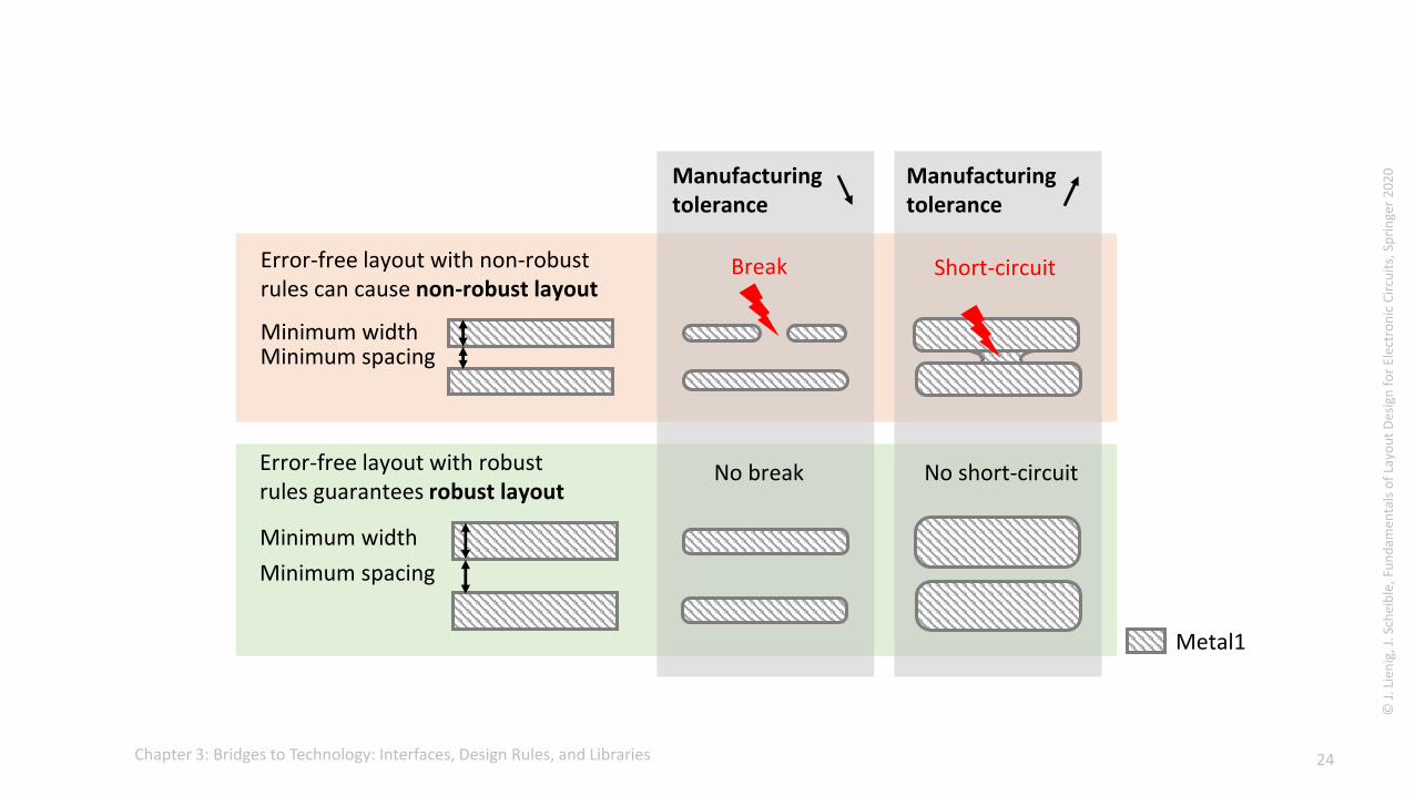
Metal1
Short-circuit
Manufacturing tolerance
BreakError-free layout with non-robust rules can cause non-robust layout
Minimum width
Minimum spacing
Manufacturing tolerance
No short-circuitNo break
Minimum widthMinimum spacing
Error-free layout with robust rules guarantees robust layout
24

© J
. Lie
nig
, J. S
chei
ble
, Fu
nd
amen
tals
of
Layo
ut
Des
ign
fo
rEl
ectr
on
ic C
ircu
its,
Sp
rin
ger
20
20
Chapter 3: Bridges to Technology: Interfaces, Design Rules, and Libraries
Active NSD Poly Cont Metal1
Misaligned Poly mask
Source to drain short
Misaligned Metal1 mask
Bad/missing contacts
Misaligned NSD mask
Short between S/Dand p-substrate
Error-free layout with non-robustrules can cause non-robust layout
Enclosure NSD Active
Enclosure Metal1 Cont
No short No short Good contacts
Extension Poly Active
Error-free layout with robustrules guarantees robust layout
25

© J
. Lie
nig
, J. S
chei
ble
, Fu
nd
amen
tals
of
Layo
ut
Des
ign
fo
rEl
ectr
on
ic C
ircu
its,
Sp
rin
ger
20
20
Chapter 3: Bridges to Technology: Interfaces, Design Rules, and Libraries
X1 = Active ANDNOT Poly X2 = X1 ANDNOT Cont X3 = SIZE (X2, -clear) Result = SIZE (X3, +clear)
Active NSD Poly Cont Metal1Physical layers: Calculated layers: X1 X2 X3 Result
26

© J
. Lie
nig
, J. S
chei
ble
, Fu
nd
amen
tals
of
Layo
ut
Des
ign
fo
rEl
ectr
on
ic C
ircu
its,
Sp
rin
ger
20
20
Chapter 3: Bridges to Technology: Interfaces, Design Rules, and Libraries
Mold compoundBonding wire
Die Lead frame
Package leads
27

© J
. Lie
nig
, J. S
chei
ble
, Fu
nd
amen
tals
of
Layo
ut
Des
ign
fo
rEl
ectr
on
ic C
ircu
its,
Sp
rin
ger
20
20
Chapter 3: Bridges to Technology: Interfaces, Design Rules, and Libraries
Lead frame
Bonding wire
Bonding-wire angle
Forbidden area for bond pads
Bond pad
Contact points on the lead frame
28

© J
. Lie
nig
, J. S
chei
ble
, Fu
nd
amen
tals
of
Layo
ut
Des
ign
fo
rEl
ectr
on
ic C
ircu
its,
Sp
rin
ger
20
20
Chapter 3: Bridges to Technology: Interfaces, Design Rules, and Libraries
OUTIN1
VDD
GND
IN2
IN1
IN2OUT
architecture RTL of NOR2 is
begin
OUT <= NOT(IN1 OR IN2);
end architecture RTL;
entity NOR2 is
port(IN1: in std_logic;
IN2: in std_logic;
OUT: out std_logic)
end entity NOR2;
SymbolModel
Layout
29

© J
. Lie
nig
, J. S
chei
ble
, Fu
nd
amen
tals
of
Layo
ut
Des
ign
fo
rEl
ectr
on
ic C
ircu
its,
Sp
rin
ger
20
20
Chapter 3: Bridges to Technology: Interfaces, Design Rules, and Libraries
SimulationSchematicEntry
Layout Design
Primitive device library
Layout Verification
Layers
LVS
DRC
ERC
PEXSymbol Model Layout
Process design kit (PDK)
Layout data
30

© J
. Lie
nig
, J. S
chei
ble
, Fu
nd
amen
tals
of
Layo
ut
Des
ign
fo
rEl
ectr
on
ic C
ircu
its,
Sp
rin
ger
20
20
Chapter 3: Bridges to Technology: Interfaces, Design Rules, and Libraries
D-type flip flop w/ reset: D_FF_RD-type flip flop w/ reset/set: D_FF_RSD-type flip flop w/ reset andscan input: D_FF_R_SCD-type latch w/ reset: LD_RD-type latch w/ reset and scaninput: LD_R_SCBus keeper flip flop: BK
NAND gate: NAND2, NAND3 …NOR gate: NOR2, NOR3 …AND gate: AND2OR gate: OR2Inverter: INV, INV_2X, INV_4XBuffer: BUF_4X, BUF_16X …Tristate buffer: TRI_BUF_8XXOR gate: XOR2Multiplexer: MUX21, MUX41
SimulationLogicSynthesis
Layout Design
Layout Verification
Combinatorial (gates) Memory (flip flops, latches)
Standard cell library
Symbol Model Layout
LVS
DRC
ERC
PEX
Layout data
31

© J
. Lie
nig
, J. S
chei
ble
, Fu
nd
amen
tals
of
Layo
ut
Des
ign
fo
rEl
ectr
on
ic C
ircu
its,
Sp
rin
ger
20
20
Chapter 3: Bridges to Technology: Interfaces, Design Rules, and Libraries
Symbol library name
Symbols in this library
Selected symbol
Symbol editor
Pin names, pin assignment
Reference to footprint
32

© J
. Lie
nig
, J. S
chei
ble
, Fu
nd
amen
tals
of
Layo
ut
Des
ign
fo
rEl
ectr
on
ic C
ircu
its,
Sp
rin
ger
20
20
Chapter 3: Bridges to Technology: Interfaces, Design Rules, and Libraries
Footprint library name
Footprints in this library
Footprint editor
Selected footprint
Constituting elementsof the footprint
33

© J
. Lie
nig
, J. S
chei
ble
, Fu
nd
amen
tals
of
Layo
ut
Des
ign
fo
rEl
ectr
on
ic C
ircu
its,
Sp
rin
ger
20
20
Chapter 3: Bridges to Technology: Interfaces, Design Rules, and Libraries
Model name
Model category (diode)
Device specific parameter set
34