chapter 6: aerospace and defense - ieee · 2019-10-03 · chapter 15: materials and ... challenges,...
TRANSCRIPT

2019 Edition
Chapter 6: Aerospace and Defense
http://eps.ieee.org/hir
We acknowledge with gratitude the use of material and figures in this Roadmap that are excerpted from original sources. Figures & tables should be re-used only with the permission of the original source.
The HIR is devised and intended for technology assessment only and is without regard to any commercial considerations pertaining to individual products or equipment.

October, 2019 Table of Contents
HIR Version 1.0 (eps.ieee.org/hir) Page ii Heterogeneous Integration Roadmap
Table of Contents
CHAPTER 1: HETEROGENEOUS INTEGRATION ROADMAP: OVERVIEW .......................................................................... 1
CHAPTER 2: HIGH PERFORMANCE COMPUTING AND DATA CENTERS ............................................................................. 1
CHAPTER 3: THE INTERNET OF THINGS (IOT) .................................................................................................................. 1
CHAPTER 4: MEDICAL, HEALTH & WEARABLES ............................................................................................................... 1
CHAPTER 5: AUTOMOTIVE ............................................................................................................................................ 1
CHAPTER 6: AEROSPACE AND DEFENSE ......................................................................................................................... 1 1. EXECUTIVE SUMMARY ............................................................................................................................................................ 1 2. HIR AEROSPACE‐DEFENSE WORKING GROUP ............................................................................................................................. 1 3. INTRODUCTION AND MOTIVATION ............................................................................................................................................ 2 4. WHAT IS THE AEROSPACE AND DEFENSE SECTOR?........................................................................................................................ 4 5. IMPACT OF HETEROGENEOUS INTEGRATION ON AEROSPACE AND DEFENSE SYSTEMS .......................................................................... 5 6. WHAT IS HETEROGENOUS INTEGRATION .................................................................................................................................... 6 7. 2.5D HETEROGENEOUS INTEGRATION PROGRESS ........................................................................................................................ 7 8. 3D HETEROGENEOUS INTEGRATION ........................................................................................................................................ 17 9. OUTLOOK FOR NEXT 5 TO 10 YEARS ........................................................................................................................................ 19 10. DARPA ELECTRONICS RESURGENCE INITIATIVE (ERI) ............................................................................................................... 21 11. SUPPLY CHAIN ................................................................................................................................................................... 22
CHAPTER 7: MOBILE ...................................................................................................................................................... 1
CHAPTER 8: SINGLE CHIP AND MULTI CHIP INTEGRATION .............................................................................................. 1
CHAPTER 9: INTEGRATED PHOTONICS ........................................................................................................................... 1
CHAPTER 10: INTEGRATED POWER ELECTRONICS .......................................................................................................... 1
CHAPTER 11: MEMS AND SENSOR INTEGRATION ........................................................................................................... 1
CHAPTER 12: 5G COMMUNICATIONS ............................................................................................................................. 1
CHAPTER 13: CO DESIGN FOR HETEROGENEOUS INTEGRATION ..................................................................................... 1
CHAPTER 14: MODELING AND SIMULATION .................................................................................................................. 1
CHAPTER 15: MATERIALS AND EMERGING RESEARCH MATERIALS ................................................................................. 1
CHAPTER 16: EMERGING RESEARCH DEVICES ................................................................................................................ 1
CHAPTER 17: TEST TECHNOLOGY ................................................................................................................................... 1
CHAPTER 18: SUPPLY CHAIN .......................................................................................................................................... 1
CHAPTER 19: SECURITY ................................................................................................................................................. 1
CHAPTER 20: THERMAL ................................................................................................................................................. 1
CHAPTER 21: SIP AND MODULE SYSTEM INTEGRATION ................................................................................................. 1
CHAPTER 22: INTERCONNECTS FOR 2D AND 3D ARCHITECTURES ................................................................................... 1
CHAPTER 23: WAFER‐LEVEL PACKAGING (WLP) ............................................................................................................. 1
To download additional chapters, please visit
http://eps.ieee.org/hir

June, 2019 Aerospace and Defense
HIR version 1.0 Chapter 6, Page 1 Heterogeneous Integration Roadmap
Chapter 6: Aerospace and Defense
1. Executive Summary
The Aerospace and Defense segment of the semiconductor industry has unique needs in terms of technology, security, supply chain, and lifecycle. Heterogeneous integration is a critical technology that intersects all of these challenges, so a Heterogeneous Integration Roadmap (HIR) that specifically targets the unique requirements of Aerospace and Defense is needed. This Roadmap identifies challenges in 5-, 10-, and 15-year horizons and provides guidance on how to meet those challenges. This is, of course, a perpetual work-in-progress and will be updated as capabilities move forward and new requirements arise.
Initial Scope
This initial version of the A&D chapter is focused largely on challenges and requirements for the U.S. Aerospace and Defense Industry. The intent of the Heterogeneous Integration Roadmap is to create a document that provides guidance that is useful to the semiconductor community around the world, so the US-centric viewpoint should be seen as just the starting point for this work. There are certainly many technical challenges that are pervasive throughout the international A&D industry, such as reliability, bandwidth, thermal management, radiation hardening, long product development cycles and lifetime, and supply chain security, so much of the content can be generalized beyond the US Aerospace and Defense Industry. Future revisions of this chapter will reflect that broader scope.
2. HIR Aerospace-Defense Working Group
2.1 Mission Statement for Aerospace – Defense TWG
The mission of the HIR Technology Working Group (TWG) for Aerospace and Defense (A-D) is to identify challenges, provide guidance, and recommend solutions to the A-D profession (industry, academia, and government) with sufficient lead time that they do not become roadblocks that prevent the continued implementation of leading-edge electronics in Aerospace and Defense systems.
There is the need to address heterogeneous integration technologies for new capabilities for embedded high-speed computing, cyber, sensors, C4ISR, signal processing, radar, and RF/analog, all while addressing unique constraints and requirements, such as security, reliability, small production volumes, and long lifecycle timelines. That progress is essential to the future growth of the industry and the realization of the promise of continued impact on aerospace, defense and security applications.
The approach is to identify the requirements for heterogeneous integration in the A-D electronics industry with 5-, 10- and 15-year horizons, determine the difficult challenges that must be overcome to meet these requirements and, where possible, identify potential solutions and synergies between the greater commercial sectors and the smaller A-D community.
2.2 The TWG for Developing the Heterogeneous Integration Roadmap for Aerospace and Defense
The Goal for the A-D TWG is to develop a roadmap for heterogeneously integrated components for applications in the Aerospace and Defense sector which want to leverage heterogeneous integration technologies that are available in the commercial marketplace but with special needs and challenges.
Specific goals: Identify the A-D–specific challenges in the next 5, 10 and 15 year horizons Identify promising solutions and technologies Identify any unaddressed challenges and the types of solutions/technologies needed Document all of these as a chapter in the overall HIR document Continue monitoring and analyzing the A-D semiconductor and packaging space to update the roadmap
in the next version of the HIR Much of the content of this initial version of the A&D chapter is on 2.5D integration technologies,
largely because of the industry's progress and focus on 2.5D, as well as significant overlap with commercial 2.5D approaches. We anticipate that future revisions will add significant content on 3D integration and other approaches such as wafer-level fan-out as A&D requirements evolve and multiple solutions are needed.

June, 2019 Aerospace and Defense
HIR Version 1.0 Chapter 6, Page 2 Heterogeneous Integration Roadmap
3. Introduction and Motivation
For over 70 years, the US government (USG) has worked closely with the semiconductor industry to help foster the semiconductor ecosystem to what it is today. In the early years before the mass proliferation of consumer electronic devices, the government was the primary driver of technology. Many of the available technologies originated in USG-funded research and development (R&D) programs. Prominent examples include printed circuit boards, GaAs devices, micro-electro-mechanical systems (MEMS), the fundamental technology of the internet, global positioning systems (GPS), and much of the technology needed for 5G. Funding for development of transistors and then ICs in the ‘50’s and ‘60’s, with the USG as the primary initial customer, resulted in the moon landing 50 years ago. In recent years, commercial applications such as personal computers, mobile devices, and now the Internet of Things (IoT) have created an enormous production demand and business opportunity that is the primary focus of the semiconductor industry. As a result, microelectronics for A-D needs is a small fraction of the total semiconductor market and therefore has a diminished impact on industry roadmaps.
From an Aerospace-Defense (A-D) perspective, having a continued access to advanced semiconductor technology is important not only for national defense but for the country’s economic vitality. In the recent US President’s Council of Advisors on Science and Technology (PCAST) report, it states:
“The global semiconductor market has never been a completely free market: it is founded on science that historically has been driven, in substantial part, by government and academia; segments of it are restricted in various ways as a result of national-security and defense imperatives; and it is frequently the focus of national industrial policies. Market forces play a central and critical role. But any presumption by U.S. policymakers that existing market forces alone will yield optimal outcomes – particularly when faced with substantial industrial policies from other countries – is unwarranted.”1
3.1 National Defense Strategy (2018)2
The USG’s National Defense Strategy was published in 2018. Key take-aways that highlight challenges include: “Platform electronics and software must be designed for routine replacement instead of static
configurations that last more than a decade” and must also “Deliver performance at the speed of relevance.”
“New commercial technology will change society and, ultimately, the character of war. The fact that many technological developments will come from the commercial sector means that state competitors and non-state actors will also have access to them, a fact that risks eroding the conventional overmatch to which our Nation has grown accustomed.”
Modern warfare is increasingly dependent on microelectronics capabilities that sense the environment, convert the
signals into data streams, process the information, and generate a response. In this sense, A-D systems are quite similar to commercial systems that perform communications and computations, while taking advantage of the advancement of semiconductor density, functionality, and cost reduction due to Moore’s Law. There is the ever-increased demand for more data throughput through wired and wireless systems. Cellular systems have migrated from 3G to 4G and now 5G architectures which improves bandwidth ~10X with each generation. DoD systems for communications, radar, and sensing generally require wider bandwidths, higher dynamic range, and higher transmit power, as well as specialized frequency bands and security requirements that the commercial side does not require. Figure 3-2 highlights the direction of the next generation of warfare and enabling systems for a system-of-systems framework. The challenges in the A-D space overlap those in the commercial world but extend beyond those as noted above.
1 https://obamawhitehouse.archives.gov/sites/default/files/microsites/ostp/PCAST/pcast_ensuring_long-
term_us_leadership_in_semiconductors.pdf 2 2018 National Defense Strategy found at https://dod.defense.gov/Portals/1/Documents/pubs/2018-National-Defense-
Strategy-Summary.pdf

June, 2019 Aerospace and Defense
HIR Version 1.0 Chapter 6, Page 3 Heterogeneous Integration Roadmap
Figure 3-1. US DoD funding historical perspective3
Figure 3-2. Notional future warfighting systems architecture
3 https://www.semiwiki.com/forum/content/7368-meeting-challenges-national-defense-strategy.html

June, 2019 Aerospace and Defense
HIR Version 1.0 Chapter 6, Page 4 Heterogeneous Integration Roadmap
3.2 NDIA Trusted Microelectronics Study
In 2017, the National Defense Industrial Association (NDIA) conducted a study of Trusted Microelectronics which resulted in the following recommendations for action.4
Create a U.S. National Semiconductor Strategy “The absence of a comprehensive national semiconductor strategy was viewed … as a major impediment to
assuring access to critical national security technologies and to U.S. technological competitiveness.” Adapt DoD Acquisition Practices to Align with Commercial Market Noting the “differences between DoD’s acquisition practices and commercial sales priorities,” the report
“recommends defense programs be provided new methods to purchase technology on commercial terms after the commercial products have been evaluated for trustworthiness.”
Increase DoD Market Influence Since “the DoD’s share of the semiconductor market has dramatically declined to less 1% share of today’s
semiconductors consumption and the Department’s ability to gain access to needed microelectronics capabilities has correspondingly diminished, … increase market influence by exchanging research investment for access to commercial products; and, aggregating demand across DoD programs, other USG offices, and non-USG industries that have similar component and system integrity concerns.”
Adopt New Trust and Assurance Models “Defining the boundaries for assurance spectrums or ‘tiers of trust’ levels, and would cover component categories
beyond ASICs.” Launch R&D to Achieve Trust/Security in Un-trusted Fabs “Launching near-term research and development to address the security concerns of existing commercial
technology capabilities, including Trusted 3D/2.5D integration, to leverage these capabilities for defense systems.” Two of the four NDIA Trusted Microelectronics Joint Working Groups (TM JWGs) studied the microelectronics
landscape and made recommendations that relate to heterogenous integration. NDIA TM JWG Team 1 addressed the Future Needs & System Impact of Microelectronics Technologies, asking the following questions.5
“What are the future microelectronics capabilities needed by defense contractors to maintain our technical advantage?”
“Are there new hardware paradigms on the horizon that could be disruptive?” SYSTEMS: System Needs and System Capabilities: What are the future requirements for DoD
Systems? ENABLING COMPONENTS: What are the emerging technologies enabling these capabilities
at the component level? ADOPTION: What are the risks regarding secure component availability (5-10 years) that
enables system capabilities? The HIR A-D chapter will attempt to ask similar questions and suggest some insight that pertains to Heterogeneous
Integration for this community.
4. What is the Aerospace and Defense Sector?
Deloitte in its 2019 Global Aerospace and Defense Industry Outlook white paper6 makes the following observations:
The commercial aircraft order backlog is at its peak of more than 14,000, with about 38,000 aircraft expected to be produced globally over the next 20 years.
Resurgence of global military spending as geopolitical risks increase worldwide.
4 http://www.ndia.org/-/media/sites/ndia/divisions/working-groups/tmjwg-documents/tm-jwg-esr-v3.ashx?la=en 5 http://www.ndia.org/-/media/sites/ndia/divisions/working-groups/tmjwg-documents/ndia-tm-jwg-team-1-white-paper-
finalv3.ashx?la=en 6 Deloitte 2019 Global aerospace and defense industry outlook, found at
https://www2.deloitte.com/global/en/pages/manufacturing/articles/global-a-and-d-outlook.html

June, 2019 Aerospace and Defense
HIR Version 1.0 Chapter 6, Page 5 Heterogeneous Integration Roadmap
Space is becoming an important part of the defense ecosystem as warfare moves into the domain of space assets such as satellites for military operations including surveillance, communications and targeting.
Changes in international trade agreements are likely to disrupt the global supply chain and increase costs.
Although the USA dominates in A-D spending and revenue generation, other key regions are expected to contribute to the sector including China, France, India, Japan, the Middle East and the United Kingdom.
The Aerospace and Defense sector has been at the forefront of digital innovations, leading the way for other industries in the adoption of technologies. 7 The hierarchy can be shown as:
End Customers (e.g., USG). System Primes (OEMs) who provide end-to-end system solution to the end-users. Subsystem Suppliers who provide vital subsystems including propulsion, command and control,
electronic warfare, and structural subsystems to the Primes. Component Suppliers provide component parts including energetic and structural materials,
microelectronics, cables, and connectors for prime and major subsystem providers. Pure Play Suppliers (materials, equipment, design, manufacturing, services to other supply chain
players). Figure 4-1. highlights the differences between the Commercial and Aerospace-Defense business models.
Commercial products have very short lifecycles, whereas A-D products must be supported for decades. The cost of engineering for commercial products can be amortized over millions or billions of units whereas A-D products may be in the thousands, hundreds or lower. A-D Systems are generally insensitive to unit costs but they must operate in extreme environments and have demonstrated pedigree that is tracked over the product lifecycle.
Figure 4-1. Differences between the commercial and aerospace – defense business models8
5. Impact of Heterogeneous Integration on Aerospace and Defense Systems
Several characteristics of the A-D sector create unique challenges:
7 REPORT TO CONGRESS: Fiscal Year 2016 Annual Industrial Capabilities, found at
https://www.businessdefense.gov/Portals/51/Documents/Resources/2016%20AIC%20RTC%2006-27-17%20-%20Public%20Release.pdf?ver=2017-06-30-144825-160
8 NDIA: Trusted Microelectronics Joint Working Group: Future Needs & System Impact of Microelectronics Technologies, found at http://www.ndia.org/divisions/working-groups/tmejwg/final-team-reports
June, 2019 Aerospace and Defense
HIR Version 1.0 Chapter 6, Page 6 Heterogeneous Integration Roadmap
High Performance – Need access to leading silicon nodes and advanced packaging technologies to
maintain advantage in specific technical metrics (e.g., digitization over wide bandwidths and at high dynamic range)
High Reliability – Need to survive in harsh environments, prioritize human safety in high-risk environment
Long Product Lifecycles – Need to manage parts obsolescence and upgradability Low Volumes – Need access to supply chain that provides high product mix, and business models where
NRE is managed without high volumes for amortization Security – Need secure domestic supply chain and/or verification technologies
Heterogeneous integration is a factor in all of these challenges, whether by adding new twists to the challenges with multiple device technologies or by solving some of them with modular designs and assemblies. Most specifically, heterogeneous integration directly addresses the high-performance challenge for the A-D sector. Monolithic System on a Chip solutions are becoming increasingly limited for A-D applications. Sustaining Moore’s Law by increasing the core count on a die is not feasible as memory access bottlenecks prevail and die size and complexity become prohibitively expensive. Diversity in process nodes and materials are needed (CPUs, GPUs, FPGAs) for enhancing performance, energy efficiency and programmability. Similarly, RF/mm-wave devices and data converters are needed for communications and sensing. Heterogeneous integration offers a way to address these limitations and sustain Moore’s Law through interconnect length reductions and optimal combinations of different device technologies. The A-D sector must adapt and adopt innovation and market drivers from the commercial semiconductor industry.
What are metrics to consider?
There are numerous metrics to consider for heterogeneous integration in the A-D sector, and they can vary by application (communications, radar, EW, etc.). Categorized metrics include:
Performance: data rate, latency, TFLOPs, insertion loss, isolation, dynamic range Energy/Power: energy per bit, TFLOPS/Joule, leakage power Interfaces: signaling protocols, error correction, interconnect lengths, ESD Thermal: maximum junction temperature, total device power, device power density, hot spot power
density, thermal test standards Electrical: power distribution losses to components inside package, losses in conversion, peak inductive
noise, harmonic noise Reliability/Availability: MTBF, radiation hardness, metric related to graceful degradation on component
failures, product lifetime (driving component availability)
6. What is Heterogenous Integration
(Refer to other HIR Chapters by reference to the definition of 2D, 2.1D, 2.5D and 3D heterogeneous integration). Figure 6-1 shows the 3-D IC classifications, comparing wafer-to-wafer, die-to-die and monolithic device-to-device
levels of heterogenous integration. Within the A-D community, the advantages of higher logic densities and mixing/matching CMOS ICs from different technology nodes are very attractive.
The A-D component and sub-systems can benefit from the well-stated benefits of heterogeneous Integration at all levels. In this chapter, the focus is on 2.5D integration, since many 2D and 2.1D integrations and solutions are already in wide use. Chip-and-wire assembly is a standard process. Wafer-level and fan-out packages, although attractive for high-volume applications and miniaturization, may not be sufficient for high performance and harsh environments. 2.5D technology, which is represented by High Bandwidth Memory (HBM) and other applications with stacked devices on organic substrates or silicon interposers, is attractive for A-D since this approach enables higher performance and high-density integration while leveraging conventional technology building blocks.
In many ways, the A-D users have similar needs as the HPC use case. Therefore, it is recommended that A-D users leverage capabilities and supply chain partners from the HPC ecosystem (Figure 6-2).

June, 2019 Aerospace and Defense
HIR Version 1.0 Chapter 6, Page 7 Heterogeneous Integration Roadmap
Figure 6-1. 2.5D Heterogeneous Integration is the main focus of this A-D chapter
Figure 6-2. “2.5D” and 3DIC are widely used by high performance computing
7. 2.5D Heterogeneous Integration Progress
Heterogeneous integration via 2.5D technology is approaching mainstream status, with industry leaders such as Xilinx, Intel, Nvidia, and AMD using it in their leading products. They have identified the benefits of splitting up silicon functionality, whether to improve yield with smaller chips, as Xilinx did with their pioneering FPGA “slices,” or to enable the integration of different types of devices. To summarize:
Chiplets (smaller pieces of silicon) will enable their silicon architects to ship more powerful processors more quickly.9
Modularity facilitates shorter time-to-market to mix and match different chiplets linked by shorter data interconnections, instead of implementing new complex SOC designs for the entire system.
2.5D can reduce design costs and risk by having a larger portion of the design composed of reused IP blocks that are assembled on an interposer rather than integrated in a new IC design.
Notable industry leaders see this trend. AMD’s Mark Papermaster said “I think the whole industry is going to be moving in this direction.” Similarly, Intel’s technologists see that same thing. Ramune Nagisetty, a senior principal engineer at Intel, calls it “an evolution of Moore’s law.”
9 Found at https://www.wired.com/story/keep-pace-moores-law-chipmakers-turn-chiplets/

June, 2019 Aerospace and Defense
HIR Version 1.0 Chapter 6, Page 8 Heterogeneous Integration Roadmap
DARPA has led the way in advancing Heterogeneous Integration Technology through a number of programs, as shown in Figure 7-1 and Figure 7-2. The DARPA DAHI program demonstrated the feasibility of 2.5D HI for integration of CMOS devices with high-performance III-V devices through both die-to-wafer and wafer-to-wafer bonding techniques. The DARPA CHIPS program (which is still on-going) is developing a 2.5D chiplet ecosystem and a set of standard interfaces for chiplet to chiplet communications.
Figure 7-1. DARPA’s history of integration innovation
Figure 7-2. DARPA heterogeneous integration 10
10 Daniel Green, “DARPA’s CHIPS Program and Making Heterogenous Integration Common,” 3D-ASIP 2017, 6
December 2017

June, 2019 Aerospace and Defense
HIR Version 1.0 Chapter 6, Page 9 Heterogeneous Integration Roadmap
7.1 DARPA DAHI Program
Daniel Green reported on the Progress and Prospects of Heterogeneous Integration at DARPA and summarized the progress made on a number of programs.11
The Diverse Accessible Heterogeneous Integration (DAHI)12 Foundry Technology program was designed to establish an accessible, manufacturable technology for device-level heterogeneous integration of a wide array of materials and devices (including, for example, multiple electronics and MEMS technologies) with complex silicon-enabled (e.g., CMOS) architectures on a common silicon substrate. This program culminated in accessible foundry processes of DAHI technology and demonstrations of advanced microsystems with innovative architectures and designs that leverage heterogeneous integration. By enabling the ability to ‘mix and match’ a wide variety of devices and materials on a common silicon substrate, circuit designers can select the best device for each function within their designs. This integration would provide DoD systems with the benefits of a variety of devices and materials integrated in close proximity on a single chip, minimizing the performance limitations caused by physical separation among devices.
Some of the key results are summarized in Figures 7-3, 7-4, 7-5, 7-6 and 7-7 below. The program demonstrated capabilities that would not have been possible in monolithic implementations, while uncovering several challenges in design, fabrication, and assembly along the way. The DAHI program has served as the baseline for heterogeneous integration at DARPA and beyond in the DoD.
Figure 7-3. DAHI demonstrates CMOS to III-V IC integration using 2.5D techniques
11 Daniel Green, “Progress and Prospects of Heterogeneous Integration at DARPA,” found at
http://www.meptec.org/Resources/6%20-%20Green.pdf 12 DARPA DAHI Program: https://www.darpa.mil/program/dahi-foundry-technology

June, 2019 Aerospace and Defense
HIR Version 1.0 Chapter 6, Page 10 Heterogeneous Integration Roadmap
Figure 7-4. DARPA DAHI technologies addressed high-performance RF performance and integration of CMOS digital functions
Figure 7-5. DARPA DAHI used DBI process to achieve transistor-level integration with Si CMOS and InP HBT cevices

June, 2019 Aerospace and Defense
HIR Version 1.0 Chapter 6, Page 11 Heterogeneous Integration Roadmap
Figure 7-6. DARPA DAHI demonstrated optimum millimeter-wave transmit capability through matching the best transistor for each RF function
Figure 7-7. DARPA’s DAHI program demonstrated successful integration of high-performance III-V device technologies with CMOS.

June, 2019 Aerospace and Defense
HIR Version 1.0 Chapter 6, Page 12 Heterogeneous Integration Roadmap
7.2 DARPA CHIPS Program
The DARPA CHIPS program goals are to: 13 Establish and demonstrate common interface standards Enable the assembly of systems from modular IP blocks built with these established standards Demonstrate reusability of the modular IP blocks via rapid design iteration
A chiplet is a functional, verified, modular re-useable physical IP block. They can be processors, converters, memory, waveform generators, accelerators, filters, etc.
A major achievement in the first 12 months of the program was the adoption of Intel’s Advanced Interface Bus (AIB) as the low-power die-to-die electrical interface. AIB offers a 1-Gbps per lane SDR transfer rate for control signals and a 2-Gbps DDR transfer rate for data.
Figure 7-8. Example of CHIPS-inspired SiP that includes sensors, ASIC, FPGA, CPU, Memory and I/O using AIB Interface (Intel)13
Figure 7-9. DARPA CHIPS program objectives to foster a chiplet ecosystem
13 https://www.3dincites.com/2018/10/iftle-396-darpa-envisions-chips-as-new-approach-to-chip-design-and-manufacturing/

June, 2019 Aerospace and Defense
HIR Version 1.0 Chapter 6, Page 13 Heterogeneous Integration Roadmap
Figure 7-10. CHIPS Interface Standards – ERI Summit
Figure 7-11. DARPA CHIPS interface metrics

June, 2019 Aerospace and Defense
HIR Version 1.0 Chapter 6, Page 14 Heterogeneous Integration Roadmap
Figure 7-12. CHIPS modularity supports IP-re-use and access to high-speed data movement
Figure 7-13. CHIPS program status

June, 2019 Aerospace and Defense
HIR Version 1.0 Chapter 6, Page 15 Heterogeneous Integration Roadmap
Figure 7-14. CHIPS’s objectives are to bridge the gap between board-level and SOC level metrics
Figure 7-15. CHIPS interface standards will achieve state-of-the-art data bandwidth density at a very low energy/bit

June, 2019 Aerospace and Defense
HIR Version 1.0 Chapter 6, Page 16 Heterogeneous Integration Roadmap
Figure 7-16. DARPA CHIPS will cemonstrate high-data-rate I/O between an Intel FPGA and data-converters
Figure 7-17. DARPA CHIPS Supports R&D for Fine-Pitch Interconnects at 10um Pitch with 100um Chiplet to Chiplet Spacing
June, 2019 Aerospace and Defense
HIR Version 1.0 Chapter 6, Page 17 Heterogeneous Integration Roadmap
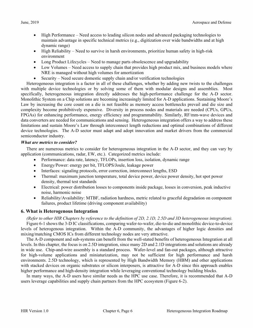
Chiplet Standardized Interfaces
Figure 7-18. Intel Advanced Interface Bus (AIB) specification enables modular design14
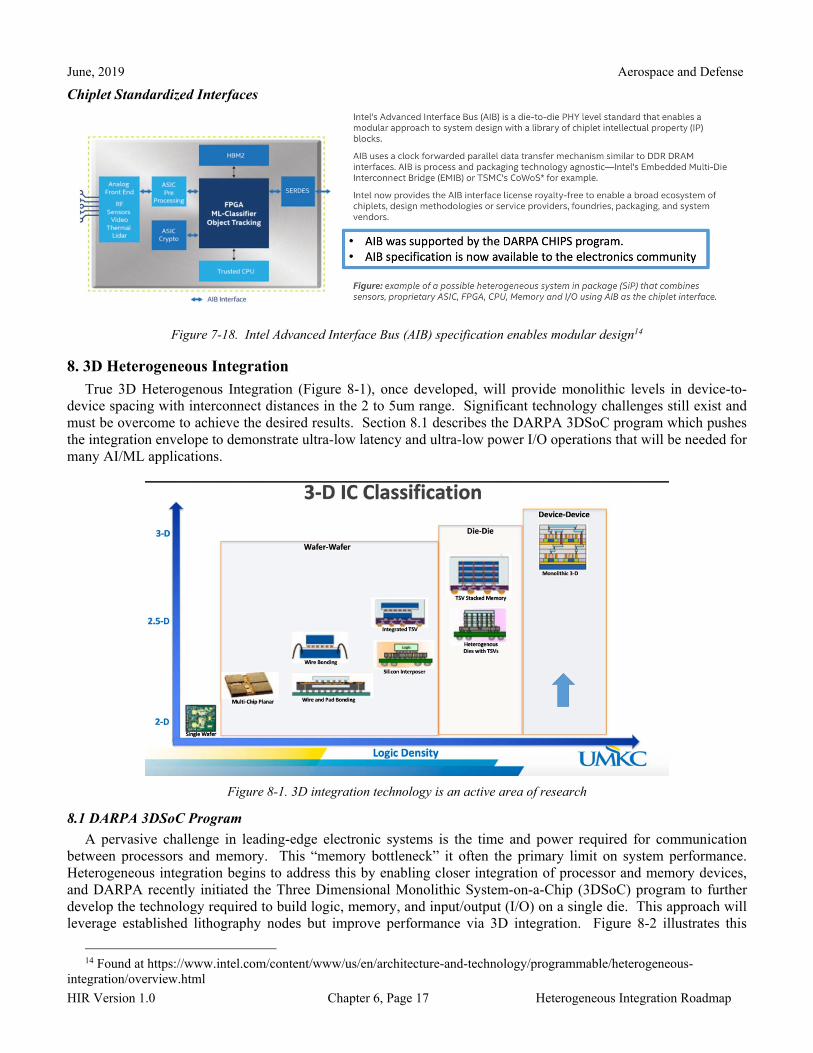
8. 3D Heterogeneous Integration
True 3D Heterogenous Integration (Figure 8-1), once developed, will provide monolithic levels in device-to-device spacing with interconnect distances in the 2 to 5um range. Significant technology challenges still exist and must be overcome to achieve the desired results. Section 8.1 describes the DARPA 3DSoC program which pushes the integration envelope to demonstrate ultra-low latency and ultra-low power I/O operations that will be needed for many AI/ML applications.
Figure 8-1. 3D integration technology is an active area of research
8.1 DARPA 3DSoC Program
A pervasive challenge in leading-edge electronic systems is the time and power required for communication between processors and memory. This “memory bottleneck” it often the primary limit on system performance. Heterogeneous integration begins to address this by enabling closer integration of processor and memory devices, and DARPA recently initiated the Three Dimensional Monolithic System-on-a-Chip (3DSoC) program to further develop the technology required to build logic, memory, and input/output (I/O) on a single die. This approach will leverage established lithography nodes but improve performance via 3D integration. Figure 8-2 illustrates this
14 Found at https://www.intel.com/content/www/us/en/architecture-and-technology/programmable/heterogeneous-
integration/overview.html

June, 2019 Aerospace and Defense
HIR Version 1.0 Chapter 6, Page 18 Heterogeneous Integration Roadmap
approach where progress is made via 3D integration rather than further advances following Moore’s Law. Figure 8-3 shows more detail of the envisioned 3D integration of novel device types.
Figure 8.2 The DARPA 3DSoC program attacks the end of Moore’s Law by the reduction of interconnect distances through vertical integration
Figure 8-3. DARPA 3DSoC will demonstrate the tight integration of CNFET logic with ReRAM to have similar performance of FinFETs while using 90nm fabrication line

June, 2019 Aerospace and Defense
HIR Version 1.0 Chapter 6, Page 19 Heterogeneous Integration Roadmap
9. Outlook for Next 5 to 10 Years
9.1 DARPA CHIPS 2.0 (3 to 5 Years)
DARPA CHIPS is now seeking to foster a design and manufacturing chiplet eco-system for DoD users. Figures 9-1 and 9-2 show the requirements for silicon interposers, based on findings during Phase 1 of the CHIPS program. As progress is made, the A-D Chapter will be updated with the outcomes.
Figure 9-1. CHIPS wishlist for chiplet ecosystem
Figure 9-2. timeline for CHIPS 2.0 vision

June, 2019 Aerospace and Defense
HIR Version 1.0 Chapter 6, Page 20 Heterogeneous Integration Roadmap
9.2 Modular Single-Wafer Fabrication (5 to 10 Years)
Recent research in Japan is developing a concept called “minimal fab” which may offer a future solution for enabling high-mix, low-volume production of semiconductors, MEMS, and other microdevices.
TOKYO Semiconductor start-up NEITAS has succeeded in creating semiconductor components in 20 hours – just a fraction of the time normally required – using a "minimal fab," a system that can produce even a single wafer with low capital spending. The breakthrough was confirmed jointly with Toyohashi University of Technology in Toyohashi, Aichi Prefecture. The company plans to set up a contract fabrication plant in Okinawa by the end of the year with the aim of achieving 10 billion yen ($88.4 million) in sales by 2020.15
The minimal fab was born at the National Institute of Advanced Industrial Science and Technology (AIST) in Tsukuba, Ibaraki Prefecture. It can manufacture semiconductors using small wafers just 12.5mm, or 0.5 inch, in diameter.
Minimal fabs hold down costs. With existing fabrication systems, the circuit negatives known as masks that form circuits on wafers are expensive. But they are unnecessary in a minimal fab. Circuits are created by using some 1 million small mirrors. Clean rooms are also unnecessary because the processing is performed in enclosed spaces within the equipment.
Masks are not needed. As a result, the direct-exposure system has the challenge of reducing circuit linewidths. Using a maskless technology developed at Toyohashi University, the equipment is capable of defining 0.8 micron dimension. Although this is quite coarse for CMOS FEOL, this is the right ballpark for BEOL linewidths, so the most advanced lithography tools are not needed.
Figure 9-3. Minimal modular wafer fabrication technology
At "SEMICON Japan 2017"16, Minimal Fab exhibited their equipment that houses self-contained processing
capability for wafer cleaning, and exposure for wafers as small as 0.5 inch. A minimal shuttle container is used to move the wafer between processing machines. This type of equipment is suitable for small-lot production and is useful for research and development with drastically reduced capital costs. Minimal Fab is working with Disco, Ishii
15 https://asia.nikkei.com/Business/Biotechnology/Minimal-fab-tech-promises-faster-cheaper-chip-production 16 https://www.ewarrant-
sec.jp/article/%E3%81%8B%E3%81%AE%E3%81%86%E3%81%A1%E3%81%82%E3%82%84%E3%81%93%E3%81%AE%E3%80%8Csemicon-japan-2017%E3%80%8D%E3%83%AC%E3%83%9D%E3%83%BC%E3%83%88/

June, 2019 Aerospace and Defense
HIR Version 1.0 Chapter 6, Page 21 Heterogeneous Integration Roadmap
Craft Research Institute, Apic Yamada and others to foster a minimal-equipment ecosystem. Yokogawa Solution Service17 will act as a contact point to order and sell various equipment from different manufacturers.18
Figure 9-4. Minimal Fab’s approach to low-volume semiconductor fabrication without clean-room
10. DARPA Electronics Resurgence Initiative (ERI)
In 2018, DARPA’s Microsystem Technology Office (MTO) launched the Electronics Resurgence Initiative (ERI)19
Today’s critical Department of Defense (DOD) systems and platforms rely on advanced electronics to address national security objectives.
To help tackle obstacles facing a half-century of electronics advancement, DARPA launched the Electronics Resurgence Initiative (ERI) – a five-year, upwards of US$1.5 billion investment in the future of domestic electronic systems.
Figure 10-1 shows the ERI Materials pillar that supports DARPA CHIPS and 3DSOC programs. Both programs are expected to continue over the next 2-3 years. The PIPES program which will launch in 2019 will support the heterogenous integration of Photonic IC devices with CMOS.
17 https://www.yokogawa.com/yjp/biz/semi/minimal-fab.htm?nid=left 18 https://eetimes.jp/ee/articles/1712/18/news033.html 19 https://www.darpa.mil/news-events/electronics-resurgence-initiative-summit

June, 2019 Aerospace and Defense
HIR Version 1.0 Chapter 6, Page 22 Heterogeneous Integration Roadmap
Figure 10-1. DARPA Electronics Resurgence Initiative
11. Supply Chain
12.1 International Supply Chain
The NDIA Trusted Microelectronics Team 1 Report asks: “Increasing Supply Chain Complexity: Commercially available capability (complex global infrastructure involved in SOTA designs; Fabs, IP, Packaging, Testing, etc.) is rapidly increasing, accomplished through a complex disaggregated supply chain that is fragile and subject to compromise. How can it be safely utilized?”20
Figure 11-1. IC manufacturing in a globalized independent supply chain21
20 http://www.ndia.org/-/media/sites/ndia/divisions/working-groups/tmjwg-documents/ndia-tm-jwg-team-1-white-paper-
finalv3.ashx?la=en 21 Found at http://www.businessdefense.gov/Portals/51/Documents/Resources/2016%20AIC%20RTC%2006-27-17%20-
%20Public%20Release.pdf?ver=2017-06-30-144825-160

June, 2019 Aerospace and Defense
HIR Version 1.0 Chapter 6, Page 23 Heterogeneous Integration Roadmap
Foundries concentrated in Asia Chinese players growing Increasingly consolidated among leaders
Access must also be reiterated here as a critical challenge and concern. While access to trusted components is already understood as a core concern, simple access to the parts needed from the larger global electronics industry base is an even larger concern. Figure 11-2 describes this concern, and emphasizes the need to take seriously the larger strategic issue of continued assured access to components for our current and future DoD systems.
This is a major concern as the globalization and consolidation of microelectronics companies is driven by demand in the commercial markets rather than by the needs within the Defense markets. Achieving continued assured access to advanced microelectronics components is imperative for the DoD to maintain the strongest Defense and Intelligence communities in the world. Without a coherent national strategy, the US government risks losing its ability to protect its key systems and the US microelectronics industry will lose its leadership role in this critical market.
Figure 11-2. Changing foundry landscape
Figure 11-3. Nearly all foundry growth in 2018 driven by customers in China

June, 2019 Aerospace and Defense
HIR Version 1.0 Chapter 6, Page 24 Heterogeneous Integration Roadmap
Figure 11-4. OSAT companies ranking 2017 (millions of US$)22
13. HIR Aerospace-Defense TWG Team
Name Affiliation RoleTim Lee Boeing Co-chairJeff Demmin Booz Allen Hamilton Co-chairTom Kazior Raytheon MemberDan Blass Lockheed Martin Member
Edited by Paul Wesling 22 Found at https://anysilicon.com/osat-companies-ranking-2016-2017/