chapter 6 - microwave power tubeskmg/files/literature/power vacuum... · whitaker, jerry c....
TRANSCRIPT

Whitaker, Jerry C. “Chapter 6 – Microwave Power Tubes” Power Vacuum Tubes Handbook 2nd Edition.Ed. Jerry C. WhitakerBoca Raton: CRC Press LLC, 2000
© 1999 CRC Press LLC
Chapter
6Microwave Power Tubes
6.1 IntroductionMicrowave power tubes span a wide range of applications, operating at frequenciesfrom 300 MHz to 300 GHz with output powers from a few hundred watts to more than10 MW. Applications range from the familiar to the exotic. The following devices areincluded under the general description of microwave power tubes:
• Klystron, including the reflex and multicavity klystron
• Multistage depressed collector (MSDC) klystron
• Inductive output tube (IOT)
• Traveling wave tube (TWT)
• Crossed-field tube
• Coaxial magnetron
• Gyrotron
• Planar triode
• High-frequency tetrode
• Diacrode
This wide variety of microwave devices has been developed to meet a broad range ofapplications. Some common uses include:
• UHF-TV transmission
• Shipboard and ground-based radar
• Weapons guidance systems
• Electronic countermeasure (ECM) systems
• Satellite communications
• Tropospheric scatter communications
© 1999 CRC Press LLC

• Fusion research
As new applications are identified, improved devices are designed to meet theneeds. Microwave power tube manufacturers continue to push the limits of frequency,operating power, and efficiency. Microwave technology, therefore, is an evolving sci-ence. Figure 6.1 charts device type as a function of operating frequency and power out-put.
Two principal classes of microwave vacuum devices are in common use today:
• Linear-beam tubes
• Crossed-field tubes
Each class serves a specific range of applications. In addition to these primaryclasses, some power grid tubes also are used at microwave frequencies.
6.1.1 Linear-Beam Tubes
In a linear-beam tube, as the name implies, the electron beam and the circuit elementswith which it interacts are arranged linearly. The major classifications of linear-beamtubes are shown in Figure 6.2. In such a device, a voltage applied to an anode acceler-ates electrons drawn from a cathode, creating a beam of kinetic energy. Power supplypotential energy is converted to kinetic energy in the electron beam as it travels to-ward the microwave circuit. A portion of this kinetic energy is transferred to micro-wave energy as RF waves slow down the electrons. The remaining beam energy is ei-ther dissipated as heat or returned to the power supply at the collector. Because elec-trons will repel one another, there usually is an applied magnetic focusing field tomaintain the beam during the interaction process. The magnetic field is supplied ei-ther by a solenoid or permanent magnets. Figure 6.3 shows a simplified schematic ofa linear-beam tube.
6.1.2 Crossed-Field Tubes
The magnetron is the pioneering device of the family of crossed-field tubes. The fam-ily tree of this class of devices is shown in Figure 6.4. Although the physical appear-ance differs from that of linear-beam tubes, which are usually circular in format, themajor difference is in the interaction physics that requires a magnetic field at right an-gles to the applied electric field. Whereas the linear-beam tube sometimes requires amagnetic field to maintain the beam, the crossed-field tube always requires a mag-netic focusing field.
Figure 6.5 shows a cross section of the magnetron, including the magnetic field ap-plied perpendicular to the cathode-anode plane. The device is basically a diode with theanode composed of a plurality of resonant cavities. The interaction between the elec-trons emitted from the cathode and the crossed electric and magnetic fields produces aseries of space-charge spokes that travel around the anode-cathode space in a mannerthat transfers energy to the RF signal supported by the multicavity circuit. The mecha-nism is highly efficient.
© 1999 CRC Press LLC

Figure 6.1 Microwave power tube type as a function of frequency and output power.
© 1999 C
RC
Press LL
C

Figure 6.2 Types of linear-beam microwave tubes.
Figure 6.3 Schematic diagram of a linear-beam tube.
© 1999 CRC Press LLC

Crossed-Field Amplifiers
Figure 6.6 shows the family tree of the crossed-field amplifier (CFA). The configura-tion of a typical present-day distributed emission amplifier is similar to that of themagnetron except that the device has an input for the introduction of RF energy intothe circuit. Current is obtained primarily by secondary emission from the negative
Figure 6.4 Types of crossed-field microwave tubes.
Figure 6.5 Magnetron electron path looking down into the cavity with the magnetic fieldapplied.
© 1999 CRC Press LLC

electrode that serves as a cathode throughout all or most of the interaction space. Theearliest versions of this tube type were called amplitrons.
The CFA is deployed in radar systems operating from UHF to the Ku-band, and atpower levels up to several megawatts. In general, bandwidth ranges from a few percentto as much as 25 percent of the center frequency.
6.2 Grid Vacuum TubesThe physical construction of a vacuum tube causes the output power and availablegain to decrease with increasing frequency. The principal limitations faced bygrid-based devices include the following:
• Physical size. Ideally, the RF voltages between electrodes should be uniform, butthis condition cannot be realized unless the major electrode dimensions are sig-nificantly less than 1/4 wavelength at the operating frequency. This restrictionpresents no problems at VHF, but as the operating frequency increases into themicrowave range, severe restrictions are placed on the physical size of individualtube elements.
• Electron transit time. Interelectrode spacing, principally between the grid and thecathode, must be scaled inversely with frequency to avoid problems associatedwith electron transit time. Possible adverse conditions include: 1) excessive load-ing of the drive source, 2) reduction in power gain, 3) back-heating of the cathodeas a result of electron bombardment, and 4) reduced conversion efficiency.
Figure 6.6 Family tree of the distributed emission crossed-field amplifier (CFA).
© 1999 CRC Press LLC

• Voltage standoff. High-power tubes operate at high voltages. This presents sig-nificant problems for microwave vacuum tubes. For example, at 1 GHz thegrid-cathode spacing must not exceed a few mils. This places restrictions on theoperating voltages that may be applied to the individual elements.
• Circulating currents. Substantial RF currents may develop as a result of the inher-ent interelectrode capacitances and stray inductances/capacitances of the device.Significant heating of the grid, connecting leads, and vacuum seals may result.
• Heat dissipation. Because the elements of a microwave grid tube must be keptsmall, power dissipation is limited.
Still, a number of grid-based vacuum tubes find applications at high frequencies. Forexample, planar triodes are available that operate at several gigahertz, with outputpowers of 1 to 2 kW in pulsed service. Efficiency (again for pulsed applications)ranges from 30 to 60 percent, depending on the frequency.
6.2.1 Planar Triode
A cross-sectional diagram of a planar triode is shown in Figure 6.7. The envelope ismade of ceramic, with metal members penetrating the ceramic to provide for connec-tion points. The metal members are shaped either as disks or as disks with cylindricalprojections.
The cathode is typically oxide-coated and indirectly heated. The key design objec-tive for a cathode is high emission density and long tube life. Low-temperature emittersare preferred because high cathode temperatures typically result in more evaporationand shorter life.
The grid of the planar triode is perhaps the greatest design challenge for tube manu-facturers. Close spacing of small-sized elements is needed, at tight tolerances. Goodthermal stability also is required, because the grid is subjected to heating from currentsin the element itself, plus heating from the cathode and bombardment of electrons fromthe cathode.
The anode, usually made of copper, conducts the heat of electron bombardment toan external heat sink. Most planar triodes are air-cooled.
Planar triodes designed for operation at 1 GHz and above are used in a variety of cir-cuits. The grounded-grid configuration is most common. The plate resonant circuit iscavity-based, using waveguide, coaxial line, or stripline. Electrically, the operation ofthe planar triode is much more complicated at microwave frequencies than at low fre-quencies. Figure 6.8a compares the elements at work for a grounded-grid amplifier op-erating at low frequencies and Figure 6.8b compares the situation at microwave fre-quencies. The equivalent circuit is made more complex by:
• Stray inductance and capacitance of the tube elements
• Effects of the tube contact rings and socket elements
• Distributed reactance of cavity resonators and the device itself
© 1999 CRC Press LLC

• Electron transit-time effects, which result in resistive loading and phase shifts
Reasonable gains of 5 to 10 dB may be achieved with a planar triode. Increased gainis available by cascading stages. Interstage coupling may consist of waveguide or coax-ial-line elements. Tuning is accomplished by varying the cavity inductance or capaci-tance. Additional bandwidth is possible by stagger tuning of cascaded stages.
6.2.2 High-Power UHF Tetrode
New advancements in vacuum tube technology have permitted the construction ofhigh-power UHF transmitters based on tetrodes. Such devices are attractive becausethey inherently operate in a relatively efficient class AB mode. UHF tetrodes operat-ing at high power levels provide essentially the same specifications, gain, and effi-ciency as tubes operating at lower powers. The anode power supply is much lower involtage than the collector potential of a klystron- or IOT-based system (8 kV is com-mon). Also, the tetrode does not require a focusing magnet system.
Figure 6.7 Cross section of a 7289 planar triode.
© 1999 CRC Press LLC

Efficient removal of heat is the key to making a tetrode practical at high power lev-els. Such devices typically use water or vapor-phase cooling. Air cooling at such levelsis impractical because of the fin size that would be required. Also, the blower for thetube would have to be quite large, reducing the overall transmitter ac-to-RF efficiency.
Another drawback inherent in tetrode operation is that the output circuit of the de-vice appears electrically in series with the input circuit and the load [1]. The parasiticreactance of the tube elements, therefore, is a part of the input and output tuned circuits.It follows, then, that any change in the operating parameters of the tube as it ages can af-fect tuning. More importantly, the series nature of the tetrode places stringent limita-tions on internal element spacings and the physical size of those elements in order tominimize the electron transit time through the tube vacuum space. It is also fair to pointout, however, the tetrode’s input-to-output circuit characteristic has at least one advan-tage: power delivered to the input passes through the tube and contributes to the totalpower output of the transmitter. Because tetrodes typically exhibit low gain compared
Figure 6.8 Grounded-grid equivalent circuits: (a) low-frequency operation, (b) micro-wave-frequency operation. The cathode-heating and grid-bias circuits are not shown.
(a)
(b)
© 1999 CRC Press LLC

to a klystron-based device, significant power can be required at the input circuit. Thepass-through effect, therefore, contributes to the overall operating efficiency of thetransmitter.
The expected lifetime of a tetrode in UHF service is usually shorter than a klystronof the same power level. Typical lifetimes of 8,000 to 15,000 hours have been reported.Intensive work, however, has led to products that offer higher output powers and ex-tended operating lifetime, while retaining the benefits inherent in tetrode devices.
6.2.3 Diacrode
The Diacrode (Thomson) is a promising adaptation of the high-power UHF tetrode.The operating principle of the Diacrode is basically the same as that of the tetrode. Theanode current is modulated by an RF drive voltage applied between the cathode and thepower grid. The main difference is in the position of the active zones of the tube in theresonant coaxial circuits, resulting in improved reactive current distribution in the elec-trodes of the device.
Figure 6.9 compares the conventional tetrode with the Diacrode. The Diacrode in-cludes an electrical extension of the output circuit structure to an external cavity [2].The small dc-blocked cavity rests on top of the tube, as illustrated in Figure 6.10.
The cavity is a quarter-wave transmission line, as measured from the top of the cav-ity to the vertical center of the tube. The cavity is short-circuited at the top, reflecting anopen circuit (current minimum) at the vertical center of the tube and a current maxi-mum at the base of the tube, like the conventional tetrode, and a second current maxi-mum above the tube at the cavity short-circuit.
Figure 6.9 Cutaway view of the tetrode (left) and the Diacrode (right). Note that the RFcurrent peaks above and below the Diacrode center while on the tetrode there is onlyone peak at the bottom. (After [2].)
© 1999 CRC Press LLC

With two current maximums, the RF power capability of the Diacrode is double thatof the equivalent tetrode, while the element voltages remain the same. All other proper-ties and aspects of the Diacrode are basically identical to the TH563 high-power UHFtetrode (Thomson), upon which the Diacrode is patterned.
Some of the benefits of such a device, in addition to the robust power output avail-able, is the low high-voltage requirements (low relative to a klystron/IOT-based system,that is), small size, and simple replacement procedures. On the downside, there is littleinstalled service lifetime data at this writing because the Diacrode is relatively new tothe market.
6.3 KlystronThe klystron is a linear-beam device that overcomes the transit-time limitations of agrid-controlled tube by accelerating an electron stream to a high velocity before it ismodulated. Modulation is accomplished by varying the velocity of the beam, whichcauses the drifting of electrons into bunches to produce RF space current. One ormore cavities reinforce this action at the operating frequency. The output cavity actsas a transformer to couple the high-impedance beam to a low-impedance transmissionline. The frequency response of a klystron is limited by the impedance-bandwidthproduct of the cavities, but may be extended through stagger tuning or the use of mul-tiple-resonance filter-type cavities.
The klystron is one of the primary means of generating high power at UHF andabove. Output powers for multicavity devices range from a few thousand watts to 10
Figure 6.10 The elements of the Diacrode, including the upper cavity. Double current,and consequently, double power, is achieved with the device because of the currentpeaks at the top and bottom of the tube, as shown. (After [2].)
© 1999 CRC Press LLC

MW or more. The klystron provides high gain and requires little external support cir-cuitry. Mechanically, the klystron is relatively simple. It offers long life and requiresminimal routine maintenance.
6.3.1 Reflex Klystron
The reflex klystron uses a single-cavity resonator to modulate the RF beam and ex-tract energy from it. The construction of a reflex klystron is shown in Figure 6.11. Inits basic form, the tube consists of the following elements:
• A cathode
• Focusing electrode at cathode potential
• Coaxial line or reentrant-type cavity resonator, which also serves as an anode
• Repeller or reflector electrode, which is operated at a moderately negative poten-tial with respect to the cathode
The cathode is so shaped that, in relation to the focusing electrode and anode, an elec-tron beam is formed that passes through a gap in the resonator, as shown in the figure,and travels toward the repeller. Because the repeller has a negative potential with re-spect to the cathode, it turns the electrons back toward the anode, where they passthrough the anode gap a second time. By varying the applied voltage on the reflector
Figure 6.11 Schematic representation of a reflex klystron.
© 1999 CRC Press LLC
electrode, phasing of the beam can be varied to produce the desired oscillating modeand to control the frequency of oscillation.
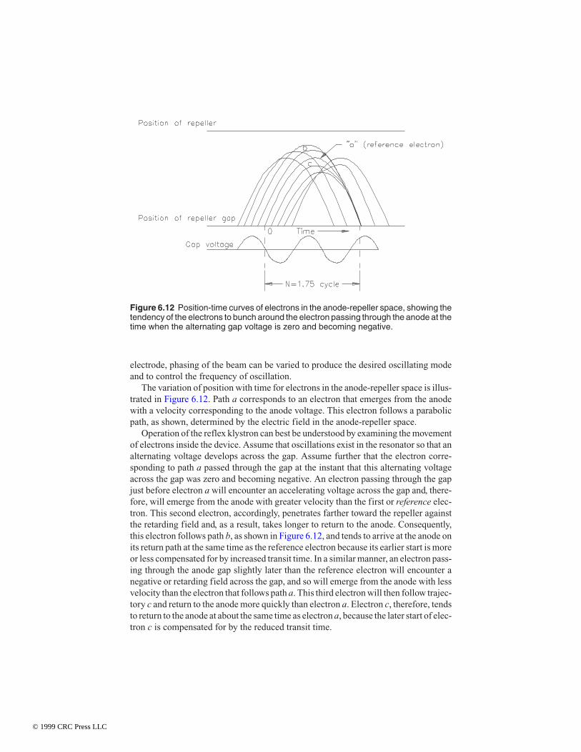
The variation of position with time for electrons in the anode-repeller space is illus-trated in Figure 6.12. Path a corresponds to an electron that emerges from the anodewith a velocity corresponding to the anode voltage. This electron follows a parabolicpath, as shown, determined by the electric field in the anode-repeller space.
Operation of the reflex klystron can best be understood by examining the movementof electrons inside the device. Assume that oscillations exist in the resonator so that analternating voltage develops across the gap. Assume further that the electron corre-sponding to path a passed through the gap at the instant that this alternating voltageacross the gap was zero and becoming negative. An electron passing through the gapjust before electron a will encounter an accelerating voltage across the gap and, there-fore, will emerge from the anode with greater velocity than the first or reference elec-tron. This second electron, accordingly, penetrates farther toward the repeller againstthe retarding field and, as a result, takes longer to return to the anode. Consequently,this electron follows path b, as shown in Figure 6.12, and tends to arrive at the anode onits return path at the same time as the reference electron because its earlier start is moreor less compensated for by increased transit time. In a similar manner, an electron pass-ing through the anode gap slightly later than the reference electron will encounter anegative or retarding field across the gap, and so will emerge from the anode with lessvelocity than the electron that follows path a. This third electron will then follow trajec-tory c and return to the anode more quickly than electron a. Electron c, therefore, tendsto return to the anode at about the same time as electron a, because the later start of elec-tron c is compensated for by the reduced transit time.
Figure 6.12 Position-time curves of electrons in the anode-repeller space, showing thetendency of the electrons to bunch around the electron passing through the anode at thetime when the alternating gap voltage is zero and becoming negative.
© 1999 CRC Press LLC

This variation with time of the velocity of electrons emerging from the anode istermed velocity modulation. The effect of this phenomenon can be seen in Figure 6.12to cause a bunching of electrons about the electron that passed through the gap when theresonator voltage was zero and becoming negative. This bunching causes the electronsthat are returned toward the anode by the repeller to pass through the anode gap inbursts or pulses, one each cycle. When these pulses pass through the gap at such a timethat the electrons in the pulse are slowed as a result of the alternating voltage existingacross the gap at the instant of their return passage, energy will be delivered to the oscil-lations in the resonator, thereby assisting in maintaining the oscillations. This conditioncorresponds to a transit time N from the resonator toward the repeller and back to theresonator of approximately:
N n= + 34 (6.1)
Where:n = an integer (including zero)
The transit time in the anode-repeller space in any particular case depends upon thefollowing:
• The anode voltage
• Repeller voltage
• Geometry of the anode-repeller space
The extent of the bunching action that takes place when the transit time of the refer-ence electron has the correct value for sustaining oscillations is determined by the fol-lowing:
• The amplitude of the alternating voltage across the resonator gap in relation to theanode and repeller voltage
• The geometry of the repeller space
The reflex klystron typically includes a grid to concentrate the electric field so that itmay efficiently couple to the electron beam. Such a device is illustrated in Figure 6.13.
The reflex klystron may be used as a local oscillator, low-power FM transmitter, ortest signal source. Reflex tubes are used primarily from 4 to 40 GHz. Power outputs of 1W or less are common.
The reflex tube is the only klystron in which beam feedback is used to produce out-put energy. In klystrons with more than one cavity, the electron beam passes througheach cavity in succession.
6.3.2 The Two-Cavity Klystron
The two-cavity klystron operates on the same bunching principle as the reflex kly-stron, but incorporates two cavities connected by a drift tube. Figure 6.14 shows across section of a classic device. The heater/cathode element (shown as A in the fig-
© 1999 CRC Press LLC

ure) produces an electron beam in conjunction with a focusing electrode. The routetaken by the electrons is as follows:
• The beam passes through grid elements D in the side of a reentrant cavity resona-tor (the buncher).
• The beam then passes through the drift tube, which is at the same electrical poten-tial as the buncher.
• Finally, the beam enters a second resonator termed the collector, which is pro-vided with a grid E.
The cathode and its associated focusing electrode are maintained at a high negativepotential with respect to the remaining part of the structure, all of which is at the samedc potential. The entire arrangement illustrated in the figure is enclosed in a vacuum.
The operational principles of the two-cavity klystron are similar in nature to those ofthe reflex klystron. Assume, first, that oscillations exist in the buncher so that an alter-nating voltage is present across the gap D. When this voltage is zero but just becomingpositive, an electron passing through the buncher travels through the grids D, down thedrift tube, and into the collector resonator with unchanged velocity. However, an elec-tron that passes through the buncher slightly later receives acceleration while passingthrough, because of the positive alternating field that it encounters between grids D,and enters the drift tube with increased velocity. This later electron, therefore, tends toovertake the earlier electron. Similarly, an electron that arrives at the buncher slightly
Figure 6.13 Schematic cross section of a reflex klystron oscillator.
© 1999 CRC Press LLC

earlier than the first (reference electron) encounters a field between grids D that op-poses its motion. Hence, this early electron enters the drift tube with reduced velocityand tends to drop back and be overtaken by the reference electron.
As a result of these actions, the electrons bunch together as they travel down the drifttube. This effect is more pronounced at certain distances from the buncher. If the col-lector is located at a distance where the bunching is pronounced, the electrons enter theelement in pulses, one pulse per cycle.
With proper adjustment, the amount of power required to produce the bunching ef-fect is relatively small compared with the amount of energy delivered by the electronbeam to the collector. As a result, the klystron operates as an amplifying device.
The Two-Cavity Klystron Oscillator
The two-cavity klystron oscillator is designed for applications requiring moderatepower (up to 100 W), stable frequency output, and low sideband noise. The device hasa coupling iris on the wall between the two cavities. The tube can be frequency-modu-lated by varying the cathode voltage about the center of the oscillating mode. Al-though it is more efficient and powerful than the reflex klystron, the two-cavity kly-
Figure 6.14 Cross section of a classic two-cavity klystron oscillator.
© 1999 CRC Press LLC

stron requires more modulator power. The two-cavity klystron typically is used inDoppler radar systems.
The Two-Cavity Klystron Amplifier
Similar in design to the two-cavity oscillator, the two-cavity klystron amplifier pro-vides limited power output (10 W or less) and moderate gain (about 10 dB). A drivingsignal is coupled into the input cavity, which produces velocity modulation of thebeam. After the drift space, the density-modulated beam induces current in the outputresonator. Electrostatic focusing of the beam is common.
The two-cavity klystron finds only limited applications because of its restrictions onoutput power and gain. For many applications, solid-state amplifiers are a better choice.
6.3.3 The Multicavity Klystron
The multicavity klystron is an important device for amplifying signals to high powerlevels at microwave frequencies [3]. Each cavity tuned to the operating frequencyadds about 20 dB gain to the 10 dB gain offered by the basic two-cavity klystron am-plifier. Overall gains of 60 dB are practical. Cavities may be tuned to either side ofresonance to broaden the operating bandwidth of the device. Klystrons with up toeight cavities have been produced. Operating power for continuous wave klystronsranges up to 1 MW per device, and as much as 50 MW per device for pulsed applica-tions.
The primary physical advantage of the klystron over a grid-based power tube is thatthe cathode-to-collector structure is virtually independent of transit-time effects.Therefore, the cathode can be made large and the electron beam density kept low.
The operating frequency of a klystron may be fixed—determined by the mechanicalcharacteristics of the tube and its cavities—or tunable. Cavities are tuned mechanicallyusing one of several methods, depending on the operating power and frequency. Tuningis accomplished by changing the physical dimensions of the cavities using one or moreof the following techniques:
• Cavity wall deformation, in which one wall of the cavity consists of a thin dia-phragm that is moved in and out by a tuning mechanism. About 3 percent fre-quency shift may be accomplished using this method, which varies the induc-tance of the cavity.
• Movable cavity wall, in which one wall of the cavity is moved in or out by a tuningmechanism. About 10 percent frequency shift is possible with this approach,which varies the inductance of the cavity.
• Paddle element, in which an element inside the cavity moves perpendicularly tothe beam and adds capacitance across the interaction gap. A tuning range of about25 percent is provided by this approach.
• Combined inductive-capacitive tuning, which uses a combination of the previousmethods. Tuning variations of 35 percent are possible.
© 1999 CRC Press LLC

Each of these tuning methods may be used whether the cavity is inside or outside thevacuum envelope of the tube. Generally speaking, however, tubes that use externalcavities provide more adjustment range, usually on the order of 35 percent. Band-width may be increased by stagger tuning of the cavities, at the expense of gain.
High conversion efficiency requires the formation of electron bunches, which oc-cupy a small region in velocity space, and the formation of interbunch regions with lowelectron density. The latter is particularly important because these electrons are phasedto be accelerated into the collector at the expense of the RF field. Studies show that theenergy loss as a result of an electron accelerated into the collector may exceed the en-ergy delivered to the field by an equal but properly phased electron. Therein lies a key inimproving the efficiency of the klystron: Recover a portion of this wasted energy.
Klystrons are cooled by air or liquid for powers up to 5 kW. Tubes operating in ex-cess of 5 kW are usually water- or vapor-cooled.
Operating Principles
A high-velocity electron beam emitted from the cathode passes through the anode andinto the RF interaction region, as shown in Figure 6.15 [3]. An external magnetic fieldis employed to prevent the beam from spreading as it passes through the tube. At theother end of the device, the electron beam impinges on the collector electrode, whichdissipates the beam energy and returns the electron current to the beam power supply.
Figure 6.15 Principal elements of a klystron.
© 1999 CRC Press LLC

The RF interaction region, where amplification occurs, contains resonant cavitiesand field-free drift spaces. The first resonant cavity encountered by an electron in thebeam (the input cavity) is excited by the microwave signal to be amplified, and an alter-nating voltage of the signal frequency is developed across the gap. This action can bebest explained by drawing an analogy between a resonant cavity and a conventionalparallel resonant LC circuit (see Figure 6.16). The cavity gap corresponds to the capaci-tor, and the volume of the cavity to the inductor. If the cavity is of the correct physicaldimensions, it will resonate at the desired microwave frequency. At resonance, oppositesides of the gap become alternately positive and negative at a frequency equal to the mi-crowave input signal frequency.
An electron passing through the gap when the voltage across the gap is zero contin-ues with unchanged velocity along the drift tube toward the next cavity gap; this elec-tron is the reference electron. An electron passing through the same gap slightly later isaccelerated by the positive field at the gap. This electron speeds up and tends to over-take the reference electron ahead of it in the drift tube. However, an electron that passesthrough the gap slightly ahead of the reference electron encounters a negative field andis slowed down. This electron tends to fall back toward the following reference elec-tron. As a result of passing the alternating field of the input-cavity gap, the electronsgradually bunch together as they travel down the drift tube, as illustrated in Figure 6.17.Because electrons approach the input-cavity gap with equal velocities and emerge withdifferent velocities, which are a function of the microwave signal, the electron beam issaid to be velocity-modulated. As the electrons travel down the drift tube, bunching de-velops, and the density of electrons passing a given point varies cyclically with time.This bunching is identical in nature to the action in a two-cavity klystron, discussed inSection 6.3.2.
The modulation component of the beam current induces current in each of the fol-lowing cavities. Because each cavity is tuned near resonance, the resulting increase infield at each gap produces successively better-defined electron bunches and, conse-quently, amplification of the input signal. The RF energy produced in this interactionwith the beam is extracted from the beam and fed into a coaxial or waveguide transmis-sion line by means of a coupling loop in the output cavity. The dc beam input power notconverted to RF energy is dissipated in the collector.
Figure 6.16 Klystron cavity: (a) physical arrangement, (b) equivalent circuit.
(a) (b)
© 1999 CRC Press LLC

Emission
The electron gun section of a klystron, shown in Figure 6.18, consists of the followingelements [3]:
• A heater
• An emitter
• A beam-forming focusing electrode
• A modulating anode
When the emitter temperature is raised to the proper value by the heater, electrons arereleased from the emitter surface. The electrons are accelerated toward the modulat-ing anode, which is at a positive potential with respect to the emitter. As the electronstravel between the emitter and the modulating anode, they are formed into a beam bythe lens action of the focusing electrode and modulating anode. Figure 6.19 showshow this lens is formed.
All cathodes have a specific optimum range of operating temperature. The tempera-ture of the cathode must be sufficiently high to prevent variations in heater power fromaffecting the electron emission current (beam current) in the klystron. However, thetemperature of the emitting surface must not be higher than necessary because exces-sive temperature can shorten emission life. Figure 6.20 shows beam current (emissioncurrent) as a function of the emitter temperature, which varies directly with heaterpower. When the heater voltage (Ef1) is too low, the emitter will not be hot enough to
Figure 6.17 Bunching effect of a multicavity klystron.
© 1999 CRC Press LLC

produce the desired beam current. In addition, even small variations in heater voltagewill change the beam current significantly. With the proper heater voltage (Ef2), con-stant beam current will be maintained even with minor variations in heater voltage. Thesame is true for a higher heater voltage value (Ef3), but in this case the emitter tempera-ture is greater than that needed for the desired beam current. Reduced tube life will re-
Figure 6.18 Diode section of a klystron electron gun.
Figure 6.19 Beam forming in the diode section of a klystron electron gun.
© 1999 CRC Press LLC

sult. The correct value of heater voltage and/or heater current is included in the datashipped with each klystron.
Modulating Anode
Because the modulating anode is electrically isolated from both the cathode and kly-stron body (the RF structure, between polepieces) the voltage applied to it provides aconvenient means for controlling beam current independently of the beam voltage ap-plied between the cathode and body, as shown in Figure 6.21. When the cathode is op-erated in the space-charge-limited region, Ef2 and Ef3 of Figure 6.20, the emission cur-rent will be a specific function of the applied voltage:
I k Eb = 32 (6.2)
Where:Ib = beam current in ampsE = beam potential in volts
The constant k is a function of the geometry of the cathode-anode structure, and istermed perveance. Because the modulating anode is physically positioned betweenthe RF structure (body) and the cathode, even if the full beam voltage is maintainedbetween cathode and body, the actual beam current into the tube may be reduced atwill by biasing the modulating anode to any voltage between cathode and body. Fig-ure 6.22 shows the relationship between beam current and voltage described in theprevious equation.
Figure 6.20 Klystron beam-current variation as a function of emitter temperature.
© 1999 CRC Press LLC
Magnetic Field
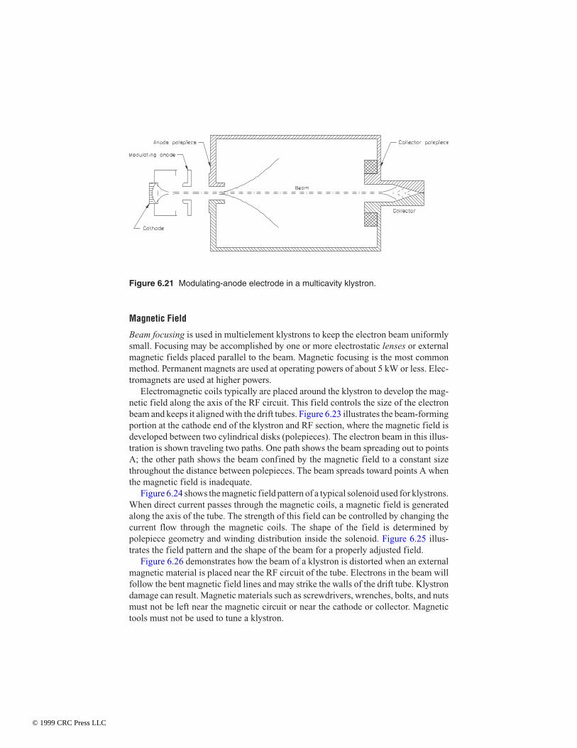
Beam focusing is used in multielement klystrons to keep the electron beam uniformlysmall. Focusing may be accomplished by one or more electrostatic lenses or externalmagnetic fields placed parallel to the beam. Magnetic focusing is the most commonmethod. Permanent magnets are used at operating powers of about 5 kW or less. Elec-tromagnets are used at higher powers.
Electromagnetic coils typically are placed around the klystron to develop the mag-netic field along the axis of the RF circuit. This field controls the size of the electronbeam and keeps it aligned with the drift tubes. Figure 6.23 illustrates the beam-formingportion at the cathode end of the klystron and RF section, where the magnetic field isdeveloped between two cylindrical disks (polepieces). The electron beam in this illus-tration is shown traveling two paths. One path shows the beam spreading out to pointsA; the other path shows the beam confined by the magnetic field to a constant sizethroughout the distance between polepieces. The beam spreads toward points A whenthe magnetic field is inadequate.
Figure 6.24 shows the magnetic field pattern of a typical solenoid used for klystrons.When direct current passes through the magnetic coils, a magnetic field is generatedalong the axis of the tube. The strength of this field can be controlled by changing thecurrent flow through the magnetic coils. The shape of the field is determined bypolepiece geometry and winding distribution inside the solenoid. Figure 6.25 illus-trates the field pattern and the shape of the beam for a properly adjusted field.
Figure 6.26 demonstrates how the beam of a klystron is distorted when an externalmagnetic material is placed near the RF circuit of the tube. Electrons in the beam willfollow the bent magnetic field lines and may strike the walls of the drift tube. Klystrondamage can result. Magnetic materials such as screwdrivers, wrenches, bolts, and nutsmust not be left near the magnetic circuit or near the cathode or collector. Magnetictools must not be used to tune a klystron.
Figure 6.21 Modulating-anode electrode in a multicavity klystron.
© 1999 CRC Press LLC

Figure 6.23 The effect of a magnetic field on the electron beam of a klystron.
Figure 6.22 Beam-current variation as a function of modulating-anode voltage.
© 1999 CRC Press LLC

RF Structure
The RF structure of a klystron amplifier consists of tunable resonant circuits (cavi-ties) positioned along the axis of the electron beam. The electron beam travelingthrough the cavities provides the necessary coupling between each of the RF circuits.
The cavities of a klystron are high-frequency parallel resonant circuits constructedso that they provide an RF voltage across the capacitive component (gap), which inter-acts with the dc beam. Figure 6.27a illustrates the polarity near the drift-tube tips withina cavity excited by an alternating voltage of microwave signal frequency. Figure 6.27b
Figure 6.24 Field pattern of a klystron electromagnet.
Figure 6.25 Field pattern and beam shape in a properly adjusted magnetic field.
© 1999 CRC Press LLC
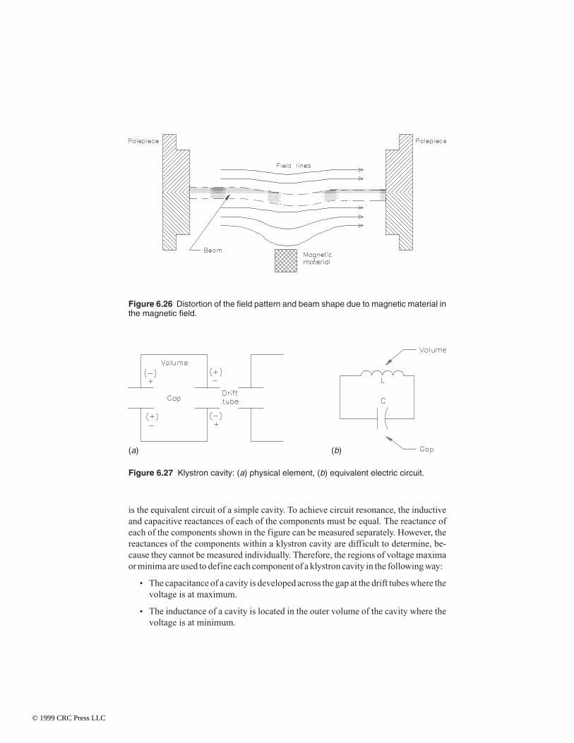
is the equivalent circuit of a simple cavity. To achieve circuit resonance, the inductiveand capacitive reactances of each of the components must be equal. The reactance ofeach of the components shown in the figure can be measured separately. However, thereactances of the components within a klystron cavity are difficult to determine, be-cause they cannot be measured individually. Therefore, the regions of voltage maximaor minima are used to define each component of a klystron cavity in the following way:
• The capacitance of a cavity is developed across the gap at the drift tubes where thevoltage is at maximum.
• The inductance of a cavity is located in the outer volume of the cavity where thevoltage is at minimum.
Figure 6.26 Distortion of the field pattern and beam shape due to magnetic material inthe magnetic field.
Figure 6.27 Klystron cavity: (a) physical element, (b) equivalent electric circuit.
(a) (b)
© 1999 CRC Press LLC
By defining each component of a cavity in these terms, it is easy to visualize changesin the volume as changes in inductance, and changes affecting the gap as changes incapacitance.
The resonant frequency of each cavity can be adjusted to the operating frequency ofthe RF generator. This can be accomplished in one of two ways:
• Change the inductance by changing the volume of the cavity.
• Change the capacitance of the drift-tube gaps.
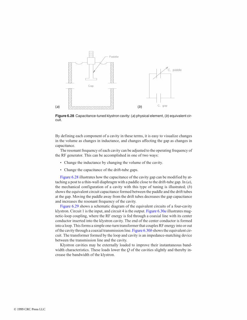
Figure 6.28 illustrates how the capacitance of the cavity gap can be modified by at-taching a post to a thin-wall diaphragm with a paddle close to the drift-tube gap. In (a),the mechanical configuration of a cavity with this type of tuning is illustrated; (b)shows the equivalent circuit capacitance formed between the paddle and the drift tubesat the gap. Moving the paddle away from the drift tubes decreases the gap capacitanceand increases the resonant frequency of the cavity.
Figure 6.29 shows a schematic diagram of the equivalent circuits of a four-cavityklystron. Circuit 1 is the input, and circuit 4 is the output. Figure 6.30a illustrates mag-netic-loop coupling, where the RF energy is fed through a coaxial line with its centerconductor inserted into the klystron cavity. The end of the center conductor is formedinto a loop. This forms a simple one-turn transformer that couples RF energy into or outof the cavity through a coaxial transmission line. Figure 6.30b shows the equivalent cir-cuit. The transformer formed by the loop and cavity is an impedance-matching devicebetween the transmission line and the cavity.
Klystron cavities may be externally loaded to improve their instantaneous band-width characteristics. These loads lower the Q of the cavities slightly and thereby in-crease the bandwidth of the klystron.
Figure 6.28 Capacitance-tuned klystron cavity: (a) physical element, (b) equivalent cir-cuit.
(a) (b)
© 1999 CRC Press LLC

Phased Electron Operation
By properly phasing the second-harmonic fields of a klystron, a favorable electrondensity distribution pattern can be established at the output gap. The result is the gen-eration of additional RF energy.
A phase-space diagram for a high-power klystron is shown in Figure 6.31. Thecurves represent a plot of the relative phase of the reference electrons as a function ofaxial distance along the tube. Electrons having negative slope have been decelerated.Electrons having positive slope have been accelerated with respect to a nonacceleratedelectron parallel to the axis. The diagram shows how the electrons are nicely grouped atthe output cavity gap while the interbunch regions are relatively free of electrons.
This interaction can be viewed another way, as shown in Figure 6.32, which plots thenormalized RF beam currents as a function of distance along the tube. The curves showthat the fundamental component of the plasma wave has a negative slope at the thirdgap. This normally would be a poor condition, but because of the drift of the interbunch
Figure 6.29 Schematic equivalent circuit of a four-cavity klystron.
Figure 6.30 Klystron loop coupling: (a) mechanical arrangement, (b) equivalent electriccircuit.
(a) (b)
© 1999 CRC Press LLC
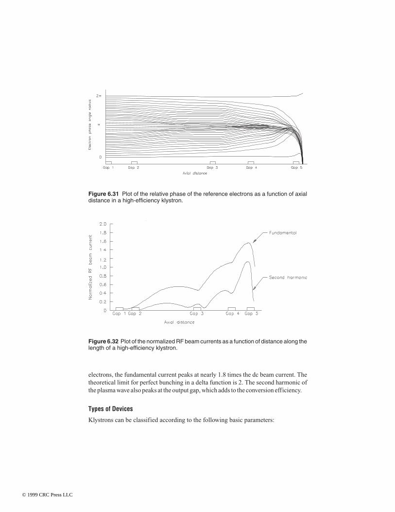
electrons, the fundamental current peaks at nearly 1.8 times the dc beam current. Thetheoretical limit for perfect bunching in a delta function is 2. The second harmonic ofthe plasma wave also peaks at the output gap, which adds to the conversion efficiency.
Types of Devices
Klystrons can be classified according to the following basic parameters:
Figure 6.31 Plot of the relative phase of the reference electrons as a function of axialdistance in a high-efficiency klystron.
Figure 6.32 Plot of the normalized RF beam currents as a function of distance along thelength of a high-efficiency klystron.
© 1999 CRC Press LLC

• Power operating level. Klystrons are available ranging from a few hundred wattsto more than 10 MW.
• Operating frequency. Klystrons typically are used over the frequency range of300 MHz to 40 GHz.
• Number of cavities. The number of resonant cavities may range from one to fiveor more. Furthermore, the cavities may be integral or external to the vacuum en-velope of the device.
The klystron is a true linear amplifier from zero signal level up to 2 to 3 dB belowsaturated output. Figure 6.33 shows a typical transfer characteristic for a klystron. RFmodulation is applied to the input drive signal. Amplitude modulation typically is lim-ited to the linear portion of the gain transfer characteristic (class A operation). The re-sult is low efficiency, because the beam power is always on. For applications requiringfrequency modulation, the drive power is set for saturated output.
Pulse modulation of the klystron may be obtained by applying a negative rectangularvoltage, instead of a dc voltage, to the cathode. The RF drive, set to a saturation value,usually is pulsed on for a slightly shorter time than the beam pulse.
Because of the high power levels typically used at UHF frequencies, device effi-ciency is a critical parameter. Klystrons usually are rated in terms of saturated effi-ciency, determined by dividing the saturated RF output power by the dc input power.
Saturated efficiency governs the maximum peak-of-sync efficiency available whenbeam-pulsing techniques are employed for UHF-TV service. Peak-of-sync efficiencyis the commonly used figure of merit (FOM) expression, defined as the peak-of-syncoutput power divided by the dc input power.
Figure 6.33 Typical gain, output power, and drive requirements for a klystron.
© 1999 CRC Press LLC

Table 6.1 lists typical operating parameters for an integral-cavity klystron.
6.3.4 Beam Pulsing
Beam pulsing is a common method of improving the efficiency of a broadband linearklystron amplifier. Depending on the transmitted waveform, efficiency may beboosted by 25 percent or more. This technique typically is used in UHF-TV transmit-ters to reduce visual klystron beam dissipation during video portions of the transmis-sion. Sync pulsing, as the technique is commonly known, is accomplished by chang-ing the operating point of the tube during the synchronizing interval, when peakpower is required, and returning it to a linear transfer characteristic during the videoportion of the transmission.
This control is accomplished through the application of a voltage to an electrodeplaced near the cathode of the klystron. Biasing toward cathode potential increases thebeam current, and biasing toward ground (collector potential) decreases beam current.
In the composite TV waveform, video information occupies 75 percent of the ampli-tude, and sync occupies the remaining 25 percent. The tip of sync represents the peakpower of the transmitted waveform. Black (the blanking level) represents 56 percent ofthe peak power. If the blanking level could be made to represent 100 percent modula-tion and the sync pulsed in, as in a radar system, efficiency would be increased signifi-cantly. Unfortunately, the color-burst signal extends 50 percent into the sync region,and any attempt to completely pulse the sync component would distort the color-burstreference waveform. Sync pulsing is, therefore, limited to 12.5 percent above black toprotect color-burst. Two common implementations of beam pulsing can be found:
Table 6.1 Typical Operating Parameters for an Integral-Cavity Klystron for UHF-TVService (Courtesy of Varian.)
Parameter Typical ValueOperating frequency (visual) 519 MHzOutput power, peak-of-sync 64 kWDrive power, peak-of-sync 15 WGain, peak-of-sync 36 dBEfficiency, saturated 55%Bandwidth, –1 dB 6 MHzBeam voltage 24.5 kVBeam current 4.8 ABody current 10 MA dcModulating-anode voltage 17 kV dcModulating-anode current 0.5 mA dcFocusing current 30 A dcLoad VSWR > 1.1:1Collector temperature 130°C
© 1999 CRC Press LLC

• Modulating-anode (mod-anode) pulsing
• Annular beam control electrode (ACE) pulsing
The mod-anode system (first discussed in Section 6.3.3) utilizes an additional elec-trode after the cathode to control beam power. The ACE-type tube operates on a simi-lar principle, but the annular ring is placed close to the cathode so that the ring en-closes the electron beam. Because of the physical design, pulsing with the ACE-typegun is accomplished at a much lower voltage than with a mod-anode device. The ACEelement, in effect, grid-modulates the beam.
In theory, the amount of beam-current reduction achievable and the resulting effi-ciency improvement are independent of whether mod-anode or ACE-type pulsing areused. In practice, however, differences are noted. With existing mod-anode pulsers, anefficiency improvement of about 19 percent in beam current over nonpulsed operationmay be achieved. A beam reduction of 30 to 35 percent may be achieved through use ofan ACE-equipped tube. The effect of ACE voltage on beam current is shown in Figure6.34 for an external-cavity klystron.
The ACE electrode, positioned in the gun assembly, is driven by a negative-directednarrowband video signal of a few hundred volts peak. The annular ring varies the beamdensity through a pinching action that effectively reduces the cross-sectional area ofthe stream of electrons emitted by the cathode. The klystron thus operates in aquasi-class-AB condition rather than the normal class A (for linear TV service).
A peak-of-sync FOM for an integral-cavity UHF-TV klystron without ACE orequivalent control is 0.67 to 0.68. Through the use of an ACE-type tube, the FOM maybe increased to 0.80. Similar improvements in efficiency can be realized for exter-nal-cavity klystrons. A typical switching-type mod-anode pulser is shown in Figure6.35.
Pulsing is not without its drawbacks, however. The greater the pulsing, the greaterthe precorrection required from the modulator. Precorrection is needed to compensatefor nonlinearities of the klystron transfer characteristic during the video modulation pe-riod. Level-dependent RF phase precorrection also may be required. Switching be-tween different klystron characteristics produces phase modulation of the visual car-rier. If not corrected, this phase modulation may result in intercarrier “buzz” in the re-ceived audio. These and other considerations limit the degree of pulsing that may beachieved on a reliable basis.
6.3.5 Integral vs. External Cavity
In an integral-cavity klystron, the resonant cavities are located within the vacuum en-velope of the tube. In an external-cavity klystron, the cavities are located outside theenvelope in a mechanical assembly that wraps around the drift tube.
Fundamentally, klystron theory applies equally to integral- and external-cavitytubes. In both cases, a velocity-modulated electron beam interacts with multiple reso-nant cavities to provide an amplified output signal. The resonant cavity interaction gapand drift length requirements for optimum performance—including conversion effi-ciency—are independent of whether the tuning mechanism is inside or outside the vac-
© 1999 CRC Press LLC
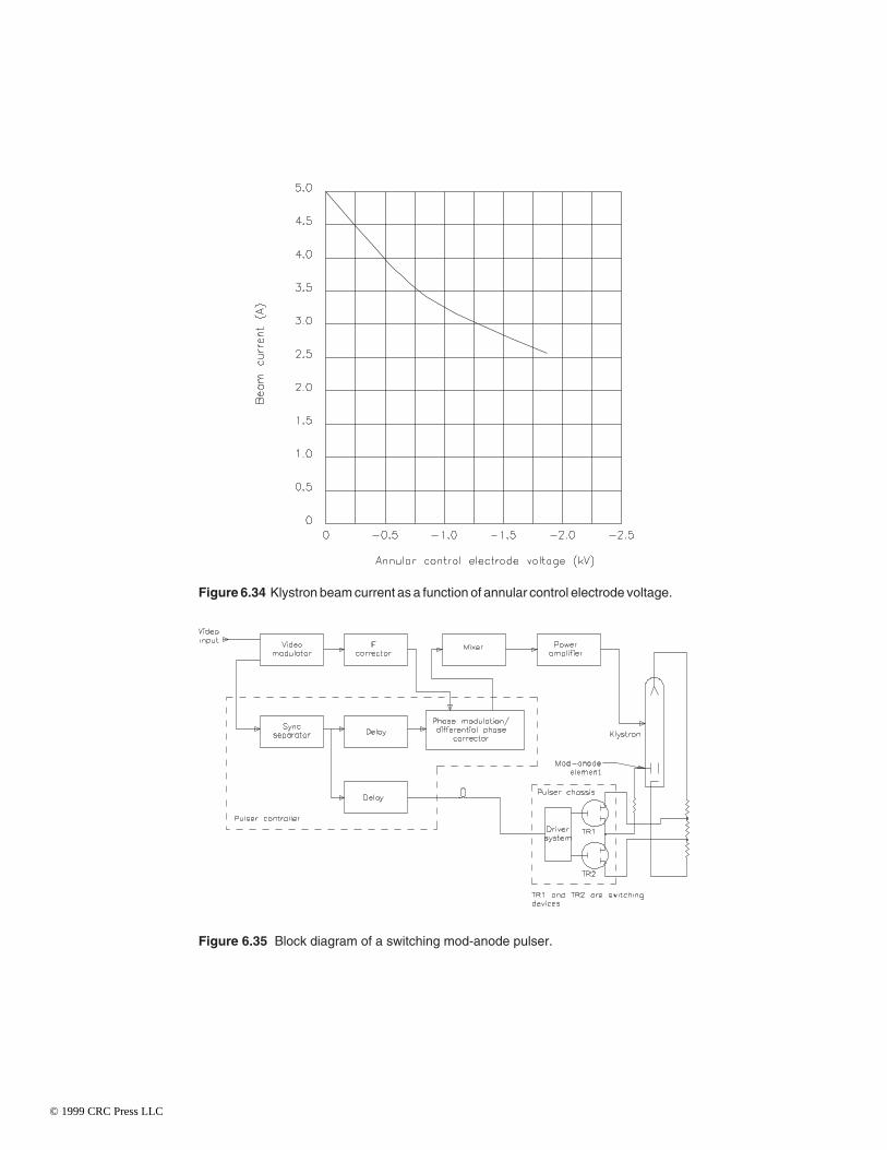
Figure 6.35 Block diagram of a switching mod-anode pulser.
Figure 6.34 Klystron beam current as a function of annular control electrode voltage.
© 1999 CRC Press LLC

uum envelope. High-efficiency integral- and external-cavity klystrons have been de-signed to provide maximum conversion performance consistent with signal bandwidthrequirements. The saturated conversion efficiency is essentially identical for integral-or external-cavity klystrons with equal numbers of resonant cavities.
Number of Cavities
The relative benefits of integral- vs. external-cavity klystrons can be debated atlength. Discussion typically centers on operating efficiency, life expectancy, and re-placement device cost. In a comparison of the efficiency of integral- vs. external-cav-ity klystrons for UHF-TV applications, however, the question really boils down to thenumber of cavities (four or five) used in the device. Four-cavity external tubes arestandard. It is usually not practical to produce high-power five-cavity external tubesfor mechanical and electrical (voltage standoff) reasons.
Integral devices permit the addition of a fifth cavity to the design for two primaryreasons. First, the device itself is mechanically more robust. The addition of a fifth cav-ity to an external klystron increases the length and weight of the device. Because of thesize of the drift tube in an external device designed for UHF-TV frequencies, the addi-tional weight is difficult to support. Second, because the cavities are enclosed in a vac-uum in the integral design, voltage standoff problems are greatly reduced.
The tuning mechanism of an integral-cavity klystron is enclosed in a rigid steelshell. In the external-cavity unit, the tuning mechanism is in air. Within the region of thetuning mechanism, RF fields can reach high levels, especially at the high end of theUHF-TV band. The highest energy field occurs in the area of the last cavity. Because ofthe high dielectric properties of a vacuum, dielectric breakdown is less of a problem inthe integral design, which places the tuning mechanism within a vacuum envelope.This situation is of particular concern at the high end of the UHF band, where the spac-ing of tuning elements is closer.
Four-cavity integral-type klystrons are manufactured, but for power outputs of 30kW or less. The 60 kW integral klystron, typically used for UHF-TV broadcasting, isproduced as a five-cavity design.
The physics of the integral- and external-cavity klystrons are essentially the same. Ina comparison of integral and external units of like design—that is, with the same num-ber of cavities—performance should be identical. The two units follow the same lawsof physics and use basically the same components up to the beam stick. It is when man-ufacturers take advantage of the relative merits of each design that differences in per-formance are realized.
Efficiency
For the sake of comparison, the data presented in this section will assume:
• The power level is 60 kW
• All integral-cavity devices utilize five cavities
• All external-cavity devices utilize four cavities
© 1999 CRC Press LLC

The five-cavity integral S-tuned klystron is inherently at least 20 percent more effi-cient than a four-cavity tube. (S-tuning refers to the method of stagger tuning the cavi-ties.) The five-cavity klystron generally is specified by the manufacturer for a mini-mum efficiency of 52 percent (saturated efficiency). Typical efficiency is 55 percent.Four-cavity devices are characteristically specified at 42 percent minimum and 45 per-cent typical.
This efficiency advantage is possible because the fifth cavity of the integral designpermits tuning patterns that allow maximum transfer of RF energy while maintainingadequate bandpass response. Tighter bunching of electrons in the beam stick, a func-tion of the number of cavities, also contributes to the higher efficiency operation. In ac-tuality, the fifth cavity allows design engineers to trade gain for efficiency. Still, thefive-cavity tube has significantly more gain than the four-cavity device. The five-cav-ity unit, therefore, requires less drive, which simplifies the driving circuit. A five-cav-ity klystron requires approximately 25 W of drive power, while a four-cavity tube needsas much as 90 W for the same power output.
Under pulsed operation, approximately the same reduction in beam current is real-ized with both integral- and external-cavity klystrons. In a comparison of peak-of-syncFOM, the efficiency differences will track. There is, fundamentally, no reason that onetype of klystron should pulse differently than the other.
Performance Tradeoffs
It is the designer’s choice whether to build a transmitter with the klystron cavities lo-cated inside or outside the vacuum envelope. There are benefits and drawbacks toeach approach.
When the cavity resonators are a part of the tube, the device becomes more compli-cated and more expensive. However, the power generating system is all together in onepackage, which simplifies installation significantly.
When the resonator is separate from the tube, as in an external-cavity device, it canbe made with more compliance (greater room for adjustment). Consequently, a singledevice may be used over a wider range of operating frequencies. In terms of UHF-TV, asingle external-cavity device may be tuned for operation over the entire UHF-TV band.This feature is not possible if the resonant cavities are built into the device. To cover theentire UHF-TV band, three integral-cavity tubes are required. The operational divi-sions are:
• Channels 14 to 29 (470 to 566 MHz)
• Channels 30 to 51 (566 to 698 MHz)
• Channels 52 to 69 (698 to 746 MHz)
This practical limitation to integral-cavity klystron construction may be a drawbackfor some facilities. For example, it is not uncommon for group operations to share oneor more spare klystrons. If the facilities have operating frequencies outside the limits ofa single integral device, it may be necessary to purchase more than one spare. Also,
© 1999 CRC Press LLC

when the cavities are external, the resonators are in air and can be accessed to permitfine adjustments of the tuning stages for peak efficiency.
The advantages of tube changing are significant with an integral device. Typicaltube change time for an integral klystron is 1 hour, as opposed to 4 to 6 hours for an ex-ternal device. The level of experience of the technician is also more critical when an ex-ternal-type device is being changed. Tuning procedures must be carefully followed bymaintenance personnel to avoid premature device failure.
6.3.6 MSDC Klystron
Developmental work on the multistage depressed collector (MSDC) klystron began inthe mid-1980s. The project1 produced a working tube capable of efficiency in UHFservice that had been impossible with previous klystron-based technology.
The MSDC device may be used in a number of varied applications. NASA originallybecame involved in the project as a way to improve the efficiency of satellite transmit-ters. With limited power available onboard a space vehicle, efficient operation is criti-cally important. Such transmitters traditionally operate in a linear, inefficient mode.UHF-TV broadcasters were interested in the MSDC because it promised to reduce thehuge operating costs associated with high-power operation.
Experimentation with depressed collector klystrons dates back to at least the early1960s. Early products offered a moderate improvement in efficiency, but at the price ofgreater mechanical and electrical complexity. The MSDC design, although mechani-cally complex, offers a significant gain in efficiency.
Theory of Operation
MSDC tubes have been built around both integral-cavity and external-cavity kly-strons. The devices are essentially identical to a standard klystron, except for the col-lector assembly. Mathematical models provided researchers with detailed informationon the interactions of electrons in the collector region. Computer modeling also pro-vided the basis for optimization of a beam-reconditioning scheme incorporated intothe device. Beam reconditioning is achieved by including a transition region betweenthe RF interaction circuit and the collector under the influence of a magnetic field. Itis interesting to note that the mathematical models made for the MSDC project trans-lated well into practice when the actual device was constructed.
From the electrical standpoint, the more stages of a multistage depressed collectorklystron, the better. The tradeoff, predictably, is increased complexity and, therefore,increased cost for the product. There is also a point of diminishing returns that isreached as additional stages are added to the depressed collector system. A four-stagedevice was chosen for TV service because of these factors. As more stages are added(beyond four), the resulting improvement in efficiency is proportionally smaller.
1 A joint effort of the National Aeronautics and Space Administration (NASA), severalUHF-TV transmitter manufacturers, Varian Associates, and other concerns.
© 1999 CRC Press LLC

Figure 6.36 shows the mechanical configuration of the four-stage MSDC klystron.Note the “V” shape that was found, through computer modeling, to provide the bestcapture performance, minimizing electron feedback. A partially assembled collectorassembly is shown in Figure 6.37.
Because the MSDC device is identical to a conventional klystron except for the col-lector, efficiency improvement techniques used for klystrons can be incorporated intothe MSDC. ACE-type pulsing commonly is used to improve efficiency in TV applica-tions. Figure 6.38 illustrates the effects of ACE voltage on beam current.
Electron Trajectories
The dispersion of electrons in the multistage collector is the key element in recoveringpower from the beam and returning it to the power supply. This is the mechanism thatpermits greater operating efficiency from the MSDC device.
Figure 6.39 illustrates the dispersion of electrons in the collector region during a car-rier-only operating mode. Note that there is little dispersion of electrons between stagesof the MSDC. Most are attracted to electrode 4, the element at the lowest potential(6.125 kV), referenced to the cathode.
Figure 6.36 Mechanical design of the multistage depressed collector assembly. Notethe “V” shape of the 4-element system.
© 1999 CRC Press LLC
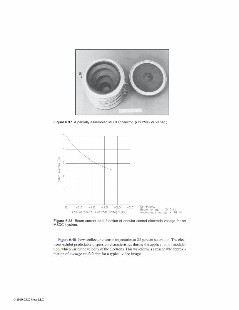
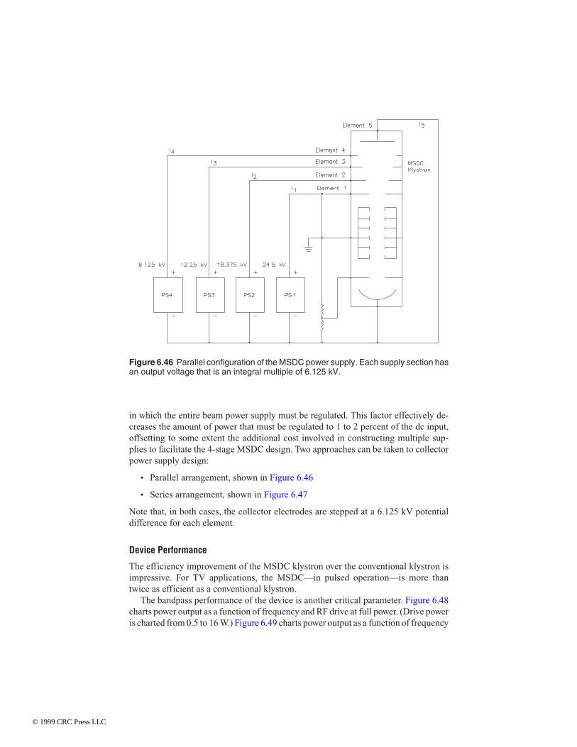
Figure 6.40 shows collector electron trajectories at 25 percent saturation. The elec-trons exhibit predictable dispersion characteristics during the application of modula-tion, which varies the velocity of the electrons. This waveform is a reasonable approxi-mation of average modulation for a typical video image.
Figure 6.37 A partially assembled MSDC collector. (Courtesy of Varian.)
Figure 6.38 Beam current as a function of annular control electrode voltage for anMSDC klystron.
© 1999 CRC Press LLC
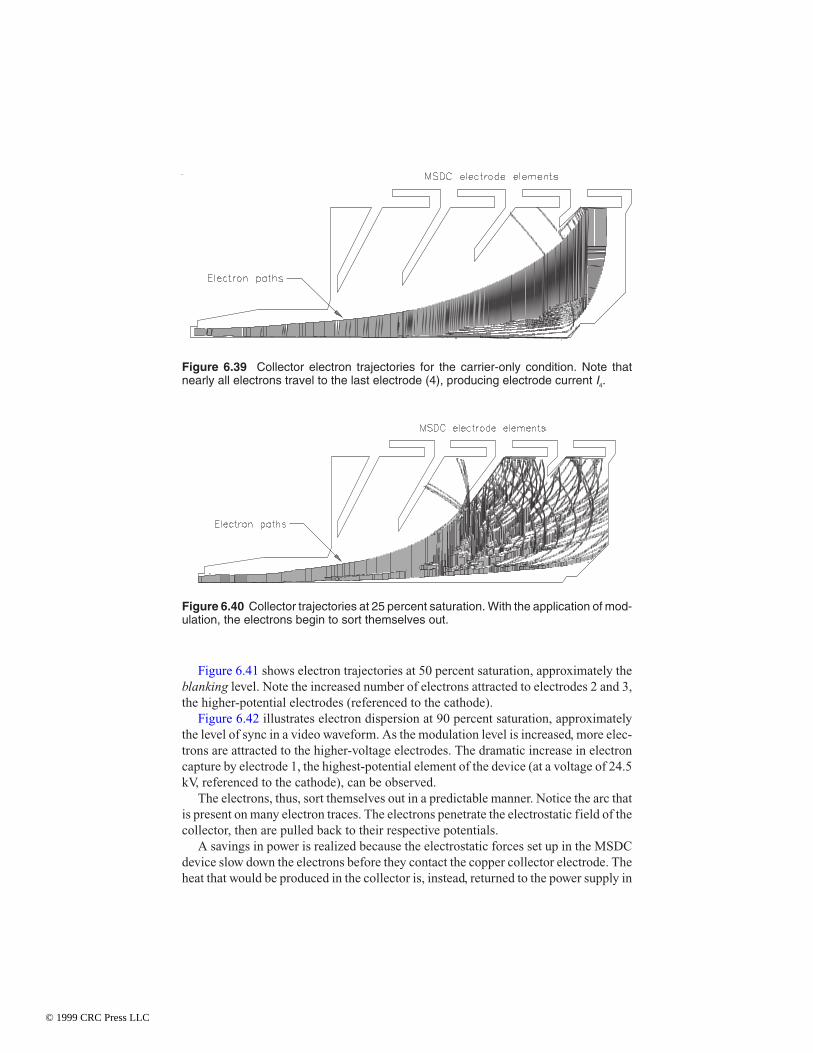
Figure 6.41 shows electron trajectories at 50 percent saturation, approximately theblanking level. Note the increased number of electrons attracted to electrodes 2 and 3,the higher-potential electrodes (referenced to the cathode).
Figure 6.42 illustrates electron dispersion at 90 percent saturation, approximatelythe level of sync in a video waveform. As the modulation level is increased, more elec-trons are attracted to the higher-voltage electrodes. The dramatic increase in electroncapture by electrode 1, the highest-potential element of the device (at a voltage of 24.5kV, referenced to the cathode), can be observed.
The electrons, thus, sort themselves out in a predictable manner. Notice the arc thatis present on many electron traces. The electrons penetrate the electrostatic field of thecollector, then are pulled back to their respective potentials.
A savings in power is realized because the electrostatic forces set up in the MSDCdevice slow down the electrons before they contact the copper collector electrode. Theheat that would be produced in the collector is, instead, returned to the power supply in
Figure 6.39 Collector electron trajectories for the carrier-only condition. Note thatnearly all electrons travel to the last electrode (4), producing electrode current I4.
Figure 6.40 Collector trajectories at 25 percent saturation. With the application of mod-ulation, the electrons begin to sort themselves out.
© 1999 CRC Press LLC

the form of electric energy. In theory, peak efficiency would occur if the electrons wereslowed down to zero velocity. In practice, however, that is not possible.
Figure 6.43 shows the distribution of collector current as a function of drive power.With no RF drive, essentially all current goes to electrode 4, but as drive is increased, I4
drops rapidly as collector current is distributed among the other elements. Note that thecurrent to electrode 5 (cathode potential) peaks at about 10 percent of beam current.This suggests that the secondary yield of the collector surfaces is within acceptable lim-its.
Inserted between the klystron and the collector assembly is a refocusing electromag-net that controls the electron beam as it enters the collector region.
Figure 6.41 Collector electron trajectories at 50 percent saturation, approximately theblanking level. The last three electrodes (2, 3, and 4) share electrons in a predictablemanner, producing currents I2, I3, and I4.
Figure 6.42 Collector trajectories at 90 percent saturation, the sync level. Note the sig-nificant increase in the number of electrons attracted to the first electrode, producing I1.
© 1999 CRC Press LLC

Mechanical Construction
The completed MSDC assembly is shown in Figure 6.44 with the collector shield par-tially removed to allow visibility of the collector elements. The collector of thefour-stage MSDC design actually is composed of five elements mounted between ce-ramic rings for electrical insulation. The fifth electrode is at cathode potential.
Cooling for the MSDC is, not surprisingly, more complicated than for a conven-tional klystron. The tradeoff, however, is that there is less heat to remove because of thehigher efficiency of the device. Water cooling is provided on each electrode of theMSDC tube.
Figure 6.45 illustrates the overall mechanical design of an external-cavity version ofthe MSDC tube, including placement of the device in its cavity bay.
Although the MSDC has not been in service for a sufficient length of time to com-pletely characterize the product life expectancy, researchers believe that the MSDC de-sign will have little, if any, effect on the lifetime of the klystron. The electron beam is es-sentially unchanged. The tube is identical to a conventional integral- or external-cavityklystron except in collector assembly.
Figure 6.43 The distribution of electrode current as a function of drive power. Note thesignificant drop in I4 as drive power is increased. I5 is the electrode at cathode potential.
© 1999 CRC Press LLC

MSDC Power Supply
Design criteria for the collector power supply system provide a mixed bag of require-ments. The critical parameter is the degree of regulation between the cathode and an-ode. The relative differences between the elements of the collector are not, in most ap-plications, significant. Consequently, the bulk of the power supplied to the tube doesnot need to be well regulated. This is in contrast with conventional klystron operation,
Figure 6.44 The MSDC collector assembly withthe protective shield partially removed. (Courtesyof Varian.)
Figure 6.45 Mechanical construction of an external-cavity MSDC tube: (a) device, (b)device in cavity assembly.
(a) (b)
© 1999 CRC Press LLC
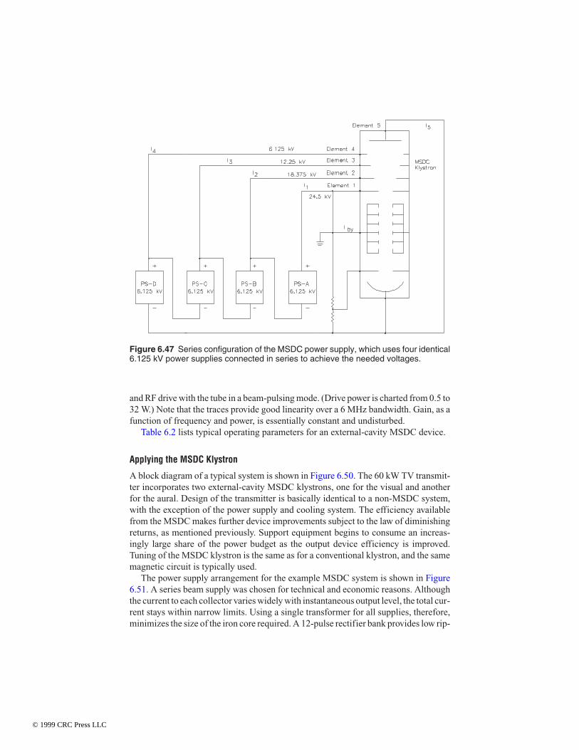
in which the entire beam power supply must be regulated. This factor effectively de-creases the amount of power that must be regulated to 1 to 2 percent of the dc input,offsetting to some extent the additional cost involved in constructing multiple sup-plies to facilitate the 4-stage MSDC design. Two approaches can be taken to collectorpower supply design:
• Parallel arrangement, shown in Figure 6.46
• Series arrangement, shown in Figure 6.47
Note that, in both cases, the collector electrodes are stepped at a 6.125 kV potentialdifference for each element.
Device Performance
The efficiency improvement of the MSDC klystron over the conventional klystron isimpressive. For TV applications, the MSDC—in pulsed operation—is more thantwice as efficient as a conventional klystron.
The bandpass performance of the device is another critical parameter. Figure 6.48charts power output as a function of frequency and RF drive at full power. (Drive poweris charted from 0.5 to 16 W.) Figure 6.49 charts power output as a function of frequency
Figure 6.46 Parallel configuration of the MSDC power supply. Each supply section hasan output voltage that is an integral multiple of 6.125 kV.
© 1999 CRC Press LLC
and RF drive with the tube in a beam-pulsing mode. (Drive power is charted from 0.5 to32 W.) Note that the traces provide good linearity over a 6 MHz bandwidth. Gain, as afunction of frequency and power, is essentially constant and undisturbed.
Table 6.2 lists typical operating parameters for an external-cavity MSDC device.
Applying the MSDC Klystron
A block diagram of a typical system is shown in Figure 6.50. The 60 kW TV transmit-ter incorporates two external-cavity MSDC klystrons, one for the visual and anotherfor the aural. Design of the transmitter is basically identical to a non-MSDC system,with the exception of the power supply and cooling system. The efficiency availablefrom the MSDC makes further device improvements subject to the law of diminishingreturns, as mentioned previously. Support equipment begins to consume an increas-ingly large share of the power budget as the output device efficiency is improved.Tuning of the MSDC klystron is the same as for a conventional klystron, and the samemagnetic circuit is typically used.
The power supply arrangement for the example MSDC system is shown in Figure6.51. A series beam supply was chosen for technical and economic reasons. Althoughthe current to each collector varies widely with instantaneous output level, the total cur-rent stays within narrow limits. Using a single transformer for all supplies, therefore,minimizes the size of the iron core required. A 12-pulse rectifier bank provides low rip-
Figure 6.47 Series configuration of the MSDC power supply, which uses four identical6.125 kV power supplies connected in series to achieve the needed voltages.
© 1999 CRC Press LLC

Figure 6.48 Device bandwidth as a function of frequency and drive power. Beam volt-age is 24.5 kV, and beam current is 5.04 A for an output power of 64 kW. These tracesrepresent the full-power test of the MSDC device.
Figure 6.49 Device bandwidth in the beam-pulsing mode as a function of frequencyand drive power. Beam voltage is 24.5 kV, and beam current is 3.56 A with an outputpower of 34.8 kW.
© 1999 CRC Press LLC

ple and reduces the need for additional filtering. The size and complexity of the recti-fier stack are increased little beyond a normal beam supply because the total potentialof the four supplies is similar to that of a normal klystron transmitter (24.5 to 27.5 kV).
The collector stages of the MSDC device are water-cooled by a single water paththat loops through each electrode element. Because high voltage is present on the indi-vidual elements, purity of the water is critical to proper operation. A two-stage systemis used with a water-to-water plate heat exchanger separating the primary and second-ary systems.
6.4 Klystrode/Inductive Output Tube (IOT)The Klystrode tube is the result of a development program started in 19802 withUHF-TV in mind as a primary application. The basic concept of the Klystrode datesback to the late 1930s,3 but it was not until the early 1980s that serious engineering ef-fort was put into the tube to make it a viable product for high-power UHF service. Thefundamental advantage of the Klystrode, also known as the inductive output tube
Table 6.2 Typical Operating Parameters for an External-Cavity MSDC Klystron forUHF-TV service (Courtesy of Varian.)
Parameter Typical ValueOperating frequency (visual) 519 MHzOutput power, peak-of-sync 64 kWDrive power, peak-of-sync 20 WGain, peak-of-sync 35 dBFigure of merit 1.31
Bandwidth, –1 dB 6 MHzBeam voltage 24.5 kVBeam current 5.3 ABody current 50 mA dcModulating-anode voltage 19.5 kV dcModulating-anode current 0.5 mA dcFocusing current 11 A dcIon pump voltage 3.2 kV dcLoad VSWR > 1.1:1Refocusing coil current 7 A dcRefocusing coil voltage 10 V dc
1 Figure of merit is equal to the quotient of peak-of-sync output power and the average dc beaminput power.
2 Varian/Eimac3 Andrew Haeff, 1938
© 1999 CRC Press LLC

Figure 6.51 Simplified schematic diagram of the power supply for an MSDC klystrontransmitter. A single high-voltage transformer with multiple taps is used to provide theneeded collector voltage potentials.
Figure 6.50 Simplified block diagram of a 60 kW (TVT) MSDC transmitter. The auralklystron may utilize a conventional or MSDC tube at the discretion of the user.
© 1999 CRC Press LLC

(IOT), is its ability to operate class B. The result is higher efficiency when comparedwith a conventional klystron.
6.4.1 Theory of Operation
As its name implies, the Klystrode tube is a hybrid between a klystron and a tetrode.The high reliability and power-handling capability of the klystron is due, in part, tothe fact that electron beam dissipation takes place in the collector electrode, quite sep-arate from the RF circuitry. The electron dissipation in a tetrode is at the anode andthe screen grid, both of which are an inherent part of the RF circuit and, therefore,must be physically small at UHF frequencies. The tetrode, however, has the advantagethat modulation is produced directly at the cathode by a grid so that a long drift spaceis not required to produce density modulation. The Klystrode/IOT has a similar ad-vantage over the klystron—high efficiency in a small package [4]. The Klystrode tubeis a registered trademark of Varian. The IOT is the generic description for the device,and it will be used in this discussion.
The IOT is shown schematically in Figure 6.52. The electron beam is formed at thecathode, density-modulated with the input RF signals by a grid, then acceleratedthrough the anode aperture. In its bunched form, the beam drifts through a field-free re-gion, then interacts with the RF field in the output cavity. Power is extracted from thebeam in the same way as in a klystron. The input circuit resembles that of a typical UHFpower grid tube. The output circuit and collector resemble those in a klystron.
A production version of a 60 kW device is shown in Figure 6.53. Double-tuned cavi-ties are used to obtain the required operating bandwidth. The load is coupled at the sec-ond cavity, as shown in Figure 6.54. This arrangement has proved to be an attractiveway to couple power out of the device because no coupling loop or probe is required inthe primary cavity, which can be a problem at the high end of the UHF band.
Because the IOT provides both beam power variation during sync pulses (as in apulsed klystron) and variation of beam power over the active modulating waveform, it iscapable of high efficiency. The device provides full-time beam modulation as a resultof its inherent structure and class B operation.
6.4.2 Electron Gun
Many design elements from the klystron have been borrowed for use in the IOT [4]. Abarium aluminate cathode is used for the gun, taken from a conventional klystron to-gether with its heater structure. The methods used to support the cathode, heater, andnecessary heat shields in the klystron gun have been retained for use in the IOT. Fig-ure 6.55 shows the construction of the IOT gun and output cavity.
In the IOT, the RF input voltage is applied between the cathode and a grid that allowsextra electrons to be drawn from the cathode into a low-quiescent-current electronbeam according to the instantaneous RF voltage appearing between the grid and cath-ode. The resulting density-modulated beam is then passed into the klystron-like RFoutput interaction region of the tube.
© 1999 CRC Press LLC

The grid is clamped in place in front of the cathode, supported on a metal cylinder,and isolated from the cathode by a ceramic insulator. A second ceramic insulator sup-ports the complete gridded electron gun at the correct distance from the grounded an-
Figure 6.53 A 60 kW Klystrode tube mounted inits support stand with the output cavity attached.(Courtesy of Varian.)
Figure 6.52 Simplified schematic diagram of the Klystrode tube.
© 1999 CRC Press LLC

ode. This ceramic insulator completes the vacuum envelope and holds off the full beamvoltage of approximately 30 kV. The IOT gun operates at cathode-to-anode voltages ap-proximately 50 percent higher than those of conventional klystron guns. Stray capaci-tance in the grid support structure has been minimized to reduce losses.
The grid-to-cathode space of the electron gun forms the end of a long and complexRF transmission line from the RF input connector of the input cavity system. This de-sign has a significant effect upon the final frequency range of the IOT input cavity. Be-cause the grid-to-cathode distance is crucial to the physics of the device, the grid re-quires a rigid support structure to maintain proper spacing at high operating tempera-tures.
6.4.3 Grid Structure
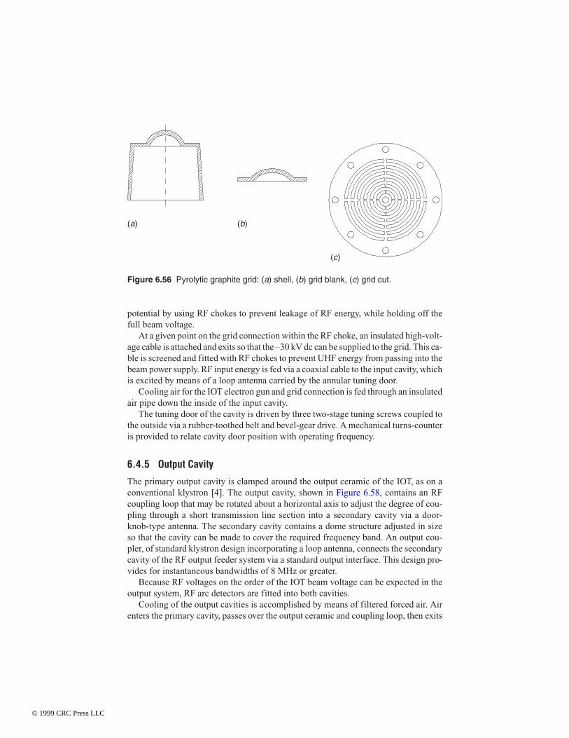
A pyrolytic graphite grid is used in the IOT because of its strength and its ability tomaintain desired specifications at elevated temperatures [4]. Pyrolytic graphite has aunique advantage over other common grid materials in that its strength increases asthe temperature climbs to 2500°C and above, whereas the strength of pure metals uni-versally decreases as the temperature increases. This allows the designer to produce athin grid, with fine grid wires that may be accurately positioned and will retain theirposition and shape when raised to operating temperatures of approximately 1000°C.
During production of the grid, a hydrocarbon, typically methane, is fed into alow-pressure chamber containing a graphite rod of the correct form to produce the re-quired graphite shell. A shell typically consists of a graphite cylinder with a closed,shaped end. The cold gas is passed into a hot zone in the reactor, which is heated by anRF eddy current system from outside the vessel. An ordered carbon structure, as op-posed to an amorphous structure, is required. To provide the needed processing, thetemperature of the reactor is set to approximately 2000°C at a pressure of 10 torr. Thegraphite shells produced in this way have a layered structure with anisotropic propertiesand are physically durable.
Figure 6.54 A close-up view of thedouble-tuned output cavity of a 60 kWKlystrode tube. (Courtesy of Varian.)
© 1999 CRC Press LLC

The shells are then machined to the desired shape and size, and holes are cut into theresulting grid back using a laser under computer control. The process of producing apyrolytic graphite grid is illustrated in Figure 6.56.
6.4.4 Input Cavity
Although similar, the Klystrode and the IOT are not identical. There are both subtleand significant differences in each design. The greatest departure can be seen in theconfiguration of the input cavity [4]. The design of the IOT is shown in Figure 6.57. Acylindrical resonant cavity containing an annular sliding tuning door is used. The cav-ity is folded at the IOT electron gun end to make contact with the tube via an RFchoke structure. Because both the cathode and grid operate at beam potential (30 kV),it is necessary to maintain the body of the cavity and its tuning mechanism at ground
Figure 6.55 Overall structure of the IOT gun and output cavity. (After [4].)
© 1999 CRC Press LLC
potential by using RF chokes to prevent leakage of RF energy, while holding off thefull beam voltage.
At a given point on the grid connection within the RF choke, an insulated high-volt-age cable is attached and exits so that the –30 kV dc can be supplied to the grid. This ca-ble is screened and fitted with RF chokes to prevent UHF energy from passing into thebeam power supply. RF input energy is fed via a coaxial cable to the input cavity, whichis excited by means of a loop antenna carried by the annular tuning door.
Cooling air for the IOT electron gun and grid connection is fed through an insulatedair pipe down the inside of the input cavity.
The tuning door of the cavity is driven by three two-stage tuning screws coupled tothe outside via a rubber-toothed belt and bevel-gear drive. A mechanical turns-counteris provided to relate cavity door position with operating frequency.
6.4.5 Output Cavity
The primary output cavity is clamped around the output ceramic of the IOT, as on aconventional klystron [4]. The output cavity, shown in Figure 6.58, contains an RFcoupling loop that may be rotated about a horizontal axis to adjust the degree of cou-pling through a short transmission line section into a secondary cavity via a door-knob-type antenna. The secondary cavity contains a dome structure adjusted in sizeso that the cavity can be made to cover the required frequency band. An output cou-pler, of standard klystron design incorporating a loop antenna, connects the secondarycavity of the RF output feeder system via a standard output interface. This design pro-vides for instantaneous bandwidths of 8 MHz or greater.
Because RF voltages on the order of the IOT beam voltage can be expected in theoutput system, RF arc detectors are fitted into both cavities.
Cooling of the output cavities is accomplished by means of filtered forced air. Airenters the primary cavity, passes over the output ceramic and coupling loop, then exits
Figure 6.56 Pyrolytic graphite grid: (a) shell, (b) grid blank, (c) grid cut.
(a) (b)
(c)
© 1999 CRC Press LLC

via holes in the coupling hub assembly into the secondary cavity. After cooling the sec-ondary cavity, some of the air exits via the contact fingers on the tuning doors, while asmall portion traverses the output loop and coupler, exiting at a stub-pipe fitting for thatpurpose.
Typical operating parameters for the IOT are shown in Table 6.3.
6.4.6 Application Considerations
An active crowbar circuit is included in most applications of the Klystrode/IOT toprotect the pyrolytic graphite grid in the event of an arc condition inside the tube [4].The crowbar provides the added benefit of reducing the amount of gas generated inthe tube during an arc. A block diagram of a typical crowbar is shown in Figure 6.59.The response time of the crowbar is typically less than 10 µs. The peak current per-missible through the discharge tube may be 3000 A or greater.
Because of the IOT’s class B operation, the response of the power supply to a vary-ing load is an important design parameter. If a standard klystron beam supply were usedin an IOT-equipped RF generator, performance under varying modulation levels could
Figure 6.57 IOT input cavity. (After [4].)
© 1999 CRC Press LLC

be unacceptable. Consider the application of a bounce (black-to-white) signal to a TVtransmitter. Beam current for a typical IOT 60 kW transmitter would change from ap-proximately 400 mA to 2 A. The effect with a conventional klystron supply would beringing of about 20 percent on the beam voltage. The IOT power supply, therefore, mustbe designed for tight transient regulation.
Table 6.3 Typical Operating Parameters of the IOT in TV Service
Parameter Typical ValueBeam voltage 28 kVMean beam current 1.15 APeak beam current 2.50 AGrid bias –72 VGrid current 1 mABody current 6 mAInput power 399 WOutput power 40.3 kW
Figure 6.58 IOT output cavity. (After [4].)
© 1999 CRC Press LLC

The IOT does not have the same hard saturation characteristic as a klystron. TheIOT’s high-power transfer curve flattens more slowly than a klystron’s and continues toincrease with increasing drive power, requiring a different approach to linearity correc-tion.
6.4.7 Continuing Research Efforts
Several variations on the basic Klystrode/IOT theme have been developed, includingair-cooled devices operating at 30 kW and above. Air cooling is practical at thesepower levels because of the improved efficiency that class B operation provides.
Research also is being conducted to extend the operating power of the IOT to 500kW or more. Designed for scientific research applications, such devices offer numer-ous benefits over conventional klystron technology. The IOT is much smaller than aklystron of similar power, and it requires less support circuitry. Because of the im-proved efficiency, power supply requirements are reduced, and device cooling is sim-plified.
Figure 6.59 Simplified block diagram of the crowbar circuit designed into the KlystrodeSK-series (Comark) transmitters. The circuit is intended to protect the tube from poten-tially damaging fault currents.
© 1999 CRC Press LLC

6.5 Constant Efficiency AmplifierBecause of the similarity between the spent electron beam in an IOT and that of a kly-stron or traveling-wave tube, it is possible to consider the use of a multistage de-pressed collector on an IOT to improve the operating efficiency [5]. This had beenconsidered by Priest and Shrader [6] and by Gilmore [7], but the idea was rejected be-cause of the complexity of the multistage depressed collector assembly and becausethe IOT already exhibited fairly high efficiency. Subsequent development by Symons[5, 8] has led to a prototype device (at this writing). An inductive output tube, modi-fied by the addition of a multistage depressed collector, has the interesting property ofproviding linear amplification with (approximately) constant efficiency.
6.5.1 Theory of Operation
Figure 6.60 shows a schematic representation of the constant efficiency amplifier(CEA) [5]. The cathode, control grid, anode and output gap, and external circuitry areessentially identical with those of the IOT amplifier. Drive power introduced into theinput cavity produces an electric field between the control grid and cathode, whichdraws current from the cathode during positive half-cycles of the input RF signal. For
Figure 6.60 Schematic overview of the MSDC IOT or constant efficiency amplifier. (Af-ter [5].)
© 1999 CRC Press LLC

operation as a linear amplifier, the peak value of the current—or more accurately, thefundamental component of the current—is made (as nearly as possible) proportionalto the square root of the drive power, so that the product of this current and the voltageit induces in the output cavity will be proportional to the drive power.
Following the output cavity is a multistage depressed collector in which several typi-cal electron trajectories are shown. These are identified by the letters a through e. Thecollector electrodes are connected to progressively lower potentials between the anodepotential and the cathode potential so that more energetic electrons penetrate moredeeply into the collector structure and are gathered on electrodes of progressively lowerpotentials.
In considering the difference between an MSDC IOT and an MSDC klystron, it isimportant to recognize that in a class B device, no current flows during the portion ofthe RF cycle when the grid voltage is below cutoff and the output gap fields are acceler-ating. As a result, it is not necessary to have any collector electrode at a potential equalto or below cathode potential. At low output powers, when the RF output gap voltage isjust equal to the difference in potential between the lowest-potential collector electrodeand the cathode, all the current will flow to that electrode. Full class B efficiency is thusachieved under these conditions.
As the RF output gap voltage increases with increased drive power, some electronswill have lost enough energy to the gap fields so they cannot reach the lowest potentialcollector, and so current to the next-to-the-lowest potential electrode will start increas-ing. The efficiency will drop slightly and then start increasing again until all the currentis just barely collected by the two lowest-potential collectors, and so forth.
Maximum output power is reached when the current delivered to the output gap issufficient to build up an electric field or voltage that will just stop a few electrons. Atthis output power, the current is divided between all of the collector electrodes and theefficiency will be somewhat higher than the efficiency of a single collector, class B am-plifier. Computer simulations have demonstrated that it is possible to select the collec-tor voltages so as to achieve very nearly constant efficiency from the MSDC IOT deviceover a wide range of output powers [5].
The challenge of developing a multistage depressed collector for an IOT is not quitethe same as that of developing a collector for a conventional klystron [8]. It is differentbecause the dc component of beam current rises and falls in proportion to the squareroot of the output power of the tube. The dc beam current is not constant as it is in a kly-stron (or a traveling-wave tube for that matter). As a result, the energy spread is low be-cause the output cavity RF voltage is low at the same time that the RF and dc beam cur-rents are low. Thus, there will be small space-charge forces, and the beam will notspread as much as it travels deep into the collector toward electrodes having the lowestpotential. For this reason, the collector is likely to be rather long and thin when com-pared to the multistage depressed collector for a conventional klystron, as describedpreviously.
Figure 6.61 charts the calculated efficiency for an IOT with six depressed collectorstages, set at 0.1, 0.2, 0.3, 0.45, 0.7, and 1.0 times the beam voltage (compared to that ofa conventional IOT).
© 1999 CRC Press LLC

6.6 Traveling Wave TubeThe traveling wave tube (TWT) is a linear-beam device finding extensive applicationsin communications and research. Power levels range from a few watts to 10 MW. Gainranges from 40 to 70 dB for small drive signals. The TWT consists of four basic ele-ments:
• Electron gun. The gun forms a high-current-density beam of electrons that inter-act with a wave traveling along the RF circuit to increase the amplitude of the RFsignal. In a typical application, electrons are emitted from a cathode and con-verged to the proper beam size by focusing electrodes.
• RF interaction circuit. The RF wave is increased in amplitude as a result of inter-action with the electron beam from the gun. The fundamental principle on whichthe TWT operates is that an electron beam, moving at approximately the same ve-locity as an RF wave traveling along a circuit, gives up energy to the RF wave.
• Magnetic electron beam focusing system. The beam size is maintained at theproper dimensions through the interaction structure by the focusing system. Thismay be accomplished by using either a permanent magnet or an electromagneticfocusing element.
• Collector. The electron beam is received at the collector after it has passedthrough the interaction structure. The remaining beam energy is dissipated in thecollector.
Figure 6.61 Calculated efficiency of an MSDC IOT compared to an unmodified IOT.(After [5].)
© 1999 CRC Press LLC

Figure 6.62 shows the basic elements of a TWT.The primary differences between types of TWT devices involve the RF interaction
structure employed. In Figure 6.62, the interaction structure is a helix. A variety ofother structures may be employed, depending on the operating power and frequency.Three common approaches are used to provide the needed magnetic beam focusing. Il-lustrated in Figure 6.63, they are:
• Electromagnetic focusing, used primarily on high-power tubes, where tight beamfocusing is required.
• Permanent-magnet focusing, used where the interaction structure is short.
• Periodic permanent-magnet focusing, used on most helix TWT and coupled-cav-ity tubes. The magnets are arranged with alternate polarity in successive cellsalong the interaction region.
6.6.1 Theory of Operation
The interaction structure acts to slow the RF signal so that it travels at approximatelythe same speed as the electron beam. Electrons enter the structure during both posi-tive and negative portions of the RF cycle. Electrons entering during the positive por-tion are accelerated; those entering during the negative portion are decelerated. Theresult is the creation of electron bunches that produce an alternating current superim-posed on the dc beam current. This alternating current induces the growth of an RFcircuit wave that encourages even tighter electron bunching.
One or more severs are included to absorb reflected power that travels in a backwarddirection on the interaction circuit. This reflected power is the result of a mismatch be-tween the output port and the load. Without the sever, regenerative oscillations couldoccur.
Figure 6.62 Basic elements of a traveling wave tube.
© 1999 CRC Press LLC

At a given frequency, a particular level of drive power will result in maximumbunching and power output. This operating point is referred to as saturation.
Interaction Circuit
The key to TWT operation lies in the interaction element. Because RF waves travel atthe speed of light, a method must be provided to slow down the forward progress ofthe wave to approximately the same velocity as the electron beam from the cathode.The beam speed of a TWT is typically 10 to 50 percent the speed of light, correspond-ing to cathode voltages of 4 to 120 kV. Two mechanical structures commonly are usedto slow the RF wave:
• Helix circuit. The helix is used where bandwidths of an octave or more are re-quired. Over this range the velocity of the signal carried by the helix is basicallyconstant with frequency. Typical operating frequencies range from 500 MHz to40 GHz. Operating power, however, is limited to a few hundred watts. TWTs in-tended for higher-frequency operation may use a variation of the helix, shown inFigure 6.64. The ring-loop and ring-bar designs permit peak powers of hundredsof kilowatts. The average power, however, is about the same as that of a conven-tional helix because the structure used to support the interaction circuit is thesame.
Figure 6.63 Magnetic focusing for a TWT: (a) solenoid-type, (b) perma-nent-magnet-type, (c) periodic permanent-magnet structure.
(a) (b)
(c)
© 1999 CRC Press LLC

• Coupled-cavity circuit. The coupled-cavity interaction structure permits opera-tion at high peak and average power levels, and moderate bandwidth (10 percentbeing typical). TWTs using coupled-cavity structures are available at operatingfrequencies from 2 to 100 GHz. The basic design of a coupled-cavity interactioncircuit is shown in Figure 6.65. Resonant cavities, coupled through slots cut in thecavity end walls, resemble a folded waveguide. Two basic schemes are used: thecloverleaf and the single-slot space harmonic circuit.
The cloverleaf, also known as the forward fundamental circuit, is used primarily onhigh-power tubes. The cloverleaf provides operation at up to 3 MW peak power and 5kW average at S-band frequencies. The single-slot space harmonic interaction circuit ismore common than the cloverleaf. The mechanical design is simple, as shown in thefigure. The single-slot space harmonic structure typically provides peak power of up to50 kW and average power of 5 kW at X-band frequencies.
Pulse Modulation
The electron beam from the gun may be pulse-modulated using one of four methods:
• Cathode pulsing. The cathode is pulsed in a negative direction with respect to thegrounded anode. This approach requires the full beam voltage and current to beswitched.
• Anode pulsing. This approach is similar to cathode pulsing, except that the fullbeam voltage is switched between cathode potential and ground. The currentswitched, however, is only that value intercepted on the anode. Typically, the in-tercepted current is a few percent of the full beam potential.
Figure 6.64 Helix structures for a TWT: (a) ring-loop circuit, (b) ring-bar circuit.
(a)
(b)
© 1999 CRC Press LLC

• Focus electrode pulsing. If the focus electrode, which normally operates at ornear cathode potential, is biased negatively with respect to the cathode, the beamwill be turned off. The voltage swing required is typically one-third of the fullcathode voltage. This approach is attractive because the focus electrode draws es-sentially no current, making implementation of a switching modulator relativelyeasy.
• Grid pulsing. The addition of a grid to the cathode region permits control of beamintensity. The voltage swing required for the grid, placed directly in front of thecathode, is typically 5 percent of the full beam potential.
Electron Gun
The electron gun of a TWT is a device that supplies the electron beam to the tube [9].A schematic diagram of a generic electron gun is given in Figure 6.66. The deviceconsists of a hot cathode heated by an electric heater, a negatively biased focusingelectrode or focuser, and a positively biased accelerating anode. The cross-sectionalview given in the figure can be a two-dimensional or three-dimensional coaxial struc-ture [10, 11].
An axially symmetrical solid cylindrical electron beam is produced by the gun struc-ture shown in Figure 6.66 if the structure is axially cylindrically symmetrical. If themiddle of the hot cathode is made nonemitting and only the edge of the cathode is emit-ting, the cathode becomes an annular cathode [9]. The annular cathode produces a hol-low beam. The annular electron beam can be used to reduce beam current for a givenmicrowave output power.
If the gun structure shown in Figure 6.66 is two dimensional, then a ribbon-shapedelectron beam is produced. A ribbon-shaped beam is used for a TWT of a two-dimen-sional structure.
Figure 6.65 Coupled-cavity interaction structures: (a) forward fundamental circuit or“cloverleaf,” (b) single-slot space harmonic circuit.
(a) (b)
© 1999 CRC Press LLC
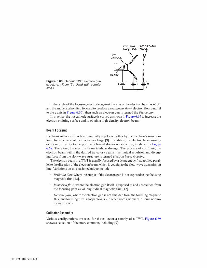
If the angle of the focusing electrode against the axis of the electron beam is 67.5°and the anode is also tilted forward to produce a rectilinear flow (electron flow parallelto the z axis in Figure 6.66), then such an electron gun is termed the Pierce gun.
In practice, the hot cathode surface is curved as shown in Figure 6.67 to increase theelectron emitting surface and to obtain a high-density electron beam.
Beam Focusing
Electrons in an electron beam mutually repel each other by the electron’s own cou-lomb force because of their negative charge [9]. In addition, the electron beam usuallyexists in proximity to the positively biased slow-wave structure, as shown in Figure6.68. Therefore, the electron beam tends to diverge. The process of confining theelectron beam within the desired trajectory against the mutual repulsion and diverg-ing force from the slow-wave structure is termed electron beam focusing.
The electron beam in a TWT is usually focused by a dc magnetic flux applied paral-lel to the direction of the electron beam, which is coaxial to the slow-wave transmissionline. Variations on this basic technique include:
• Brillouin flow, where the output of the electron gun is not exposed to the focusingmagnetic flux [12].
• Immersed flow, where the electron gun itself is exposed to and unshielded fromthe focusing para-axial longitudinal magnetic flux [12].
• Generic flow, where the electron gun is not shielded from the focusing magneticflux, and focusing flux is not para-axia. (In other words, neither Brillouin nor im-mersed flow.)
Collector Assembly
Various configurations are used for the collector assembly of a TWT. Figure 6.69shows a selection of the more common, including [9]:
Figure 6.66 Generic TWT electron gunstructure. (From [9]. Used with permis-sion.)
© 1999 CRC Press LLC

• Plate collector
• Cone collector
• Curved cone
• Cylinder collector
• Depressed potential cylinder
• Two-stage collector
• Three-stage collector
Cooling options include conduction, air, and water.
Figure 6.68 Generic configuration of a traveling wave tube. (From [9]. Used with per-mission.)
Figure 6.67 Cross-sectional view of a TWTelectron gun with a curved hot cathode.(From [9]. Used with permission.)
© 1999 CRC Press LLC

Cooling of a low-power TWT is accomplished by clamping the tube to a metal base-plate, mounted in turn on an air- or liquid-cooled heat sink. Coupled-cavity tubes below1 kW average power are convection-cooled by circulating air over the entire length ofthe device. Higher-power coupled-cavity tubes are cooled by circulating liquid over thetube body and collector.
6.6.2 Operating Efficiency
Efficiency is not one of the TWT’s strong points. Early traveling wave tubes offeredonly about 10 percent dc-to-RF efficiency. Wide bandwidth and power output arewhere the TWT shines. TWT efficiency may be increased in two basic ways: (1) col-lector depression for a single-stage collector, or (2) use of a multistage collector.
Collector depression refers to the practice of operating the collector at a voltagelower than the full beam voltage. This introduces a potential difference between the in-teraction structure and the collector, through which electrons pass. The amount bywhich a single-stage collector can be depressed is limited by the remaining energy ofthe slowest electrons. In other words, the potential reduction can be no greater than theamount of energy of the slowest electrons, or they will turn around and reenter the inter-action structure, causing oscillations.
By introducing multiple depressed collector stages, still greater efficiency can berealized. This method provides for the collection of the slowest electrons at one collec-tor potential, while allowing those with more energy to be collected on other stages thatare depressed still further. This approach, similar to the MSDC design discussed previ-ously, is illustrated in Figure 6.70.
Figure 6.69 Cross-sectional view of various collector configurations for a TWT. (From[9]. Used with permission.)
© 1999 CRC Press LLC
6.6.3 Operational Considerations
Although traveling wave tubes offer numerous benefits to the end user, they are notwithout their drawbacks.
Intermodulation Distortion
TWTs are susceptible to intermodulation (IM) distortion when multiple carriers areintroduced, as in double illuminated or multiple SCPC (single channel per carrier)satellite transponders. These IM products may be found at frequencies that are dis-placed from the fundamental carriers by the difference in frequency between them.When multiple carriers are present, the potential for IM exists. This potential is re-duced by operating the TWT below saturation. Power must be reduced (backed off) inproportion to the number of carriers and their relative power.
Second-Harmonic Content
Because of the wide bandwidth and nonlinear operating characteristics under satura-tion conditions, a TWT may generate significant second-harmonic energy. It is notuncommon to measure second-harmonic energy at the output of a TWT that is downonly 10 dB from the operating carrier.
Figure 6.70 Power supply configuration for a multistage depressed collector TWT.
© 1999 CRC Press LLC

Reduction of harmonic content usually involves injecting a coherent harmonic sig-nal with controlled phase and amplitude along with the fundamental carrier so that theyinteract, minimizing harmonic energy at the output of the device.
AM/PM Conversion
AM/PM conversion is the change in phase angle between the input and output signalsas the input varies in amplitude. The root cause of this distortion in a TWT centers onthe reduction of electron beam velocity as the input signal level increases. This causesa greater energy exchange between the electron beam and the RF wave. At a level 20dB below the input power required for saturation, AM/PM conversion is negligible.At higher levels, AM/PM distortion may increase.
Phase Variation
When the velocity of the electron beam in the TWT is changed, the phase of the out-put signal also will vary. The primary causes of beam velocity variations includechanges in one or more of the following:
• Cathode temperature
• Grid voltage
• Anode voltage
• Cathode voltage
The TWT power supply must be well regulated (to less than 0.2 percent) to preventbeam velocity changes that may result in output signal phase variations.
6.7 Crossed-Field TubesA crossed-field microwave tube is a device that converts dc into microwave energyusing an electronic energy-conversion process. These devices differ from beam tubesin that they are potential-energy converters, rather than kinetic-energy converters.The term crossed field is derived from the orthogonal characteristics of the dc electricfield supplied by the power source and the magnetic field required for beam focusingin the interaction region. This magnetic field typically is supplied by a perma-nent-magnet structure. Such devices also are referred to as M-tubes.
Practical devices based on the crossed-field principles fall into two broad catego-ries:
• Injected-beam crossed-field tubes. The electron stream is produced by an elec-tron gun located external to the interaction region, similar to a TWT. The conceptis illustrated in Figure 6.71.
• Emitting-sole tubes. The electron current for interaction is produced directlywithin the interaction region by secondary electron emissions, which result whensome electrons are driven to the negative electrode and allowed to strike it. The
© 1999 CRC Press LLC

negative electrode is formed using a material capable of producing significantnumbers of secondary-emission electrons. The concept is illustrated in Figure6.72.
6.7.1 Magnetron
The magnetron encompasses a class of devices finding a wide variety of applications.Pulsed magnetrons have been developed that cover frequency ranges from the lowUHF band to 100 GHz. Peak power from a few kilowatts to several megawatts hasbeen obtained. Typical overall efficiencies of 30 to 40 percent may be realized, de-pending on the power level and operating frequency. CW magnetrons also have beendeveloped, with power levels of a few hundred watts in a tunable tube, and up to 25kW or more in a fixed-frequency device. Efficiencies range from 30 percent to asmuch as 70 percent.
The magnetron operates electrically as a simple diode. Pulsed modulation is ob-tained by applying a negative rectangular voltage waveform to the cathode with the an-ode at ground potential. Operating voltages are less critical than for beam tubes;line-type modulators often are used to supply pulsed electric power. The physical struc-ture of a conventional magnetron is shown in Figure 6.73.
High-power pulsed magnetrons are used primarily in radar systems. Low-powerpulsed devices find applications as beacons. Tunable CW magnetrons are used in ECM(electronic countermeasures) applications. Fixed-frequency devices are used as micro-wave heating sources.
Figure 6.71 Linear injected-beam microwave tube.
© 1999 CRC Press LLC

Tuning of conventional magnetrons is accomplished by moving capacitive tuners orby inserting symmetrical arrays of plungers into the inductive portions of the device.Tuner motion is produced by a mechanical connection through flexible bellows in thevacuum wall. Tuning ranges of 10 to 12 percent of bandwidth are possible for pulsedtubes, and as much as 20 percent for CW tubes.
Operating Principles
Most magnetrons are built around a cavity structure of the type shown in Figure 6.74.The device consists of a cylindrical cathode and anode, with cavities in the anode thatopen into the cathode-anode space—the interaction space—as shown. Power can becoupled out of the cavities by means of a loop or a tapered waveguide.
Cavities, together with the spaces at the ends of the anode block, form the resonantsystem that determines the frequency of the generated oscillations. The actual shape ofthe cavity is not particularly important, and various types are used, as illustrated in Fig-ure 6.75. The oscillations associated with the cavities are of such a nature that alternat-ing magnetic flux lines pass through the cavities parallel to the cathode axis, while thealternating electric fields are confined largely to the region where the cavities open intothe interaction space. The most important factors determining the resonant frequencyof the system are the dimensions and shape of the cavities in a plane perpendicular tothe axis of the cathode. Frequency also is affected by other factors such as the end spaceand the axial length of the anode block, but to a lesser degree.
Figure 6.72 Reentrant emitting-sole crossed-field amplifier tube.
© 1999 CRC Press LLC

Figure 6.73 Conventional magnetron structure.
(a) (b)
Figure 6.74 Cavity magnetron oscillator: (a) cutaway view, (b) cross section view per-pendicular to the axis of the cathode.
© 1999 CRC Press LLC

The magnetron requires an external magnetic field with flux lines parallel to the axisof the cathode. This field usually is provided by a permanent-magnet or electromagnet.
The cathode is commonly constructed as a cylindrical disk.
Coaxial Magnetron
The frequency stability of a conventional magnetron is affected by variations in theload impedance and by cathode-current fluctuations. Depending on the extent ofthese two influences, the magnetron occasionally may fail to produce a pulse. The co-axial magnetron minimizes these effects by using the anode geometry shown in Fig-ure 6.76. Alternate cavities are slotted to provide coupling to a surrounding coaxialcavity.
The oscillating frequency is controlled by the combined vane system and the reso-nant cavity. Tuning may be accomplished through the addition of a movable end plate inthe cavity, as shown in Figure 6.77.
Frequency-Agile Magnetron
Tubes developed for specialized radar and ECM applications permit rapid tuning ofthe magnetron. A conventional device may be tuned using one of the following meth-ods:
• A rapidly rotating capacitive element. Tubes of this type are referred to asspin-tuned magnetrons.
• A hydraulic-driven tuning mechanism. Tubes of this type are referred to as me-chanically tuned magnetrons.
Electronic tuning of magnetrons is also possible, with tuning rates as high as severalmegahertz per microsecond.
(a) (b) (c)
Figure 6.75 Cavity magnetron oscillator anode: (a) hole-and-slot type, (b) slot type, (c)vane type.
© 1999 CRC Press LLC

Figure 6.76 Structure of a coaxial magnetron.
Figure 6.77 Structure of a tunable coaxial magnetron.
© 1999 CRC Press LLC

Linear Magnetron
Although the most common types of magnetrons are radial in nature, the linear mag-netron and inverted magnetron may also be used, depending upon the application[13]. A cross-sectional view of a linear magnetron is given in Figure 6.78. Shown inthe figure is the O-type linear magnetron, in which the electron beam emitted fromthe electron gun is focused by a longitudinally applied dc magnetic flux density (B),as in the case of the traveling wave tube.
As shown in the figure, a number of slots are included in the basic structure. Theseslots are cut 1/4-wavelength deep, functioning as quarter-wave cavity resonators. Thisstructure forms a series of microwave cavity resonators coupling to an electron beam,in a similar manner to the multicavity klystron. The velocity modulated electrons arebunched, and the tightly bunched electrons produce amplified microwave energy at theoutput cavity, which is coupled to an external circuit. The linear magnetron typically of-fers high gain, but narrow frequency bandwidth.
6.7.2 Backward Wave Oscillator
In a traveling wave tube, if the microwave signal to be amplified is propagating in theslow-wave structure backwardly to the direction of the electron beam, the device istermed a backward wave oscillator (BWO) [13]. Microwaves traveling in a backwarddirection carry positive feedback energy toward the electron gun and yield strongervelocity modulation and bunching. Thus, the system is inherently an oscillator ratherthan a stable amplifier. The input is typically terminated by an impedance-matchedreflectionless termination device. The oscillation frequency is a function of the speedof the electrons and the time constant of the feedback mechanism. The speed of elec-tron motion is controlled by the anode voltage.
An M-type radial BWO is shown in Figure 6.79. The direction of electron pole mo-tion and the direction of microwave propagation along the annular reentrant type
Figure 6.78 Cross-sectional view of a linear magnetron. (From [13]. Used with permis-sion.)
© 1999 CRC Press LLC

slow-wave structure are opposite each other. It should be noted that the depths of theslits cut in the inner surface of the anode is very shallow—much less than 1/4-wave-length deep. In other words, the slits are not in resonance; they are not cavity resonators,as is the case of a magnetron. Rather, the slits are nonresonating, as in the case of aTWT. In the M-type radial BWO, the electron beam is focused by a magnetic flux den-sity applied perpendicular to the beam, as seen from Figure 6.79.
An M-type radial BWO is sometimes termed the Carcinotron, a trade name. A keyfeature of the Carcinotron is its wide voltage tunability over a broad frequency range.
6.7.3 Strap-Fed Devices
A radial magnetron can be configured so that every other pole of the anode resonatorsare conductively tied for microwave potential equalization, as shown in Figure 6.80a[13]. These conducting tie rings are termed straps; the technique of using strap ringsis termed strapping. Strapping ensures good synchronization of microwaves in themagnetron resonators with the rotation of electron poles.
The technique of strapping is extended and modified for an M-type radial BWO, asshown in Figure 6.80b. Strapping rings tie every other pole of the radial slow-wavestructure, as in the case of a strapped radial magnetron, but the strapping rings are nolonger reentrant. Microwave energy to be amplified is fed to the strap at one end, andthe amplified output is extracted from the other end. This type of electron tube istermed a strap-fed device.
If an M-type radial BWO is strapped, usually it does not start oscillation by itself.But, if microwave energy is fed through the strap from the outside using an external mi-crowave power source to the microwave input, then the oscillation starts—and even if
Figure 6.79 Functional schematic of the M-type radial BWO. (From [13]. Used with per-mission.)
© 1999 CRC Press LLC

the exciter source is turned off, the oscillation continues. This type of M-type radialBWO is termed the platinotron [14].
In a platinotron, if the output of the tube is fed back to the input through a high-Qcavity resonator, it becomes a self-starting oscillator. The oscillation frequency is stabi-lized by the high-Q cavity resonator. This type of high-power frequency stabilizedstrapped radial BWO is termed the stabilotron [14]. The operating powers are at kilo-watt and megawatt levels.
Performance of the platinotron depends on, among other things, the design of theslow-wave structure. For example, the interdigital slow-wave structure as shown in Fig-ure 6.80 has a limited power handling capability and frequency bandwidth. Design of aslow-wave structure with greater power handling capacity and stability, with broaderfrequency bandwidth, is possible. For example, instead of an anode with an interdigitalslow-wave structure, the anode could be made of an annular open conducting duct,loaded with a number of pairs of conducting posts across the open duct. Strapping isdone at every other tip of the pairs of conducting posts. This type of strapping loads theslow-wave structure, stabilizing it and preventing oscillation. The structure of the an-ode with an annular duct and pairs of posts increases the power handling capability.This type of loaded radial BWO is termed the amplitron [14, 10]. The amplitron is capa-ble of amplifying high-power microwave signals with pulses and continuous waves. Itis used for long-range pulsed radar transmitter amplifiers and industrial microwaveheating generators. The operating power levels range from kilowatt to megawatt levels.
Figure 6.80 Strap-fed devices: (a) strapped radial magnetron, (b) nonreentrant strap-ping of a BWO. (From [13]. Used with permission.)
(a) (b)
© 1999 CRC Press LLC
6.7.4 Gyrotron
The gyrotron is a cyclotron resonance maser.4 The device includes a cathode, collec-tor, and circular waveguide of gradually varying diameter. Electrons are emitted at thecathode with small variations in speed. The electrons then are accelerated by an elec-tric field and guided by a static magnetic field through the device. The nonuniforminduction field causes the rotational speed of the electrons to increase. The linear ve-locity of the electrons, as a result, decreases. The interaction of the microwave fieldwithin the waveguide and the rotating (helical) electrons causes bunching similar tothe bunching within a klystron. A decompression zone at the end of the device per-mits decompression and collection of the electrons.
The power available from a gyrotron is 100 times greater than that possible from aclassic microwave tube at the same frequency. Power output of 100 kW is possible at100 GHz, with 30 percent efficiency. At 300 GHz, up to 1.5 kW may be realized, butwith only 6 percent efficiency.
Theory of Operation
The trajectory of an electron in an electron beam focused by a longitudinally appliedmagnetic field is a helix [13]. If the electron velocity, electron injection angle, and ap-plied longitudinal magnetic flux density are varied, then an electron beam of helicalform with different size and pitch will be formed. A coil-shaped electron beam will beproduced by adjusting the acceleration voltage, applied magnetic flux density, and theelectron injection angle to the focusing magnetic field. The coil of the electron beamcan be a simple single coil, or—depending on the adjustment of the aforementionedthree parameters—it can be an electron beam of a double coil, or a large coil made ofthin small coils. In the case of the double-coil trajectory, the large coil-shaped trajec-tory is termed the major orbit and smaller coil trajectory is termed the minor orbit.
If a single coil-shaped electron beam is launched in a waveguide, as shown in Figure6.81, then microwaves in the waveguide will interact with the helical beam. This type ofvacuum tube is termed the helical beam tube [14]. In this class of device, a single-coilhelical beam is launched into a TE10 mode rectangular waveguide. Inside the wave-guide, microwaves travel from right to left and the helical beam travels in an oppositedirection. Therefore, the microwave-electron beam interaction is of the backward wavetype. If the microwave frequency, the focusing magnetic flux density B, and the acceler-ation voltage Va are properly adjusted, this device will function as a backward wave am-plifier. Electrons in the helical beam interact with the transverse microwave electricfields and are velocity modulated at the left-hand side of the waveguide as the beam en-ters into the waveguide. The velocity modulated electrons in the helical beam arebunched as they travel toward the right. If the alternating microwave electric field syn-
4 Maser is an acronym for microwave amplification by simulated emission of radiation. Maseris a general class of microwave amplifiers based on molecular interaction withelectromagnetic radiation.
© 1999 CRC Press LLC

chronizes its period and phase with the helical motion of bunched electrons so that theelectrons always receive retardation from microwave transverse electric fields, then theelectrons lose their kinetic energy and the microwave signal gains in electric field en-ergy according to the principle of kinetic energy conservation. Thus, the amplified mi-crowave power emerges at the waveguide output at the left (because the microwavestravel backward).
In Figure 6.81, if the microwave input port and the output port are interchanged witheach other, then the system becomes a forward wave amplifier. Such a forward waveamplifier is termed a peniotron [14].
If the electron gun is modified to incorporate a side emitting cathode and the wave-guide is changed to TE11 mode oversized circular waveguide, as shown in Figure 6.82a,the gyrotron is formed. In this device, both ends of the waveguide are open and there aresufficient reflections in the waveguide for positive feedback. The gyrotron is, thus, aforward wave oscillator.
A double-coil helical beam gyrotron is shown in Figure 6.82b. The device is formedby readjusting the anode voltage and the focusing flux density so that the electron beamis made into a double helical coil (as shown in the figure), and operating the oversizedcircular waveguide in the TE01 mode. In the TE01 mode, the microwave transverse elec-tric fields exist as concentric circles. Therefore, the tangential electric fields interactwith electrons in the small coil trajectory. The alternating tangential microwave electricfields are made to synchronize with the tangential motion of electrons in the minorcoil-shaped trajectory. Thus, electron velocity modulation takes place near the cathodeand bunching takes place in the middle of the tube. Microwave kinetic energy transfertakes place as the beam approaches the right. The focusing magnetic flux density B isapplied only in the interaction region. Therefore, if the electron beam comes out of theinteraction region, it is defocused and collected by the anode waveguide (as depicted inFigure 6.82b). If the circular waveguide is operated in an oversized TE11 mode, with thedouble-coil helical beam, then the device is referred to as a tornadotron [14]. Micro-wave-electron interaction occurs between the parallel component of tangential motionof the small helical trajectory and the TE11 mode microwave electric field. If the phaseof microwave electric field decelerates bunched electrons, then the lost kinetic energyof the bunched electrons is transferred to the microwave signal and oscillation begins.
Figure 6.81 Basic structure of ahelical beam tube. (From [13].Used with permission.)
© 1999 CRC Press LLC

Gyrotron Design Variations
The gyrotron exists in a number of design variations, each optimized for a particularfeature or application [13, 15, 16].
When the gyrotron circular waveguide is split as shown in Figure 6.83, the tube istermed the gyroklystron amplifier [13]. Both waveguides resonate to the input fre-quency, and there are strong standing waves in both waveguide resonators. The inputmicrowave signal to be amplified is fed through a side opening to the input waveguideresonator. This is the buncher resonator, which functions in a manner similar to the kly-stron. The buncher resonator imparts velocity modulation to gyrating electrons in thedouble helical coil-shaped electron beam. There is a drift space between the buncherresonator and the catcher resonator at the output. While drifting electrons bunch andbunched electrons enter into the output waveguide catcher resonator, electron speed isadjusted in such a manner that electrons are decelerated by the resonating microwaveelectric field. This lost kinetic energy in bunched electrons is transformed into micro-wave energy and microwaves in the catcher resonator are, thus, amplified. The ampli-fied power appears at the output of the tube.
If the gyrotron waveguide is an unsplit one-piece waveguide that is imped-ance-matched and not resonating, as shown in Figure 6.84, the tube is termed thegyrotron traveling wave tube amplifier [13]. In this tube, the input microwaves are fedthrough an opening in the waveguide near the electron gun. Microwaves in the wave-
(a)
(b)
Figure 6.82 Functional schematic diagram of the gyrotron: (a) single coiled helicalbeam gyrotron, (b) electron trajectory of double-coil helical beam gyrotron. (From [13].Used with permission.)
© 1999 CRC Press LLC

guide are amplified gradually as they travel toward the output port by interacting withthe double-coiled helical electron beam, which is velocity-modulated and bunched.There are no significant standing waves in the waveguide. Microwaves grow graduallyin the waveguide as they travel toward the output port as a result of interaction with elec-trons.
If the electron gun of the gyrotron is moved to the side of the waveguide and micro-wave power is extracted from the waveguide opening in proximity to the electron gun,as shown in Figure 6.85, then the device is termed a gyrotron backward oscillator [13].The principle involved is similar to the backward wave oscillator, and the process of ve-locity modulation, drifting, bunching, and catching is similar to that of the klystron.Microwave energy induced in the waveguide travels in both directions, but the circuit isadjusted to emphasize the waves traveling in a backward direction. The backwardwaves become the output of the tube and, at the same time, carry the positive feedbackenergy to the electrons just emitted and to be velocity-modulated. The system, thus,goes into oscillation.
Figure 6.83 Basic structure of the gyroklystron amplifier. (From [13]. Used with permis-sion.)
Figure 6.84 Basic structure of the gyroklystron traveling wave tube amplifier. (From[13]. Used with permission.)
© 1999 CRC Press LLC

If the gyrotron waveguide is split into two again, but this time the input side wave-guide is short and the output side waveguide is long, as shown in Figure 6.86, then thetube is termed a gyrotwystron amplifier [13]. This device is a combination of thegyroklystron and gyrotron traveling wave tube amplifier, thus the name gyrotwystronamplifier. The input side waveguide resonator is the same as the input resonator wave-guide of a gyroklystron. There are strong standing waves in the input bunched-wave-guide resonator. There is no drift space between the two waveguides. The output sidewaveguide is a long impedance-matched waveguide and there is no microwave stand-ing wave in the waveguide (a traveling-wave waveguide). As microwaves travel in thewaveguide, they interact with bunched electrons and the microwaves grow as theymove toward the output port.
6.8 Other Microwave DevicesThere are a number of variations on the basic microwave devices outlined previouslyin this chapter. Some find widespread usage, others have little commercial interest.
Figure 6.85 Basic structure of the gyrotron backward oscillator. (From [13]. Used withpermission.)
Figure 6.86 Basic structure of the gyrotwystron amplifier. (From [13]. Used with permis-sion.)
© 1999 CRC Press LLC

Among the important specialty device classifications are quasiquantum devices andmodified klystrons.
6.8.1 Quasiquantum Devices
In a gyrotron, if electrons are accelerated by extremely high voltage, they become rel-ativistic [13]. That is, the mass of an electron becomes a function of the velocity as,
( )m
m
cv
=−
0
2
1
(6.3)
Where:m = the relativistic mass of an electronm0 = the static mass of an electronc = the speed of light in vacuumv = the speed of the electron in question
The energy states of electrons are specified by a set of quantum numbers, and thetransition of energy states occurs only between those numbers so described. A set ofquantum numbers specifies the high-energy orbit and low-energy orbit of an electron.
One device based on this principle is the free electron laser, or the ubitron [13]. Aschematic diagram of the device is given in Figure 6.87. A high-speed relativistic elec-tron beam is emitted from an electron gun focused by a longitudinally applied dc mag-netic flux density B and is periodically deflected by magnetic means. The repetitiousdeflections create among relativistic electrons high-energy states and low-energystates. If the high-energy electrons in the deflection waveguides are stimulated by theresonance frequency of the waveguide resonator, then the downward transition (thetransition of electrons in a high-energy state to a low-energy state) occurs. Microwaveemissions result because of the energy transitions at the stimulation frequency.
The ubitron operates at millimeter or submillimeter wave frequencies, and typicallyat high power levels.
6.8.2 Variations on the Klystron
Because the multiple cavities of a conventional klystron are difficult to fabricate atmillimeter wavelengths, variations on the basis design have been produced [13]. In-stead of using multiple cavity resonators, the cavities can instead be combined into asingle cavity. Such a design can be accomplished through the use of ladder-shapedgrids, as shown in Figure 6.88a by the dashed lines with the single cavity. This type ofklystron is referred to as the laddertron [14]. Because of the ladder structure, a stand-ing wave will exist on on the ladder line. Velocity modulation results near the electrongun and bunching begins near the middle of the electron stream. Catching is done inthe ladder structure near the collector. Because this device is a one-cavity resonator,
© 1999 CRC Press LLC

there is built-in positive feedback. Oscillation, therefore, begins in a manner similarto a reflex klystron, also a single cavity tube.
At millimeter wavelengths, a dominant mode cavity resonator becomes very smalland loses its power-handling capability. In a laddertron, however, the cavity resonator isa multiple higher-mode resonator. Therefore, the Q of the cavity is high and the size ofthe cavity resonator is reasonably large. This being the case, the laddertron can handletens of watts of power at frequency as high as 50 GHz.
The catcher of a two-cavity klystron amplifier can be replaced by the slow-wavestructure of a traveling wave tube, as shown in Figure 6.88b. This type of tube is termedthe twystron [14]. The slow-wave structure provides a broader frequency bandwidththan a regular two-cavity klystron. A microwave input signal fed into the buncher cavityresults in velocity modulation of the electron beam. Bunching occurs while the beamdrifts, and the bunched electrons induce a microwave voltage in the slow-wave struc-ture. The electron beam is focused by the use of longitudinally applied magnetic fluxdensity B.
Figure 6.87 Basic structure of the ubitron. (From [13]. Used with permission.)
Figure 6.88 Functional schematic diagrams of modified klystrons: (a) laddertron, (b)twystron. (From [13]. Used with permission.)
(a) (b)
© 1999 CRC Press LLC

Commercial twystrons typically operate at 2–6 GHz and are used in pulsed radartransmitter power amplifiers. Pulsed peak output powers range from 1 to 7 MW (pulsewidth of 10–50 µs) [10].
6.9 Microwave Tube LifeAny analysis of microwave tube life must first identify the parameters that define life.The primary wear-out mechanism in a microwave power tube is the electron gun atthe cathode. In principle, the cathode eventually will evaporate the activating materialand cease to produce the required output power. Tubes, however, rarely fail because oflow emission, but for a variety of other reasons that are usually external to the device.
Power tubes designed for microwave applications provide long life when operatedwithin their designed parameters. The point at which the device fails to produce the re-quired output power can be predicted with some accuracy, based on design data andin-service experience. Most power tubes, however, fail because of mechanisms otherthan predictable chemical reactions inside the device itself. External forces, such astransient overvoltages caused by lightning, cooling system faults, and improper tuning,more often than not lead to the failure of a microwave tube.
6.9.1 Life-Support System
Transmitter control logic usually is configured for two states of operation:
• An operational level, which requires all of the “life-support” systems to be pres-ent before the high-voltage (HV) command is enabled.
• An overload level, which removes HV when one or more fault conditions occur.
The cooling system is the primary life-support element in most RF generators. Thecooling system should be fully operational before the application of voltages to thetube. Likewise, a cool-down period usually is recommended between the removal ofbeam and filament voltages and shutdown of the cooling system.
Most microwave power tubes require a high-voltage removal time of less than 100ms after the occurrence of an overload. If the trip time is longer, damage to the devicemay result. Arc detectors often are installed in the cavities of high-power tubes to sensefault conditions and shut down the high-voltage power supply before damage can bedone to the tube. Depending on the circuit parameters, arcs can be sustaining, requiringremoval of high voltage to squelch the arc. A number of factors can cause RF arcing, in-cluding:
• Overdrive condition
• Mistuning of one or more cavities
• Poor cavity fit (applies to external types only)
• Undercoupling of the output to the load
• Lightning strike at the antenna
© 1999 CRC Press LLC

• High VSWR
Regardless of the cause, arcing can destroy internal elements or the vacuum seal ifdrive and/or high voltage are not removed quickly. A lamp usually is included witheach arc detector photocell for test purposes.
6.9.2 Protection Measures
A microwave power tube must be protected by control devices in the amplifier sys-tem. Such devices offer either visual indications or aural alarm warnings, or they ac-tuate interlocks within the system. Figure 6.89 shows a klystron amplifier and the ba-sic components associated with its operation, including metering for each of thepower supplies. Other types of microwave power devices use similar protectionschemes. Sections of coaxial transmission line, representing essential components,are shown in the figure attached to the RF input and RF output ports of the tube. Asingle magnetic coil is shown to represent any coil configuration that may exist; itsposition in the drawing is for convenience only and does not represent its true positionin the system.
Heater Supply
The heater power supply can be either ac or dc. If it is dc, the positive terminal mustbe connected to the common heater-cathode terminal and the negative terminal to thesecond heater terminal. The amount of power supplied to the heater is important be-cause it establishes the cathode operating temperature. The temperature must be highenough to provide ample electron emission, but not so high that emission life is jeop-ardized.
Because the cathode and heater are connected to the negative side of the beam sup-ply, they must be insulated to withstand the full beam potential. This dictates the use ofa filament transformer designed specifically for the specific application.
Beam Supply
The high-voltage beam supply furnishes the dc input power to the microwave device.In a klystron, the positive side of the beam supply is connected to the body and collec-tor. The negative terminal is connected to the common heater-cathode terminal. Neverconnect the negative terminal of the beam supply to the heater-only terminal becausethe beam current will then flow through the heater to the cathode and cause prematureheater failure. The voltmeter, Eb in Figure 6.89, measures the beam voltage appliedbetween the cathode and the body of the klystron.
Current meter Ic measures collector current, typically 95 percent or more of the totaldevice current. Current meter Iby measures body current. An interlock should interruptthe beam supply if the body current exceeds a specified maximum value.
The sum of the body current (Iby) and collector current (Ic) is equal to the beam cur-rent (Ib), which should stay constant as long as the beam voltage and modulating-anodevoltage are held constant.
© 1999 CRC Press LLC

Magnet Supply
Electrical connections to the dc magnet supply typically include two meters, one formeasuring current through the circuit (Im in Figure 6.89), and one for measuring volt-age (Em). When a microwave device is installed in its magnet assembly, both parame-ters should be measured and recorded for future reference. If excessive body currentor other unusual symptoms occur, this data will be valuable for system analysis.
Undercurrent protection should be provided to remove beam voltage if the magneticcircuit current falls below a preset value. The interlock also should prevent the beamvoltage from being applied if the magnetic circuit is not energized. This scheme, how-ever, will not provide protection if windings of the magnet are short-circuited.Short-circuited conditions can be determined by measuring the normal values of volt-age and current and recording them for future reference.
The body-current overload protection should actuate if the magnetic field is reducedfor any reason.
Figure 6.89 Protection and metering system for a klystron amplifier.
© 1999 CRC Press LLC

RF Circuits
In Figure 6.89, monitoring devices are shown on the RF input and output of the kly-stron. These monitors protect the device in case of a failure in the RF output circuit.Two directional couplers and a photodetector are attached to the output of the device.These components and an RF switching device on the input form a protective networkagainst output transmission line mismatch. The RF switch is activated by thephotodetector or the reflected power monitor and must be capable of removing RFdrive power from the tube in less than 10 ms (typically).
In the RF output circuit, the forward power coupler is used to measure the relativepower output of the microwave device. The reflected power coupler measures the RFenergy reflected by the output circuit components or antenna. Damaged components orforeign material in the RF line will increase the RF reflected power. The amount of re-flected power should be no more than 5 percent of the actual forward RF output powerof the tube in most applications. An interlock monitors the reflected power and removesRF drive to the device if the reflected energy reaches an unsafe level. To protect againstarcs occurring between the monitor and the output window, a photodetector is placedbetween the monitor and the window. Light from an arc will trigger the photodetector,which actuates the interlock system to remove RF drive before the window is damaged.
6.9.3 Filament Voltage Control
Extending the life of a microwave tube begins with accurate adjustment of filamentvoltage, as noted in the previous section. The filament should not be operated at a re-duced voltage in an effort to extend tube life, as in the case of the thoriated tungstengrid tube. In a microwave tube, reduced filament voltage may cause uneven emissionfrom the surface of the cathode with little or no improvement in cathode life.
Voltage should be applied to the filament for a specified warm-up period before theapplication of beam current to minimize thermal stress on the cathode/gun structure.However, voltage should not be applied to the filaments for extended periods (typically2 hours or more) if no beam voltage is present. The net rate of evaporation of emissivematerial from the cathode surface is greater without beam voltage. Subsequent conden-sation of material on gun components may lead to voltage standoff problems.
6.9.4 Cooling System
The cooling system is vital to any RF generator. In a high-power microwave transmit-ter, the cooling system may need to dissipate as much as 70 percent of the input acpower in the form of waste heat. For vapor-phase-cooled devices, pure (distilled or de-mineralized) water must be used. Because the collector is usually only several voltsabove ground potential, it is generally not necessary to use deionized water. (Coolingconsiderations for microwave power tubes are discussed in Chapter 8. Cooling systemmaintenance is examined in Chapter 9.)
© 1999 CRC Press LLC
6.9.5 Reliability Statistics
Determination of the mean time between failure (MTBF) of a microwave tube pro-vides valuable information on the operation of a given device in a given installation.The following formulas can be used to predict tube life in operating years, and to esti-mate the number of replacement tubes that will be needed during the life of an RFgenerator.
YMTBF
H= (6.4)
NL S
Y= ×
(6.5)
R N S= − (6.6)
Where:Y = Tube life in operating yearsMTBF = Tube mean time between failure (gathered from manufacturer literature or
on-site experience)H = Hours of operation per year (= 365 hours per operating day)N = Number of tubes needed over the life of the transmitterL = Anticipated life of the transmitter in yearsS = Number of tubes per transmitterR = Number of replacement tubes needed over the life of the transmitter
MTTR
The mean time to repair (MTTR) of a given piece of RF equipment is an importantconsideration for any type of facility. MTTR defines the maintainability of a system.In the case of a microwave generator, the time required to change a tube is an impor-tant factor, especially if standby equipment is not available. The example time-changeestimates given previously in this chapter (1 hour for an integral-cavity klystron and 4to 6 hours for a 60 kW UHF external-cavity tube) assume that no preparation workhas been performed on the spare device. Pretuning a tube is one way to shorten theMTTR for an external-cavity device. The spare tube is installed during a maintenanceperiod, and the system is tuned for proper operation. After the positions of all tuningcontrols are documented, the tube is removed and returned to its storage container,along with the list of tuning control settings. In this way, the external-cavity tube canbe placed into service much faster during an emergency. This procedure probably willnot result in a tube tuned for optimum performance, but it may provide a level of per-formance that is acceptable on a temporary basis.
Consideration of MTTR is important for a facility because most microwave tubefailure is caused by mechanisms other than reduced cathode emission, which is a soft
© 1999 CRC Press LLC

failure that can be anticipated with some degree of accuracy. Catastrophic failures, onthe other hand, offer little, if any, warning.
Reliability engineering is discussed in greater detail in Section 9.3.
6.10 References1. Ostroff, Nat S., “A Unique Solution to the Design of an ATV Transmitter," Proceed-
ings of the 1996 NAB Broadcast Engineering Conference, National Association ofBroadcasters, Washington, DC, pg. 144, 1996.
2. Hulick, Timothy P., “60 kW Diacrode UHF TV Transmitter Design, Performanceand Field Report,” Proceedings of the 1996 NAB Broadcast Engineering Confer-ence, National Association of Broadcasters, Washington, DC, pg. 442, 1996.
3. “Integral Cavity Klystrons for UHF-TV Transmitters,” Varian Associates, PaloAlto, CA.
4. Clayworth, G. T., H. P. Bohlen, and R. Heppinstall, “Some Exciting Adventures inthe IOT Business,” NAB 1992 Broadcast Engineering Conference Proceedings,National Association of Broadcasters, Washington, DC, pp. 200 - 208, 1992.
5. Symons, Robert S., “The Constant Efficiency Amplifier,” Proceedings of the NABBroadcast Engineering Conference, National Association of Broadcasters, Wash-ington, D.C., pp. 523–530, 1997.
6. Priest, D. H., and M.B. Shrader, “The Klystrode—An Unusual Transmitting Tubewith Potential for UHF-TV,” Proc. IEEE, Vol. 70, No. 11, pp. 1318–1325, Novem-ber 1982.
7. Gilmore, A. S., Microwave Tubes, Artech House, Dedham, Mass., pp. 196–200,1986.
8. Symons, R., M. Boyle, J. Cipolla, H. Schult, and R. True, “The Constant EfficiencyAmplifier—A Progress Report,” Proceedings of the NAB Broadcast EngineeringConference, National Association of Broadcasters, Washington, D.C., pp. 77–84,1998.
9. Ishii, T. K., “Traveling Wave Tubes,” in The Electronics Handbook, Jerry C.Whitaker (ed.), CRC Press, Boca Raton, Fla., pp. 428–443, 1996.
10. Liao, S. Y., Microwave Electron Tube Devices, Prentice-Hall, Englewood Cliffs,N.J., 1988.
11. Sims, G. D., and I. M Stephenson, Microwave Tubes and Semiconductor Devices,Interscience, London, 1963.
12. Hutter, R. G. E., Beam and Wave Electronics in Microwave Tubes, Interscience,London, 1960.
13. Ishiik, T. K., “Other Microwave Vacuum Devices,” in The Electronics Handbook,Jerry C. Whitaker (ed.), CRC Press, Boca Raton, Fla., pp. 444–457, 1996.
14. Ishii, T. K., Microwave Engineering, Harcourt-Brace-Jovanovich, San Diego, CA,1989.
15. Coleman, J. T., Microwave Devices, Reston Publishing, Reston, VA, 1982.16. McCune, E. W., “Fision Plasma Heating with High-Power Microwave and Milli-
meter Wave Tubes,” Journal of Microwave Power, Vol. 20, pp. 131–136, April,1985.
© 1999 CRC Press LLC

6.11 BibliographyBadger, George, “The Klystrode: A New High-Efficiency UHF-TV Power Ampli-
fier,” Proceedings of the NAB Engineering Conference, National Association ofBroadcasters, Washington, DC, 1986.
Collins, G. B., Radar System Engineering, McGraw-Hill, New York, 1947.Crutchfield, E. B., (ed.), NAB Engineering Handbook, 8th Ed., National Association of
Broadcasters, Washington, DC, 1992.Dick, Bradley, “New Developments in RF Technology,” Broadcast Engineering,
Intertec Publishing, Overland Park, KS, May 1986.Fink, D., and D. Christiansen (eds.), Electronics Engineers’ Handbook, 3rd Ed.,
McGraw-Hill, New York, 1989.Fisk, J. B., H. D. Hagstrum, and P. L. Hartman, “The Magnetron As a Generator of
Centimeter Waves,” Bell System Tech J., Vol. 25, pg. 167, April 1946.Ginzton, E. L., and A. E. Harrison, “Reflex Klystron Oscillators,” Proc. IRE, Vol. 34,
pg. 97, March 1946.IEEE Standard Dictionary of Electrical and Electronics Terms, Institute of Electrical
and Electronics Engineers, Inc., New York, 1984.McCune, Earl, “Final Report: The Multi-Stage Depressed Collector Project,” Pro-
ceedings of the NAB Engineering Conference, National Association of Broad-casters, Washington, DC, 1988.
Ostroff, N., A. Kiesel, A. Whiteside, and A. See, “Klystrode-Equipped UHF-TVTransmitters: Report on the Initial Full Service Station Installations,” Proceedingsof the NAB Engineering Conference, National Association of Broadcasters, Wash-ington, DC, 1989.
Ostroff, N., A. Whiteside, A. See, and A. Kiesel, “A 120 kW Klystrode Transmitter forFull Broadcast Service,” Proceedings of the NAB Engineering Conference, Na-tional Association of Broadcasters, Washington, DC, 1988.
Ostroff, N., A. Whiteside, and L. Howard, “An Integrated Exciter/Pulser System forUltra High-Efficiency Klystron Operation,” Proceedings of the NAB EngineeringConference, National Association of Broadcasters, Washington, DC, 1985.
Pierce, J. R., “Reflex Oscillators,” Proc. IRE, Vol. 33, pg. 112, February 1945.Pierce, J. R., “Theory of the Beam-Type Traveling Wave Tube,” Proc. IRE, Vol. 35,
pg. 111, February 1947.Pierce, J. R., and L. M. Field, “Traveling-Wave Tubes,” Proc. IRE, Vol. 35, pg. 108,
February 1947.Pond, N. H., and C. G. Lob, “Fifty Years Ago Today or On Choosing a Microwave
Tube,” Microwave Journal, pp. 226 - 238, September 1988.Priest, D., and M. Shrader, “The Klystrode—An Unusual Transmitting Tube with Po-
tential for UHF-TV,” Proceedings of the IEEE, Vol. 70, no. 11, IEEE, New York,November 1982.
Shrader, Merrald B., “Klystrode Technology Update,” Proceedings of the NAB Engi-neering Conference, National Association of Broadcasters, Washington, DC, 1988.
Spangenberg, Karl, Vacuum Tubes, McGraw-Hill, New York, 1947.Terman, F. E., Radio Engineering, 3rd Ed., McGraw-Hill, New York, 1947.Varian, R., and S. Varian, “A High-Frequency Oscillator and Amplifier,” J. Applied
Phys., Vol. 10, pg. 321, May 1939.Webster, D. L., “Cathode Bunching,” J. Applied Physics, Vol. 10, pg. 501, July 1939.
© 1999 CRC Press LLC
Whitaker, Jerry C., and T. Blankenship, “Comparing Integral and External Cavity Kly-strons,” Broadcast Engineering, Intertec Publishing, Overland Park, KS, Novem-ber 1988.
Whitaker, Jerry C., Radio Frequency Transmission Systems: Design and Operation,McGraw-Hill, New York, 1991.
Whitaker, Jerry C., (ed.), NAB Engineering Handbook, 9th Ed., National Associationof Broadcasters, Washington, DC, 1998.
© 1999 CRC Press LLC