chapter 8. converter transfer functionsecen5797/course_material/ch8...fundamentals of power...
TRANSCRIPT

Fundamentals of Power Electronics Chapter 8: Converter Transfer Functions1
Chapter 8. Converter Transfer Functions
8.1. Review of Bode plots8.1.1. Single pole response8.1.2. Single zero response8.1.3. Right half-plane zero8.1.4. Frequency inversion8.1.5. Combinations8.1.6. Double pole response: resonance8.1.7. The low-Q approximation8.1.8. Approximate roots of an arbitrary-degree polynomial
8.2. Analysis of converter transfer functions8.2.1. Example: transfer functions of the buck-boost converter8.2.2. Transfer functions of some basic CCM converters8.2.3. Physical origins of the right half-plane zero in converters

Fundamentals of Power Electronics Chapter 8: Converter Transfer Functions2
Converter Transfer Functions
8.3. Graphical construction of converter transferfunctions
8.3.1. Series impedances: addition of asymptotes8.3.2. Parallel impedances: inverse addition of asymptotes8.3.3. Another example8.3.4. Voltage divider transfer functions: division of asymptotes
8.4. Measurement of ac transfer functions andimpedances
8.5. Summary of key points

Fundamentals of Power Electronics Chapter 8: Converter Transfer Functions3
The Engineering Design Process
1. Specifications and other design goals are defined.2. A circuit is proposed. This is a creative process that draws on the
physical insight and experience of the engineer.3. The circuit is modeled. The converter power stage is modeled as
described in Chapter 7. Components and other portions of the systemare modeled as appropriate, often with vendor-supplied data.
4. Design-oriented analysis of the circuit is performed. This involvesdevelopment of equations that allow element values to be chosen suchthat specifications and design goals are met. In addition, it may benecessary for the engineer to gain additional understanding andphysical insight into the circuit behavior, so that the design can beimproved by adding elements to the circuit or by changing circuitconnections.
5. Model verification. Predictions of the model are compared to alaboratory prototype, under nominal operating conditions. The model isrefined as necessary, so that the model predictions agree withlaboratory measurements.

Fundamentals of Power Electronics Chapter 8: Converter Transfer Functions4
Design Process
6. Worst-case analysis (or other reliability and production yieldanalysis) of the circuit is performed. This involves quantitativeevaluation of the model performance, to judge whetherspecifications are met under all conditions. Computersimulation is well-suited to this task.
7. Iteration. The above steps are repeated to improve the designuntil the worst-case behavior meets specifications, or until thereliability and production yield are acceptably high.
This Chapter: steps 4, 5, and 6

Fundamentals of Power Electronics Chapter 8: Converter Transfer Functions5
Buck-boost converter modelFrom Chapter 7
+–
+–
L
RC
1 : D D' : 1
vg(s) Id(s) Id(s)
i(s)+
v(s)
–
(Vg – V) d(s)Zout(s)Zin(s)
d(s) Control input
Lineinput
Output
Gvg(s) =v(s)vg(s)
d(s) = 0
Gvd(s) =v(s)d (s)
vg(s) = 0

Fundamentals of Power Electronics Chapter 8: Converter Transfer Functions6
Bode plot of control-to-output transfer functionwith analytical expressions for important features
f
0˚
–90˚
–180˚
–270˚
|| Gvd ||
Gd0 =
|| Gvd || ∠Gvd
0 dBV
–20 dBV
–40 dBV
20 dBV
40 dBV
60 dBV
80 dBV
Q =
∠Gvd
10-1/2Q f0
101/2Q f0
0˚
–20 dB/decade
–40 dB/decade
–270˚
fz /10
10fz
1 MHz10 Hz 100 Hz 1 kHz 10 kHz 100 kHz
f0
VDD' D'R C
L
D'2π LC
D' 2R2πDL(RHP)
fz
DVg
ω(D')3RC
Vg
ω2D'LC

Fundamentals of Power Electronics Chapter 8: Converter Transfer Functions7
Design-oriented analysis
How to approach a real (and hence, complicated) systemProblems:
Complicated derivationsLong equationsAlgebra mistakes
Design objectives:Obtain physical insight which leads engineer to synthesis of a good designObtain simple equations that can be inverted, so that element values can
be chosen to obtain desired behavior. Equations that cannot be invertedare useless for design!
Design-oriented analysis is a structured approach to analysis, which attempts toavoid the above problems

Fundamentals of Power Electronics Chapter 8: Converter Transfer Functions8
Some elements of design-oriented analysis,discussed in this chapter
• Writing transfer functions in normalized form, to directly expose salientfeatures
• Obtaining simple analytical expressions for asymptotes, cornerfrequencies, and other salient features, allows element values to beselected such that a given desired behavior is obtained
• Use of inverted poles and zeroes, to refer transfer function gains to themost important asymptote
• Analytical approximation of roots of high-order polynomials• Graphical construction of Bode plots of transfer functions and
polynomials, toavoid algebra mistakesapproximate transfer functionsobtain insight into origins of salient features

Fundamentals of Power Electronics Chapter 8: Converter Transfer Functions9
8.1. Review of Bode plots
Decibels
GdB
= 20 log10 G
Table 8.1. Expressing magnitudes in decibels
Actual magnitude Magnitude in dB
1/2 – 6dB
1 0 dB
2 6 dB
5 = 10/2 20 dB – 6 dB = 14 dB
10 20dB1000 = 103 3 ⋅ 20dB = 60 dB
ZdB
= 20 log10
ZRbase
Decibels of quantities havingunits (impedance example):normalize before taking log
5Ω is equivalent to 14dB with respect to a base impedance of Rbase =1Ω, also known as 14dBΩ.60dBµA is a current 60dB greater than a base current of 1µA, or 1mA.

Fundamentals of Power Electronics Chapter 8: Converter Transfer Functions10
Bode plot of fn
G =ff0
n
Bode plots are effectively log-log plots, which cause functions whichvary as fn to become linear plots. Given:
Magnitude in dB is
GdB
= 20 log10
ff0
n
= 20n log10
ff0
ff0
– 2
ff0
2
0dB
–20dB
–40dB
–60dB
20dB
40dB
60dB
flog scale
f00.1f0 10f0
ff0
ff0
– 1
n = 1n =
2
n = –2
n = –120 dB/decade
40dB/decade
–20dB/decade
–40dB/decade
• Slope is 20n dB/decade
• Magnitude is 1, or 0dB, atfrequency f = f0

Fundamentals of Power Electronics Chapter 8: Converter Transfer Functions11
8.1.1. Single pole response
+–
R
Cv1(s)
+
v2(s)
–
Simple R-C example Transfer function is
G(s) =v2(s)v1(s)
=1
sC1
sC+ R
G(s) = 11 + sRC
Express as rational fraction:
This coincides with the normalizedform
G(s) = 11 + s
ω0
with ω0 = 1RC

Fundamentals of Power Electronics Chapter 8: Converter Transfer Functions12
G(jω) and || G(jω) ||
Im(G(jω))
Re(G(jω))
G(jω)
|| G(jω
) ||
∠G(jω)
G( jω) = 11 + j ω
ω0
=1 – j ω
ω0
1 + ωω0
2
G( jω) = Re (G( jω))2
+ Im (G( jω))2
= 1
1 + ωω0
2
Let s = jω:
Magnitude is
Magnitude in dB:
G( jω)dB
= – 20 log10 1 + ωω0
2dB

Fundamentals of Power Electronics Chapter 8: Converter Transfer Functions13
Asymptotic behavior: low frequency
G( jω) = 1
1 + ωω0
2
ωω0
<< 1
G( jω) ≈ 11
= 1
G( jω)dB≈ 0dB
ff0
– 1
–20dB/decade
ff00.1f0 10f0
0dB
–20dB
–40dB
–60dB
0dB
|| G(jω) ||dB
For small frequency,ω << ω0 and f << f0 :
Then || G(jω) ||becomes
Or, in dB,
This is the low-frequencyasymptote of || G(jω) ||

Fundamentals of Power Electronics Chapter 8: Converter Transfer Functions14
Asymptotic behavior: high frequency
G( jω) = 1
1 + ωω0
2
ff0
– 1
–20dB/decade
ff00.1f0 10f0
0dB
–20dB
–40dB
–60dB
0dB
|| G(jω) ||dB
For high frequency,ω >> ω0 and f >> f0 :
Then || G(jω) ||becomes
The high-frequency asymptote of || G(jω) || varies as f-1.Hence, n = -1, and a straight-line asymptote having aslope of -20dB/decade is obtained. The asymptote hasa value of 1 at f = f0 .
ωω0
>> 1
1 + ωω0
2≈ ω
ω0
2
G( jω) ≈ 1ωω0
2=
ff0
– 1

Fundamentals of Power Electronics Chapter 8: Converter Transfer Functions15
Deviation of exact curve near f = f0
Evaluate exact magnitude:at f = f0:
G( jω0) = 1
1 +ω0
ω0
2= 1
2
G( jω0) dB= – 20 log10 1 +
ω0
ω0
2
≈ – 3 dB
at f = 0.5f0 and 2f0 :
Similar arguments show that the exact curve lies 1dB belowthe asymptotes.

Fundamentals of Power Electronics Chapter 8: Converter Transfer Functions16
Summary: magnitude
–20dB/decade
f
f0
0dB
–10dB
–20dB
–30dB
|| G(jω) ||dB
3dB1dB
0.5f0 1dB
2f0

Fundamentals of Power Electronics Chapter 8: Converter Transfer Functions17
Phase of G(jω)
G( jω) = 11 + j ω
ω0
=1 – j ω
ω0
1 + ωω0
2
∠G( jω) = tan– 1Im G( jω)
Re G( jω)
Im(G(jω))
Re(G(jω))
G(jω)||
G(jω) |
|
∠G(jω)∠G( jω) = – tan– 1 ω
ω0

Fundamentals of Power Electronics Chapter 8: Converter Transfer Functions18
-90˚
-75˚
-60˚
-45˚
-30˚
-15˚
0˚
f
0.01f0 0.1f0 f0 10f0 100f0
∠G(jω)
f0
-45˚
0˚ asymptote
–90˚ asymptote
Phase of G(jω)
∠G( jω) = – tan– 1 ωω0
ω ∠G(jω)
0 0˚
ω0–45˚
∞ –90˚

Fundamentals of Power Electronics Chapter 8: Converter Transfer Functions19
Phase asymptotes
Low frequency: 0˚
High frequency: –90˚
Low- and high-frequency asymptotes do not intersect
Hence, need a midfrequency asymptote
Try a midfrequency asymptote having slope identical to actual slope atthe corner frequency f0. One can show that the asymptotes thenintersect at the break frequencies
fa = f0 e– π / 2 ≈ f0 / 4.81fb = f0 eπ / 2 ≈ 4.81 f0

Fundamentals of Power Electronics Chapter 8: Converter Transfer Functions20
Phase asymptotes
fa = f0 e– π / 2 ≈ f0 / 4.81fb = f0 eπ / 2 ≈ 4.81 f0
-90˚
-75˚
-60˚
-45˚
-30˚
-15˚
0˚
f
0.01f0 0.1f0 f0 100f0
∠G(jω)
f0
-45˚
fa = f0 / 4.81
fb = 4.81 f0

Fundamentals of Power Electronics Chapter 8: Converter Transfer Functions21
Phase asymptotes: a simpler choice
-90˚
-75˚
-60˚
-45˚
-30˚
-15˚
0˚
f
0.01f0 0.1f0 f0 100f0
∠G(jω)
f0
-45˚
fa = f0 / 10
fb = 10 f0
fa = f0 / 10fb = 10 f0

Fundamentals of Power Electronics Chapter 8: Converter Transfer Functions22
Summary: Bode plot of real pole
0˚∠G(jω)
f0
-45˚
f0 / 10
10 f0
-90˚
5.7˚
5.7˚
-45˚/decade
–20dB/decade
f0
|| G(jω) ||dB 3dB1dB
0.5f0 1dB
2f0
0dBG(s) = 1
1 + sω0

Fundamentals of Power Electronics Chapter 8: Converter Transfer Functions23
8.1.2. Single zero response
G(s) = 1 + sω0
Normalized form:
G( jω) = 1 + ωω0
2
∠G( jω) = tan– 1 ωω0
Magnitude:
Use arguments similar to those used for the simple pole, to deriveasymptotes:
0dB at low frequency, ω << ω0
+20dB/decade slope at high frequency, ω >> ω0
Phase:
—with the exception of a missing minus sign, same as simple pole

Fundamentals of Power Electronics Chapter 8: Converter Transfer Functions24
Summary: Bode plot, real zero
0˚∠G(jω)
f045˚
f0 / 10
10 f0 +90˚5.7˚
5.7˚
+45˚/decade
+20dB/decade
f0
|| G(jω) ||dB3dB1dB
0.5f01dB
2f0
0dB
G(s) = 1 + sω0

Fundamentals of Power Electronics Chapter 8: Converter Transfer Functions25
8.1.3. Right half-plane zero
Normalized form:
G( jω) = 1 + ωω0
2
Magnitude:
—same as conventional (left half-plane) zero. Hence, magnitudeasymptotes are identical to those of LHP zero.
Phase:
—same as real pole.
The RHP zero exhibits the magnitude asymptotes of the LHP zero,and the phase asymptotes of the pole
G(s) = 1 – sω0
∠G( jω) = – tan– 1 ωω0

Fundamentals of Power Electronics Chapter 8: Converter Transfer Functions26
+20dB/decade
f0
|| G(jω) ||dB3dB1dB
0.5f01dB
2f0
0dB
0˚∠G(jω)
f0
-45˚
f0 / 10
10 f0
-90˚
5.7˚
5.7˚
-45˚/decade
Summary: Bode plot, RHP zero
G(s) = 1 – sω0

Fundamentals of Power Electronics Chapter 8: Converter Transfer Functions27
8.1.4. Frequency inversion
Reversal of frequency axis. A useful form when describing mid- orhigh-frequency flat asymptotes. Normalized form, inverted pole:
An algebraically equivalent form:
The inverted-pole format emphasizes the high-frequency gain.
G(s) = 1
1 +ω0s
G(s) =
sω0
1 + sω0

Fundamentals of Power Electronics Chapter 8: Converter Transfer Functions28
Asymptotes, inverted pole
0˚
∠G(jω)
f0
+45˚
f0 / 10
10 f0
+90˚5.7˚
5.7˚
-45˚/decade
0dB
+20dB/decade
f0
|| G(jω) ||dB
3dB
1dB
0.5f0
1dB2f0
G(s) = 1
1 +ω0s

Fundamentals of Power Electronics Chapter 8: Converter Transfer Functions29
Inverted zero
Normalized form, inverted zero:
An algebraically equivalent form:
Again, the inverted-zero format emphasizes the high-frequency gain.
G(s) = 1 +ω0s
G(s) =1 + s
ω0
sω0

Fundamentals of Power Electronics Chapter 8: Converter Transfer Functions30
Asymptotes, inverted zero
0˚
∠G(jω)
f0
–45˚
f0 / 10
10 f0
–90˚
5.7˚
5.7˚
+45˚/decade
–20dB/decade
f0
|| G(jω) ||dB
3dB
1dB
0.5f0
1dB
2f0
0dB
G(s) = 1 +ω0s

Fundamentals of Power Electronics Chapter 8: Converter Transfer Functions31
8.1.5. Combinations
Suppose that we have constructed the Bode diagrams of twocomplex-values functions of frequency, G1(ω) and G2(ω). It is desiredto construct the Bode diagram of the product, G3(ω) = G1(ω) G2(ω).
Express the complex-valued functions in polar form:
G1(ω) = R1(ω) e jθ1(ω)
G2(ω) = R2(ω) e jθ2(ω)
G3(ω) = R3(ω) e jθ3(ω)
The product G3(ω) can then be written
G3(ω) = G1(ω) G2(ω) = R1(ω) e jθ1(ω) R2(ω) e jθ2(ω)
G3(ω) = R1(ω) R2(ω) e j(θ1(ω) + θ2(ω))

Fundamentals of Power Electronics Chapter 8: Converter Transfer Functions32
Combinations
G3(ω) = R1(ω) R2(ω) e j(θ1(ω) + θ2(ω))
The composite phase isθ3(ω) = θ1(ω) + θ2(ω)
The composite magnitude is
R3(ω) = R1(ω) R2(ω)
R3(ω)dB
= R1(ω)dB
+ R2(ω)dB
Composite phase is sum of individual phases.
Composite magnitude, when expressed in dB, is sum of individualmagnitudes.

Fundamentals of Power Electronics Chapter 8: Converter Transfer Functions33
Example 1: G(s) =G0
1 + sω1
1 + sω2
–40 dB/decade
f
|| G ||
∠ G
∠ G|| G ||
0˚
–45˚
–90˚
–135˚
–180˚
–60 dB
0 dB
–20 dB
–40 dB
20 dB
40 dB
f1
100 Hz
f2
2 kHz
G0 = 40 ⇒ 32 dB–20 dB/decade
0 dB
f1/1010 Hz
f2/10200 Hz
10f1
1 kHz
10f2
20 kHz
0˚
–45˚/decade
–90˚/decade
–45˚/decade
1 Hz 10 Hz 100 Hz 1 kHz 10 kHz 100 kHz
with G0 = 40 ⇒ 32 dB, f1 = ω1/2π = 100 Hz, f2 = ω2/2π = 2 kHz

Fundamentals of Power Electronics Chapter 8: Converter Transfer Functions34
Example 2
|| A ||
∠ A
f1
f2
|| A0 ||dB +20 dB/dec
f1 /10
10f1 f2 /10
10f2
–45˚/dec+45˚/dec
0˚
|| A∞ ||dB
0˚
–90˚
Determine the transfer function A(s) corresponding to the followingasymptotes:

Fundamentals of Power Electronics Chapter 8: Converter Transfer Functions35
Example 2, continued
One solution:
A(s) = A0
1 + sω1
1 + sω2
Analytical expressions for asymptotes:For f < f1
A0
1 + sω1
1 + sω2
s = jω
= A011
= A0
For f1 < f < f2
A0
1 + sω1
1 + sω2
s = jω
= A0
sω1 s = jω
1= A0
ωω1
= A0ff1

Fundamentals of Power Electronics Chapter 8: Converter Transfer Functions36
Example 2, continued
For f > f2
A0
1 + sω1
1 + sω2
s = jω
= A0
sω1 s = jω
sω2 s = jω
= A0
ω2ω1
= A0
f2f1
So the high-frequency asymptote is
A∞ = A0
f2f1
Another way to express A(s): use inverted poles and zeroes, andexpress A(s) directly in terms of A∞
A(s) = A∞
1 +ω1s
1 +ω2s

Fundamentals of Power Electronics Chapter 8: Converter Transfer Functions37
8.1.6 Quadratic pole response: resonance
+–
L
C Rv1(s)
+
v2(s)
–
Two-pole low-pass filter example
Example
G(s) =v2(s)v1(s)
= 11 + s L
R + s2LC
Second-order denominator, ofthe form
G(s) = 11 + a1s + a2s2
with a1 = L/R and a2 = LC
How should we construct the Bode diagram?

Fundamentals of Power Electronics Chapter 8: Converter Transfer Functions38
Approach 1: factor denominator
G(s) = 11 + a1s + a2s2
We might factor the denominator using the quadratic formula, thenconstruct Bode diagram as the combination of two real poles:
G(s) = 11 – s
s11 – s
s2
with s1 = –a1
2a21 – 1 –
4a2
a12
s2 = –a1
2a21 + 1 –
4a2
a12
• If 4a2 ≤ a12, then the roots s1 and s2 are real. We can construct Bode
diagram as the combination of two real poles.• If 4a2 > a1
2, then the roots are complex. In Section 8.1.1, theassumption was made that ω0 is real; hence, the results of thatsection cannot be applied and we need to do some additional work.

Fundamentals of Power Electronics Chapter 8: Converter Transfer Functions39
Approach 2: Define a standard normalized formfor the quadratic case
G(s) = 11 + 2ζ s
ω0+ s
ω0
2 G(s) = 11 + s
Qω0+ s
ω0
2or
• When the coefficients of s are real and positive, then the parameters ζ,ω0, and Q are also real and positive
• The parameters ζ, ω0, and Q are found by equating the coefficients of s
• The parameter ω0 is the angular corner frequency, and we can define f0= ω0/2π
• The parameter ζ is called the damping factor. ζ controls the shape of theexact curve in the vicinity of f = f0. The roots are complex when ζ < 1.
• In the alternative form, the parameter Q is called the quality factor. Qalso controls the shape of the exact curve in the vicinity of f = f0. Theroots are complex when Q > 0.5.

Fundamentals of Power Electronics Chapter 8: Converter Transfer Functions40
The Q-factor
Q = 12ζ
In a second-order system, ζ and Q are related according to
Q is a measure of the dissipation in the system. A more generaldefinition of Q, for sinusoidal excitation of a passive element or systemis
Q = 2π(peak stored energy)
(energy dissipated per cycle)
For a second-order passive system, the two equations above areequivalent. We will see that Q has a simple interpretation in the Bodediagrams of second-order transfer functions.

Fundamentals of Power Electronics Chapter 8: Converter Transfer Functions41
Analytical expressions for f0 and Q
G(s) =v2(s)v1(s)
= 11 + s L
R + s2LC
Two-pole low-pass filterexample: we found that
G(s) = 11 + s
Qω0+ s
ω0
2
Equate coefficients of likepowers of s with thestandard form
Result:f0 =
ω0
2π= 1
2π LC
Q = R CL

Fundamentals of Power Electronics Chapter 8: Converter Transfer Functions42
Magnitude asymptotes, quadratic form
G( jω) = 1
1 – ωω0
2 2
+ 1Q2
ωω0
2
G(s) = 11 + s
Qω0+ s
ω0
2In the form
let s = jω and find magnitude:
Asymptotes are
G → 1 for ω << ω0
G →ff0
– 2
for ω >> ω0
ff0
– 2
–40 dB/decade
ff00.1f0 10f0
0 dB
|| G(jω) ||dB
0 dB
–20 dB
–40 dB
–60 dB

Fundamentals of Power Electronics Chapter 8: Converter Transfer Functions43
Deviation of exact curve from magnitude asymptotes
G( jω) = 1
1 – ωω0
2 2
+ 1Q2
ωω0
2
At ω = ω0, the exact magnitude is
G( jω0) = Q G( jω0) dB= Q
dBor, in dB:
The exact curve has magnitudeQ at f = f0. The deviation of theexact curve from theasymptotes is | Q |dB
|| G ||
f0
| Q |dB0 dB
–40 dB/decade

Fundamentals of Power Electronics Chapter 8: Converter Transfer Functions44
Two-pole response: exact curves
Q = ∞
Q = 5
Q = 2
Q = 1
Q = 0.7
Q = 0.5
Q = 0.2
Q = 0.1
-20dB
-10dB
0dB
10dB
10.3 0.5 2 30.7
f / f0
|| G ||dB
Q = 0.1
Q = 0.5
Q = 0.7
Q = 1
Q = 2
Q =5
Q = 10
Q = ∞
-180°
-135°
-90°
-45°
0°
0.1 1 10
f / f0
∠G
Q = 0.2

Fundamentals of Power Electronics Chapter 8: Converter Transfer Functions45
8.1.7. The low-Q approximation
G(s) = 11 + a1s + a2s2 G(s) = 1
1 + sQω0
+ sω0
2
Given a second-order denominator polynomial, of the form
or
When the roots are real, i.e., when Q < 0.5, then we can factor thedenominator, and construct the Bode diagram using the asymptotesfor real poles. We would then use the following normalized form:
G(s) = 11 + s
ω11 + s
ω2
This is a particularly desirable approach when Q << 0.5, i.e., when thecorner frequencies ω1 and ω2 are well separated.

Fundamentals of Power Electronics Chapter 8: Converter Transfer Functions46
An example
A problem with this procedure is the complexity of the quadraticformula used to find the corner frequencies.R-L-C network example:
+–
L
C Rv1(s)
+
v2(s)
–
G(s) =v2(s)v1(s)
= 11 + s L
R + s2LC
Use quadratic formula to factor denominator. Corner frequencies are:
ω1, ω2 =L / R ± L / R
2– 4 LC
2 LC

Fundamentals of Power Electronics Chapter 8: Converter Transfer Functions47
Factoring the denominator
ω1, ω2 =L / R ± L / R
2– 4 LC
2 LC
This complicated expression yields little insight into how the cornerfrequencies ω1 and ω2 depend on R, L, and C.
When the corner frequencies are well separated in value, it can beshown that they are given by the much simpler (approximate)expressions
ω1 ≈RL , ω2 ≈
1RC
ω1 is then independent of C, and ω2 is independent of L.
These simpler expressions can be derived via the Low-Q Approximation.

Fundamentals of Power Electronics Chapter 8: Converter Transfer Functions48
Derivation of the Low-Q Approximation
G(s) = 11 + s
Qω0+ s
ω0
2
Given
Use quadratic formula to express corner frequencies ω1 and ω2 interms of Q and ω0 as:
ω1 =ω0
Q1 – 1 – 4Q2
2ω2 =
ω0
Q1 + 1 – 4Q2
2

Fundamentals of Power Electronics Chapter 8: Converter Transfer Functions49
Corner frequency ω2
ω2 =ω0
Q1 + 1 – 4Q2
2
ω2 =ω0
QF(Q)
F(Q) = 12
1 + 1 – 4Q2
ω2 ≈ω0
Qfor Q << 1
2
F(Q)
0 0.1 0.2 0.3 0.4 0.5
Q
0
0.25
0.5
0.75
1
can be written in the form
where
For small Q, F(Q) tends to 1.We then obtain
For Q < 0.3, the approximation F(Q)=1 iswithin 10% of the exact value.

Fundamentals of Power Electronics Chapter 8: Converter Transfer Functions50
Corner frequency ω1
F(Q) = 12
1 + 1 – 4Q2
F(Q)
0 0.1 0.2 0.3 0.4 0.5
Q
0
0.25
0.5
0.75
1
can be written in the form
where
For small Q, F(Q) tends to 1.We then obtain
For Q < 0.3, the approximation F(Q)=1 iswithin 10% of the exact value.
ω1 =ω0
Q1 – 1 – 4Q2
2
ω1 =Q ω0
F(Q)
ω1 ≈ Q ω0 for Q << 12

Fundamentals of Power Electronics Chapter 8: Converter Transfer Functions51
The Low-Q Approximation
f2 =f0F(Q)
Q
≈f0Q
–40dB/decade
f00dB
|| G ||dB
–20dB/decade
f1 =Q f0
F(Q)≈ Q f0

Fundamentals of Power Electronics Chapter 8: Converter Transfer Functions52
R-L-C Example
ω1 ≈ Q ω0 = R CL
1LC
= RL
ω2 ≈ω0
Q= 1
LC1
R CL
= 1RC
G(s) =v2(s)v1(s)
= 11 + s L
R + s2LCf0 =
ω0
2π= 1
2π LC
Q = R CL
For the previous example:
Use of the Low-Q Approximation leads to

Fundamentals of Power Electronics Chapter 8: Converter Transfer Functions53
8.1.8. Approximate Roots of anArbitrary-Degree Polynomial
Generalize the low-Q approximation to obtain approximatefactorization of the nth-order polynomial
P(s) = 1 + a1 s + a2 s2 + + an sn
It is desired to factor this polynomial in the form
P(s) = 1 + τ1 s 1 + τ2 s 1 + τn s
When the roots are real and well separated in value, then approximateanalytical expressions for the time constants τ1, τ2, ... τn can be found,that typically are simple functions of the circuit element values.Objective: find a general method for deriving such expressions.Include the case of complex root pairs.

Fundamentals of Power Electronics Chapter 8: Converter Transfer Functions54
Derivation of method
Multiply out factored form of polynomial, then equate to original form(equate like powers of s):
a1 = τ1 + τ2 + + τn
a2 = τ1 τ2 + + τn + τ2 τ3 + + τn +
a3 = τ1τ2 τ3 + + τn + τ2τ3 τ4 + + τn +
an = τ1τ2τ3 τn
• Exact system of equations relating roots to original coefficients• Exact general solution is hopeless• Under what conditions can solution for time constants be easily
approximated?

Fundamentals of Power Electronics Chapter 8: Converter Transfer Functions55
Approximation of time constantswhen roots are real and well separated
a1 = τ1 + τ2 + + τn
a2 = τ1 τ2 + + τn + τ2 τ3 + + τn +
a3 = τ1τ2 τ3 + + τn + τ2τ3 τ4 + + τn +
an = τ1τ2τ3 τn
System of equations:(from previous slide)
Suppose that roots are real and well-separated, and are arranged indecreasing order of magnitude:
τ1 >> τ2 >> >> τn
Then the first term of each equation is dominant⇒ Neglect second and following terms in each equation above

Fundamentals of Power Electronics Chapter 8: Converter Transfer Functions56
Approximation of time constantswhen roots are real and well separated
System of equations:
(only first term in eachequation is included)
a1 ≈ τ1
a2 ≈ τ1τ2
a3 ≈ τ1τ2τ3
an = τ1τ2τ3 τn
Solve for the timeconstants:
τ1 ≈ a1
τ2 ≈a2
a1
τ3 ≈a3
a2
τn ≈an
an – 1

Fundamentals of Power Electronics Chapter 8: Converter Transfer Functions57
Resultwhen roots are real and well separated
If the following inequalities are satisfied
a1 >>a2
a1
>>a3
a2
>> >>an
an – 1
Then the polynomial P(s) has the following approximate factorization
P(s) ≈ 1 + a1 s 1 +a2
a1
s 1 +a3
a2
s 1 +an
an – 1
s
• If the an coefficients are simple analytical functions of the elementvalues L, C, etc., then the roots are similar simple analyticalfunctions of L, C, etc.
• Numerical values are used to justify the approximation, butanalytical expressions for the roots are obtained

Fundamentals of Power Electronics Chapter 8: Converter Transfer Functions58
When two roots are not well separatedthen leave their terms in quadratic form
Suppose inequality k is not satisfied:
a1 >>a2
a1
>> >>ak
ak – 1
>>ak + 1
ak
>> >>an
an – 1
↑not
satisfied
Then leave the terms corresponding to roots k and (k + 1) in quadraticform, as follows:
P(s) ≈ 1 + a1 s 1 +a2
a1
s 1 +ak
ak – 1
s +ak + 1
ak – 1
s2 1 +an
an – 1
s
This approximation is accurate provided
a1 >>a2
a1
>> >>ak
ak – 1
>>ak – 2 ak + 1
ak – 12
>>ak + 2
ak + 1
>> >>an
an – 1

Fundamentals of Power Electronics Chapter 8: Converter Transfer Functions59
When the first inequality is violatedA special case for quadratic roots
a1 >>a2
a1
>>a3
a2
>> >>an
an – 1
↑not
satisfied
When inequality 1 is not satisfied:
Then leave the first two roots in quadratic form, as follows:
This approximation is justified provided
P(s) ≈ 1 + a1s + a2s2 1 +a3
a2
s 1 +an
an – 1
s
a22
a3
>> a1 >>a3
a2
>>a4
a3
>> >>an
an – 1

Fundamentals of Power Electronics Chapter 8: Converter Transfer Functions60
Other cases
• When several isolated inequalities are violated
—Leave the corresponding roots in quadratic form
—See next two slides
• When several adjacent inequalities are violated
—Then the corresponding roots are close in value
—Must use cubic or higher-order roots

Fundamentals of Power Electronics Chapter 8: Converter Transfer Functions61
Leaving adjacent roots in quadratic form
a1 >
a2
a1
> >
ak
ak – 1
≥ ak + 1
ak
> >
an
an – 1
In the case when inequality k is not satisfied:
P(s) ≈ 1 + a1 s 1 +a2
a1
s 1 +ak
ak – 1
s +ak + 1
ak – 1
s2 1 +an
an – 1
s
Then leave the corresponding roots in quadratic form:
This approximation is accurate provided that
a1 >
a2
a1
> >
ak
ak – 1
>
ak – 2 ak + 1
ak – 12 >
ak + 2
ak + 1
> >
an
an – 1
(derivation is similar to the case of well-separated roots)

Fundamentals of Power Electronics Chapter 8: Converter Transfer Functions62
When the first inequality is not satisfied
The formulas of the previous slide require a special form for the case whenthe first inequality is not satisfied:
a1 ≥a2
a1
>
a3
a2
> >
an
an – 1
P(s) ≈ 1 + a1s + a2s2 1 +a3
a2
s 1 +an
an – 1
s
We should then use the following form:
a22
a3
> a1 >
a3
a2
>
a4
a3
> >
an
an – 1
The conditions for validity of this approximation are:

Fundamentals of Power Electronics Chapter 8: Converter Transfer Functions63
ExampleDamped input EMI filter
+–vg
ig ic
CR
L1
L2 Converter
G(s) =ig(s)ic(s)
=1 + s
L1 + L2R
1 + sL1 + L2
R + s2L1C + s3 L1L2CR

Fundamentals of Power Electronics Chapter 8: Converter Transfer Functions64
ExampleApproximate factorization of a third-order denominator
The filter transfer function from the previous slide is
—contains a third-order denominator, with the following coefficients:
a1 =L1 + L2
R
a2 = L1C
a3 =L1L2C
R
G(s) =ig(s)ic(s)
=1 + s
L1 + L2R
1 + sL1 + L2
R + s2L1C + s3 L1L2CR

Fundamentals of Power Electronics Chapter 8: Converter Transfer Functions65
Real roots caseFactorization as three real roots:
1 + sL1 + L2
R 1 + sRCL1
L1 + L21 + s
L2
R
This approximate analytical factorization is justified providedL1 + L2
R >> RCL1
L1 + L2>>
L2
R
Note that these inequalities cannot be satisfied unless L1 >> L2. Theabove inequalities can then be further simplified to
L1
R >> RC >>L2
RAnd the factored polynomial reduces to
1 + sL1
R 1 + sRC 1 + sL2
R
• Illustrates in a simpleway how the rootsdepend on theelement values

Fundamentals of Power Electronics Chapter 8: Converter Transfer Functions66
When the second inequality is violated
L1 + L2
R >> RCL1
L1 + L2>>
L2
R↑
notsatisfied
Then leave the second and third roots in quadratic form:
1 + sL1 + L2
R 1 + sRCL1
L1 + L2+ s2 L1||L2 C
P(s) = 1 + a1s 1 +a2a1
s +a3a1
s2
which is

Fundamentals of Power Electronics Chapter 8: Converter Transfer Functions67
Validity of the approximation
This is valid providedL1 + L2
R>> RC
L1
L1 + L2>>
L1||L2
L1 + L2RC (use a0 = 1)
These inequalities are equivalent to
L1 >> L2, andL1
R >> RC
It is no longer required that RC >> L2/R
The polynomial can therefore be written in the simplified form
1 + sL1
R1 + sRC + s2L2C

Fundamentals of Power Electronics Chapter 8: Converter Transfer Functions68
When the first inequality is violated
Then leave the first and second roots in quadratic form:
which is
L1 + L2
R >> RCL1
L1 + L2>>
L2
R↑
notsatisfied
1 + sL1 + L2
R + s2L1C 1 + sL2
R
P(s) = 1 + a1s + a2s2 1 +a3a2
s

Fundamentals of Power Electronics Chapter 8: Converter Transfer Functions69
Validity of the approximation
This is valid provided
These inequalities are equivalent to
It is no longer required that L1/R >> RC
The polynomial can therefore be written in the simplified form
L1RCL2
>>L1 + L2
R >>L2
R
L1 >> L2, and RC >>L2
R
1 + sL1
R + s2L1C 1 + sL2
R
Fundamentals of Power Electronics Chapter 8: Converter Transfer Functions70
8.2. Analysis of converter transfer functions
8.2.1. Example: transfer functions of the buck-boost converter8.2.2. Transfer functions of some basic CCM converters8.2.3. Physical origins of the right half-plane zero in converters

Fundamentals of Power Electronics Chapter 8: Converter Transfer Functions71
8.2.1. Example: transfer functions of thebuck-boost converter
Small-signal ac model of the buck-boost converter, derived in Chapter 7:
+–
+–
L
RC
1 : D D' : 1
vg(s) Id (s) Id (s)
i(s)(Vg – V)d (s)
+
v(s)
–

Fundamentals of Power Electronics Chapter 8: Converter Transfer Functions72
Definition of transfer functions
The converter contains two inputs, and and one output,
Hence, the ac output voltage variations can be expressed as thesuperposition of terms arising from the two inputs:
v(s) = Gvd(s) d(s) + Gvg(s) vg(s)
d(s) vg(s) v(s)
The control-to-output and line-to-output transfer functions can bedefined as
Gvd(s) =v(s)d(s)
vg(s) = 0
and Gvg(s) =v(s)vg(s)
d(s) = 0

Fundamentals of Power Electronics Chapter 8: Converter Transfer Functions73
Derivation ofline-to-output transfer function Gvg(s)
+–
L
RC
1 : D D' : 1
vg(s)
+
v(s)
–
Set d sources tozero:
+– RC
+
v(s)
–
LD' 2
vg(s) – DD'
Push elements throughtransformers to outputside:

Fundamentals of Power Electronics Chapter 8: Converter Transfer Functions74
Derivation of transfer functions
+– RC
+
v(s)
–
LD' 2
vg(s) – DD'
Use voltage divider formulato solve for transfer function:
Gvg(s) =v(s)vg(s)
d(s) = 0
= – DD'
R || 1sC
sLD'2
+ R || 1sC
Expand parallel combination and express as a rational fraction:
Gvg(s) = – DD'
R1 + sRC
sLD'2
+ R1 + sRC
= – DD'
R
R + sLD'2
+ s2RLCD'2
We aren’t done yet! Need towrite in normalized form, wherethe coefficient of s0 is 1, andthen identify salient features

Fundamentals of Power Electronics Chapter 8: Converter Transfer Functions75
Derivation of transfer functions
Divide numerator and denominator by R. Result: the line-to-outputtransfer function is
Gvg(s) =v(s)vg(s)
d(s) = 0
= – DD'
11 + s L
D'2 R+ s2 LC
D'2
which is of the following standard form:
Gvg(s) = Gg01
1 + sQω0
+ sω0
2

Fundamentals of Power Electronics Chapter 8: Converter Transfer Functions76
Salient features of the line-to-output transfer function
Gg0 = – DD'
Equate standard form to derived transfer function, to determineexpressions for the salient features:
1ω0
2 = LCD'2 ω0 = D'
LC
1Qω0
= LD'2R Q = D'R C
L

Fundamentals of Power Electronics Chapter 8: Converter Transfer Functions77
Derivation ofcontrol-to-output transfer function Gvd(s)
+–
L
RC
D' : 1
Id (s)
(Vg – V)d (s)+
v(s)
–
In small-signal model,set vg source to zero:
+–
RCId (s)
+
v(s)
–
LD' 2
Vg – VD'
d (s)Push all elements tooutput side oftransformer:
There are two d sources. One way to solve the model is to use superposition,expressing the output v as a sum of terms arising from the two sources.

Fundamentals of Power Electronics Chapter 8: Converter Transfer Functions78
Superposition
+–
RC
+
v(s)
–
LD' 2
Vg – VD'
d (s)
RCId (s)
+
v(s)
–
LD' 2
v(s)d (s)
= –Vg – V
D'
R || 1sC
sLD'2
+ R || 1sC
With the voltagesource only:
With the currentsource alone: v(s)
d (s)= I sL
D'2|| R || 1
sC
Total: Gvd(s) = –Vg – V
D'
R || 1sC
sLD'2
+ R || 1sC
+ I sLD'2
|| R || 1sC

Fundamentals of Power Electronics Chapter 8: Converter Transfer Functions79
Control-to-output transfer function
Gvd(s) =v(s)d(s)
vg(s) = 0
= –Vg – V
D'2
1 – s LIVg – V
1 + s LD'2 R
+ s2 LCD'2
This is of the following standard form:
Gvd(s) = Gd0
1 – sωz
1 + sQω0
+ sω0
2
Express in normalized form:

Fundamentals of Power Electronics Chapter 8: Converter Transfer Functions80
Salient features of control-to-output transfer function
ωz =Vg – V
L I = D' RD L (RHP)
ω0 = D'LC
Q = D'R CL
V = – DD'
Vg
I = – VD' R
— Simplified using the dc relations:
Gd0 = –Vg – V
D' = –Vg
D'2= V
DD'

Fundamentals of Power Electronics Chapter 8: Converter Transfer Functions81
Plug in numerical values
Suppose we are given thefollowing numerical values:
D = 0.6R = 10ΩVg = 30VL = 160µHC = 160µF
Then the salient featureshave the following numericalvalues:
Gg0 = DD' = 1.5 ⇒ 3.5 dB
Gd0 =V
DD' = 187.5 V ⇒ 45.5 dBV
f0 =ω0
2π = D'2π LC
= 400 Hz
Q = D'R CL = 4 ⇒ 12 dB
fz =ωz
2π = D'2R2πDL
= 2.65 kHz

Fundamentals of Power Electronics Chapter 8: Converter Transfer Functions82
Bode plot: control-to-output transfer function
f
0˚
–90˚
–180˚
–270˚
|| Gvd ||
Gd0 = 187 V ⇒ 45.5 dBV
|| Gvd || ∠ Gvd
0 dBV
–20 dBV
–40 dBV
20 dBV
40 dBV
60 dBV
80 dBV
Q = 4 ⇒ 12 dB
fz2.6 kHz
RHP∠ Gvd
10-1/2Q f0
101/2Q f0
0˚ 300 Hz
533 Hz
–20 dB/decade
–40 dB/decade
–270˚
fz /10260 Hz
10fz26 kHz
1 MHz10 Hz 100 Hz 1 kHz 10 kHz 100 kHz
f0400 Hz

Fundamentals of Power Electronics Chapter 8: Converter Transfer Functions83
Bode plot: line-to-output transfer function
f
|| Gvg ||
|| Gvg ||
∠ Gvg
10–1/2Q0 f0
101/2Q0 f0
0˚ 300 Hz
533 Hz
–180˚
–60 dB
–80 dB
–40 dB
–20 dB
0 dB
20 dBGg0 = 1.5 ⇒ 3.5 dB
f0
Q = 4 ⇒ 12 dB
400 Hz –40 dB/decade
0˚
–90˚
–180˚
–270˚
∠ Gvg
10 Hz 100 Hz 1 kHz 10 kHz 100 kHz

Fundamentals of Power Electronics Chapter 8: Converter Transfer Functions84
8.2.2. Transfer functions ofsome basic CCM converters
Table 8.2. Salient features of the small-signal CCM transfer functions of some basic dc-dc converters
Converter Gg0 Gd0 ω 0 Q ω z
buck D VD
1LC
R CL ∞
boost 1D'
VD'
D'LC
D'R CL
D' 2RL
buck-boost – DD '
VD D'2
D'LC
D'R CL
D' 2 RD L
where the transfer functions are written in the standard forms
Gvd(s) = Gd0
1 – sωz
1 + sQω0
+ sω0
2
Gvg(s) = Gg01
1 + sQω0
+ sω0
2

Fundamentals of Power Electronics Chapter 8: Converter Transfer Functions85
8.2.3. Physical origins of the right half-plane zero
G(s) = 1 – sω0
• phase reversal athigh frequency
• transient response:output initially tendsin wrong direction
+–
1
sωz
uout(s)uin(s)

Fundamentals of Power Electronics Chapter 8: Converter Transfer Functions86
Two converters whose CCM control-to-outputtransfer functions exhibit RHP zeroes
Boost
Buck-boost
iD Ts= d' iL Ts
+–
L
C R
+
v
–
1
2
vg
iL(t)
iD(t)
+– L
C R
+
v
–
1 2
vg
iL(t)
iD(t)

Fundamentals of Power Electronics Chapter 8: Converter Transfer Functions87
Waveforms, step increase in duty cycle
iD Ts= d' iL Ts
• Increasing d(t)causes the averagediode current toinitially decrease
• As inductor currentincreases to its newequilibrium value,average diodecurrent eventuallyincreases
t
iD(t)
⟨iD(t)⟩Ts
t
| v(t) |
t
iL(t)
d = 0.6d = 0.4

Fundamentals of Power Electronics Chapter 8: Converter Transfer Functions88
Impedance graph paper
10Ω
1Ω
100mΩ
100Ω
1kΩ
10kΩ
10mΩ
1mΩ
100µH
1mH
10µH 100nH10nH
1nH
10Hz 100Hz 1kHz 10kHz 100kHz 1MHz
1µH
10mH
100mH
1H
10H
10µF
100µF1mF10mF
100mF1F
1µF
100nF
10nF
1nF
100pF
20dBΩ
0dBΩ
–20dBΩ
40dBΩ
60dBΩ
80dBΩ
–40dBΩ
–60dBΩ

Fundamentals of Power Electronics Chapter 8: Converter Transfer Functions89
Transfer functions predicted by canonical model
+–
+– 1 : M(D)
Le
C Rvg(s)
e(s) d(s)
j(s) d(s)
+
–
v(s)
+
–
ve(s)
He(s)
Zout
Z2Z1
Zin

Fundamentals of Power Electronics Chapter 8: Converter Transfer Functions90
Output impedance Zout: set sources to zero
Le C RZout
Z2Z1
Zout = Z1 || Z2

Fundamentals of Power Electronics Chapter 8: Converter Transfer Functions91
Graphical construction of output impedance
1ωC
R
|| Zout ||
f0
R0
|| Z1 || = ωLe
Q = R / R0
Fundamentals of Power Electronics Chapter 8: Converter Transfer Functions92
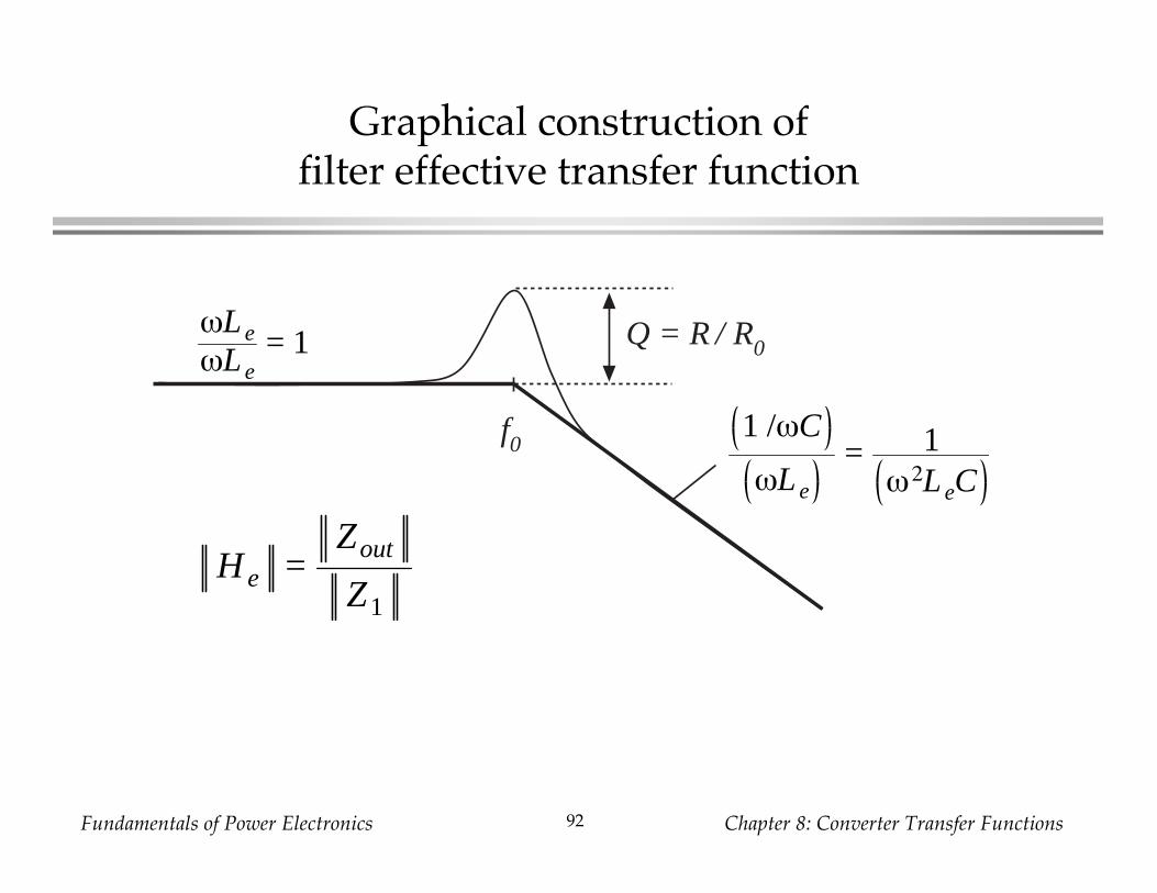
Graphical construction offilter effective transfer function
f0
Q = R / R0ωLe
ωLe= 1
1 /ωC
ωLe
= 1ω2LeC
H e =Zout
Z1

Fundamentals of Power Electronics Chapter 8: Converter Transfer Functions93
Boost and buck-boost converters: Le = L / D’ 2
1ωC
R
|| Zout ||
f0
R0
Q = R / R0
ωL
D' 2increasing
D

Fundamentals of Power Electronics Chapter 8: Converter Transfer Functions94
8.4. Measurement of ac transfer functionsand impedances
Network Analyzer
Injection source Measured inputs
vy
magnitudevz
frequencyvz
outputvz
+ –
input
vx
input+ – + –
vy
vx
vy
vx
Data
17.3 dB
– 134.7˚
Data busto computer

Fundamentals of Power Electronics Chapter 8: Converter Transfer Functions95
Swept sinusoidal measurements
• Injection source produces sinusoid of controllable amplitude andfrequency
• Signal inputs and perform function of narrowband trackingvoltmeter:
Component of input at injection source frequency is measuredNarrowband function is essential: switching harmonics and othernoise components are removed
• Network analyzer measures
vz
vx vy
∠vy
vx
vy
vx
and

Fundamentals of Power Electronics Chapter 8: Converter Transfer Functions96
Measurement of an ac transfer function
Network Analyzer
Injection source Measured inputs
vy
magnitudevz
frequencyvz
outputvz
+ –
input
vx
input+ – + –
vy
vx
vy
vx
Data
–4.7 dB
– 162.8˚
Data busto computer
Deviceunder test
G(s)
inpu
t output
VCC
DCbias
adjust
DCblocking
capacitor
• Potentiometerestablishes correctquiescent operatingpoint
• Injection sinusoidcoupled to deviceinput via dc blockingcapacitor
• Actual device inputand output voltagesare measured asand
• Dynamics of blockingcapacitor are irrelevant
vx
vy
vy(s)
vx(s)= G(s)

Fundamentals of Power Electronics Chapter 8: Converter Transfer Functions97
Measurement of an output impedance
Z(s) =v(s)i(s)
VCC
DCbias
adjust
Deviceunder test
G(s)
inpu
t output
Zout +– vz
iout
vy
+ –
voltageprobe
ZsRsource
DC blockingcapacitor
currentprobe
vx
+ –
Zout(s) =vy(s)
iout(s) amplifierac input = 0

Fundamentals of Power Electronics Chapter 8: Converter Transfer Functions98
Measurement of output impedance
• Treat output impedance as transfer function from output current tooutput voltage:
• Potentiometer at device input port establishes correct quiescentoperating point
• Current probe produces voltage proportional to current; this voltageis connected to network analyzer channel
• Network analyzer result must be multiplied by appropriate factor, toaccount for scale factors of current and voltage probes
vx
Z(s) =v(s)i(s)
Zout(s) =vy(s)
iout(s) amplifierac input = 0

Fundamentals of Power Electronics Chapter 8: Converter Transfer Functions99
Measurement of small impedances
Impedanceunder test
Z(s) +– vz
iout
vy
+
–
voltageprobe
Rsource
vx+
–
Network Analyzer
Injection source
Measuredinputs
voltageprobereturnconnection
injectionsourcereturnconnection
iout
Zrz Zprobe
k iout
(1 – k) iout
+ –(1 – k) iout Z probe
Grounding problemscause measurementto fail:Injection current canreturn to analyzer viatwo paths. Injectioncurrent which returnsvia voltage probe groundinduces voltage drop involtage probe, corrupting themeasurement. Networkanalyzer measures
Z + (1 – k) Z probe = Z + Z probe || Zrz
For an accurate measurement, requireZ >> Z probe || Zrz

Fundamentals of Power Electronics Chapter 8: Converter Transfer Functions100
Improved measurement: add isolation transformer
Impedanceunder test
Z(s) +– vz
iout
vy
+
–
voltageprobe
Rsource
vx+
–
Network Analyzer
Injection source
Measuredinputs
voltageprobereturnconnection
injectionsourcereturnconnection
Zrz Zprobe
+ –0V
0
iout
1 : n
Injectioncurrent mustnow returnentirelythroughtransformer.No additionalvoltage isinduced involtage probegroundconnection

Fundamentals of Power Electronics Chapter 8: Converter Transfer Functions101
8.5. Summary of key points
1. The magnitude Bode diagrams of functions which vary as (f / f0)nhave slopes equal to 20n dB per decade, and pass through 0dB at f = f0.
2. It is good practice to express transfer functions in normalized pole-zero form; this form directly exposes expressions for the salientfeatures of the response, i.e., the corner frequencies, referencegain, etc.
3. The right half-plane zero exhibits the magnitude response of theleft half-plane zero, but the phase response of the pole.
4. Poles and zeroes can be expressed in frequency-inverted form,when it is desirable to refer the gain to a high-frequency asymptote.
Fundamentals of Power Electronics Chapter 8: Converter Transfer Functions102
Summary of key points
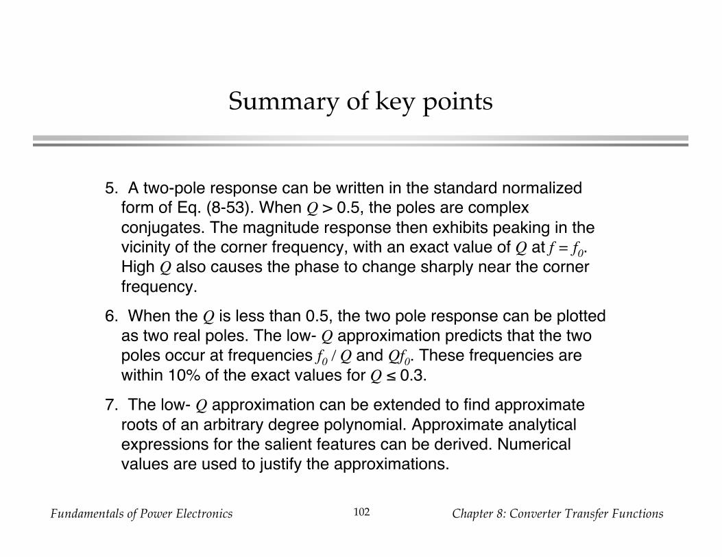
5. A two-pole response can be written in the standard normalizedform of Eq. (8-53). When Q > 0.5, the poles are complexconjugates. The magnitude response then exhibits peaking in thevicinity of the corner frequency, with an exact value of Q at f = f0.High Q also causes the phase to change sharply near the cornerfrequency.
6. When the Q is less than 0.5, the two pole response can be plottedas two real poles. The low- Q approximation predicts that the twopoles occur at frequencies f0 / Q and Qf0. These frequencies arewithin 10% of the exact values for Q ≤ 0.3.
7. The low- Q approximation can be extended to find approximateroots of an arbitrary degree polynomial. Approximate analyticalexpressions for the salient features can be derived. Numericalvalues are used to justify the approximations.

Fundamentals of Power Electronics Chapter 8: Converter Transfer Functions103
Summary of key points
8. Salient features of the transfer functions of the buck, boost, and buck-boost converters are tabulated in section 8.2.2. The line-to-outputtransfer functions of these converters contain two poles. Their control-to-output transfer functions contain two poles, and may additionallycontain a right half-pland zero.
9. Approximate magnitude asymptotes of impedances and transferfunctions can be easily derived by graphical construction. Thisapproach is a useful supplement to conventional analysis, because ityields physical insight into the circuit behavior, and because itexposes suitable approximations. Several examples, including theimpedances of basic series and parallel resonant circuits and thetransfer function He(s) of the boost and buck-boost converters, areworked in section 8.3.
10. Measurement of transfer functions and impedances using a networkanalyzer is discussed in section 8.4. Careful attention to groundconnections is important when measuring small impedances.