characterisationofhigh-frequencynoise in graphene fets at
TRANSCRIPT
Characterisation of high-frequency noisein graphene FETs at different ambienttemperaturesMaster’s thesis in Applied Physics
Junjie Li
Department of Microtechnology and NanoscienceCHALMERS UNIVERSITY OF TECHNOLOGYGothenburg, Sweden 2019

Master’s thesis 2019
Characterisation of high-frequencynoise in graphene FETs at
different ambient temperatures
Junjie Li
Terahertz and Millimetre Wave LaboratoryDepartment of Microtechnology and Nanoscience
Chalmers University of TechnologyGothenburg, Sweden 2019
Characterisation of high-frequency noise in graphene FETs at different ambient tem-peratures
© Junjie Li, 2019.
Supervisor: Xinxin Yang, Department of Microtechnology and NanoscienceExaminer: Jan Stake, Department of Microtechnology and Nanoscience
Master’s Thesis 2019Terahertz and Millimetre Wave LaboratoryDepartment of Microtechnology and NanoscienceChalmers University of TechnologySE-412 96 Gothenburg, SwedenTelephone +46 31 772 1000
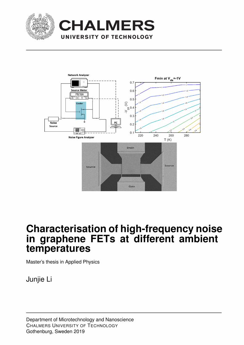
Cover:Top left: Schematic block diagram of thermal noise measurement setup for 50 Ωtermination method.Top right: Fmin in decibel versus temperature at 6.5 GHz and drain bias of -1 VBottom: SEM image of a GFET
Typeset in LATEXGothenburg, Sweden 2019
iv

Characterisation of high-frequency noise in graphene FETs at different ambient tem-peraturesJunjie LiTerahertz and Millimetre Wave LaboratoryDepartment of Microtechnology and NanoscienceChalmers University of Technology
AbstractGraphene is a promising channel material for high-frequency field-effect transistors,owing to its intrinsically high carrier velocity and purely two-dimensional structure.At high frequencies, the noise originated in device itself, especially the thermalnoise, becomes very crucial for the performance of transistors. The thermal noisecan be influenced by ambient temperature or self-heating due to high drain bias.This motivates the study of the effect of temperature on the noise performance ofgraphene field-effect transistors (GFETs).
In this thesis, the results on high-frequency noise characterisation and modellingof the GFETs at different temperature and bias conditions are presented. The basicidea and main procedures of high-frequency noise modelling are based on Pospieszal-ski’s noise model. Two different high-frequency noise characterisation techniques,i.e., the Y-factor and cold-source methods, and two calculation methods of high-frequency noise parameters, i.e., the source-pull and 50 Ω impedance termination(F50) methods, have been analysed and discussed. The high-frequency noise of theGFETs at an ambient temperature range from -60 C to 25 C is presented. Theminimum noise figure (Fmin) of the GFETs decreases with the drain bias and satu-rates above approximately -1 V due to the carrier mobility saturation in the channel.The noise performance shows a rather strong dependence on both temperature andgate bias mainly due to the change of carrier density and the contact resistance. Theminimum noise figure (Fmin) is 1.2 dB at 6.5 GHz at room temperature, which iscomparable with that of the best metal-semiconductor field effect transistors. Andit decreases down to 0.3 dB at 8 GHz for an ambient temperature of -60 C. Anempirical noise model for the GFETs considering both temperature and gate voltagehas been proposed and verified by the experimental results.
In conclusion, a way to characterise the temperature dependence of noise perfor-mance of the GFETs is discussed, which allows for further development of low-noiseGFETs for high-frequency applications.
Keywords: graphene, GFET, noise characterisation, thermal experiments, minimumnoise figure, F50 method, field effect transistors, microwave electronics
v


AcknowledgementsFirst, I would like to give my greatest gratitude to my supervisor Ms. Xinxin Yangwho gave me a lot of assistance and instruction in this work and she also encouragedme whenever I had problems with it. She is always very patient to read the thesisand paper and give me advise for many times.
I would also like to thank Dr. Andrei Vorobiev who is always willing to discussand give me suggestions helpfully. And I would like to thank Prof. Jan Stake whoprovides me with this great opportunity to working in the TML. And I also wantto say thanks to Ms. Marlene Bonmann and Mr. Muhammad Asad for the helpof the fabrication of the device. And I also want to thank Ms. Eunjung Cha forproviding her device for measuring and comparing. And I would thank Prof. SergueiCherednichenko for the advice and the help of the measurement equipment. And Iwant to show my respect to Dr. Michael Andersson who gives many useful adviceand documents for the measurement.
Finally, I would like to thank my family and friends for supporting me all thetime.
Junjie Li, Gothenburg, August 2019
vii


Contents
List of figures xi
List of tables xiii
List of abbreviations xv
List of notations xvii
1 Introduction 11.1 Thesis outline . . . . . . . . . . . . . . . . . . . . . . . . . . . . . . . 2
2 Theoretical background 52.1 Noise theory . . . . . . . . . . . . . . . . . . . . . . . . . . . . . . . . 5
2.1.1 Noise . . . . . . . . . . . . . . . . . . . . . . . . . . . . . . . . 52.1.2 Noise parameters . . . . . . . . . . . . . . . . . . . . . . . . . 62.1.3 Pospieszalski’s noise model . . . . . . . . . . . . . . . . . . . . 7
2.2 High-frequency noise characterization techniques . . . . . . . . . . . . 92.2.1 Y-factor method . . . . . . . . . . . . . . . . . . . . . . . . . 92.2.2 Cold-source method . . . . . . . . . . . . . . . . . . . . . . . . 10
2.3 Fmin calculation methods . . . . . . . . . . . . . . . . . . . . . . . . . 112.3.1 Source-pull method . . . . . . . . . . . . . . . . . . . . . . . . 112.3.2 50 Ω termination method . . . . . . . . . . . . . . . . . . . . 122.3.3 Comparison and analysis . . . . . . . . . . . . . . . . . . . . . 13
3 Fabrication and characterisation of GFETs 153.1 GFET design and fabrication . . . . . . . . . . . . . . . . . . . . . . 153.2 DC characteristics . . . . . . . . . . . . . . . . . . . . . . . . . . . . . 163.3 S-parameters . . . . . . . . . . . . . . . . . . . . . . . . . . . . . . . 183.4 Noise characterisation . . . . . . . . . . . . . . . . . . . . . . . . . . 20
3.4.1 Measurement setups . . . . . . . . . . . . . . . . . . . . . . . 203.4.2 Fmin at different temperatures and bias voltages . . . . . . . . 233.4.3 Empirical noise model for GFETs . . . . . . . . . . . . . . . . 27
4 Conclusion & future work 294.1 Summary . . . . . . . . . . . . . . . . . . . . . . . . . . . . . . . . . 294.2 Outlook . . . . . . . . . . . . . . . . . . . . . . . . . . . . . . . . . . 29
ix

Contents
A Matlab code IA.1 Main file . . . . . . . . . . . . . . . . . . . . . . . . . . . . . . . . . . I
B Conference paper V
x

List of Figures
1.1 State-of-the-art intrinsic (a) fT and (b) fmax for HEMTs, Si CMOSs,CNT and NW FETs against reported GFETs [14,15]. . . . . . . . . 2
1.2 Fmin for HEMTs, Si CMOS, MESFET and against reported intrinsicGFETs [18,20,21,22,23]. . . . . . . . . . . . . . . . . . . . . . . . . . 3
2.1 A block diagram of a microwave amplifier [24]. . . . . . . . . . . . . . 52.2 (a) Equivalent circuit with the outside noise current sources i1 and i2
respectively. (b) Equivalent circuit with noise voltage source e andnoise current source i at the input [33,34]. . . . . . . . . . . . . . . . 8
2.3 Equivalent circuit and the noise model of GFETs [36]. . . . . . . . . . 82.4 The output noise power versus source temperature of linear, two-port
devices [30]. . . . . . . . . . . . . . . . . . . . . . . . . . . . . . . . . 92.5 Circles of a series of constant noise figure [39]. . . . . . . . . . . . . . 122.6 Comparison of the measured four noise parameters versus frequency.
Solid line: conventional technique by using source-pull. Dashed line:50Ω termination method [41]. . . . . . . . . . . . . . . . . . . . . . . 14
3.1 (a) Side view of the GFET. (b) Layout of the GFET. . . . . . . . . . 153.2 SEM image of a two-finger GFET with gate length Lg = 0.75 µm and
gate width Wg = 2× 15 µm. The inset shows a 70 tilted view of thegate area [49]. . . . . . . . . . . . . . . . . . . . . . . . . . . . . . . . 16
3.3 Transfer curve at drain voltage of 0.1 V and temperatures rangingfrom -60 C to 25 C for (a) device A and (b) device B. . . . . . . . . 17
3.4 Fitting of the transfer curve of device A at 25 C . . . . . . . . . . . . 173.5 Output curve of device A at gate voltage from -1.2 V to 0.6 V in steps
of 0.2 V (a) at 213 K and 300 K, respectively, and (b) at 4 K and 300K, respectively. . . . . . . . . . . . . . . . . . . . . . . . . . . . . . . 18
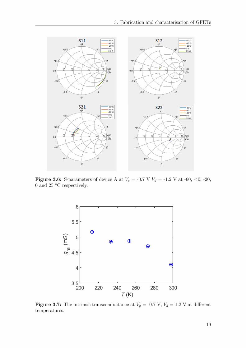
3.6 S-parameters of device A at Vg = -0.7 V Vd = -1.2 V at -60, -40, -20,0 and 25 C respectively. . . . . . . . . . . . . . . . . . . . . . . . . . 19
3.7 The intrinsic transconductance at Vg = -0.7 V, Vd = 1.2 V at differenttemperatures. . . . . . . . . . . . . . . . . . . . . . . . . . . . . . . . 19
3.8 The source-pull noise measurement setup. . . . . . . . . . . . . . . . 203.9 Schematic of source-pull noise measurement setup. . . . . . . . . . . . 213.10 Schematic block diagram of noise measurement setup for 50 Ω termi-
nation method. . . . . . . . . . . . . . . . . . . . . . . . . . . . . . . 22
xi
List of Figures
3.11 (a) Tmin and Td calculated from 50 Ohm impedance with the datafrom the previous paper. (b) Fmin comparison between source-pullmethod and 50 Ohm method. . . . . . . . . . . . . . . . . . . . . . . 22
3.12 (a) Fmin versus frequency of device A at different temperatures (-60C, -40 C, -20 C, 0 C and 25 C) with gate voltage of -0.1 V anddrain voltage of -1.4 V. (b) Fmin versus temperature of device A fordifferent frequencies (12, 14, 16, and 18 GHz) at gate voltage of -0.1V and drain voltage of -1.4V. . . . . . . . . . . . . . . . . . . . . . . 23
3.13 Fmin in decibel of device A versus temperature at 6.5 GHz and drainbias of -0.8, -1, -1.2, -1.4 V respectively . . . . . . . . . . . . . . . . . 24
3.14 Fmin in decibel of device A versus drain bias at 6.5 GHz and -60, -20,0, and 25 C respectively . . . . . . . . . . . . . . . . . . . . . . . . . 24
3.15 Fmin versus frequency of device B at different drain voltages (-0.4,-0.6, -0.8, -1.2 and -1.4 V), gate voltage of 0.5 V at (a) -60 C and(b) 25 C. . . . . . . . . . . . . . . . . . . . . . . . . . . . . . . . . . 25
3.16 Fmin versus frequency of device B at different temperatures (-60 C,-45 C, -25 C and 25 C), gate voltage of 0.5 V and drain voltage of-1.4 V. . . . . . . . . . . . . . . . . . . . . . . . . . . . . . . . . . . . 25
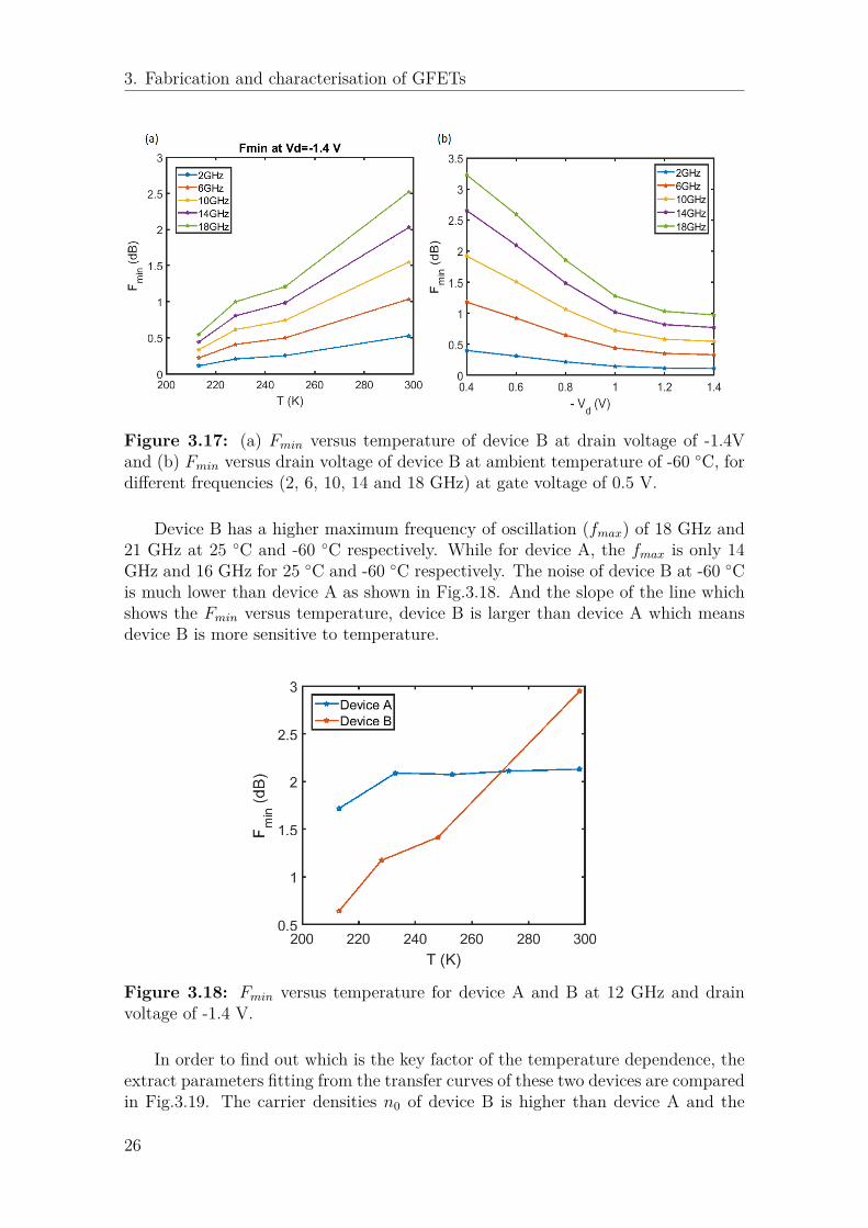
3.17 (a) Fmin versus temperature of device B at drain voltage of -1.4V and(b) Fmin versus drain voltage of device B at ambient temperature of-60 C, for different frequencies (2, 6, 10, 14 and 18 GHz) at gatevoltage of 0.5 V. . . . . . . . . . . . . . . . . . . . . . . . . . . . . . . 26
3.18 Fmin versus temperature for device A and B at 12 GHz and drainvoltage of -1.4 V. . . . . . . . . . . . . . . . . . . . . . . . . . . . . . 26
3.19 (a) The carrier densities n0, (b) the carrier mobility µ, (c) the contactresistances R versus temperature are fitting from the transfer curvesof device A and device B, respectively . . . . . . . . . . . . . . . . . . 27
3.20 Modelled (line) and measured (circle) noise parameters for GFETwith Vds = 1.2 V (a) at frequency of 6.5 GHz and (b) Vgs at -0.1 Vwith temperature of -60 C (blue), -20 C (black) and 25 C (red),respectively. . . . . . . . . . . . . . . . . . . . . . . . . . . . . . . . . 28
xii
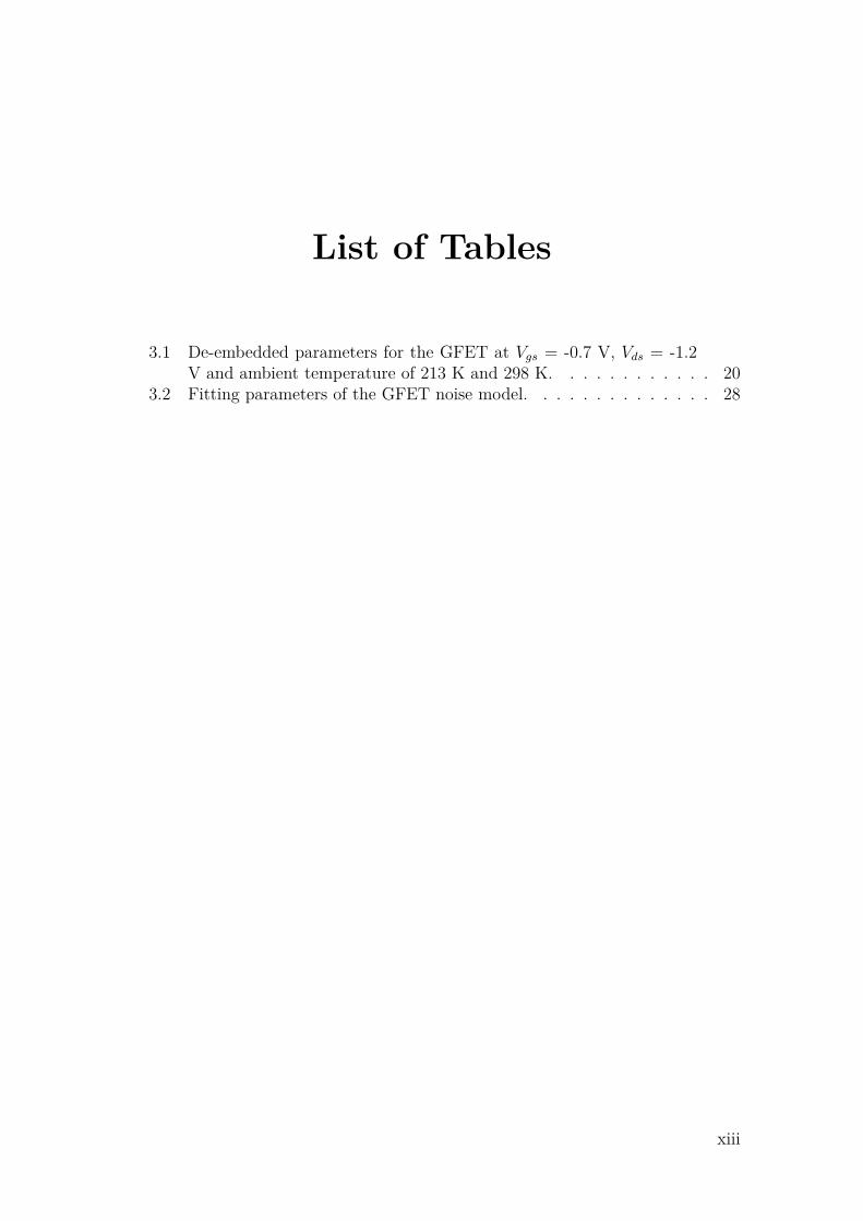
List of Tables
3.1 De-embedded parameters for the GFET at Vgs = -0.7 V, Vds = -1.2V and ambient temperature of 213 K and 298 K. . . . . . . . . . . . 20
3.2 Fitting parameters of the GFET noise model. . . . . . . . . . . . . . 28
xiii

List of Tables
xiv

List of Abbreviations
Al aluminiumAl2O3 aluminium oxideCMOS complementary metal-oxide-semiconductorCVD chemical vapour depositionDUT device-under-testENR excess noise ratioFET field effect transistorGaAs gallium arsenideGFET graphene field effect transistorhBN hexagonal boron nitrideHEMT high electron mobility transistorInP indium phosphideLNA low noise amplifierMESFET metal-semiconductor field effect transistorMOSFET metal oxide semiconductor field effect transistorSiC silicon carbideSiO2 silicon oxideSNR signal-to-noise power ratioRF radio frequencyTHz terahertz
xv

0. List of Abbreviations
xvi

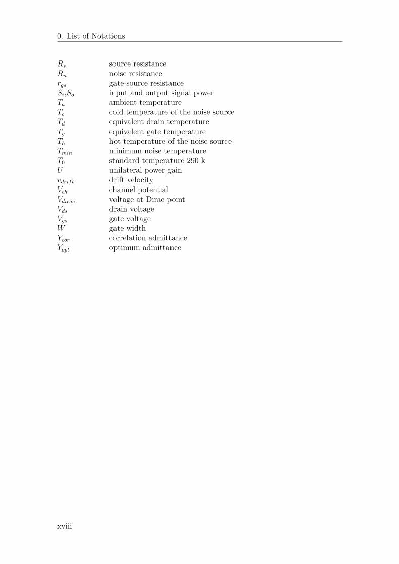
List of Notations
Γs source reflection coefficientΓL load reflection coefficientΓopt source reflection coefficient for minimum noiseµ carrier mobilityω angular frequencya lattice constantB noise bandwidthCds stray capacitance between electrodesCg gate capacitanceCgd gate-drain capacitanceCgs gate-source capacitanceCpg gate pad capacitanceCpd drain pad capacitanceF noise factorF50 noise figure with 50 Ω terminationFmin minimum noise figurefT transit frequencyfmax maximum frequency of oscillationG gainGav available gaingds drain conductancegm transconductanceh21 short circuit current gainId drain currentkB Boltzmann’s constantL gate lengthM noise measuren charge carrier concentrationn0 residual charge carrier concentrationNa component added noise powerNc cold-source noise powerNh hot-source noise powerNi,No input and output noise powerNF noise figureRc metal-graphene contact resistanceRd drain resistanceRg gate resistance
xvii
0. List of Notations
Rs source resistanceRn noise resistancergs gate-source resistanceSi,So input and output signal powerTa ambient temperatureTc cold temperature of the noise sourceTd equivalent drain temperatureTg equivalent gate temperatureTh hot temperature of the noise sourceTmin minimum noise temperatureT0 standard temperature 290 kU unilateral power gainvdrift drift velocityVch channel potentialVdirac voltage at Dirac pointVds drain voltageVgs gate voltageW gate widthYcor correlation admittanceYopt optimum admittance
xviii
1Introduction
High-frequencies electronics working at microwaves (0.3 - 100 GHz) and terahertzwaves (loosely defined as 0.1 - 10 THz) have attracted a large number of interests be-cause of their existing and potential applications. Nowadays, microwave electronicshave been extensively used for wireless communication from mobile phones to satel-lites. Over the past few decades, the terahertz part of the electromagnetic spectrumhas also been studied to a large extent. The larger bandwidth and lower energy ofterahertz waves can make it be used in medicine and disease diagnostics [1], securityinspection [2] and high-speed communication [3]. Most of these applications relyon the development of high-frequency field-effect transistors (FETs) and integratedcircuits.
The FET is a three-terminal device where the current that flows through canbe controlled by an electric field applied at the gate. The first FET was invented byWilliam Shockley, John Bardeen and Walter Brattain in 1952 [4]. The traditionalFETs are made of Si and GaAs which have been widely used as digital logic devicesand radio-frequency devices. However, the operating frequency of traditional FETsis less than 50 GHz due to the limitation of the structure and material. Thereare two ways to increase the operating frequency of the FETs: either to improvethe structure or introduce new material with better properties. The high electronmobility transistor (HEMT) invented by T. Mimura in 1979 utilises GaAs and Al-GaAs heterostructer to form a two-dimensional electron gas channel [5]. And thenInxGa1−xAs was introduced to increase the mobility which shows a very high maxi-mum frequency of oscillation fmax up to 1.2 THz [6].
However, for even higher frequencies, the new material with higher electronmobility such as the two-dimensional semi-metal material, graphene, was introducedby Novoselov et.al in 2004 [7]. Since then it has raised a lot of interest in fundamentalresearches as well as applications. Graphene has only one layer of carbon in ahexagonal honeycomb lattice with a carbon-carbon bond length of 1.42 Å and thelattice constant of a = 2.476 Å. Unlike the conventional semiconductor materialwhich has a bandgap between the valence band and conduction band, there aresix points in momentum space of graphene that has no bandgap. Around thesepoints, the dispersion relation of graphene is approximately linear and these pointsare named Dirac point. The unique structure of graphene gives it a remarkableelectron mobility at room temperature, more than 2×105 cm2/Vs with a suspendedmonolayer in vacuum [8]. These properties make it a very suitable channel materialfor high-frequency FETs. The first top-gated graphene field-effect transistor (GFET)was investigated in 2007 [9]. Also, the atomic thickness of graphene allows GFETsto be scaled to shorter channel lengths and higher speeds without encountering
1
1. Introduction
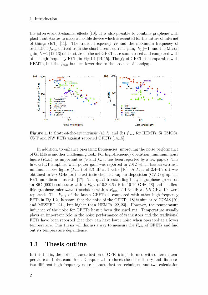
the adverse short-channel effects [10]. It is also possible to combine graphene withplastic substrates to make a flexible device which is essential for the future of internetof things (IoT) [11]. The transit frequency fT and the maximum frequency ofoscillation fmax derived from the short-circuit current gain, |h21|=1, and the Masongain, U=1 [12,13] of the state-of-the-art GFETs are summarised and compared withother high frequency FETs in Fig.1.1 [14,15]. The fT of GFETs is comparable withHEMTs, but the fmax is much lower due to the absence of bandgap.
Figure 1.1: State-of-the-art intrinsic (a) fT and (b) fmax for HEMTs, Si CMOSs,CNT and NW FETs against reported GFETs [14,15].
In addition, to enhance operating frequencies, improving the noise performanceof GFETs is another challenging task. For high-frequency operation, minimum noisefigure (Fmin), as important as fT and fmax, has been reported by a few papers. Thefirst GFET amplifier with power gain was reported in 2012 which has an extrinsicminimum noise figure (Fmin) of 3.3 dB at 1 GHz [16]. A Fmin of 2.4–4.9 dB wasobtained in 2–8 GHz for the extrinsic chemical vapour deposition (CVD) grapheneFET on silicon substrate [17]. The quasi-freestanding bilayer graphene grown onan SiC (0001) substrate with a Fmin of 0.8-3.6 dB in 10-26 GHz [18] and the flex-ible graphene microwave transistors with a Fmin of 1.34 dB at 5.5 GHz [19] werereported. The Fmin of the latest GFETs is compared with other high-frequencyFETs in Fig.1.2. It shows that the noise of the GFETs [18] is similar to COMS [20]and MESFET [21], but higher than HEMTs [22, 23]. However, the temperatureinfluence of the noise for GFETs hasn’t been discussed yet. Temperature usuallyplays an important role in the noise performance of transistors and the traditionalFETs have been reported that they can have lower noise when operated at a lowertemperature. This thesis will discuss a way to measure the Fmin of GFETs and findout its temperature dependence.
1.1 Thesis outlineIn this thesis, the noise characterisation of GFETs is performed with different tem-perature and bias conditions. Chapter 2 introduces the noise theory and discussestwo different high-frequency noise characterisation techniques and two calculation
2

1. Introduction
Figure 1.2: Fmin for HEMTs, Si CMOS, MESFET and against reported intrinsicGFETs [18,20,21,22,23].
methods of high-frequency noise parameters. Chapter 3 shows the fabrication pro-cess, experimental results and noise modelling of the GFETs. Chapter 4 concludesthe work results and depicts the possible future work.
3
1. Introduction
4
2Theoretical background
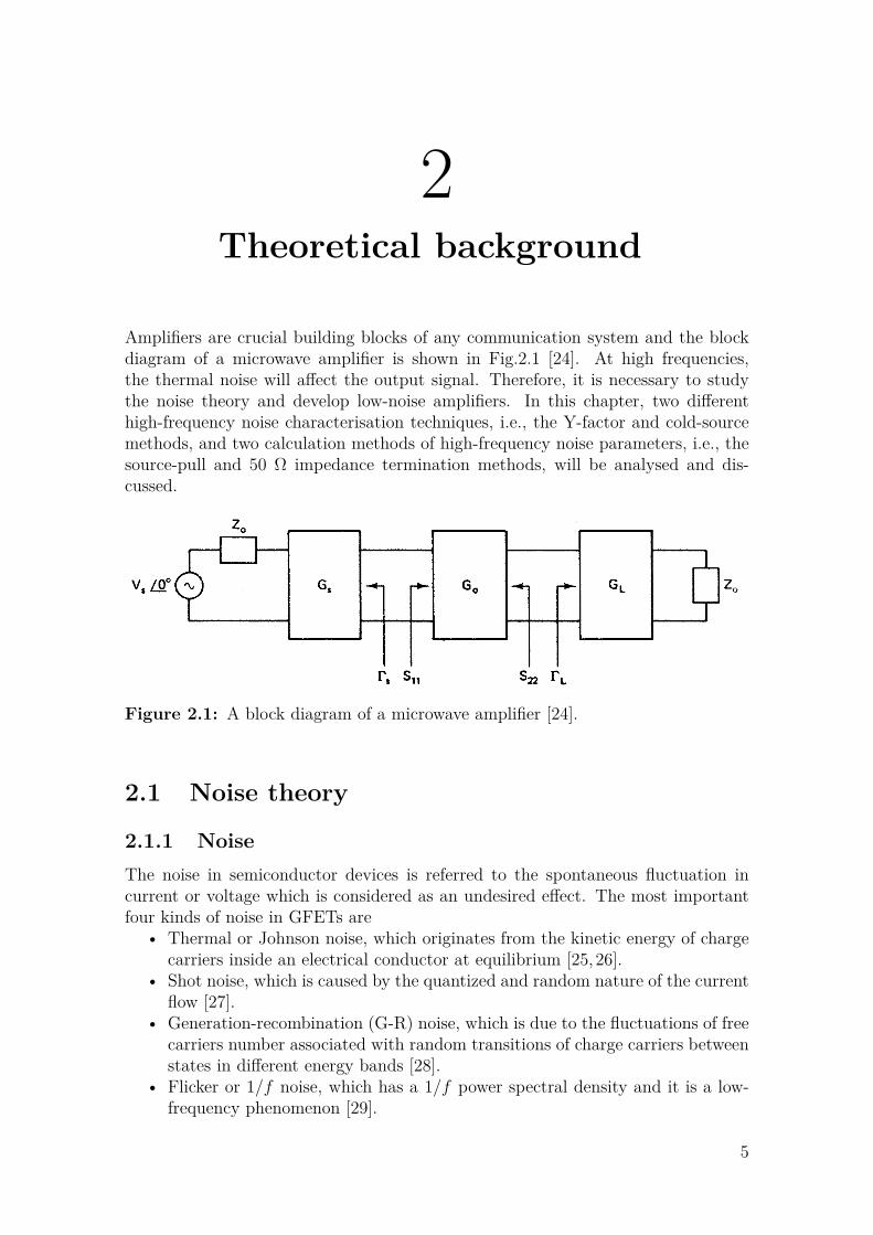
Amplifiers are crucial building blocks of any communication system and the blockdiagram of a microwave amplifier is shown in Fig.2.1 [24]. At high frequencies,the thermal noise will affect the output signal. Therefore, it is necessary to studythe noise theory and develop low-noise amplifiers. In this chapter, two differenthigh-frequency noise characterisation techniques, i.e., the Y-factor and cold-sourcemethods, and two calculation methods of high-frequency noise parameters, i.e., thesource-pull and 50 Ω impedance termination methods, will be analysed and dis-cussed.
Figure 2.1: A block diagram of a microwave amplifier [24].
2.1 Noise theory
2.1.1 NoiseThe noise in semiconductor devices is referred to the spontaneous fluctuation incurrent or voltage which is considered as an undesired effect. The most importantfour kinds of noise in GFETs are
• Thermal or Johnson noise, which originates from the kinetic energy of chargecarriers inside an electrical conductor at equilibrium [25,26].
• Shot noise, which is caused by the quantized and random nature of the currentflow [27].
• Generation-recombination (G-R) noise, which is due to the fluctuations of freecarriers number associated with random transitions of charge carriers betweenstates in different energy bands [28].
• Flicker or 1/f noise, which has a 1/f power spectral density and it is a low-frequency phenomenon [29].
5

2. Theoretical background
The G-R noise is lower than gigahertz [28] and the shot noise and flicker noisebecome important only when FETs have a large gate leakage current [29]. Therefore,this thesis will only investigate the thermal noise for high-frequency devices.
2.1.2 Noise parametersTo characterise the noise for high-frequency FETs, a figure of merit is required todescribe the performance of it.
The highest output signal-to-noise power ratio (SNR) of a system equals tothe input SNR when all the components in the system is noiseless. But usually,the components which refers to FETs here have their own noise that decreases theoutput SNR. So the ratio of the signal-to-noise power ratio at the input to the signal-to-noise power ratio at the output, defined as the noise factor (F ), can describe thenoise performance of a FET [30]:
F = Si/Ni
So/No
, (2.1)
where Si and So are the input and output signal power, Ni and No are the inputand output noise power, respectively.
F is a figure-of-merit that describes the degradation of SNR due to the noisecaused by the components in a signal chain. Take the amplifier as an example, if theamplifier is noiseless, then the output signal is simply the input multiplied by theamplifier gain. But realistically, the amplifier also has noise and the output signalis larger than the input signal multiplied by the gain. So F can be expressed as
F = Si/Ni
GSi/ (Na +GNi)= Na +GNi
GNi
, (2.2)
where Na is the noise added by the amplifier, G is the gain of the amplifier.Asystem amplifies signal and noise at the same time which does not change the SNR.Therefore, SNR is only dependent on the temperature of the noise source, whichmeans the F should not be related to the gain.
F is a property of a device-under-test (DUT) which is not dependent on the in-put signal. The F of a DUT is influenced by the impedance mismatch between thenoise source and DUT, and the impedance match between DUT and the measuringinstrument. Therefore, a special tuner is needed to provide a certain source reflec-tion coefficient to make a perfectly matched system. The F depending on sourceimpedance presented by the tuner is described by as
F = Fmin + 4Rn
Zc
|Γopt − Γs|2
|1 + Γopt|2(1− |Γs|2
) , (2.3)
where Fmin is the minimum noise factor and Rn is the noise resistance. Γ is thesource reflection coefficient. Only when Γs = Γ opt , the F of the system equalsF min . Fmin, Rn and Γ opt are usually frequency dependent.
The DUT cannot be measured individually. Usually, it is measured in a system.To find the F of the component that is interested, the F of the overall system and
6

2. Theoretical background
the gain of other components are needed. Then the F of the device can be calculatedfrom the overall noise figure:
Fsys = F1 + F2 − 1G1
. (2.4)
The noise measure (M) is another important parameter for a system whenconsidering cascaded two-ports [31] and it is defined as
M = F − 11− 1
Ga
, (2.5)
where Ga is the available power gain and the M is a function of source admittance.For high-frequency FETs, thermal noise is the most important noise source.
Because the thermal noise of an electric system usually comes from the vibration ofcarriers, including electrons and holes. And the vibrations spectral is nearly uniformover RF and microwave frequencies, which is the signal spectral that is interested.So it will contribute to the signal-to-noise power ratio (SNR). The noise power of athermal source at temperature T is N = kBTB, where kB is Boltzmann’s constant(1.38× 10⁻²³ J/ K) , and B is the system’s noise bandwidth. The IRE (forerunnerof the IEEE) adopted 290 K as the standard temperature T0 for thermal source atthe input. Then the F becomes
F = TaT0
+ 1. (2.6)
where Ta is the noise temperature of the DUT.F in Eq. (2.1-2.6) is often called noise factor or sometimes noise figure in linear
terms. Noise figure usually is F expressed in log scale:
NF = 10 log10 F. (2.7)
2.1.3 Pospieszalski’s noise modelIn high-frequency FETs, the thermal noise comes from the resistive parts of thechannel, parasitic resistances and high-field diffusion noise from the velocity sat-urated part of the channel [32]. The intrinsic FET can be considered as a lineartwo-port system as the equivalent circuit using different matrix representations as inFig.2.2 [33, 34]. Fig.2.2a shows an equivalent circuit with two noise current sourcesi1 and i2 with an inner infinite impedance represented by admittance matrix (Y).It can also present all the internal noise sources only at the input side by a noisecurrent source i and a noise voltage source e represented by chain matrix (ABCD)as shown in Fig.2.2b.
In the equivalent circuit of GFETs, the noise can be expressed as drain and gatecurrent sources, id and ig. In Pospieszalski’s noise model, the resistive elements of theintrinsic circuit are assigned to the unrelated equivalent gate and drain temperatureTg and Td:
i2g = 4kB∆fTg/rgs, (2.8)
7
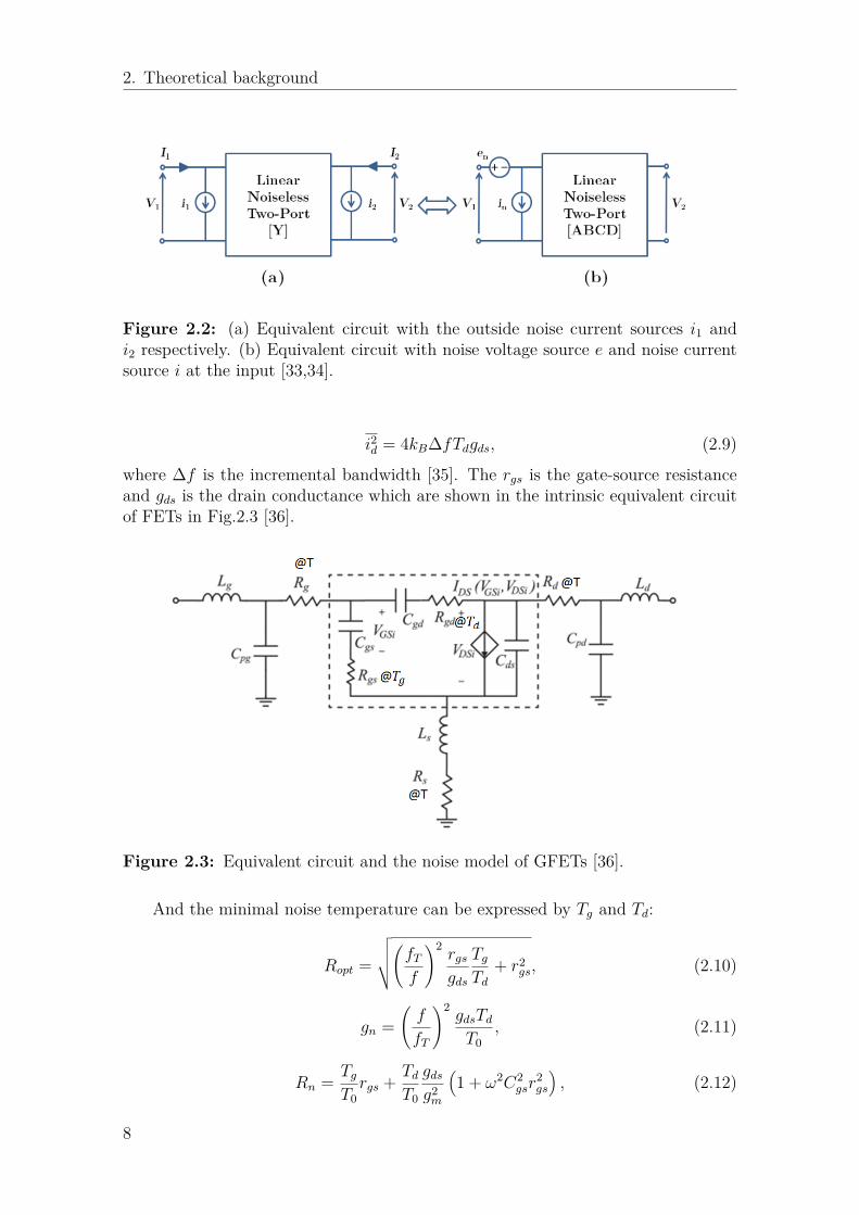
2. Theoretical background
Figure 2.2: (a) Equivalent circuit with the outside noise current sources i1 andi2 respectively. (b) Equivalent circuit with noise voltage source e and noise currentsource i at the input [33,34].
i2d = 4kB∆fTdgds, (2.9)
where ∆f is the incremental bandwidth [35]. The rgs is the gate-source resistanceand gds is the drain conductance which are shown in the intrinsic equivalent circuitof FETs in Fig.2.3 [36].
Figure 2.3: Equivalent circuit and the noise model of GFETs [36].
And the minimal noise temperature can be expressed by Tg and Td:
Ropt =
√√√√(fTf
)2rgsgds
TgTd
+ r2gs, (2.10)
gn =(f
fT
)2gdsTdT0
, (2.11)
Rn = TgT0rgs + Td
T0
gdsg2m
(1 + ω2C2
gsr2gs
), (2.12)
8
2. Theoretical background
Tmin = 2 ffT
√√√√gdsrgsTgTd +(f
fT
)2
r2gsg
2dsT
2d + 2
(f
fT
)2
rgsgdsTd, (2.13)
where gm is the transconductance, ω is the frequency, Cgs is gate-source capacitanceand fT is cut-off frequency. The relationship between Fmin and Tmin is
Fmin = TminT0
+ 1. (2.14)
2.2 High-frequency noise characterization techniques
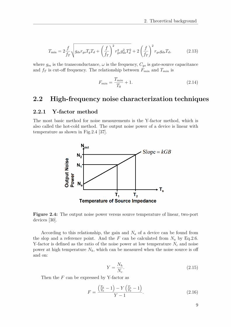
2.2.1 Y-factor methodThe most basic method for noise measurements is the Y-factor method, which isalso called the hot-cold method. The output noise power of a device is linear withtemperature as shown in Fig.2.4 [37].
Figure 2.4: The output noise power versus source temperature of linear, two-portdevices [30].
According to this relationship, the gain and Na of a device can be found fromthe slop and a reference point. And the F can be calculated from Na by Eq.2.6.Y-factor is defined as the ratio of the noise power at low temperature Nc and noisepower at high temperature Nh, which can be measured when the noise source is offand on:
Y = Nh
Nc
. (2.15)
Then the F can be expressed by Y-factor as
F =
(Th
T0− 1
)− Y
(Tc
T0− 1
)Y − 1 . (2.16)
9

2. Theoretical background
Assuming that the cold temperature Tc is equal to the reference temperatureT0 = 290K. And the excess noise ratio (ENR) of a noise source is defined by
ENR = (Th − T0)T0
, (2.17)
which is usually given by the manufacturer. Now the F can be obtained from onlya Y factor:
FY = ENR
Y − 1 . (2.18)
2.2.2 Cold-source methodThe Y-factor method is convenient, but it is difficult to measure the low gain orlossy devices since the difference in noise between the hot and cold states of thenoise source is reduced to a very small amount by the attenuator. Another methodcalled the cold-source method is valid to measure the noise figure of an attenuatoror mismatched devices [37]. Because the cold-source technique computes the noisefigure only from a single noise measurement Nc which means that a better termina-tion can be used at room temperature. The F calculated by the cold-source methodis expressed by
FCS1 = Nc
T0kBBGrecGav (Γsc). (2.19)
where kBGrec is the gain-bandwidth product of the receiver, Gaν (Γsc) is the availablegain of the DUT. The room temperature is assumed to be equal to the referencetemperature T0 again [38].
In order to obtain an absolute noise power, the receiver power calibration isneeded which includes the use of a calibrated hot noise source during the calibrationstep. And after considering the second stage correction, the cold-source noise figurebecomes
FCS2 = Nc −Nc−rec
T0kBBGrecGav (Γsc)MM (Γou)+ 1Gav (Γsc)
. (2.20)
where MM is a mismatch term between the noise source and can be calculated fromS-parameter as
MM(Γ) = 1− |Γ|2∣∣∣1− s11−recΓ∣∣∣2 . (2.21)
And the factor kBGrec is given by
kBBGrec = Nh−rec −Nc−rec
Th − T0. (2.22)
where Nc−rec and Nh−rec is the output noise power measured with only the receiverafter the noise source at cold and hot temperature respectively. Th is the hot tem-perature of the noise source calculated from its ENR.
10

2. Theoretical background
2.3 Fmin calculation methods
Generally, it is not possible to obtain both minimum noise and maximum gain foran amplifier. The minimum noise figure is a trade-off between noise figure and gain.Here we present two different ways to calculate the minimum noise figure from themeasured noise figure.
2.3.1 Source-pull method
According to Eq.2.3, F varies with different source reflection coefficient Γs andFmin occurs when Γs = Γopt. The source-pull method is a way to vary the sourceimpedance in front of a DUT while measuring the noise performance of the DUT.There are four unknown parameters in the equations. Therefore, at least four mea-sured noise figures are needed for least-square fitting in order to find out the Fmin.In most cases, a tuner is used to provide different source reflection coefficients.
If x and y are set to be
x = |ΓS − Γopt|2(1− |ΓS|2
)|1 + Γopt|2
, (2.23)
y = F = Fmin + 4Rn
Z0x, (2.24)
then the F is linear with x. So by least-square fitting with each impedance andnoise figure, the Fmin can be found.
Fmin can also be found from the circles of constant noise figure. The noise figureparameter N is defined as [39]
N = |ΓS − Γopt|2
1− |ΓS|2= F − Fmin
4RN/Z0|1 + Γopt|2 . (2.25)
A fixed noise figure can be shown as a circle in the Smith plane [31]. The centreand radius of the circle of constant noise figure can be calculated as
CF = ΓoptN + 1 , (2.26)
RF =
√N(N + 1− |Γopt|2
)N + 1 . (2.27)
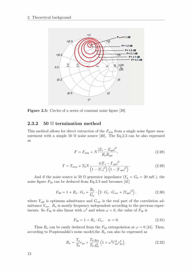
The circles for all impedance can be plotted on one Smith plane. And the point ofthe Γopt and the Fmin can be found when all the circles shrinks to a point as shownon the Fig.2.5.
11
2. Theoretical background
Figure 2.5: Circles of a series of constant noise figure [39].
2.3.2 50 Ω termination methodThis method allows for direct extraction of the Fmin from a single noise figure mea-surement with a simple 50 Ω noise source [40]. The Eq.2.3 can be also expressedas
F = Fmin +N|Zs − Zopt|2
RsRopt
, (2.28)
T = Tmin + T0N4 |Γs − Γopt|2(
1− |Γs|2) (
1− |Γopt|2) . (2.29)
And if the noise source is 50 Ω generator impedance (Yg = G0 = 20 mS ), thenoise figure F50 can be deduced from Eq.2.3 and becomes [41]
F50 = 1 +Rn ·Go + Rn
Go
·(2 ·Go ·Gcor + |Yopt|2
). (2.30)
where Yopt is optimum admittance and Gcor is the real part of the correlation ad-mittance Ycor. Rn is mostly frequency independent according to the previous exper-iments. So F50 is also linear with ω2 and when ω = 0, the value of F50 is
F50 = 1 +Rn ·Go, w = 0. (2.31)
Thus Rn can be easily deduced from the F50 extrapolation at ω = 0 [41]. Then,according to Pospieszalski’s noise model,the Rn can also be expressed as
Rn = TgT0rgs + Td
T0
gdsg2m
(1 + ω2C2
gsr2gs
). (2.32)
12

2. Theoretical background
Assume that the gate temperature Tg is simply equal to the ambient temperatureTa [40, 42]. And the Td can be derived to be
Td = Rn −Ri
1 + ω2C2gsR
2i
T0g2m
gds, Tg = T0, rgs = Ri. (2.33)
All the intrinsic parameters can be extracted from the small-signal equivalentcircuit of GFETs shown in Fig.2.3. Together with its S-parameters, the parameterscan be obtained through the following expressions [43,44]:
Cgd = − lm (Y12)ω
, (2.34)
Cgs = Im (Y11)− ωCgdω
(1 + (Re (Y11))2
(Im (Y11)− ωCed)2
), (2.35)
Ri = Re (Y11)(Im (Y11)− ωCgd)2 + (Re (Y11))2 , (2.36)
gm =√(
(Re (Y21))2 + (Im (Y21) + ωCgd)2) (
1 + ω2C2gsR
2i
), (2.37)
τ = 1ω
arcsin(−ωCgd − Im (Y21)− ωCgsRi Re (Y21)
gm
), (2.38)
Cds = Im (Y22)− ωCgdω
, (2.39)
gds = Re (Y22.) (2.40)
The Td versus frequency can be obtained by solving Eq.2.31, Eq.2.32 and Eq.2.33together. And the corresponding Ropt and Tmin can be derived to be
Ropt =r2
gs +(gmωcgs
)2TgrgsTdgds
12
, xopt = 1ωcgs
, (2.41)
Tmin = 2(ωcgsgm
)2
(Tdgds) (rgs +Ropt) . (2.42)
Then the Fmin can be calculated by using Eq.2.14.
2.3.3 Comparison and analysisThe source-pull method is easy on the calculation, but it is usually time-consuming.And the error correction of the source-pull method is complex which requires spe-cialised measurement systems. In addition, it is difficult to find suitable measure-ment points (source impedance) to obtain valid data for fitting. Compared with thesource-pull method, the 50 Ω method only needs one measured noise figure and themeasurement system is easy to be integrated into fully automated RF s-parameter
13
2. Theoretical background
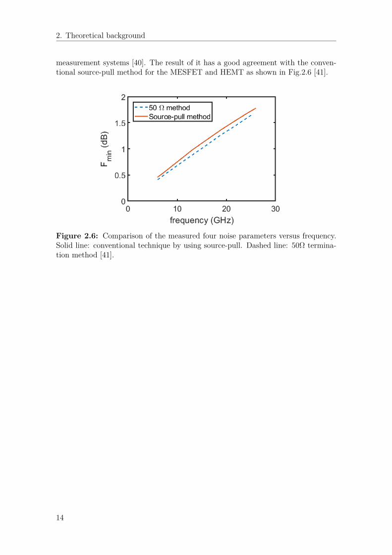
measurement systems [40]. The result of it has a good agreement with the conven-tional source-pull method for the MESFET and HEMT as shown in Fig.2.6 [41].
Figure 2.6: Comparison of the measured four noise parameters versus frequency.Solid line: conventional technique by using source-pull. Dashed line: 50Ω termina-tion method [41].
14
3Fabrication and characterisation of
GFETs
In this chapter, the experimental process and noise results of the GFETs are il-lustrated. Device fabrication, dc characterisation, S-parameters and noise figuremeasured at different ambient temperature and bias conditions are shown. Thenoise measurements are carried out in a noise parameter characterisation setup us-ing the cold-source method with 50 Ω termination. An empirical noise model forthe GFET on temperature and gate bias dependence is proposed at the end of thischapter which is necessary for the future design of graphene low-noise amplifiers.
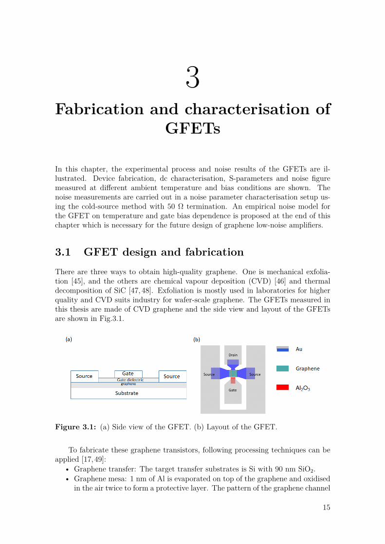
3.1 GFET design and fabricationThere are three ways to obtain high-quality graphene. One is mechanical exfolia-tion [45], and the others are chemical vapour deposition (CVD) [46] and thermaldecomposition of SiC [47, 48]. Exfoliation is mostly used in laboratories for higherquality and CVD suits industry for wafer-scale graphene. The GFETs measured inthis thesis are made of CVD graphene and the side view and layout of the GFETsare shown in Fig.3.1.
Figure 3.1: (a) Side view of the GFET. (b) Layout of the GFET.
To fabricate these graphene transistors, following processing techniques can beapplied [17,49]:
• Graphene transfer: The target transfer substrates is Si with 90 nm SiO2.• Graphene mesa: 1 nm of Al is evaporated on top of the graphene and oxidised
in the air twice to form a protective layer. The pattern of the graphene channel
15

3. Fabrication and characterisation of GFETs
is defined by e-beam lithography. Other parts of graphene are etched by oxygenplasma.
• Ohmic contact: The electrodes of source and drain are patterned by E-beamlithography and lift-off process.
• Gate dielectric: Al2O3 dielectric is formed by evaporation 1 nm Al and naturaloxidation in the air for six times.
• Gate contact: E-beam lithography is applied again to form the gate contactpattern and evaporate 10 nm Ti or 200 nm Au on the dielectric.
• Pad contacts: The contact pads are formed after a final e-beam lithographyand Ti or Au evaporation.
Fig.3.2 displays the SEM image of the GFET [50] that is fabricated from theabove process and measured in the following experiments. The GFET has a gate of0.75× 15 µm2.
Figure 3.2: SEM image of a two-finger GFET with gate length Lg = 0.75 µm andgate width Wg = 2× 15 µm. The inset shows a 70 tilted view of the gate area [49].
3.2 DC characteristics
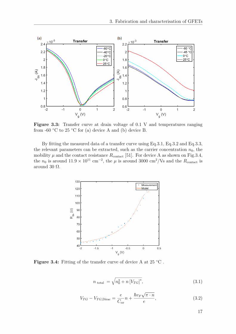
Fig.3.3a shows the drain current versus gate voltage at different temperatures fordevice A which has a 0.75 × 15 µm2 gate. The Dirac point of device A is around0.1 V. The transfer curve of device A does not change too much under differenttemperatures. The shift of the Dirac point is within 0.1 V. However, the Diracpoint of many other devices will shift a lot when temperature changes, like device B(with 0.75×15 µm2 gate) shown in Fig.3.3b. In order to simplify the characterisationand modelling, we will focus on device A first. In this case, the effect of the changeof the Dirac point won’t be considered in the later discussion.
16
3. Fabrication and characterisation of GFETs
Figure 3.3: Transfer curve at drain voltage of 0.1 V and temperatures rangingfrom -60 C to 25 C for (a) device A and (b) device B.
By fitting the measured data of a transfer curve using Eq.3.1, Eq.3.2 and Eq.3.3,the relevant parameters can be extracted, such as the carrier concentration n0, themobility µ and the contact resistance Rcontact [51]. For device A as shown on Fig.3.4,the n0 is around 11.9× 1011 cm−2, the µ is around 3000 cm2/Vs and the Rcontact isaround 30 Ω.
Figure 3.4: Fitting of the transfer curve of device A at 25 C .
n total =√n2
0 + n [VTG]∗, (3.1)
VTG − VTG,Dirac = e
Coxn+ ~vF
√π · ne
, (3.2)
17

3. Fabrication and characterisation of GFETs
Rtotal = Rcontact+Rchannel = Rcontact+Nsq
n total eµ= Rcontact+
Nsq√n2
0 + n [V ∗TG]2eµ
. (3.3)
For the output curve, we can see from Fig.3.5a that at -60 C it has a highercurrent than that of 25 C which is the same as expectation. This is mainly becauseof the decrease in the contact resistance at lower temperature. But if it is cooleddown to cryogenic temperature as shown in Fig.3.5b, the drain current at 4k is evenlower than that of 25 C. This phenomenon may come from the change of otherparameters at a very low temperature.
Figure 3.5: Output curve of device A at gate voltage from -1.2 V to 0.6 V in stepsof 0.2 V (a) at 213 K and 300 K, respectively, and (b) at 4 K and 300 K, respectively.
3.3 S-parameters
The S-parameters are important for the extraction of the Fmin according to theprevious chapter. Therefore it is necessary to check how the S-parameters changewith temperatures. Fig.3.6 shows the S11, S12, S21, and S22, of device A with drainvoltage of -1.2 V and gate voltage of -0.7 V at five different temperatures. It isobvious that S21, the complex linear gain, is affected most by the temperature.
The intrinsic parameters extracted from the S-parameters in the frequency rangeof 2 - 18 GHz at 298 k and 213 K are shown in Table.3.1 [43,44]. Fig.3.7 shows theintrinsic transconductance (gmi) at different ambient temperatures. Due to the shortgate length, gmi of the device is proportional to the number of carriers and theirsaturation velocity in the channel. Here it shows an approximately linear decreasewith temperature which means the velocity saturation and the carrier density alsohave some dependence on temperature.
18
3. Fabrication and characterisation of GFETs
Figure 3.6: S-parameters of device A at Vg = -0.7 V Vd = -1.2 V at -60, -40, -20,0 and 25 C respectively.
Figure 3.7: The intrinsic transconductance at Vg = -0.7 V, Vd = 1.2 V at differenttemperatures.
19
3. Fabrication and characterisation of GFETs
Table 3.1: De-embedded parameters for the GFET at Vgs = -0.7 V, Vds = -1.2 Vand ambient temperature of 213 K and 298 K.
T Cgs Cgd Cds gds gmi τ Ri
(K) (fF) (fF) (fF) (mS) (mS) (ps) (Ω)298 27 26 20 7.7 4.1 0.10 3.4213 25 25 17 6.8 5.1 0.13 4.8
3.4 Noise characterisation
3.4.1 Measurement setups
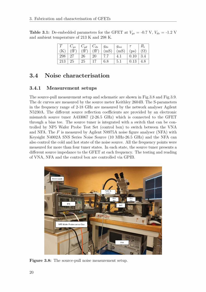
The source-pull measurement setup and schematic are shown in Fig.3.8 and Fig.3.9.The dc curves are measured by the source meter Keithley 2604B. The S-parametersin the frequency range of 2-18 GHz are measured by the network analyser AgilentN5230A. The different source reflection coefficients are provided by an electronicmismatch source tuner A433067 (2-26.5 GHz) which is connected to the GFETthrough a bias tee. The source tuner is integrated with a switch that can be con-trolled by NP5 Wafer Probe Test Set (control box) to switch between the VNAand NFA. The F is measured by Agilent N8975A noise figure analyser (NFA) withKeysight N4002A SNS Series Noise Source (10 MHz-26.5 GHz) and the NFA canalso control the cold and hot state of the noise source. All the frequency points weremeasured for more than four tuner states. In each state, the source tuner presents adifferent source impedance to the GFET at each frequency. The testing and readingof VNA, NFA and the control box are controlled via GPIB.
Figure 3.8: The source-pull noise measurement setup.
20

3. Fabrication and characterisation of GFETs
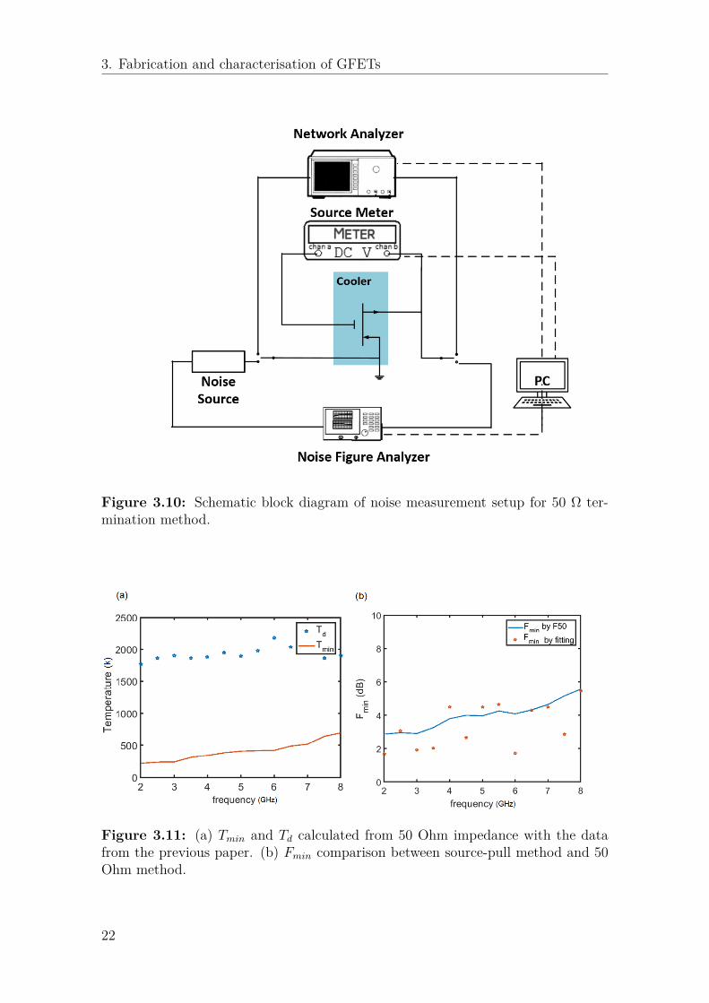
The 50 Ω termination method doesn’t need the tuner and the setup schematicis shown in Fig.3.10. The dc curves are also measured by the source meter Keith-ley 2604B. The S-parameters in the frequency range of 2-18 GHz are measured bythe network analyser (VNA) Agilent E8361A. And the F50 of the GFET was mea-sured by Keysight N4002ASNS Series Noise Source and Agilent N8975A noise figureanalyser (NFA) connected through a bias tee. The measurements are controlledvia GPIB. The results between these two methods are compared in Fig.3.11 whichshows that they are quite comparable. Since this method is easier and time-saving,the temperature changing experiments will use this 50 Ω method. The GFET andcalibration kits are put in the thermal truck in advance. The chamber temperatureis cooled down to -60 C firstly and increased step by step up to -25 C.
The Fmin of GFETs in the previous paper are all measured by the source-pullmethod [17,18]. The 50 Ω method has never been used for GFETs. We take the sameF50 and S-parameters from the previous paper [17] and calculate the Fmin and Tminusing 50 Ω method and compare it with the result in the paper which are measuredby source-pull method. Fig.3.11a shows that the Tmin extracted from the F50 is inthe range of 200 K to 600 K at the frequency of 2-8 GHz which is approximatelythe same as that shown in the paper [17]. Fig.3.11b shows the comparison of Fminbetween that calculated by F50 and that converted from the Tmin in paper [17].Theyare quite consistent with each other which means the F50 noise measurement methodworks as well as the source-pull method for GFET.
Figure 3.9: Schematic of source-pull noise measurement setup.
21
3. Fabrication and characterisation of GFETs
Figure 3.10: Schematic block diagram of noise measurement setup for 50 Ω ter-mination method.
Figure 3.11: (a) Tmin and Td calculated from 50 Ohm impedance with the datafrom the previous paper. (b) Fmin comparison between source-pull method and 50Ohm method.
22

3. Fabrication and characterisation of GFETs
3.4.2 Fmin at different temperatures and bias voltagesThe noise parameters are measured versus bias and frequency at different temper-atures. For device A which has no Dirac point shift, the Fmin versus frequency of2-18 GHz is shown in Fig.3.12a. It was operated at five different temperatures withthe same gate and drain bias. The Fmin at room temperature is higher than -60C as expected, which is partly due to the temperature dependence of the accessresistance RS and RD. And Fig.3.12b shows that the Fmin increases approximatelylinear with the frequency which is consistent with the other FETs.
Figure 3.12: (a) Fmin versus frequency of device A at different temperatures (-60C, -40 C, -20 C, 0 C and 25 C) with gate voltage of -0.1 V and drain voltageof -1.4 V. (b) Fmin versus temperature of device A for different frequencies (12, 14,16, and 18 GHz) at gate voltage of -0.1 V and drain voltage of -1.4V.
As we know, the slop of the drain current at very low voltage is an importantindicator of the noise performance of a device. From Fig.3.12b we know that thenoise is lower at -60 C compared with room temperature and that is what we can seefrom the output curves in Fig.3.5a. But it is opposite at cryogenic temperature asshown in Fig.3.5b, which indicates that the noise of graphene transistor at cryogenictemperature is even higher.
the Fmin increases linearly with frequency, this noise characterisation of GFETis carried out at 6.5 GHz by random and the ambient temperatures range is 237-297K. The contours of the Fmin are plotted. The x-axis is the temperature from -60C to 25 C and the Y-axis is the gate voltage. The number on the contour line isthe Fmin in decibel. And these four plots are measured at the drain voltage of -0.8V, -1 V, -1.2 V and -1.4 V, respectively. With these contour plots, we can see howthe noise figure changes with temperature and gate voltage at the same time. Andcontours of the Fmin with both drain and gate bias are displayed on Fig.3.14. Itshows that Fmin is relatively stable with drain bias. These plots show that the noiseperformance of the GFET is insensitive to changes in Vds but very sensitive to Vgsand temperature. It is because Vgs changes the carrier density while increasing Vdsleads to saturation of velocity.
23

3. Fabrication and characterisation of GFETs
Figure 3.13: Fmin in decibel of device A versus temperature at 6.5 GHz and drainbias of -0.8, -1, -1.2, -1.4 V respectively
Figure 3.14: Fmin in decibel of device A versus drain bias at 6.5 GHz and -60, -20,0, and 25 C respectively
24
3. Fabrication and characterisation of GFETs
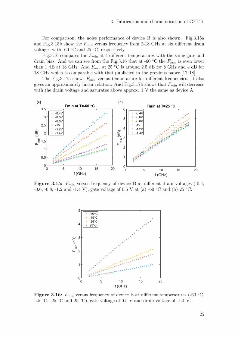
For comparison, the noise performance of device B is also shown. Fig.3.15aand Fig.3.15b show the Fmin versus frequency from 2-18 GHz at six different drainvoltages with -60 C and 25 C, respectively.
Fig.3.16 compares the Fmin at 4 different temperatures with the same gate anddrain bias. And we can see from the Fig.3.16 that at -60 C the Fmin is even lowerthan 1 dB at 18 GHz. And Fmin at 25 C is around 2.5 dB for 8 GHz and 4 dB for18 GHz which is comparable with that published in the previous paper [17,18].
The Fig.3.17a shows Fmin versus temperature for different frequencies. It alsogives an approximately linear relation. And Fig.3.17b shows that Fmin will decreasewith the drain voltage and saturates above approx. 1 V the same as device A.
Figure 3.15: Fmin versus frequency of device B at different drain voltages (-0.4,-0.6, -0.8, -1.2 and -1.4 V), gate voltage of 0.5 V at (a) -60 C and (b) 25 C.
Figure 3.16: Fmin versus frequency of device B at different temperatures (-60 C,-45 C, -25 C and 25 C), gate voltage of 0.5 V and drain voltage of -1.4 V.
25
3. Fabrication and characterisation of GFETs
Figure 3.17: (a) Fmin versus temperature of device B at drain voltage of -1.4Vand (b) Fmin versus drain voltage of device B at ambient temperature of -60 C, fordifferent frequencies (2, 6, 10, 14 and 18 GHz) at gate voltage of 0.5 V.
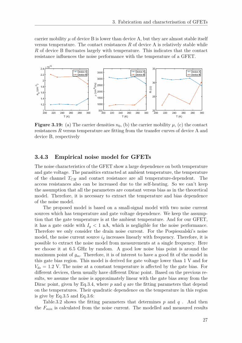
Device B has a higher maximum frequency of oscillation (fmax) of 18 GHz and21 GHz at 25 C and -60 C respectively. While for device A, the fmax is only 14GHz and 16 GHz for 25 C and -60 C respectively. The noise of device B at -60 Cis much lower than device A as shown in Fig.3.18. And the slope of the line whichshows the Fmin versus temperature, device B is larger than device A which meansdevice B is more sensitive to temperature.
Figure 3.18: Fmin versus temperature for device A and B at 12 GHz and drainvoltage of -1.4 V.
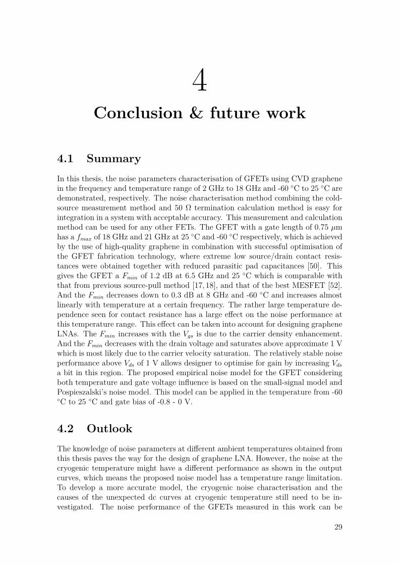
In order to find out which is the key factor of the temperature dependence, theextract parameters fitting from the transfer curves of these two devices are comparedin Fig.3.19. The carrier densities n0 of device B is higher than device A and the
26
3. Fabrication and characterisation of GFETs
carrier mobility µ of device B is lower than device A, but they are almost stable itselfversus temperature. The contact resistances R of device A is relatively stable whileR of device B fluctuates largely with temperature. This indicates that the contactresistance influences the noise performance with the temperature of a GFET.
Figure 3.19: (a) The carrier densities n0, (b) the carrier mobility µ, (c) the contactresistances R versus temperature are fitting from the transfer curves of device A anddevice B, respectively
3.4.3 Empirical noise model for GFETsThe noise characteristics of the GFET show a large dependence on both temperatureand gate voltage. The parasitics extracted at ambient temperature, the temperatureof the channel TCH and contact resistance are all temperature-dependent. Theaccess resistances also can be increased due to the self-heating. So we can’t keepthe assumption that all the parameters are constant versus bias as in the theoreticalmodel. Therefore, it is necessary to extract the temperature and bias dependenceof the noise model.
The proposed model is based on a small-signal model with two noise currentsources which has temperature and gate voltage dependence. We keep the assump-tion that the gate temperature is at the ambient temperature. And for our GFET,it has a gate oxide with Ig < 1 nA, which is negligible for the noise performance.Therefore we only consider the drain noise current. For the Pospieszalski’s noisemodel, the noise current source id increases linearly with frequency. Therefore, it ispossible to extract the noise model from measurements at a single frequency. Herewe choose it at 6.5 GHz by random. A good low noise bias point is around themaximum point of gm. Therefore, it is of interest to have a good fit of the model inthis gate bias region. This model is derived for gate voltage lower than 1 V and forVds = 1.2 V. The noise at a constant temperature is affected by the gate bias. Fordifferent devices, them usually have different Dirac point. Based on the previous re-sults, we assume the noise is approximately linear with the gate bias away from theDirac point, given by Eq.3.4, where p and q are the fitting parameters that dependon the temperatures. Their quadratic dependence on the temperature in this regionis give by Eq.3.5 and Eq.3.6:
Table.3.2 shows the fitting parameters that determines p and q . And thenthe Fmin is calculated from the noise current. The modelled and measured results
27

3. Fabrication and characterisation of GFETs
are both shown on the Fig.3.20. The Fmin decreases with Vgs and increases withfrequency. This model works very well at the temperature range from -60 C to25 C and gate bias from 0 to -0.8V. This more accurate model can be used ina computer-aided design (CAD) software package and makes it possible to obtainoptimum low noise performance at an arbitrary temperature.
idf
= p |Vgs − Vdirac|+ q, (3.4)
p = a1T2 + a2T + a3, (3.5)
q = b1T2 + b2T + b3, (3.6)
Table 3.2: Fitting parameters of the GFET noise model.
x 1 2 3ax -1.5E-10 4.9E-08 -8.1E-06bx -1.4E-10 9.3E-08 -6.8E-06
Figure 3.20: Modelled (line) and measured (circle) noise parameters for GFETwith Vds = 1.2 V (a) at frequency of 6.5 GHz and (b) Vgs at -0.1 V with temperatureof -60 C (blue), -20 C (black) and 25 C (red), respectively.
28
4Conclusion & future work
4.1 SummaryIn this thesis, the noise parameters characterisation of GFETs using CVD graphenein the frequency and temperature range of 2 GHz to 18 GHz and -60 C to 25 C aredemonstrated, respectively. The noise characterisation method combining the cold-source measurement method and 50 Ω termination calculation method is easy forintegration in a system with acceptable accuracy. This measurement and calculationmethod can be used for any other FETs. The GFET with a gate length of 0.75 µmhas a fmax of 18 GHz and 21 GHz at 25 C and -60 C respectively, which is achievedby the use of high-quality graphene in combination with successful optimisation ofthe GFET fabrication technology, where extreme low source/drain contact resis-tances were obtained together with reduced parasitic pad capacitances [50]. Thisgives the GFET a Fmin of 1.2 dB at 6.5 GHz and 25 C which is comparable withthat from previous source-pull method [17, 18], and that of the best MESFET [52].And the Fmin decreases down to 0.3 dB at 8 GHz and -60 C and increases almostlinearly with temperature at a certain frequency. The rather large temperature de-pendence seen for contact resistance has a large effect on the noise performance atthis temperature range. This effect can be taken into account for designing grapheneLNAs. The Fmin increases with the Vgs is due to the carrier density enhancement.And the Fmin decreases with the drain voltage and saturates above approximate 1 Vwhich is most likely due to the carrier velocity saturation. The relatively stable noiseperformance above Vds of 1 V allows designer to optimise for gain by increasing Vdsa bit in this region. The proposed empirical noise model for the GFET consideringboth temperature and gate voltage influence is based on the small-signal model andPospieszalski’s noise model. This model can be applied in the temperature from -60C to 25 C and gate bias of -0.8 - 0 V.
4.2 OutlookThe knowledge of noise parameters at different ambient temperatures obtained fromthis thesis paves the way for the design of graphene LNA. However, the noise at thecryogenic temperature might have a different performance as shown in the outputcurves, which means the proposed noise model has a temperature range limitation.To develop a more accurate model, the cryogenic noise characterisation and thecauses of the unexpected dc curves at cryogenic temperature still need to be in-vestigated. The noise performance of the GFETs measured in this work can be
29

4. Conclusion & future work
comparable with Si CMOS and MESFET, but it still needs to be improved to becomparable with GaAs or InP HEMTs [53, 54]. The fT and fmax also need to beincreased in order to extend to higher frequencies. The fT and fmax are not as highas the expectation which is because the carrier mobility in graphene doesn’t reachthe expectation in the theory. This is due to the impurity introduced during fabrica-tion. Some methods have been proposed to solve it, such as using hexagonal boronnitride (hBN) capsulation by an advanced dry van-der Waals transfer method [55].For the structure, the gate width can be lager to increase the capacitance and thegate length can be shorter by using T-shape to decrease the contact resistance [56].Consequently, it will provide GFETs with a better noise performance.
30

Bibliography
[1] P. H. Siegel, “Terahertz technology in biology and medicine,” IEEE Transac-tions on Microwave Theory and Techniques, vol. 52, no. 10, pp. 2438–2447, Oct2004. doi: 10.1109/TMTT.2004.835916
[2] R. Appleby and R. N. Anderton, “Millimeter-wave and submillimeter-waveimaging for security and surveillance,” Proceedings of the IEEE, vol. 95, no. 8,pp. 1683–1690, Aug 2007. doi: 10.1109/JPROC.2007.898832
[3] S. Rangan, T. S. Rappaport, and E. Erkip, “Millimeter-wave cellular wirelessnetworks: Potentials and challenges,” Proceedings of the IEEE, vol. 102, no. 3,pp. 366–385, March 2014. doi: 10.1109/JPROC.2014.2299397
[4] W. Shockley, “A unipolar "field-effect" transistor,” Proceedings of the IRE,vol. 40, no. 11, pp. 1365–1376, Nov 1952. doi: 10.1109/JRPROC.1952.273964
[5] T. Mimura, “The early history of the high electron mobility transistor(HEMT),” Microwave Theory and Techniques, IEEE Transactions on, vol. 50,pp. 780 – 782, 04 2002. doi: 10.1109/22.989961
[6] L. A. Samoska, “An overview of solid-state integrated circuit amplifiers inthe submillimeter-wave and THz regime,” IEEE Transactions on TerahertzScience and Technology, vol. 1, no. 1, pp. 9–24, Sep. 2011. doi: 10.1109/T-THZ.2011.2159558
[7] K. S. Novoselov, A. K. Geim, S. V. Morozov, D. Jiang, Y. Zhang, S. V.Dubonos, I. V. Grigorieva, and A. A. Firsov, “Electric field effect in atomi-cally thin carbon films,” Science, vol. 306, no. 5696, pp. 666–669, 2004. doi:10.1126/science.1102896
[8] K. Bolotin, K. Sikes, Z. Jiang, M. Klima, G. Fudenberg, J. Hone, P. Kim,and H. Stormer, “Ultrahigh electron mobility in suspended graphene,”Solid State Communications, vol. 146, no. 9, pp. 351 – 355, 2008. doi:10.1016/j.ssc.2008.02.024
[9] M. C. Lemme, T. J. Echtermeyer, M. Baus, and H. Kurz, “A graphene field-effect device,” IEEE Electron Device Letters, vol. 28, no. 4, pp. 282–284, April2007. doi: 10.1109/LED.2007.891668
[10] F. Schwierz, “Graphene transistors,” Nature Nanotechnology, vol. 5, p. 487,2010. doi: 10.1038/nnano.2010.89
[11] X. Yang, A. Vorobiev, A. Generalov, M. A. Andersson, and J. Stake, “A flexiblegraphene terahertz detector,” Applied Physics Letters, vol. 111, no. 2, p. 021102,2017. doi: 10.1063/1.4993434
[12] M. S. Gupta, “Power gain in feedback amplifiers, a classic revisited,” IEEETransactions on Microwave Theory and Techniques, vol. 40, no. 5, pp. 864–879, May 1992. doi: 10.1109/22.137392
31
Bibliography
[13] S. J. Mason, “Feedback theory-some properties of signal flow graphs,” Proceed-ings of the IRE, vol. 41, no. 9, pp. 1144–1156, Sep. 1953. doi: 10.1109/JR-PROC.1953.274449
[14] F. Schwierz, “Graphene transistors: Status, prospects, and problems,” Pro-ceedings of the IEEE, vol. 101, no. 7, pp. 1567–1584, July 2013. doi:10.1109/JPROC.2013.2257633
[15] M.Andersson., “Characterisation and modelling of graphene FETs for terahertzmixers and detectors.” Chalmers Doctor thesis, 2016.
[16] M. A. Andersson, O. Habibpour, J. Vukusic, and J. Stake, “10 dB small-signalgraphene FET amplifier,” Electronics Letters, vol. 48, no. 14, pp. 861–863, July2012. doi: 10.1049/el.2012.1347
[17] M. Tanzid, M. A. Andersson, J. Sun, and J. Stake, “Microwave noise charac-terization of graphene field effect transistors,” Applied Physics Letters, vol. 104,no. 1, p. 013502, 2014. doi: 10.1063/1.4861115
[18] C. Yu, Z. Z. He, X. B. Song, Q. B. Liu, S. B. Dun, T. T. Han, J. J. Wang, C. J.Zhou, J. C. Guo, Y. J. Lv, S. J. Cai, and Z. H. Feng, “High-frequency noisecharacterization of graphene field effect transistors on SiC substrates,” AppliedPhysics Letters, vol. 111, no. 3, p. 033502, 2017. doi: 10.1063/1.4994324
[19] C.-H. Yeh, Y.-W. Lain, Y.-C. Chiu, C.-H. Liao, D. Ricardo Moyano, S. S H Hsu,and P.-W. Chiu, “GHz flexible graphene transistors for microwave integratedcircuits.” ACS nano, vol. 8, 07 2014. doi: 10.1021/nn5036087
[20] A. J. Scholten, L. F. Tiemeijer, R. van Langevelde, R. J. Havens, A. T. A.Zegers-van Duijnhoven, and V. C. Venezia, “Noise modeling for RF CMOScircuit simulation,” IEEE Transactions on Electron Devices, vol. 50, no. 3, pp.618–632, March 2003. doi: 10.1109/TED.2003.810480
[21] Jung-Suk Goo, Chang-Hoon Choi, E. Morifuji, H. S. Momose, Zhiping Yu,H. Iwai, T. H. Lee, and R. W. Dutton, “RF noise simulation for submicronMOSFET’s based on hydrodynamic model,” in 1999 Symposium on VLSI Tech-nology. Digest of Technical Papers (IEEE Cat. No.99CH36325), June 1999. doi:10.1109/VLSIT.1999.799389 pp. 153–154.
[22] J. Wenger, “Quarter-micrometer low-noise pseudomorphic GaAs HEMTs withextremely low dependence of the noise figure on drain-source current,”IEEE Electron Device Letters, vol. 14, no. 1, pp. 16–18, Jan 1993. doi:10.1109/55.215086
[23] P. Ho, P. C. Chao, K. H. G. Duh, A. A. Jabra, J. M. Ballingall, and P. M. Smith,“Extremely high gain, low noise InAlAs/InGaAs HEMTs grown by molecularbeam epitaxy,” pp. 184–186, Dec 1988. doi: 10.1109/IEDM.1988.32785
[24] G. Gonzalez, Microwave Transistor Amplifiers: Analysis and Design.Prentice Hall, 1997. ISBN 9780132543354. [Online]. Available: https://books.google.se/books?id=-AVTAAAAMAAJ
[25] J. B. Johnson, “Thermal agitation of electricity in conductors,” Phys. Rev.,vol. 32, pp. 97–109, Jul 1928. doi: 10.1103/PhysRev.32.97
[26] H. Nyquist, “Thermal agitation of electric charge in conductors,” Phys. Rev.,vol. 32, pp. 110–113, Jul 1928. doi: 10.1103/PhysRev.32.110
32
Bibliography
[27] G. H. Hanson and A. V. Der Ziel, “Shot noise in transistors,” Proceedingsof the IRE, vol. 45, no. 11, pp. 1538–1542, Nov 1957. doi: 10.1109/JR-PROC.1957.278349
[28] V. Mitin, L. Reggiani, and L. Varani., “Noise and fluctuations control in elec-tronic devices.” American Scientific Publishers, 2002.
[29] S. Maas., “Noise in linear and nonlinear circuits.” Artech House, 2005.[30] H. T. Friis, “Noise figures of radio receivers,” Proceedings of the IRE, vol. 32,
no. 7, pp. 419–422, July 1944. doi: 10.1109/JRPROC.1944.232049[31] H. Fukui, “Available power gain, noise figure, and noise measure of two-ports
and their graphical representations,” IEEE Transactions on Circuit Theory,vol. 13, no. 2, pp. 137–142, June 1966. doi: 10.1109/TCT.1966.1082556
[32] F. Schwierz and J. Liou., “Modern microwave transistors: Theory, design andperformance.” Hoboken, New Jersey: John Wiley and Sons, 2003.
[33] M. Pospieszalski, “Modeling of noise parameters of MESFETs and MOD-FETs and their frequency and temperature dependence,” Microwave Theoryand Techniques, IEEE Transactions on, vol. 37, pp. 1340–1350, 09 1989. doi:10.1109/22.32217
[34] H. Rothe and W. Dahlke, “Theory of noisy fourpoles,” Proceedings of the IRE,vol. 44, no. 6, pp. 811–818, June 1956. doi: 10.1109/JRPROC.1956.274998
[35] M. Pospieszalski, “Interpreting transistor noise.” Microwave Magazine, IEEE,vol. 11, pp. 61 – 69, 2010.
[36] M. A. Andersson and J. Stake, “An accurate empirical model based onvolterra series for FET power detectors,” IEEE Transactions on MicrowaveTheory and Techniques, vol. 64, no. 5, pp. 1431–1441, May 2016. doi:10.1109/TMTT.2016.2532326
[37] K. Technologies, “Fundamentals of rf and microwave noise figure measure-ments.” Keysight Technologies Application note.
[38] N. Otegi, J. M. Collantes, and M. Sayed, “Cold-source measurements for noisefigure calculation in spectrum analyzers,” in 2006 67th ARFTG Conference,June 2006. doi: 10.1109/ARFTG.2006.4734387 pp. 223–228.
[39] D. M. Pozar., “Microwave engineering, 4th edition.” Wiley Global EducationUS, vol. 11, 2011.
[40] P. J. Tasker, W. Reinert, J. Braunstein, and M. Schlechtweg, “Direct extrac-tion of all four transistor noise parameters from a single noise figure measure-ment,” in 1992 22nd European Microwave Conference, vol. 1, 09 1992. doi:10.1109/EUMA.1992.335733 pp. 157–162.
[41] G. Dambrine, H. Happy, F. Danneville, and A. Cappy, “A new method foron wafer noise measurement,” IEEE Transactions on Microwave Theory andTechniques, vol. 41, no. 3, pp. 375–381, March 1993. doi: 10.1109/22.223734
[42] B. Hughes, “A temperature noise model for extrinsic FETs,” IEEE Transactionson Microwave Theory and Techniques, vol. 40, no. 9, pp. 1821–1832, Sep. 1992.doi: 10.1109/22.156610
[43] M. Berroth and R. Bosch, “Broad-band determination of the FET small-signalequivalent circuit,” IEEE Transactions on Microwave Theory and Techniques,vol. 38, no. 7, pp. 891–895, 07 1990. doi: 10.1109/22.55781
33
Bibliography
[44] G. Dambrine, A. Cappy, F. Heliodore, and E. Playez, “A new method fordetermining the FET small-signal equivalent circuit,” IEEE Transactions onMicrowave Theory and Techniques, vol. 36, no. 7, pp. 1151–1159, July 1988.doi: 10.1109/22.3650
[45] M. Yi and Z. Shen, “A review on mechanical exfoliation for the scalable pro-duction of graphene,” J. Mater. Chem. A, vol. 3, pp. 11 700–11 715, 2015. doi:10.1039/C5TA00252D
[46] G. Deokar, J. Avila, I. Razado-Colambo, J.-L. Codron, C. Boyaval,E. Galopin, M.-C. Asensio, and D. Vignaud, “Towards high quality CVDgraphene growth and transfer,” Carbon, vol. 89, pp. 82 – 92, 2015. doi:10.1016/j.carbon.2015.03.017
[47] C. Berger, Z. Song, X. Li, X. Wu, N. Brown, C. Naud, D. Mayou, T. Li, J. Hass,A. N. Marchenkov, E. H. Conrad, P. N. First, and W. A. de Heer, “Electronicconfinement and coherence in patterned epitaxial graphene,” Science, vol. 312,no. 5777, pp. 1191–1196, 2006. doi: 10.1126/science.1125925
[48] J. Kedzierski, P. Hsu, P. Healey, P. Wyatt, and C. Keast, “Epitaxial graphenetransistors on SiC substrates,” in 2008 Device Research Conference, June 2008.doi: 10.1109/DRC.2008.4800720. ISSN 1548-3770 pp. 25–26.
[49] S. Bidmeshkipour, A. Vorobiev, M. A. Andersson, A. Kompany, and J. Stake,“Effect of ferroelectric substrate on carrier mobility in graphene field-effecttransistors,” Applied Physics Letters, vol. 107, no. 17, p. 173106, 2015. doi:10.1063/1.4934696
[50] M. Bonmann, M. Asad, X. Yang, A. Generalov, A. Vorobiev, L. Banszerus,C. Stampfer, M. Otto, D. Neumaier, and J. Stake, “Graphene field-effect tran-sistors with high extrinsic fT and fmax,” IEEE Electron Device Letters, vol. 40,no. 1, pp. 131–134, Jan 2019. doi: 10.1109/LED.2018.2884054
[51] S. Kim, J. Nah, I. Jo, D. Shahrjerdi, L. Colombo, Z. Yao, E. Tutuc, andS. K. Banerjee, “Realization of a high mobility dual-gated graphene field-effecttransistor with Al2O3 dielectric,” Applied Physics Letters, vol. 94, no. 6, p.062107, 2009. doi: 10.1063/1.3077021
[52] Z. Ramezani, A. A. Orouji, and M. Rahimian, “High-performance SOI MES-FET with modified depletion region using a triple recessed gate for RF appli-cations,” Materials Science in Semiconductor Processing, vol. 30, pp. 75 – 84,2015. doi: 10.1016/j.mssp.2014.09.023
[53] J. Wenger, “Quarter-micrometer low-noise pseudomorphic GaAs HEMTs withextremely low dependence of the noise figure on drain-source current,”IEEE Electron Device Letters, vol. 14, no. 1, pp. 16–18, Jan 1993. doi:10.1109/55.215086
[54] J. Schleeh, G. Alestig, J. Halonen, A. Malmros, B. Nilsson, P. A. Nils-son, J. P. Starski, N. Wadefalk, H. Zirath, and J. Grahn, “Ultralow-powercryogenic InP HEMT with minimum noise temperature of 1 K at 6 GHz,”IEEE Electron Device Letters, vol. 33, no. 5, pp. 664–666, May 2012. doi:10.1109/LED.2012.2187422
[55] L. Banszerus, M. Schmitz, S. Engels, M. Goldsche, K. Watanabe, T. Taniguchi,B. Beschoten, and C. Stampfer, “Ballistic transport exceeding 28 µ m
34

Bibliography
in CVD grown graphene,” Nano letters, vol. 16, p. 1387, 01 2016. doi:10.1021/acs.nanolett.5b04840
[56] E. Cha, G. Moschetti, N. Wadefalk, P. Nilsson, S. Bevilacqua, A. Pourkabirian,P. Starski, and J. Grahn, “Two-finger InP HEMT design for stable cryogenicoperation of ultra-low-noise Ka- and Q-band LNAs,” IEEE Transactions onMicrowave Theory and Techniques, vol. 65, no. 12, pp. 5171–5180, Dec 2017.doi: 10.1109/TMTT.2017.2765318
35
Bibliography
36

AMatlab code
The Matlab files for analysis of Fmin are encoded.
A.1 Main file
1
2 %% Noise parameter characterization3 instrreset ;4 clear all ;5 close all ;6 clc ;7 path(path,’code’) ;8
9 %% Setup10
11 % measurement frequency12
13 setup. fstart = 2; % start frequency in GHz14 setup.fstop = 18; % stop frequency in GHz15 setup. fstep = .5; % step frequency in GHz16
17 % delay in through standard18
19 setup.delay=0;20 data.freq = 2:.5:18;21 freq = 2:.5:18;22
23 % ENR of the reference noise source24
25 NoiseSourceFile = ’enr’ ;26
27 setup.averaging = 8; % number of averages done, 1 − 51228 setup.rf_atten = 30; % rf attenuation setting (1 − 6), 0 = auto29 setup.if_atten = 0;30
31 % vna settings Anritsu32 setup.vna_start = setup.fstart.∗1e3;33 setup.vna_step = setup.fstep.∗1e3;34 setup.vna_points = length(data.freq);35 setup.vna_pwr = −10;36 setup.vna_att1 = 20;37 setup.vna_att2 = 20;38 setup.vna_IFBW = ’IF1’;% ’IF1’=10 Hz,’IF2’=100 Hz ’IF3’=1000 Hz ’IF4’=10000 Hz
I

A. Matlab code
39 setup.DutCalset = 2;40 setup.GsCalset = 3;41 setup.GlCalset = 4;42
43 %% Initilize measurement system44 instr = init_atn_nfa(setup);45
46
47 %% perform noise port calibration48 input(’Connect through at DUT plane’);49 Calibration = NoisePortCal_onwafer(instr);50
51 %% Read 50 ohm hot cold noise52 input(’Connect noise source for 50ohm reference measurement and press ENTER’);53 [Calibration.G0kdf setup] = NoiseRef_nfa_sweep(instr, setup);54 save( ’data/calibration_cal’ , ’Calibration’ ) ;55
56 %% Connect the DUT to the VNA57 % turn on vna58 vna = get(instr.vna, ’ Interface ’ ) ;59 fprintf (vna, ’SINC;S22;DRIVPORT2’);60 fprintf (get( instr .vna,’ interface ’ ) , ’AVG 512’);61 fprintf (get( instr .vna,’ interface ’ ) , ’AVG 32’);62
63 % turn off vna64 fprintf (vna, ’S22;DRIVNONE’);65
66 %% Fix WinCal67 WinCalFix(instr.vna, setup);68
69 %% Correct noise port calibration70 [ns_gamma inputS] = NoisePortCorrection_onwafer(instr, Calibration, setup);71 Calibration.ns_gamma = ns_gamma;72 Calibration.inputS = inputS;73 save( ’data/calibration ’ , ’Calibration’ ) ;74
75 %% perform nfm gamma calibration76 % input(’Connect thru at DUT plane’);77 disp( ’Measures the gamma of receiver presented to dut’);78 Calibration.nfm_gamma = NFM_Gamma_onwafer(instr, setup);79 save( ’data/calibration ’ , ’Calibration’ ) ;80
81 %%82 % measure gammas presented to the DUT83 Calibration.GammaS = GammaSCal_onwafer(probe, carridge, instr, setup);84 save( ’data/calibration ’ , ’Calibration’ ) ;85
86 % perform recevier nosie parameter calibration87 % input(’Connect noise source and press ENTER’);88 [Calibration.RecNoise setup] = NoiseCal_nfa(Calibration, instr, setup);89 save( ’data/calibration ’ , ’Calibration’ ) ;90 % tmp = CorrectNoiseMeasure(RecNoise, G0kdf, ns_gamma, freq);91
92 % calculate noise parameters of receiver93 load(NoiseSourceFile);94 Calibration.Ta = 25; Calibration.Z0 = 50;
II
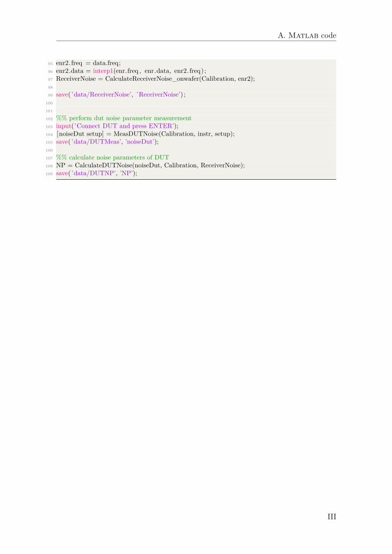
A. Matlab code
95 enr2. freq = data.freq;96 enr2.data = interp1(enr.freq , enr.data, enr2. freq) ;97 ReceiverNoise = CalculateReceiverNoise_onwafer(Calibration, enr2);98
99 save( ’data/ReceiverNoise’, ’ReceiverNoise’) ;100
101
102 %% perform dut noise parameter measurement103 input(’Connect DUT and press ENTER’);104 [noiseDut setup] = MeasDUTNoise(Calibration, instr, setup);105 save( ’data/DUTMeas’, ’noiseDut’);106
107 %% calculate noise parameters of DUT108 NP = CalculateDUTNoise(noiseDut, Calibration, ReceiverNoise);109 save( ’data/DUTNP’, ’NP’);
III

A. Matlab code
IV

BConference paper
High frequency noise characterisation of graphene field-effect transistorsat different temperatures
Junjie Li, Xinxin Yang, Marlene Bonmann, Muhammad Asad, Andrei Vorobiev,Jan Stake, Luca Banszerus, Christoph Stampfer, Martin Otto, Daniel Neumaier
In Graphene Week Conference, Helsinki, Finland, 2019.
V
www.graphene-flagship.eu
High frequency noise characterisation of graphene field-effect transistors at different temperatures
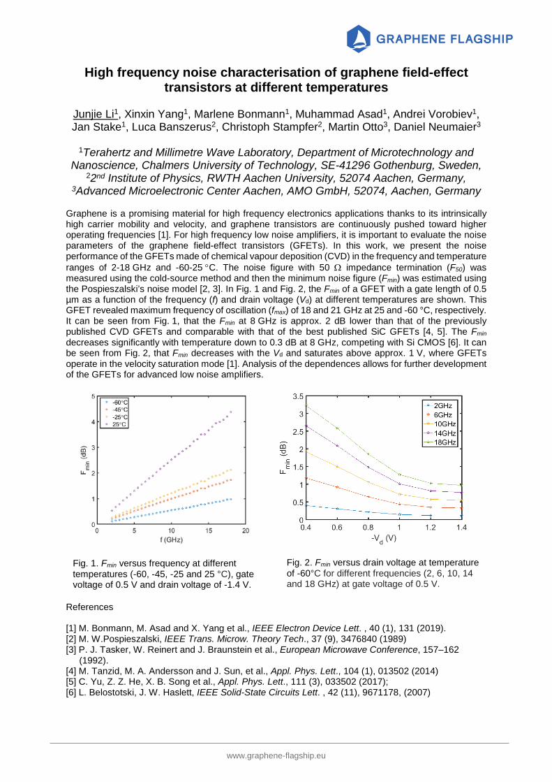
Junjie Li1, Xinxin Yang1, Marlene Bonmann1, Muhammad Asad1, Andrei Vorobiev1, Jan Stake1, Luca Banszerus2, Christoph Stampfer2, Martin Otto3, Daniel Neumaier3
1Terahertz and Millimetre Wave Laboratory, Department of Microtechnology and
Nanoscience, Chalmers University of Technology, SE-41296 Gothenburg, Sweden, 22nd Institute of Physics, RWTH Aachen University, 52074 Aachen, Germany,
3Advanced Microelectronic Center Aachen, AMO GmbH, 52074, Aachen, Germany Graphene is a promising material for high frequency electronics applications thanks to its intrinsically high carrier mobility and velocity, and graphene transistors are continuously pushed toward higher operating frequencies [1]. For high frequency low noise amplifiers, it is important to evaluate the noise parameters of the graphene field-effect transistors (GFETs). In this work, we present the noise performance of the GFETs made of chemical vapour deposition (CVD) in the frequency and temperature ranges of 2-18 GHz and -60-25 °C. The noise figure with 50 Ω impedance termination (F50) was measured using the cold-source method and then the minimum noise figure (Fmin) was estimated using the Pospieszalski’s noise model [2, 3]. In Fig. 1 and Fig. 2, the Fmin of a GFET with a gate length of 0.5 µm as a function of the frequency (f) and drain voltage (Vd) at different temperatures are shown. This GFET revealed maximum frequency of oscillation (fmax) of 18 and 21 GHz at 25 and -60 °C, respectively. It can be seen from Fig. 1, that the Fmin at 8 GHz is approx. 2 dB lower than that of the previously published CVD GFETs and comparable with that of the best published SiC GFETs [4, 5]. The Fmin decreases significantly with temperature down to 0.3 dB at 8 GHz, competing with Si CMOS [6]. It can be seen from Fig. 2, that Fmin decreases with the Vd and saturates above approx. 1 V, where GFETs operate in the velocity saturation mode [1]. Analysis of the dependences allows for further development of the GFETs for advanced low noise amplifiers.
References [1] M. Bonmann, M. Asad and X. Yang et al., IEEE Electron Device Lett. , 40 (1), 131 (2019). [2] M. W.Pospieszalski, IEEE Trans. Microw. Theory Tech., 37 (9), 3476840 (1989) [3] P. J. Tasker, W. Reinert and J. Braunstein et al., European Microwave Conference, 157–162
(1992). [4] M. Tanzid, M. A. Andersson and J. Sun, et al., Appl. Phys. Lett., 104 (1), 013502 (2014) [5] C. Yu, Z. Z. He, X. B. Song et al., Appl. Phys. Lett., 111 (3), 033502 (2017); [6] L. Belostotski, J. W. Haslett, IEEE Solid-State Circuits Lett. , 42 (11), 9671178, (2007)
Fig. 2. Fmin versus drain voltage at temperature of -60°C for different frequencies (2, 6, 10, 14 and 18 GHz) at gate voltage of 0.5 V.
Fig. 1. Fmin versus frequency at different temperatures (-60, -45, -25 and 25 °C), gate voltage of 0.5 V and drain voltage of -1.4 V.