characteristics of the chain magnetic film storage element
TRANSCRIPT
P. Geldermans
H. O. LeilichT. R. Scott
Characteristics of the Chain Magnetic FilmStorage Element
Abstract: This paper reports results of a detailed performance evaluation of the chain magnetic film storage element. The chains aremade from copper strips which have been plated with a Ni-Fe film and are used to carry word current. The bit/sense signals are carriedin wires which pass through the holes in the "links" of the chain, The memory element thus formed will operate in a rotational switching mode and can be used for a word-organized memory.
The results indicate both the advantages and the shortcomings of the device. Because of the complete flux closure, comparativelyhigh output signal flux (200mv-nsec) can be obtained from small, densely packaged devices which require less than 200 rnA of wordcurrent and less than 100rnA of bit current. The chain shows high magnetic stability and can be operated in both a destructive and anondestructive mode. The main problem is the difficulty in handling the delicate self-supporting magnetic devices, for testing, packaging, and wiring; this difficulty determines the limit of miniaturization.
Experimental results, including a large-scale reproducibility study, verify theoretical expectations.
Introduction
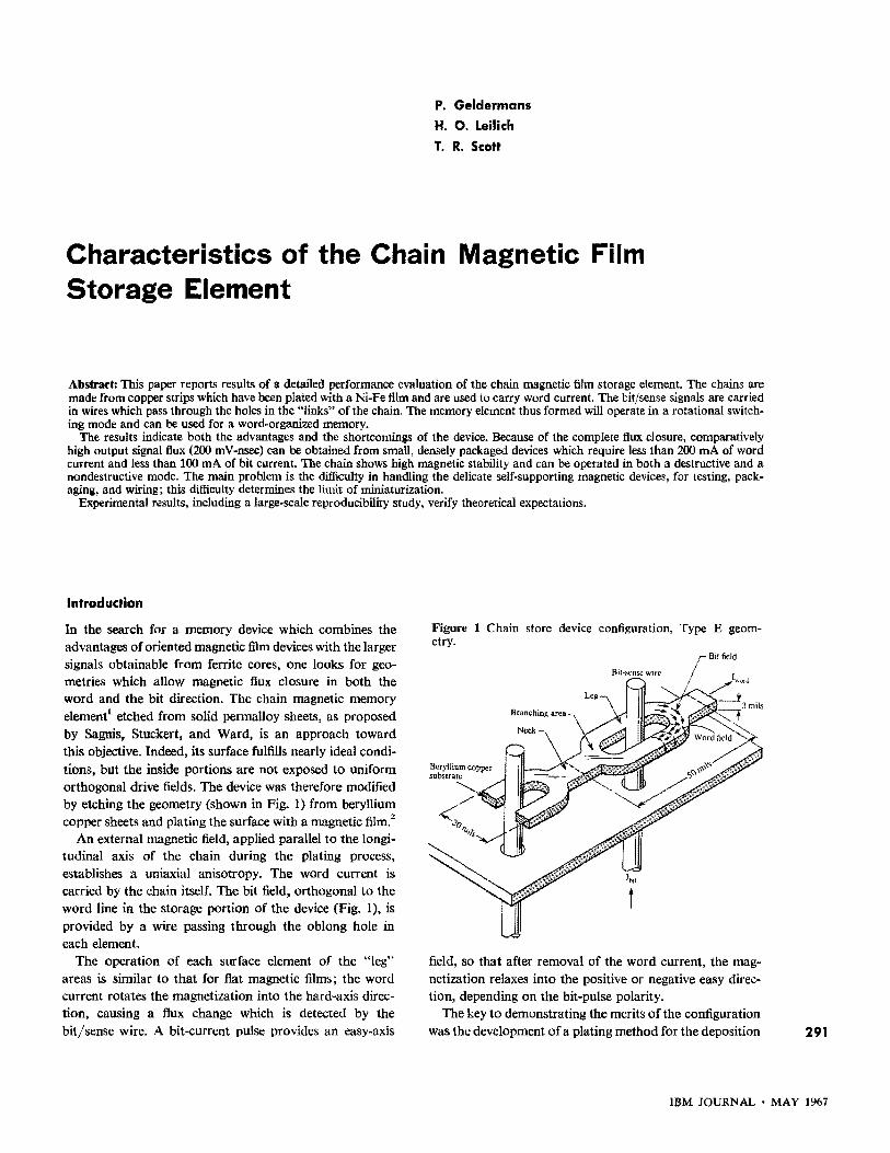
In the search for a memory device which combines theadvantages oforiented magnetic film devices with the largersignals obtainable from ferrite cores, one looks for geometries which allow magnetic flux closure in both theword and the bit direction. The chain magnetic memoryelement' etched from solid permalloy sheets, as proposed
by Sagnis, Stuckert, and Ward, is an approach towardthis objective. Indeed, its surface fulfills nearly ideal condi
tions, but the inside portions are not exposed to uniformorthogonal drive fields. The device was therefore modifiedby etching the geometry (shown in Fig. 1) from berylliumcopper sheets and plating the surface with a magnetic film,"
An external magnetic field, applied parallel to the longitudinal axis of the chain during the plating process,
establishes a uniaxial anisotropy. The word current iscarried by the chain itself. The bit field, orthogonal to theword line in the storage portion of the device (Fig. 1), is
provided by a wire passing through the oblong hole in
each element.The operation of each surface element of the "leg"
areas is similar to that for flat magnetic films; the wordcurrent rotates the magnetization into the hard-axis direction, causing a flux change which is detected by thebit/sense wire. A bit-current pulse provides an easy-axis
Figure 1 Chain store device configuration, Type E geometry.
BHfield
field, so that after removal of the word current, the mag
netization relaxes into the positive or negative easy direction, depending on the bit-pulse polarity.
The key to demonstrating the merits of the configurationwas the development of a plating method for the deposition 291
IBM JOURNAL' MAY 1967
292
(a)
(b)
(c)
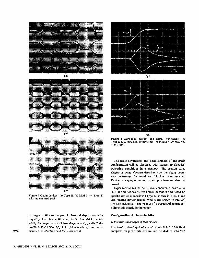
Figure 2 Chain devices: (a) Type E, (b) Mini-E, (c) Type Ewith interrupted neck.
of magnetic film on copper. A chemical deposition technique" yielded Ni-Fe films up to 30 kA thick, whichsatisfy the requirement of low dispersion (typically 2 degrees), a low anisotropy field (~ 4 oersteds), and sufficiently high coercive field (> 2 oersteds).
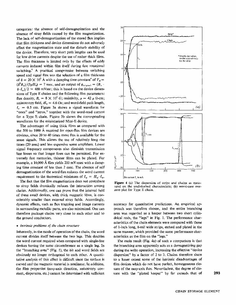
(aJ
(b)Figure 3 Word-read current and signal waveforms. (a)Type E (200 rnA/em. 10 mV/em); (b) Mini-E (100 rnA/em,4 mY/em).
The basic advantages and disadvantages of the chainconfiguration will be discussed with respect to electricaloperating conditions in a memory. The section titledChains as array elements describes how the chain geometry determines the word and bit line characteristics.Device packaging requirements and problems are also discussed.
Experimental results are given, concerning destructive(DRO) and nondestructive (NORO) modes and based onspecific device dimensions (Type E, shown in Figs. 1 and2a). Smaller devices (called Mini-E and shown in Fig. 2b)are also evaluated. The results of a successful reproducibility study conclude the paper.
Configurational characteristics
__ Intrinsic advantages of flux closure
The major advantages of chains which result from theircomplete magnetic flux closure can be divided into two
P. GELDERMANS, H. O. LEILICH AND T. R. SCOTT
Bit current Ih in rnA
293
Strip"
~ ( Chain~
")190%
"Double the valuesIbl on the vertical scale
for the strip
IJIIJ
~
f- k v
I I II (a)
0II
In,max!II
-10 I::: Ic I
~
c (b)eoU'i 20
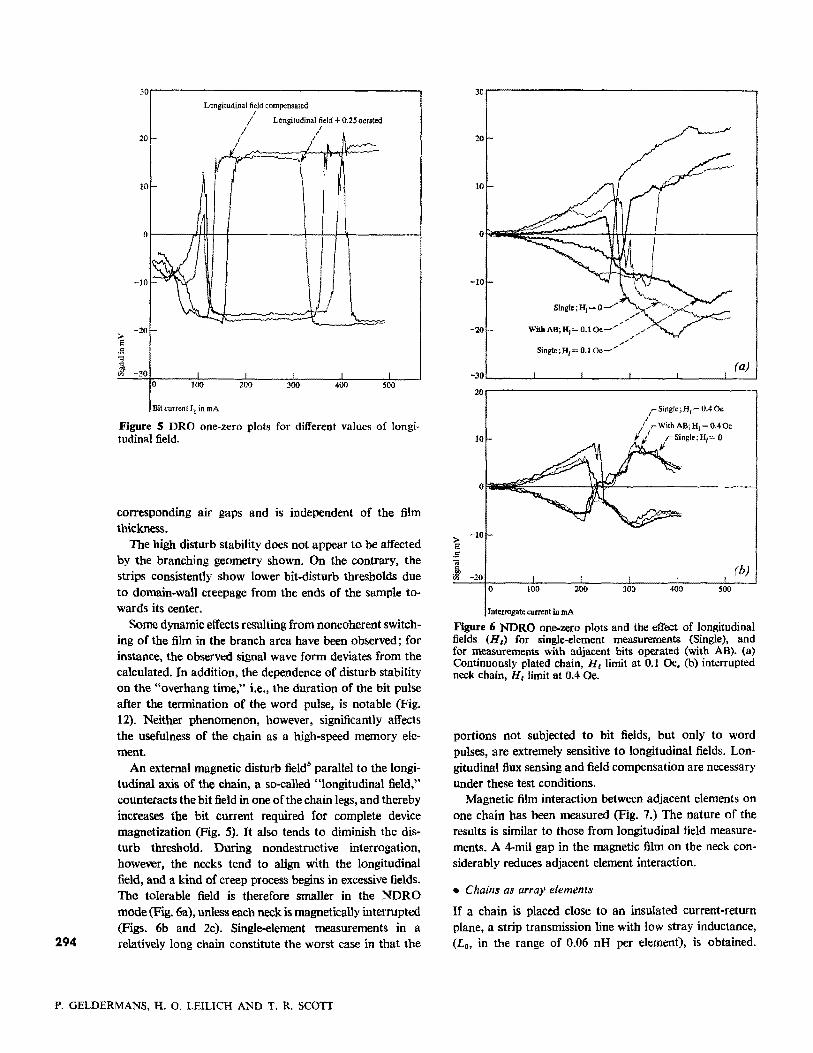
0 300
Figure 4 (a) The dispersion of strips and chains as measured on the undisturbed characteristic; (b) worst-case onezero plot for Type E chain.
10
30
-30
20r------------------------,
o
10
-20
20
-10
accuracy for quantitative predictions. An empirical approach was therefore chosen, and the entire branchingarea was regarded as a keeper between two short cylindrical rods, the "legs" in Fig. 1. The performance characteristics of the chain elements were compared with thoseof l-inch long, 8-mil wide strips, etched and plated in thesame manner, which provided the same performance characteristics as the film on the "legs."
The main result (Fig. 4a) of such a comparison is thatthe branching area apparently acts as a demagnetizing gapduring the write operation, increasing the effective "devicedispersion" by a factor of 2 to 3. Chains therefore shareto a lesser extent some of the intrinsic disadvantages offilm devices which do not have perfect, homogeneous closure of the easy-axis flux. Nevertheless, the degree of closure with the "plated keeper" by far exceeds that of
categories: the absence of self-demagnetization and theabsence of stray fields caused by the film magnetization.The lack of self-demagnetization of the stored flux impliesthat film thickness and device dimensions do not adverselyaffect the magnetization state and the disturb stability ofthe device. Therefore, very short path lengths can be usedfor low drive currents despite the use of rather thick films.The film thickness is limited only by the effects of eddycurrents induced within film itself during fast rotationalswitching," A practical compromise between switchingspeed and signal flux was the selection of a film thicknessof ij = 20 X 103 Awith a damping time constant4 of TE =(ij2B .}/ (3pH k ) = 7 nsec, and an output of cPsignsl = (B •.ij. f w }/ 2 = 400 mVsec; this is based on the device dimensions of Type E chains and the following film parameters:flux density, B. = 8 X 10³ G; resistivity, p = 42 IJ- Q-cm;anistotropy field, H k = 4.6 Oe; and word-field path length,f w = 0.5 em, Figure 3a shows a signal waveform for"ones" and "zeros," together with the word-read currentfor a Type E chain. Figure 3b shows the correspondingwaveforms for the miniaturized Mini-E device.
The advantages of using thick films as compared withthe 500 to 1000 Arequired for open-flux film devices areobvious, since 20 to 40 times more flux is available for thesense signals. This allows the use of relatively long risetimes (20 nsec) and less expensive sense amplifiers. Lowersignal frequency components also diminish transmissionline losses so that longer lines can be permitted. For extremely fast memories, thinner films can be plated. Forexample, a 10,000 A film yields 200 mV-nsec with a damping time constant of less than 2 nsec. The absence of selfdemagnetization of the word flux reduces the word currentrequirement to the theoretical minimum of L; = H w ' f w '
The fact that the film magnetization does not contributeto stray fields drastically reduces the interaction amongchains. Additionally, one can prove that the internal fieldof these small devices, with thick magnetic films, is considerably smaller than external stray fields. Accordingly,dynamic effects, such as flux trapping and image currentsin surrounding metallic parts, are also minimized. One cantherefore package chains very close to each other and tothe ground conductors.
• Intrinsic problems of the chain structure
Inherently, in the mode of operation of the chain, the wordcurrent divides itself between the two legs. This doublesthe word current required when compared with single-linedevices having the same circumference as a single leg. Inthe "branching area" (Fig. I), the bit and word fields areobviously no longer orthogonal to each other. A quantitative analysis of this effect is difficult since the surface iscurved and the magnetic material is nonlinear. In addition,the film properties (easy-axis direction, anisotropy constant, dispersion, etc.) cannot be determined with sufficient
CHAIN STORAGE ELEMENT
30r---------------------, 30,----------------------,
(a)
Single;H1=O-""
With Ali; H/= 0.1 oe-///::.///
Single;H/=O.10e-/
-301...-__...J-__-L__--l l.-__...l.-_-.J
20r---------------------,
-10
-20
10
20
Longitudinal field compensatedI
/ Longitudinal field +0.25 oerstedI I
I II I
{ {I I
20
10
;. -20
S.S-;;;
'"~ -300 100
,r Single;H, = 0.4 OeI
/ IrW;lh~B;H/=0.4Oe
,;t rSmgle;HI'~O
f-10
>e-10
.501
~ -20(b)
0
Interrogate current in rnA
Figure 6 NDRO one-zero plots and the effect of longitudinalfields (Hl ) for single-element measurements (Single), andfor measurements with adjacent bits operated (with AB). (a)Continuously plated chain, H, limit at 0.1 Oe, (b) interruptedneck chain, Hllimit at 0.4 Oe.
portions not subjected to bit fields, but only to wordpulses, are extremely sensitive to longitudinal fields. Longitudinal fluxsensingand fieldcompensation are necessaryunder these test conditions.
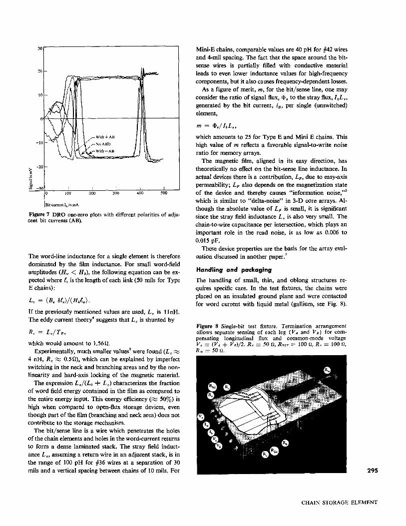
Magnetic film interaction between adjacent elements onone chain has been measured (Fig. 7.) The nature of theresults is similar to those from longitudinal field measurements. A 4-mil gap in the magnetic film on the neck considerably reduces adjacent element interaction.
• Chains as array elements
If a chain is placed close to an insulated current-returnplane, a strip transmission line with low stray inductance,(L n, in the range of 0.06 nB per element), is obtained.
BitcurrentIj, in mA
Figure 5 DRO one-zero plots for different values of longitudinal field.
corresponding air gaps and is independent of the filmthickness.
The high disturb stability does not appear to be affectedby the branching geometry shown. On the contrary, thestrips consistently show lower bit-disturb thresholds dueto domain-wall creepage from the ends of the sample towards its center.
Some dynamiceffectsresulting from noncoherent switching of the film in the branch area have been observed; forinstance, the ohserved signal wave form deviates from thecalculated. In addition, the dependence of disturb stabilityon the "overhang time," i.e., the duration of the bit pulseafter the termination of the word pulse, is notable (Fig.12). Neither phenomenon, however, significantly affectsthe usefulness of the chain as a high-speed memory element.
An external magnetic disturb fieldS parallel to the longitudinal axis of the chain, a so-called "longitudinal field,"counteracts the bit fieldin one of the chain legs,and therebyincreases the bit current required for complete devicemagnetization (Fig. 5). It also tends to diminish the disturb threshold. During nondestructive interrogation,however, the necks tend to align with the longitudinalfield, and a kind of creep process begins in excessive fields.The tolerable field is therefore smaller in the NDROmode (Fig. 00),unless each neck ismagnetically interrupted(Figs. 6b and 2c). Single-element measurements in arelatively long chain constitute the worst case in that the294
P. GELDERMANS, H. O. LEILICH AND T. R. SCOTT
295
Mini-E chains, comparable values are 40 pH for #42 wiresand 4-mil spacing. The fact that the space around the bitsense wires is partially filled with conductive materialleads to even lower inductance values for high-frequencycomponents, but it also causes frequency-dependent losses.
As a figure of merit, m, for the bit/sense line, one mayconsider the ratio of signal flux, <1>. to the stray flux, I bL.,generated by the bit current, iB , per single (unswitched)element,
Figure 8 Single-bit test fixture. Termination arrangementallows separate sensing of each leg (VA and VB) for compensating longitudinal flux and common-mode voltageVe = (VA + VB)/2. RA = 50 n, RBIT = 100 n, n, = 100 c,u; = 50 n,
m = <1>./ IbL.,
which amounts to 25 for Type E and Mini E chains. Thishigh value of m reflects a favorable signal-to-write noiseratio for memory arrays.
The magnetic film, aligned in its easy direction, hastheoretically no effect on the bit-sense line inductance. Inactual devices there is a contribution, LF , due to easy-axispermeability; LF also depends on the magnetization stateof the device and thereby causes "information noise.?"which is similar to "delta-noise" in 3-D core arrays. Although the absolute value of LF is small, it is significantsince the stray field inductance L. is also very small. Thechain-to-wire capacitance per intersection, which plays animportant role in the read noise, is as low as 0.006 to0.015 pF.
These device properties are the basis for the array evaluation discussed in another paper."
Handling and packaging
The handling of small, thin, and oblong structures requires specific care. In the test fixtures, the chains wereplaced on an insulated ground plane and were contactedfor word current with liquid metal (gallium, see Fig. 8).
~-20
.S-;;c
.9'-30'" 0 500
The word-line inductance for a single element is thereforedominated by the film inductance. For small word-fieldamplitudes tH; < H k), the following equation can be expected where te is the length of each link (50 mils for TypeE chains):
R, = Le/TE ,
which would amount to 1.560.Experimentally, much smaller values" were found tL; ~
4 nH, R, ~ 0.50), which can be explained by imperfectswitching in the neck and branching areas and by the nonlinearity and hard-axis locking of the magnetic material.
The expression LcI(Lo + L.) characterizes the fractionof word field energy contained in the film as compared tothe entire energy input. This energy efficiency (~ 50%) ishigh when compared to open-flux storage devices, eventhough part of the film (branching and neck area) does notcontribute to the storage mechanism.
The bit/sense line is a wire which penetrates the holesof the chain elements and holes in the word-current returnsto form a dense laminated stack. The stray field inductance L., assuming a return wire in an adjacent stack, is inthe range of 100 pH for #36 wires at a separation of 30mils and a vertical spacing between chains of 10 mils. For
If the previously mentioned values are used, L, is llnH.The eddy current theory" suggests that L; is shunted by
30
20
Bit current lb in rnA
Figure 7 DRO one-zero plots with different polarities of adjacent bit currents (AD).
CHAIN STORAGE ELEMENT
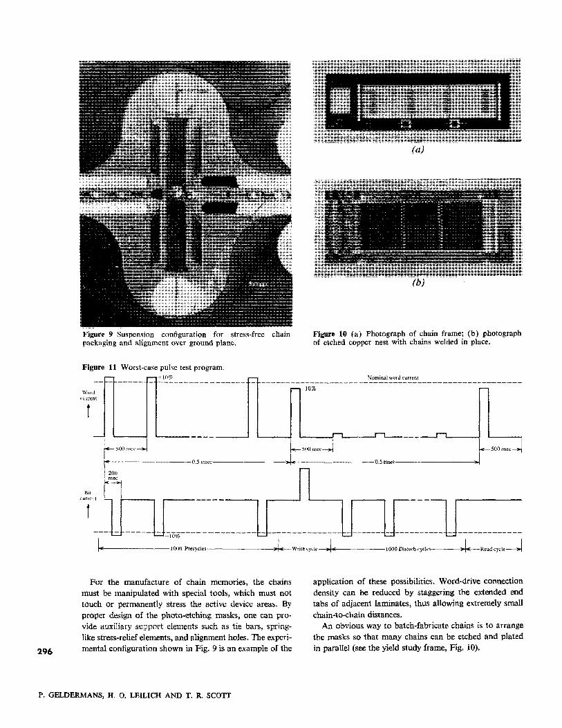
Figure 9 Suspension configuration for stress-free chainpackaging and alignment over ground plane.
(aJ
Figure 10 (a) Photograph of chain frame; (b) photographof etched copper nest with chains welded in place.
Figure 11 Worst-case pulse test program.+10% Nominal word current
Wordcurrent
-10%
1
Lsoonsec-l
"I(j,5rnsec---------:>ot"!----------O.'imsec--------;*"--------
Bjlcurrent
1---4-~-----~-+·--·---------------- - -------------- ------ - -------~-------------1+--------1000 preCYC1e'--------7"tJl'f...--WrireCYcle--!.--.----IOOO Disturb<Y<ks,---....»~Read CYcle~
296
For the manufacture of chain memories, the chainsmust be manipulated with special tools, which must nottouch or permanently stress the active device areas. By
proper design of the photo-etching masks, one can provide auxiliary support elements such as tie bars, springlike stress-relief elements, and alignment holes. The experimental configuration shown in Fig. 9 is an example of the
application of these possibilities. Word-drive connectiondensity can be reduced by staggering the extended endtabs of adjacent laminates, thus allowing extremely smallchain-to-chain distances.
An obvious way to batch-fabricate chains is to arrangethe masks so that many chains can be etched and platedin parallel (see the yield study frame, Fig. 10).
P. GELDERMANS, H. O. LElLICH AND T. R. SCOTT
_I
_I
I... To=70nsec ~l(aJ
(b) -J LTo = 17nsec
600
(c)QII
500II
To=70nsec\q\\\\
400\
~,,\b,
1 ""300 ........
.S ....--0
..:r-aE~ 200
0 300 400
Bit current Ib in rnA
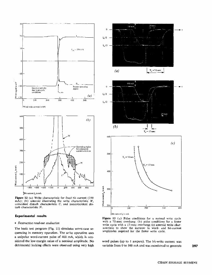
Figure 12 (a) Write characteristic for fixed bit current (250rnA); (b) asteroid illustrating the write characteristic W,coincident disturb characteristic C, and noncoincident disturb characteristic N.
600
(b)
500
I,I
400 V w
I
'I Operating regionfor coincident
300 current selection
I
200 I-ea.S ·/v.....c 100
~ ..:~G1!~ 0
30
20 - I
rr"10- Ibit=250mA
0
-10 -
> 0E
tc -20 Proper operating~
Inverted polarity region.~
due to precyclcIw,minconditions
II(a)~ -30 I I I
0 100 200 300 400 500
Word write current in rnA
Experimental results
• Destructive read-out evaluation
The basic test program (Fig. 11) simulates worst-case sequencing in memory operation. The write operation usesa unipolar word-current pulse of 400 rnA, which is considered the low-margin value of a nominal amplitude. Nodetrimental locking effects were observed using very high
Bit current IIIin rnA
Figure 13 (a) Pulse conditions for a normal write cyclewith a 70-nsec overhang; (b) pulse conditions for a fasterwrite cycle with a 17-nsec overhang; (c) asteroid write characteristic to show the increase in word- and bit-currentamplitudes required for the faster write cycle.
word pulses (up to 1 ampere). The bit-write current wasvariable from 0 to 500 rnA and was monitored to generate 297
CHAIN STORAGE ELEMENT
v. t
(b)
Figure 14 (a) Pulse conditions for a fast write cycle; (b) associated signal for a separate read pulse.
r--------------------,sooo PositivesignalA Negative signal
Figure 15 The effect of longitudinal stress on the signalamplitude and minimum and maximum bit currents.
10% higher than the nominal value while the word-writecurrent is 10% lower. Their ratio (1.22) is maintained overthe entire plot.
The disturb phase consists of 1000 bit pulses at 110% ofthe nominal value in the opposite direction coincident withword-disturb currents of 30 rnA amplitude, which corresponds to about 10% of H k and represents possibleleakage current in nonselected word lines.
The word-read current used is similar to the wordwrite current, and is shown in Fig. 3a, together with thesignal waveform.
For bit current values up to I bb the undisturbed outputsignal increases and the magnetization state proves to bevery disturb-sensitive, The dispersion" can be read fromFig. 4a to be
agO device = (Ibltu,)/(htb) ~ 5.7 0,
using the path lengths t .. = 20 mils and t b = 80 mils. Thisis the effective device dispersion under application-typetest conditions and includes device configuration effects.The "film dispersion" measured on strips under the sameconditions is about 2° (see Fig. 4a and the discussionabove).
The device becomes magnetically stable when the bitcurrent exceeds I b min as shown by the constant amplitude of V. in Fig. 4b. I bmo% is the wall-motion threshold;22% higher values are allowed since this margin is incorporated in the test.
A plot of the amplitude of the word-write current shows(Fig. 12a) a similarly sharp threshold I w m i n , while lowercurrents have no effect upon the magnetization which hasbeen previously fixed in the opposite direction.
Plotting I; min versus I b min (Fig. 12b, trace a) producesa very useful graph which corresponds to Stoner-Wohlfarth's "asteroid" presentation of switching threshold. This
400
30020r - - -o-__--<)- _v,
200
Ib,min
10
100
:e ~.S .S~' 0 0 ..:f'
0 ]0 20 30
F(g)
the horizontal axis of the plot (Fig. 4b). The timing ofword and bit pulses is shown in Fig. 13a.
Prior to the write operation, the device was conditionedby 1000 precycles. These are orthogonal-mode write operations with inverse bit currents which firmly magnetizethe device in the opposite direction. These bit currents are298
P. GELDERMANS, H. O. LEIUCH AND T. R. SCOTT
asteroid relates actual device properties under worst-caseapplication conditions. Also included in Fig. 12b are thethresholds for combinations of 1000 word- and bit-disturbpulses which in coincidence (trace b) and alternating noncoincidence (trace c) will destroy 10% of the written information. This gives the wall-motion threshold for thedestructive read, nondestructive read, and coincident-current selection modes of operation (see next section). Forthese types of films, the wall motion threshold does notchange as the number of disturb pulses increases (up tolOll). It has been verified that the signal waveforms areidentical in all details if the peak voltages are equal.
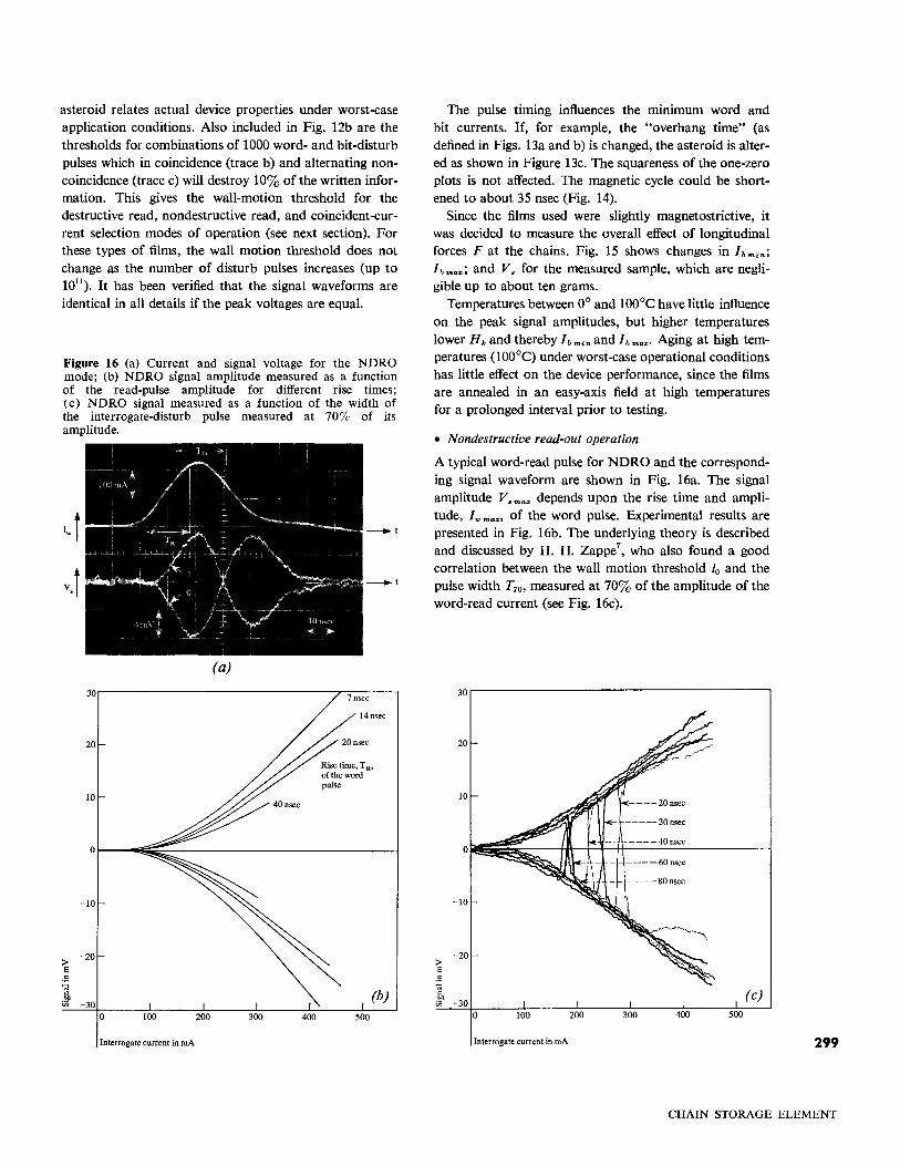
Figure 16 (a) Current and signal voltage for the NDROmode; (b) NDRO signal amplitude measured as a functionof the read-pulse amplitude for different rise times;(c) NDRO signal measured as a function of the width ofthe interrogate-disturb pulse measured at 70% of itsamplitude.
_I
_I
(a)
30r-----------------r-::------,
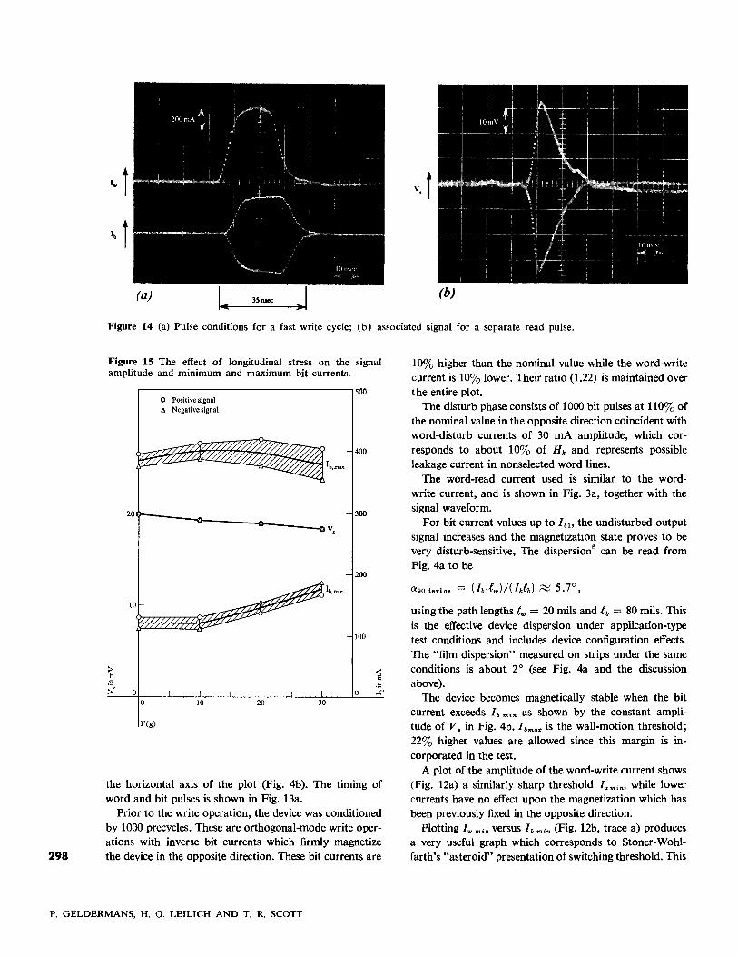
The pulse timing influences the rmrnmum word andbit currents. If, for example, the "overhang time" (asdefined in Figs. 13a and b) is changed, the asteroid is altered as shown in Figure Bc. The squareness of the one-zeroplots is not affected. The magnetic cycle could be shortened to about 35 nsec (Fig. 14).
Since the films used were slightly magnetostrictive, itwas decided to measure the overall effect of longitudinalforces F at the chains. Fig. 15 shows changes in lbmin;
I b ma.; and V. for the measured sample, which are negligible up to about ten grams.
Temperatures between 0° and 100°C have little influenceon the peak signal amplitudes, but higher temperatureslower H k and thereby I b min and I b ma.' Aging at high temperatures (l00°C) under worst-case operational conditionshas little effect on the device performance, since the filmsare annealed in an easy-axis field at high temperaturesfor a prolonged interval prior to testing.
• Nondestructive read-out operation
A typical word-read pulse for NDRO and the corresponding signal waveform are shown in Fig. 16a. The signalamplitude V. max depends upon the rise time and amplitude, lw ma.. of the word pulse. Experimental results arepresented in Fig. 16b. The underlying theory is describedand discussed by H. H. Zappe", who also found a goodcorrelation between the wall motion threshold io and thepulse width T70 , measured at 70% of the amplitude of theword-read current (see Fig. 16c).
30r------------------------,
14nsec
20
10
°t--_iJiiii~--------------___j
-10
-20 -20
~ >s.S .S
" " (c)c (b) c
~ .!!' -30-30 <n
0 0 500
Interrogate currentin rnA Interrogate current in rnA 299
CHAIN STORAGE ELEMENT
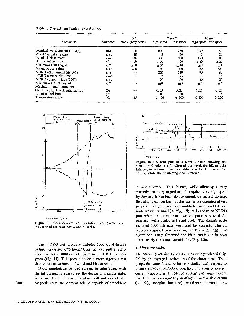
Table 1 Typical application specifications
Yield Type-E Mini-EParameter Dimension study specification high-speed low-speed high-speed low-speed
Nominal word current (±10%) mA 700 600 450 240 180Wordcurrent rise time nsee 20 5 20 5 20Nominal bit current mA 176 300 200 150 100Bitcurrent margins g~ ±1O ±20 ±20 ±20 ±20Minimum DRO signal mV ±1O ±20 ±10 ±8 ±4Magnetic cycle time nsee 200 40 200 40 200NDRO read current (±10%) rnA 220 220 90 90NDRO current rise time nsee 7 15 7 15NDRD current width (70%) nsee 20 20 20 20MinimumNDRO signal mV ±8 ±5 ±3 ±2Maximum longitudinal field(DRO, without neck interruption) Oe 0.25 0.25 0.25 0.25Longitudinal force gm 10 10 3 3Temperaturerange °C 25 0-100 0-100 0-100 0-100
po
Figure 18 One-zero plot of a Mini-E chain showing thesignal amplitude as a function of the word, the bit, and theinterrogate current. Two variables are fixed at indicatedvalues, while the remaining one is varied.
20
lO:;r~l!£""'~"..~ ~
~I/lint. disturbrv
0
~ 1\ rvW>- IbjtwriteS ---E -10 t tgr1 -20 I , I I I I
-400 -300 -200 -100 0 100 200 300 400 500
Milliam res
Inverse polarityProper polarity ~~~to destructive
Inverse polaritydue to insufficientwrite
20
30
10
O!"-"""==-------t+--,-+-+----------l
40r-------------------~
-10
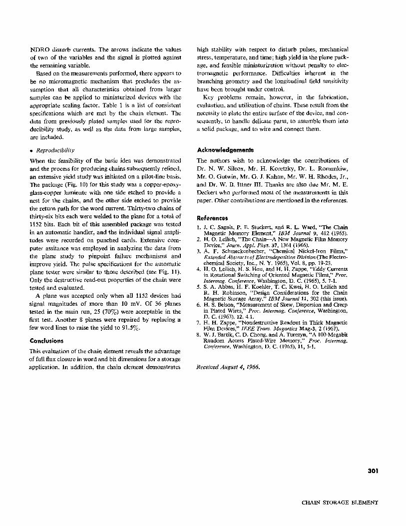
Figure 17 Coincident-current operation plot (same wordpulsesused for read, write, and disturb).
;;. -20Ei.S]Jf -30
o
Word current Iw in mA
1",=280mA±5%Ib=350mA±5%
current selection. This feature, while allowing a veryattractive memory organization", requires very high quality devices. It has been demonstrated, on several devices,that chains can perform in this way in an operational testprogram, yet the margins allowable for word and bit currents are rather small (± 5%). Figure 17 shows an NDROplot where the same word-current pulse was used forprecycle, write cycle, and read cycle. The disturb cycleincluded 1000 alternate word and bit currents. The bitcurrents required were very high (350 mA ± 5%). Theoperational range for word and bit currents can be seenquite clearly from the asteroid plot (Fig. 12b).
300
The NDRO test program includes 1000 word-disturbpulses, which are 22% higher than the read pulses, interleaved with the 1000 disturb cycles in the DRO test program (Fig. 11). This proved to be a more rigorous testthan consecutive bursts of word and bit currents.
If the nondestructive read current in coincidence withthe bit current is able to set the device in a stable state,while word and bit currents alone will not disturb themagnetic state, the element will be capable of coincident
• Miniature chains
The Mini-E (half-size Type E) chains were produced (Fig.2b) by photographic reduction of the chain mask. Theirproperties were found to be very similar with respect todisturb stability, NDRO properties, and even coincidentcurrent capabilities at reduced current and signal levels.Fig. 18 shows a composite plot of signal versus bit currents(± 20% margins included), word-write current, and
P. GELDERMANS, H. O. LEILICH AND T. R. SCOTT
NORO disturb currents. The arrows indicate the valuesof two of the variables and the signal is plotted againstthe remaining variable.
Based on the measurements performed, there appears tobe no micromagnetic mechanism that precludes the assumption that all characteristics obtained from largersamples can be applied to miniaturized devices with theappropriate scaling factor. Table 1 is a list of consistentspecifications which are met by the chain element. Thedata from previously plated samples used for the reproducibility study, as well as the data from large samples,are included.
• Reproducibility
When the feasibility of the basic idea was demonstratedand the process for producing chains subsequently refined,an extensive yield study was initiated on a pilot-line basis.The package (Fig. 10) for this study was a copper-epoxyglass-copper laminate with one side etched to provide anest for the chains, and the other side etched to providethe return path for the word current. Thirty-two chains ofthirty-six bits each were welded to the plane for a total of1152 bits. Each bit of this assembled package was testedin an automatic handler, and the individual signal amplitudes were recorded on punched cards. Extensive computer assitanee was employed in analyzing the data fromthe plane study to pinpoint failure mechanisms andimprove yield. The pulse specifications for the automaticplane tester were similar to those described (see Fig. 11).Only the destructive read-out properties of the chain weretested and evaluated.
A plane was accepted only when all 1152 devices hadsignal magnitudes of more than 10 mY. Of 36 planestested in the main run, 25 (70%) were acceptable in thefirst test. Another 8 planes were repaired by replacing afew word lines to raise the yield to 91.5%.
Conclusions
This evaluation of the chain element reveals the advantageof full flux closure in word and bit dimensions for a storageapplication. In addition, the chain element demonstrates
high stability with respect to disturb pulses, mechanicalstress, temperature, and time; high yield in the plane package, and feasible miniaturization without penalty to electromagnetic performance. Difficulties inherent in thebranching geometry and the longitudinal field sensitivityhave been brought under control.
Key problems remain, however, in the fabrication,evaluation, and utilization of chains. These result from thenecessity to plate the entire surface of the device, and consequently, to handle delicate parts, to assemble them intoa solid package, and to wire and connect them.
Acknowledgements
The authors wish to acknowledge the contributions ofDr. N. W. Silcox, Mr. H. Koretzky, Dr. L. Romankiw,Mr. O. Gutwin, Mr. G. J. Kahan, Mr. W. H. Rhodes, Jr.,and Dr. W. B. Ittner III. Thanks are also due Mr. M. E.Deckert who performed most of the measurements in thispaper. Other contributions are mentioned in the references.
References
1. J. C. Sagnls, P. E. Stuckert, and R. L. Ward, "The ChainMagnetic Memory Element," IBM Journal 9, 412 (1965).
2. H. O. Leilich,"The Chain-A New Magnetic Film MemoryDevice," Journ. Appl. Phys. 37, 1361 (1966).
3. A. F. Sehmeckenbecher, "Chemical Nickel-Iron Films,"Extended Abstracts of Electrodeposition Division (The Electrochemical Society, Inc., N. Y. 1965), Vol. 8, pp. 19-23.
4. H. O. Leilich,H. S. Hou, and H. H. Zappe, "Eddy Currentsin Rotational Switchingof Oriented Magnetic Films," Proc.Intermag, Conference, Washington, D. C. (1965), 5. 7-1.
5. S. A. Abbas, H. F. Koehler, T. C. Kwei, H. O. Leilich andR. H. Robinson, "Design Considerations for the ChainMagnetic Storage Array," IBM Journal 11, 302 (this issue).
6. H. S. Belson,"Measurement of Skew, Dispersion and Creepin Plated Wires," Proc. lntermag, Conference, Washington,D. C. (1963), 12, 4.1.
7. H. H. Zappe, "Nondestructive Readout in Thick MagneticFilm Devices," IEEE Trans. Magnetics Mag-3, 2 (1967).
8. W. J. Bartik, C. D. Chong, and A. Turczyn,"A loo-MegabitRandom Access Plated-Wire Memory," Proc. Intermag,Conference, Washington, D. C. (1965), 11, 5-1.
Received August 4, 1966.
301
CHAIN STORAGE ELEMENT