charging and defects in single-walled carbon …
TRANSCRIPT

CHARGING AND DEFECTS IN SINGLE-WALLED CARBON NANOTUBES
BY
KHOI THI NGUYEN
DISSERTATION
Submitted in partial fulfillment of the requirements for the degree of Doctor of Philosophy in Materials Science and Engineering
in the Graduate College of the University of Illinois at Urbana-Champaign, 2011
Urbana, Illinois
Doctoral Committee
Associate Professor Moonsub Shim, Chair Professor John Abelson Professor Joseph Lyding Professor Angus Rockett

ABSTRACT
Single-Walled Carbon Nanotubes (SWCNTs) have been one of the most
intensively studied materials. Because of their single-atomic-layer structure, SWCNTs
are extremely sensitive to environmental interactions, in which charge transfer and defect
formation are the most notable effects. Among a number of microscopic and
spectroscopic methods, Raman spectroscopy is a widely used technique to characterize
physics and chemistry of CNTs. By utilizing simultaneous Raman and electron transport
measurements along with polymer electrolyte gating, this dissertation focuses on studying
charging and defects in SWCNTs at single nanotube level and in single layer graphene,
the building block of SWCNTs.
By controllably charging metallic SWCNTs (m-CNTs), the intrinsic nature of the
broad and asymmetric Fano lineshape in Raman G band of m-CNTs was first time
evidenced. The observation that Fano component is most broadened and downshifted
when Fermi level is close to the Dirac point (DP) reveals its origin as the consequence of
coupling of phonon to vertical electronic transitions. Furthermore, we have systematically
introduced covalent defects to m-CNTs to study how phonon softening and electrical
characteristics are affected by disorders. In addition to decreasing electrical conductance
with increasing on/off current ratio eventually leading to semiconducting behavior,
adding covalent defects reduces the degree of softening and broadening of longitudinal
optical (LO) phonon mode but enhances the softening of transverse optical (TO) mode of
the G-band near the DP. Charging and defect effects in semiconducting SWCNTs and
single layer graphene, a closely related material to SWCNTs, have also been discussed.
ii

To my Mother
iii

ACKNOWLEDGMENTS
First and foremost, I would like to sincerely thank my advisor, Professor
Moonsub Shim, for his guidance during my PhD research and study. I am grateful for his
patience, enthusiasm, and expectations, which partially motivated me to develop an
understanding of the subject. He has influenced how I think about doing research and
teaching. I am thankful to him for many discussions which have helped me to shape and
refine my views. If my words of thanks seem short, my gratitude to him is long and deep.
I would like to thank my committee members: Prof. John Abelson, Prof. Joseph
Lyding, and Prof. Angus Rocket, for their helpful comments and hard questions. In
particular, I am grateful to Prof. John Abelson for enjoyable conversations I have had
with him, for his career suggestions and encouragement.
My thanks go to my former and current labmates: Taner Ozel, Kwan-Wook Won,
JueHee Back, Anshu Gaur, Johnathon Tsai, Hunter McDaniel, and Daner Abdula, for
helping me in experiments, for stimulating discussions, and all the fun we have had in the
past few years. I especially thank Taner Ozel for his friendship and helping me get
through difficult times even after he graduated, and Daner Abdula for his support and
intensity which have inspired confidence in me.
Ken and Mary Jo Rott have been constant source of encouragement to me. They
are like my spiritual grandparents who keep my belief in kindness and love. I am
indebted to them for making a home away from home for me.
iv

I am heartily thankful to my best friend, Lan Anh Tran, for always being available
to share with me happiness as well as sadness, for her care, and for her desire of having
me back when I am far away. I should thank our destiny of letting us grow up together.
Most importantly, I wish to thank my parents. I have been lucky to have my
mother at my side whose support, encouragement and love made all the difference in the
world. She often makes me look better than I am. To her I dedicate this dissertation.
Finally, I would like to thank National Science Foundation, Department of
Materials Science and Engineering, and Vietnam Education Foundation for their financial
support.
v

TABLE OF CONTENTS CHAPTER 1: CARBON NANOTUBES: BASICS, SYNTHESIS, AND
METROLOGY… ........................................................................................1 1.1. Introduction ...............................................................................................................1
1.2. Single-Walled Carbon Nanotube Metrology.............................................................2
1.3. Synthesis, Field Effect Transistor Fabrication and Characterization........................8
1.4. References ...............................................................................................................11
1.5. Figures.....................................................................................................................14
CHAPTER 2: CHARGING TO ELUCIDATE ELECTRON-PHONON COUPLING IN METALLIC CARBON NANOTUBES ..............................................26
2.1. Introduction .............................................................................................................26
2.2. Fano Lineshape and Kohn Anomaly.......................................................................27
2.3. Physics of Raman Fano Component .......................................................................30
2.4. References ...............................................................................................................34
2.5. Figures.....................................................................................................................37
CHAPTER 3: DEFECTS IN METALLIC CARBON NANOTUBES ............................45 3.1. Charging, Defect, and Defect Characterization.......................................................45
3.2. Covalent Defect Introduction to Metallic Nanotubes..............................................47
3.3. References ...............................................................................................................54
3.4. Figures.....................................................................................................................56
CHAPTER 4: CHARGING AND DEFECTS IN SEMICONDUCTING CARBON NANOTUBES ..........................................................................................63
4.1. Doping Dependence of Raman G-band ..................................................................63
4.2. Line Broadening and Blueshift upon Covalent Defect Formation..........................66
4.3. References ...............................................................................................................68
4.4. Figures.....................................................................................................................70
CHAPTER 5: DOPING GRAPHENE...............................................................................77 5.1. Chemical Doping with 4-Bromobenzenediazonium Tetrafluoroborate..................78
5.2. Doping and Temperature Dependence....................................................................80
5.3. Conclusion...............................................................................................................85
5.4. References ...............................................................................................................86
5.5. Figures.....................................................................................................................89
CHAPTER 6: CONCLUSIONS ......................................................................................101
vi
CHAPTER 1
CARBON NANOTUBES BASICS, SYNTHESIS, AND METROLOGY
1.1. Introduction
Since their discovery in 1991, carbon nanotubes (CNTs) have been one of the
most intensively studied materials and have kept intriguing both scientists and engineers
in the last two decades. The number of publications on CNTs keeps increasing as shown
in figure 1.1 [1] and it sets CNTs apart from other research areas that appear ideal at the
beginning, for example, high temperature superconductivity. The reason for that unusual
continuing vitality is the unique combination of exceptional properties of CNTs. First,
CNTs are two order of magnitude stronger than steel at 1/6th of the weight. CNTs are
also excellent conductors of heat [2]. Moreover, CNTs offer extremely high carrier
mobility, up to 105 cm2/V.s, two orders of magnitude higher than current silicon
electronics. In addition, CNTs appear to be biocompatible in many environments [3].
Thanks to an amazing combination of properties, CNTs appear to be ideal for a
wide range of applications, including molecular electronics, quantum computing,
materials science, and medicine. Electronic applications of CNTs grab most of media
limelight because of the thrust for smaller and faster devices. Electron-phonon coupling
is particularly important for transport properties in CNTs, as it is ultimate limiting factor
of high-filed carrier mobility [4, 5, 6]. Therefore, electron-phonon coupling, which can
be quantified via phonon frequency, linewidth, and intensity measured by Raman
spectroscopy, is important to understand for both CNT applications and fundamental
sciences. This thesis focuses on studying electron-phonon coupling in single-walled
1

CNTs (SWCNTs) under charging and defects by utilizing simultaneous Raman and
transport measurements, and polymer electrolyte gating.
SWCNTs can be considered as one atom thick graphene sheet rolled up into
seamless tubes, one atom thick, along chiral vector Ch, as indicated in figure 1.2. Chiral
vector is described by Ch = na1+ma2 where a1 and a2 are unit vectors of the hexagonal
lattice; n and m are integer, 0≤m≤n, and are called chiral indices. Each SWCNT is
characterized by a pair of n and m, as (n,m). They are called armchair if m=n, zigzag if
m=0, and chiral nanotubes in all other cases.
The electronic properties of SWCNTs depend on n and m. They are metallic
nanotubes (m-CNTs) if the difference between n and m is a multiple of three (though
only armchair nanotubes are truly metallic) and semiconducting nanotubes (s-CNTs)
otherwise [2]. For m-CNTs, the valence and conduction bands touch each other at a
single point, Dirac point (DP), as shown in figure 1.3b, which is not the case for s-CNTs
where a diameter dependent bandgap of about 0.5 eV is formed as indicated in figure
1.3a. Of particular interest is the density of states (DOS) of SWCNTs with the appearance
of van Hove singularities (vHs) as expected for 1D materials. A finite DOS between the
first two vHs of m-CNTs distinguishes them from s-CNTs (figures 1.3c and 1.3d). These
characteristics play a crucial role in understanding many physical as well as chemical
properties of CNTs, and some of them will be described in the following.
1.2. Single-Walled Carbon Nanotube Metrology
The existence of SWCNTs and their properties are evidenced and investigated by
several techniques, for instance, electron microscopy, scanning probe microscopy, and
optical techniques. While each method has both advantages and disadvantages,
2

combinations of techniques give us a comprehensive picture of SWCNT characteristics
and potential applications. Methods that are used to characterize SWCNTs in this work
are briefly summarized below.
1.2.1. Atomic Force Microscopy
In atomic force microscopy (AFM), a sharp tip in the shape of a pyramid moves
over the contours of the surface, at near-atomic precision, and as it does so, the cantilever
at the back of the tip moves up and down. This motion is detected using the deflection of
a laser beam, which bounces off the back of the cantilever, and thus a map of any surface
is obtained, at a resolution of less than 1nm vertically. There are different modes - contact
mode, in which the tip is scraping across the surface, noncontact mode or tapping mode,
in which the tip vibrates up and down, and responds to the proximity of the surface,
without actually touching it, and ultrasonic mode, or UFM, in which the sample is
vibrated at very high frequencies (1-2 MHz), which causes the tip to sense the relative
softness of various features on the surface in addition to a high resolution.
In our work, we use tapping mode to image CNTs on silicon substrate with 300 nm thick
SiO2 oxide layer in order to check the number of CNTs in the channel of devices and to
see if tube of interest are isolated as well as nanotube diameter. An AFM image of a
single connection CNT-based FET is shown in figure 1.12.
1.2.2. Electrical Measurement
Electrical measurements of individual SWCNTs have proven to be a powerful
probe of this novel 1D system. Figure 1.4 shows a schematic of commonly used device
geometry. A SWCNT is connected to two metallic contacts, source and drain electrodes,
3

and capacitively coupled to the third electrode that is used to change charge density, or,
in other words, control the Fermi level, in the SWCNT. This three-terminal geometry has
been used to address both device performance and fundamental physics [7].
The transport properties of SWCNTs are directly related to their electronic
structure. Transconductance measurement is a means to distinguish s-CNTs and m-CNTs
as indicated in figure 1.5. Semiconducting SWCNT exhibits a broad range of zero-
conductance because of Fermi level tuned into bandgap while m-CNT shows slight gate
dependence as Fermi level reaches the first vHs. Conductance depends also on contact
resistance and carrier scattering rate. For the former, Au and Pd have proven to make the
best contacts (Ohmic) to CNTs with nearly perfect transmission [8]. For the latter, defect
scattering and electron-phonon coupling are dominant mechanisms [4, 5, 6, 9, 10]
There are several sources of disorders in CNTs. The first one is localized lattice
defects, such as vacancies, substitutions, and pentagon-heptagon defects. Such defects are
typically formed during nanotube growth or by intentional damage [9]. The second
source is electrostatic potential fluctuations, created by contaminants or trapped charges
in the substrate, or by adsorbed molecules. The third one is mechanical deformations, for
instance, strain, twist and kinks [10]. The presence of these defects reduces the
transmission coefficient of carrier transport [9, 10].
In clean, high-quality m-CNTs at room temperature, the dominant scattering
mechanism is well known to be electron-phonon scattering [4, 5, 6, 11]. Scattering by
acoustic phonons dominates the resistance at low source-drain bias [11], whereas
scattering by optical and zone boundary phonons sets a limit on maximum current carried
out by individual CNT at high bias [4, 5, 6]. The latter is shown in figure 1.6 for a m-
4

CNT. The slope of current-voltage curve decreases for increasing bias, and can even
become negative for suspended CNT. This is explained by phonon emission by electrons
as soon as they gain energy equal to optical phonon energy, ~0.16eV. The energy created
by phonon emission can heat CNT significantly, particularly for suspended tubes, which
are not supported by substrate for heat dissipation, and can lead to negative differential
resistance [12].
Phonon scattering also limit the ultimate performance of s-CNT devices as shown
in figure 1.7 for temperature dependence of the linear conductance of such a device [13].
The on-state resistance increases linearly with temperature, indicative of scattering by
acoustic phonons, whose occupation also grows linearly with temperature.
1.2.3. Raman Spectroscopy
Raman spectroscopy is one of the most sensitive, easy-to-use, and powerful
techniques in characterizing CNTs. It can be performed on both bundled and single
CNTs, and carried out at room temperature and ambient pressure. Raman spectroscopy
has been used to characterize SWCNTs for many different purposes, from synthesis and
purification process all the way to nanotube modifications and device applications. This
section presents an overview of Raman spectroscopy in SWCNTs.
Raman scattering is an inelastic scattering of photons. Through phonon excitation
(or relaxation), scattered photon loses (or gains) the characteristic energy of phonon
relative to energy of incident photon. A schematic Raman scattering is shown in figure
1.8. Raman spectra refer to the spectral intensity of scattered photon as a function of
energy shift, or phonon energy. The photon scattering process generally occurs even
without support of electronic structure which would correspond to a nonresonant process
5

with weak Raman signal. However, thanks to the resonance of incident or scattered
photons with an optical transition between vHs (e.g., E11 as shown in figure 1.3d) of this
1-D material, scattering amplitude becomes large, and makes the observation of Raman
signal from CNTs at single tube level possible. Figure 1.9 gives examples of Raman
spectra from an individual CNT with four prominent features: Radial breathing mode
(RBM), defect-related D-band and its overtone 2D band, and tangential mode (or G-
band). The importance of these Raman modes is discussed in detail below.
• Radial Breathing Mode (RBM)
RBM is one signature that distinguishes CNT from other forms of graphitic
materials. RBM corresponds to the symmetric in-phase displacements of all carbon atoms
in CNT in the radial direction, with frequency in the range 100-350 cm-1. As expected,
RBM frequency is proportional to reciprocal of nanotube diameter [14] and usually used
to determine nanotube chirality as indicated in figure 1.10, the Kataura plot. Each point
corresponds to an optical transition with a specific chirality (n, m) [15, 16]. Since
Kataura plot is based on one electron electronic structure which does not take into
account electron-electron interaction, electron-phonon interaction, or interaction between
CNT and its surroundings, the plot can serve as a rough reference.
• Tangential Mode
The multiple-feature Raman G-band is another important characteristic of CNTs.
The optical phonon G mode arises from the tangential vibration of carbon atoms in the
range 1500-1630 cm-1. It corresponds to the in-plane E2g optical phonon mode in the
parent graphene. Since unit cell of graphene consists of two equivalent atoms, the
6

longitudinal (LO) and transverse (TO) optical modes are degenerate at zone center of the
Brillouin zone. When graphene is rolled up to form a SWCNT, due to the radial
confinement and curvature of cylindrical shape, the degeneracy is removed, and G-band
mainly splits into two features, G+ and G-, in which G- mode has lower frequency. For s-
CNTs, G+ corresponds to the LO mode, and G- to the TO mode, which is softened due to
the mixing of sp2 and sp3 bond characteristics induced by curvature effects [17] Both
narrow and symmetric G+ and G- peaks can be well fitted by Lorentzian function. For m-
CNTs, while G+ has narrow Lorentzian lineshape G- shows either Lorentzian or
asymmetric and broad Fano lineshape which is represented by Breit-Wigner-Fano line
shape: ( ) ( )[ ]( )[ ]2
0
20
0 /1/1
Γ−+Γ−+
=ωω
ωωω
qII where ω0, I0 and Γ is frequency, intensity, and
broadening parameter, respectively, 1/q is a measure of the interaction of phonon with a
continuum of states [18] These have been debates in whether Fano lineshape is intrinsic
property of metallic NTs [19] or arising from bundle effect [20], whether it is TO [22] or
LO [21, 22, 23] mode, and whether it is caused by electron-plasmon coupling [22] or
special electron-phonon coupling (i.e. Kohn anomaly in which phonon energy decreases
abruptly due to the change in the screening of atomic vibrations by conduction electrons)
[25, 24]. The picture of G+ component is also not simple. While some reports show that
G+ frequency should be independent of charge transfer [25, 26], some indicate that it
stiffens [27, 28], and other states that both trends can be observed [29] These
discrepancies are subjects of chapters 3 and 4. The sensitivity of Raman G-band in s-
CNTs to doping and defects formation will be discussed in chapter 5.
• D band and 2D band
7

In addition to RBM and G-band, D-band and 2D band can be observed in Raman
spectra as shown in figure 1.9. Centered around 1320cm-1, D-band originates from
disorder-assisted double resonance process [30], involving a single phonon scattering and
a defect scattering (figure 1.8). The integrated intensity D/G ratio is usually utilized to
indicate the degree of defect [31] The 2D peak, which involves two inelastic scattering
events by two phonons with opposite wave vectors, is the second order of D peak and is
measurable without the presence of defects [32] The shape of 2D band can be used to
identify charged defects in SWCNTs [33] since 2D band phonon energy renormalizes
near charged defects, hence, inducing the appearance of an additional peak with
frequency different for positive and negative charged defects. The shape of 2D band can
also be utilized to characterize the number of layers of graphene because graphene layers
have different electronic structures which create different numbers of peaks in 2D band
[34].
1.3. Synthesis, Field Effect Transistor Fabrication and Characterization
There are several methods to produce CNTs. Historically, CNTs were first
synthesized during an arc discharge between two graphite electrodes and by laser ablation
of a graphite target. Both methods involve the condensation of hot gaseous carbon atoms
generated from the evaporation of solid carbon with addition of metal catalyst. Only
powdered samples in which CNTs are entangled in bundles are synthesized by arc
discharge and laser ablation.
CVD method offers a more convenient way to integrate CNTs into electronic
devices and to study this material at single SWCNT level. It involves the decomposition
of a gaseous or volatile compound(s) of carbon, catalyzed by metallic particles, which
8

also serve as nucleation sites for the initiation of CNT growth. For our purposes, prior to
CVD growth, catalyst islands are patterned by conventional photolithography on heavily
doped Si/SiO2 substrate with 300 nm thick oxide layer. Ferritin (Sigma-Aldrich, diluted
1000 times in DI water) catalyst is spin-coated on surface of substrate and then calcined
at 800oC in air to remove organics. The sample is then heated up in a furnace to 900oC in
H2 with 200 cm3/min flow rate. CNT growth takes place by flowing methane as a carbon
feedstock with ratio CH4:H2 = 300 cm3/min: 150 cm3/min for 15 minutes. The sample is
then cooled down to less than 1000C under Ar (300 cm3/min) and H2 (150 cm3/min)
before being taken out for device fabrication.
After CNT growth, devices are fabricated by conventional optical lithography
such that electrode and catalyst island patterns are aligned. Au electrodes (35nm) with Ti
wetting layer (3nm) are deposited by e-beam evaporation. For all samples used here, the
distance between source and drain electrodes is 4 μm. The device can be gated by a
polymer electrolyte solution since polymer electrolytes provide nearly ideal gate
efficiency for carrier injection in single CNT based FETs [35] Moreover, polymer
electrolyte gating reduces hysteresis significantly and the short Debye length (~1 nm) of
electrolyte solution can screen out many external effects, e.g. unexpected charging from
the surroundings.
Electrochemical gate potential is applied with a nearby electrode, through a 20
wt% LiClO4.3H2O in polyethylenimine (Aldrich, low molecular weight) spin coated on
top of electrically contacted SWCNTs. Thin polymer electrolyte film does not absorb in
the wavelength of incident laser. The use of polymer electrolyte as gate medium allows
9

low voltage operation and electrical stability necessary for combined electrical and
Raman measurements.
Raman measurements described throughout this thesis have been carried out on a
JY LabRam HR 800 using a 1.96 eV excitation source through a 100x air objective (laser
spot size ~1 μm). Laser power is kept at or below ~1 mW. Baseline correction is carried
out by subtracting a spectrum collected ~2 μm away from where the nanotube is located.
Prior to electrical and Raman measurements, devices are imaged by AFM. AFM
measurements are performed on Digital Instruments Dimension 3100 at low scan rate
(1Hz).
A schematic of synthesis, fabrication, and characterization processes is shown in
figure 1.11. An AFM image of one of the devices studied is also shown in figure 1.12
which exhibits a single CNT growing from one catalyst island to the other, across the
channel, and connecting source and drain contacts.
In summary, the dependence of electronic properties on structure combined with
the strong coupling of electrons and phonons in SWCNTs makes transport measurement
and Raman spectroscopy very powerful characterization techniques in this field. The
combination of these two methods can provide new insights on various crucial questions
of CNT research, for example, the break down of Born-Openheimer approximation in
CNTs [25, 36, 37, 38]. Taking advantages of simultaneous Raman and electrical
measurements, this thesis is dedicated to studying charging and defects at the single
SWCNT level. Specifically, chapters 2 and 3 discuss tunable electron-phonon coupling
and influences of covalent defects in m-CNTs. Chapter 4 demonstrates the charging and
10

defect effects in s-CNTs. Chapter 5 is devoted to discuss these effects in graphene, the
building block of SWCNTs.
1.4. References 1. W. Marx, A. Barth, Phys. Stat. Sol. B, 245, 2347 (2008).
2. M. S. Dresselhaus, G. Dresselhaus, P. Avouris, Carbon Nanotubes: Synthesis,
Structure, Properties, and Applications, Springer, 2001.
3. S. Ghosh, A. K. Sood, N. Kumar, Science 299, 1042 (2003).
4. Z. Yao, C. L. Kane, C. Dekker, Phys. Rev. Lett. 84, 2941 (2000)
5. A. Javey, J. Guo, M. Paulsson, Q. Wang, D. Mann, M. Lundstrom, H. Dai, Phys. Rev.
Lett. 92, 106804 (2004).
6. V. Perebeinos, J. Tersoff, and P. Avouris, Phys. Rev. Lett. 94, 086802 (2005).
7. S. Ilani, L. A. K. Donev, M. Kindermann, P. L. McEuen, Nature Phys. 2, 687 (2006).
8. A. Javey, J. Guo, Q. Wang, M. Lundstrom, H. J. Dai, Nature 424, 654 (2003).
9. C. Gomez-Navarro, P. J. D. Pablo, J. Gomez-Herrero, B. Biel, F. J. Garcia-Vidal, A.
Rubio, F. Flores, Nature Mater. 4, 534 (2005).
10. E. D. Minot, Y. Yaish, V. Sazonova, J. Y. Park, M. Brink, P. L. McEuen, Phys. Rev.
Lett. 90, 156401(2003).
11. C. L. Kane, E. J. Mele, R. S. Lee, J. E. Fischer, P. Petit, H. Dai, A. Thess, R. E.
Smalley, A. R. M. Verschueren, S. J. Tans, C. Dekker, Europhys. Lett. 41, 683
(1998).
12. E. Pop, D. Mann, J. Cao, Q. Wang, K. Goodson, H. J. Dai, Phys. Rev. Lett. 95,
155505 (2005)
11

13. X. J. Zhou, J. Y. Park, S. M. Huang, J. Liu, P. L. McEuen, Phys. Rev. Lett. 95,
146805 (2005)
14. M. S. Dresselhaus, P. C. Eklund, Adv. Phys. 49, 705 (2000).
15. C. Fantini, A. Jorio, M. Souza, A.J. Mai, Jr., M.S. Strano, M.S. Dresselhaus and M.A.
Pimenta, Phys. Rev. Lett. 93, 147406 (2004).
16. R.B. Weisman and S.M. Bachilo, Nano Lett. 3, 1235 (2003).
17. S. Piscanec, M. Lazzeri, J. Robertson, A. C. Ferrari, F. Mauri, Phys. Rev. B 75,
035427 (2007).
18. H. Kataura, Y. Kumazawa, Y. Maniwa, I. Umezu, S. Suzuki, Y. Ohtsuka, Y. Achiba,
Synth. Met. 103, 2555 (1999).
19. S. D. M. Brown, A. Jorio, P. Corio, M. S. Dresselhaus, G. Dresselhaus, R. Saito, K.
Kneipp, Phys. Rev. B 63, 155414 (2001).
20. K. Kempa, Phys. Rev. B 66, 195406 (2002)
21. O. Dubay, G. Kresse, and H. Kuzmany, Phys. Rev. Lett. 88, 235506 (2002).
22. M. Lazzeri, S. Piscanec, F. Mauri, A. C. Ferrari, J. Robertson, Phys. Rev. B 73,
155426 (2006).
23. V. N. Popov and P. Lambin, Phys. Rev. B 73, 085407 (2006).
24. P. M. Rafailov, J. Maultzsch, C. Thomsen, Phys. Rev. B 72, 045411 (2005).
25. J. C. Tsang, M. Freitag, V. Perebeinos, J.Liu, Ph. Avouris, Nature Nanotech. 2, 725
(2007).
26. A. Das, A. K. Sood, A. Govindaraj, A. M. Saitta, M. Lazzeri, F. Mauri, C. N. R. Rao,
Phys. Rev. Lett. 99, 136803 (2007).
27. K. T.Nguyen, A. Gaur, M. Shim, Phys. Rev. Lett. 98, 145504 (2007).
12

28. H. Frahat, H. Son, G. G. Samsonidze, S. Reich, M. S. Dresselhaus, J. Kong, Phys.
Rev. Lett. 99, 145506 (2007).
29. K. Sasaki, Saito, R.; G. Dresselhaus, M. S. Dresselhaus, H. Farhat, J. Kong, Phys.
Rev. B 77, 245441 (2008).
30. J. Maultzsch, S. Reich, and C. Thomsen, Phys. Rev. B 64, 121407 (2001).
31. A. C. Dillon, P.A. Parilla, J.L. Alleman, T. Gennett, K.M. Jones, M.J. Heben, Chem.
Phys. Lett. 401, 522 (2005).
32. M. S. Dresselhaus, G. Dresselhaus, R. Saito and A. Jorio, Phys. Rep. 409, 47 (2005).
33. I. O. Maciel, N. Anderson, M. A. Pimenta, A. Hartschuh, H. Qian, M. Terrones, H.
Terrones, J. C.-Delgado, A. M. Rao, L. Novotny, A. Jorio, Nature Mater. 7, 878
(2008).
34. A. C. Ferrari, J. C. Meyer, V. Scardaci, C. Casiraghi, M. Lazzeri, F. Mauri, S.
Piscanec, D. Jiang, K. S. Novoselov, S. Roth,2 and A. K. Geim, Phys. Rev. Lett. 97,
187401 (2006).
35. T. Ozel, A. Gaur, J. A. Rogers, and M. Shim, Nano Lett. 5, 905 (2005).
36. Peter M. Rafailov, Janina Maultzsch, Christian Thomsen, and Hiromichi Kataura,
Phys. Rev. B 72, 045411.
37. K. T.Nguyen, A. Gaur, M. Shim, Phys. Rev. Lett. 98, 145504 (2007)
38. H. Frahat, H. Son, G. G. Samsonidze, S. Reich, M. S. Dresselhaus, J. Kong, Phys.
Rev. Lett. 99, 145506 (2007).
13

1.5. Figures Figure 1.1: The rate of publications on carbon nanotubes (CNTs) continues to increase over the last two decades [1], indicating the unusual continuing vitality of CNTs.
14

zigzag
a2
a1
Ch
armchair
Ch
Figure 1.2: A graphene sheet (upper) is rolled up to create a SWCNTs (lower) with chiral vector Ch = na1+ma2 in which a1 and a2 are unit vectors of the hexagonal lattice, n and m are integer and are called chiral indices of SWCNTs [2].
15

E
k
E
k
Dirac Point
(a) (b)
(c) (d)
Figure 1.3: E(k) diagram and density of states for s-CNTs (a and c, respectively) and m-CNTs (b and d, respectively) [2]. For m-CNTs, the valence and conduction bands touch each other at the Dirac point (DP), which is not in the case of s-CNTs where a diameter dependent bandgap of about 0.5 eV is formed. In addition, a finite DOS between the first two vHs of m-CNTs distinguishes themselves from s-CNTs as seen in figures 1.3c and 1.3d.
16

Figure 1.4: A schematic view of commonly used CNT-based FET geometry with Source (S), Drain (D) contacts, and heavily doped silicon served as a Gate.
17

s-CNT
m-CNT
Figure 1.5: Transfer characteristic of a s-CNT (upper) and a m-CNT (lower). S-CNT exhibits a broad range of zero-conductance because of Fermi level tuned into bandgap while m-CNT shows only a moderate dip. Transfer characteristic is a means to distinguish s-CNTs and m-CNTs.
18

Figure 1.6: I-V characteristic of on-substrate and suspended parts of a m-CNT. The slope of current-voltage curve decreases for increasing bias, and can even become negative for suspended SWCNT. Scattering by optical and zone boundary phonons sets a limit on maximum current carried out by individual SWCNT at high bias [4, 5, 6].
19

Figure 1.7: Conductance and mobility of a p-type semiconducting nanotube transistor vs. temperature. Main figure: The conductance vs. gate voltage at different temperatures. Upper inset: onset resistance, Ron, as a function of T. Lower inset: measured peak mobility as a function of T-1. Both are shown with linear fitting [14]. The on-state resistance increases linearly with temperature, indicative of scattering by acoustic phonons, whose occupation also grows linearly with temperature.
20
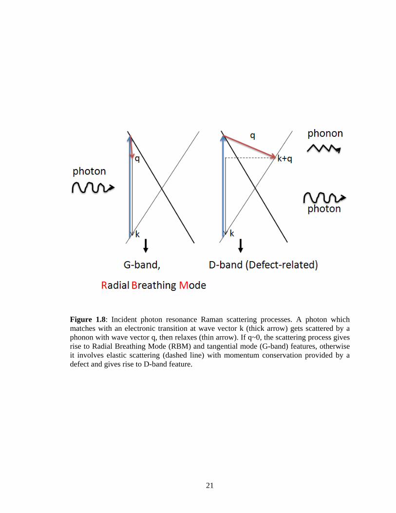
Figure 1.8: Incident photon resonance Raman scattering processes. A photon which matches with an electronic transition at wave vector k (thick arrow) gets scattered by a phonon with wave vector q, then relaxes (thin arrow). If q~0, the scattering process gives rise to Radial Breathing Mode (RBM) and tangential mode (G-band) features, otherwise it involves elastic scattering (dashed line) with momentum conservation provided by a defect and gives rise to D-band feature.
21

1 0 0 2 0 0 1 2 0 0 1 4 0 0 1 6 0 00
5 0 0
1 0 0 0
1 5 0 0In
tens
ity (a
.u.)
R a m a n sh ift (cm -1)
G bands-CNT
RBM
D-band
G band
m-CNT
2550 2600 2650 27001400 1500 1600 170
100
200
300
400
00
2D band
Inte
nsity
Raman shift (cm-1)
Figure 1.9: Raman spectrum with three main features: RBM, D-band, and G-band for a s-CNT (upper) and a m-CNT (lower) with broad and asymmetric Fano lineshape (thin line).
22

m-E11
s-E22
s-E11
Figure 1.10: Kataura plot in which each point corresponds to specific electronic transition energy Eii, nanotube diameter, and RBM frequency [15].
23

Catalyst islands patterned
CVD growth
CH4, H2, 900oC
Electrode deposition (Ti/Au)
Figure 1.11: Schematic of CNT synthesis, CNT-FET fabrication, and simultaneous Raman and transport measurements with polymer electrolyte top gating.
24

Figure 1.12: An AFM image of a single connection CNT-based FET.
25

CHAPTER 2
CHARGING TO ELUCIDATE ELECTRON-PHONON COUPLING
IN METALLIC CARBON NANOTUBES Significant part of this chapter has been published as “Fano Lineshape and Phonon
Softening in Single Isolated Metallic Carbon Nanotubes,” K. T. Nguyen, A. Gaur, and M.
Shim, Physical Review Letters 98, 145504 (2007).
2.1. Introduction
Electron-phonon interaction is critical for several important properties of CNTs,
including electrical transport [1, 2, 3, 4], superconductivity [5], and optical transitions
[6, 7]. The interaction between electrons and phonons is also important in Raman
scattering, affecting Raman intensity, frequency, and linewidth. In turn, inelastic
scattering can measure electron-phonon coupling [8, 9]. In this chapter, we will consider
the optical phonon-electron interaction as it gives rise to a striking difference between G
band feature of semiconducting and metallic SWCNTs.
Among various Raman features of SWCNTs, the broad and asymmetric Fano
lineshape has received much attention. Conflicting reports exist on the presence of the
broad downshifted G- peak in isolated versus bundled m-CNTs. Initially, this feature has
been attributed to phonon-plasmon coupling based on ensemble measurements [10].
Increasing linewidth and frequency downshift with decreasing average diameter have
appeared consistent with the assignment of G- peak as TO phonons (i.e. the
circumferential in-plane mode) and that the broad asymmetric lineshape is an intrinsic
characteristic [10]. In contrast, based on the argument that the available momentum of
26

incident photons for Raman measurements is too small for energy conservation in
phonon-plasmon coupling, coupling to a band of plasmons arising in bundles of
SWCNTs has been proposed to be the origin of the Fano lineshape rather than an intrinsic
process in single m-CNTs [11]. Comparisons of Raman measurements on individual
bundles and single metallic tubes have led to results where the broad, downshifted, and
asymmetric G- peak disappears upon de-bundling by mechanical manipulation [12] or by
low density CVD growth [13]. Narrow linewidth and frequency similar to s-CNTs should
then be the intrinsic attributes of m-CNTs. However, reference 11 predicts G- frequency
upshift with number of tubes in bundle, in contrast with other references which either
show a downshift [14] or tube diameter, not bundle size, dependence of G- frequency [10,
15] Therefore, the proposed phonon-plasmon/ band of plasmon coupling theory fails to
provide an explanation for experimental results.
The discrepancies between reports come from either measurement on bundles of
CNTs, where bundling effects and signal overlapping dominates, or the neglect of CNT-
environment interactions, for instance, charge transfer and defect formation. We utilize
effective polymer electrolyte gating with simultaneous Raman and electrical
measurements at individual SWCNT level, as depicted in figure 1.11, to provide new
insights, in particular, on how phonon modes involve with changing of the Fermi level.
16,17 Such measurements are especially important in elucidating what the inherent
phonon lineshape is and therefore what the mechanism that causes the broadening of G-
line is.
2.2. Fano Lineshape and Kohn Anomaly
27

Figure 2.1 shows D- and G-band regions of the Raman spectrum of a single m-
CNT at two different gate voltages, Vg. A single radial breathing mode (RBM) at 202.3
cm-1, which is resonant with 1.96eV excitation source, indicates that this is a metallic
tube. Narrow linewidth, FWHM = 6 cm-1, and the consistency of 1.3 nm diameter
obtained from AFM imaging with expected diameter of 1.2 nm based on the RBM
frequency shows that it is an isolated tube. There are large changes in the G-band upon
different Vg. The upper spectrum at Vg = 1.2V in figure 2.1 is fitted with two Lorentzians
for the G-band and one Lorentzian for the D-band. Both features of G-band have
frequencies similar to typical single s-CNT of comparable diameter [18, 19]. At Vg = –
0.2V, where the electrical conductance is minimum, which indicates that this potential
corresponds to the Fermi level being at the DP between the first pair of vHS, a broad
asymmetric Fano lineshape appears. The G-band region of the spectrum at DP is fitted to
three Lorentzians and one Fano line. The four features of the G-band are labeled P1
through P4. It is P1 that exhibits asymmetric Fano lineshape near DP but disappears at
high Vg. The curve fitting for all data presented here is carried out including the D-band
to ensure that changes in the D-band intensity are not mistaken for lineshape asymmetry.
In contrast to the high Vg all-Lorentzian spectrum, the asymmetric Fano component
arising near DP leads to a non-vanishing intensity well below the D-band region.
In addition to asymmetric lineshape, the spectrum at Vg = –0.2V also exhibits
broadened linewidths for all G-band modes. The two dominant peaks of the G-band at Vg
= 1.2V exhibit narrow linewidths (FWHM) of ~10 cm-1 whereas the corresponding two
peaks (P2 and P3) at Vg = –0.2V have FWHMs ~20 cm-1. The asymmetric component P1
also shows about a factor of 2 increase in linewidth near DP compared to Fermi level
28
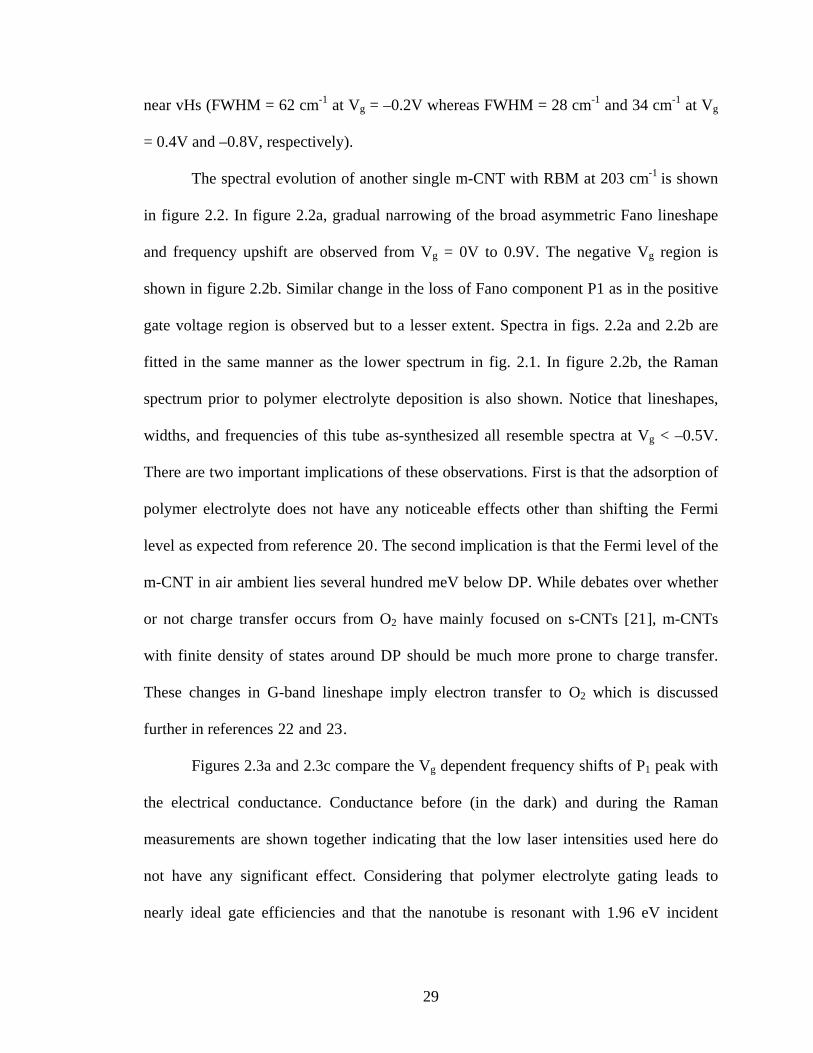
near vHs (FWHM = 62 cm-1 at Vg = –0.2V whereas FWHM = 28 cm-1 and 34 cm-1 at Vg
= 0.4V and –0.8V, respectively).
The spectral evolution of another single m-CNT with RBM at 203 cm-1 is shown
in figure 2.2. In figure 2.2a, gradual narrowing of the broad asymmetric Fano lineshape
and frequency upshift are observed from Vg = 0V to 0.9V. The negative Vg region is
shown in figure 2.2b. Similar change in the loss of Fano component P1 as in the positive
gate voltage region is observed but to a lesser extent. Spectra in figs. 2.2a and 2.2b are
fitted in the same manner as the lower spectrum in fig. 2.1. In figure 2.2b, the Raman
spectrum prior to polymer electrolyte deposition is also shown. Notice that lineshapes,
widths, and frequencies of this tube as-synthesized all resemble spectra at Vg < –0.5V.
There are two important implications of these observations. First is that the adsorption of
polymer electrolyte does not have any noticeable effects other than shifting the Fermi
level as expected from reference 20. The second implication is that the Fermi level of the
m-CNT in air ambient lies several hundred meV below DP. While debates over whether
or not charge transfer occurs from O2 have mainly focused on s-CNTs [21], m-CNTs
with finite density of states around DP should be much more prone to charge transfer.
These changes in G-band lineshape imply electron transfer to O2 which is discussed
further in references 22 and 23.
Figures 2.3a and 2.3c compare the Vg dependent frequency shifts of P1 peak with
the electrical conductance. Conductance before (in the dark) and during the Raman
measurements are shown together indicating that the low laser intensities used here do
not have any significant effect. Considering that polymer electrolyte gating leads to
nearly ideal gate efficiencies and that the nanotube is resonant with 1.96 eV incident
29

laser, the increase in the conductance at positive and negative Vg should correspond to
increasing electronic density of states as the Fermi level nears the first pair of vHs. The
conductance minimum at Vg ~ 0.2V then corresponds to the Fermi level at DP. The most
prominent effect on the Raman spectrum of a single isolated m-CNT as shown in figure
2.3a is the softening of P1 feature coincident with the conductance minimum. Concurrent
line broadening with softening as well as the correlation with conductance of coupling
parameter q, shown in figure 2.3b, suggests that electron-phonon coupling becomes
stronger near DP for P1.
In short, we have shown that Fano lineshape is inherent to single m-CNT and that
it is observable when the Fermi level is close to the band crossing point. The Fermi level
shift towards vHs changes the Fano lineshape to Lorentzian.
2.3. Physics of Raman Fano Component
Several theoretical studies have assigned the Fano component to the LO mode
that is softened by a Kohn anomaly (KA) at the Γ point in the phonon dispersion [24, 25,
26, 27]. The KA, or the sudden softening of phonon frequency resulting from an abrupt
change of the elecronic screening of atomic vibrations, happens in the LO phonon branch
as LO phonon distorts the lattice such that a dynamic bandgap is induced in the electronic
structure as demonstrated in figure 2.4 for an armchair CNT [24] The electronic band
structure of CNTs is obtained from band structure of graphene which consists of cones
intersecting at 6 corners, K point or DP, of the 2D Brillouin zone, by zone folding
argument, i.e. by the intersection of the cones with those planes that are allowed by the
conditions imposed by the wrapping procedure [28] Since the reciprocal lattice can be
obtained by turning the real lattice 900 for graphene, the LO mode makes the tip of the
30
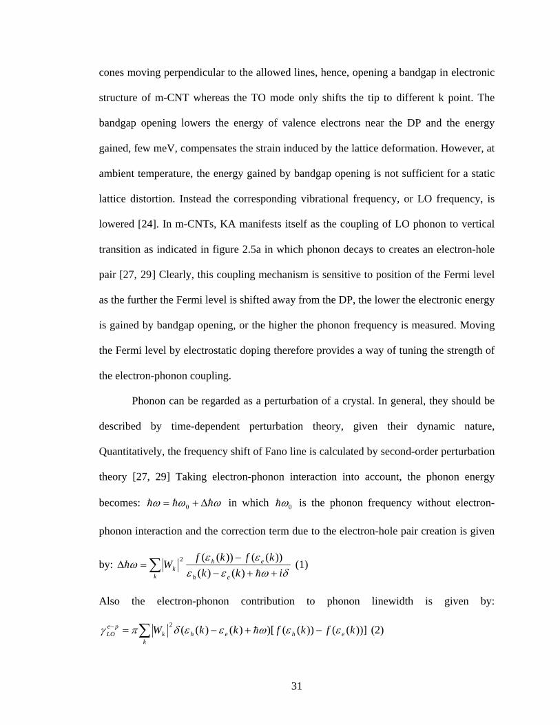
cones moving perpendicular to the allowed lines, hence, opening a bandgap in electronic
structure of m-CNT whereas the TO mode only shifts the tip to different k point. The
bandgap opening lowers the energy of valence electrons near the DP and the energy
gained, few meV, compensates the strain induced by the lattice deformation. However, at
ambient temperature, the energy gained by bandgap opening is not sufficient for a static
lattice distortion. Instead the corresponding vibrational frequency, or LO frequency, is
lowered [24]. In m-CNTs, KA manifests itself as the coupling of LO phonon to vertical
transition as indicated in figure 2.5a in which phonon decays to creates an electron-hole
pair [27, 29] Clearly, this coupling mechanism is sensitive to position of the Fermi level
as the further the Fermi level is shifted away from the DP, the lower the electronic energy
is gained by bandgap opening, or the higher the phonon frequency is measured. Moving
the Fermi level by electrostatic doping therefore provides a way of tuning the strength of
the electron-phonon coupling.
Phonon can be regarded as a perturbation of a crystal. In general, they should be
described by time-dependent perturbation theory, given their dynamic nature,
Quantitatively, the frequency shift of Fano line is calculated by second-order perturbation
theory [27, 29] Taking electron-phonon interaction into account, the phonon energy
becomes: ωωω hhh Δ+= 0 in which 0ωh is the phonon frequency without electron-
phonon interaction and the correction term due to the electron-hole pair creation is given
by: ∑ ++−−
=Δk eh
ehk ikk
kfkfW
δωεεεε
ωh
h)()(
))(())((2 (1)
Also the electron-phonon contribution to phonon linewidth is given by:
∑ −+−=−
kehehk
peLO kfkfkkW ))](())(()[)()((2 εεωεεδπγ h (2)
31

where is the strength of the electron-phonon interaction in creating electron-hole pair
at momentum k,
kW
)(εf is the Fermi-Dirac distribution with a variable Fermi level EF,
)(keε and )(khε are the electron and hole energy, respectively, δ is the decay width, and
)(εδ is the Dirac distribution. We need to sum over all possible intermediate electron-
hole pair states in equation (1) and (2), which can have energy ε = )()( kk eh εε − much
larger than phonon energy ωh , and at T=0 K:
2/12
0022
202
0 )2
22ln
32()(
−Γ
−+><+=
k
EED
Mda
E FFFF
β
ωωβπ
ωωhh
Electron-phonon contribution to LO linewidth at temperature T:
]1
11
1[79)( /)2/(/)2/(
1
00 +−
+= +−
−−
TkETkEFpe
LO BFBF eednmcmE ωωγ
hh
in which is the lattice parameter, M is the atomic mass of carbon, ω0a 0 is the bare
frequency, the graphene electron-phonon coupling = 45.6 (eV/AFD >< Γ2 0)2, =0.1
−
k0
2aπ ,
and π
β2
)1.14( 0aeV= .
At T= 0 K, the two singularities appear at which the electron-phonon interaction
is strongest because the resonance of phonon energy and the real electronic interband
excitation. This divergence is responsible for the abrupt change in phonon frequency, or
Kohn anomaly. However, we do not see these singularities in our experiment since
energy level broadens at higher temperature [25, 27]. Instead, we expect to see LO
phonon softening and broadening when Fermi level is close to the DP as demonstrated in
figure 2.5b whereas TO frequency should stay constant since TO mode is not supposed to
32

exhibit KA [25, 27]. Our result on LO phonon qualitatively agrees with this prediction as
shown in figure 2.6 and 2.7. The only fitting parameter is the gate coupling efficiency,
taken as 0.4. However, the degree of LO phonon spectrum softening and broadening is
smaller than the calculated for m-CNT with moderate degree of defect (figure 2.6). For
another m-CNT, which does not exhibit significant amount of defect, we see a good fit
between theoretical calculation and experimental results (figure 2.7). We also see TO
phonon softening and there is no crossing between LO and TO modes as predicted. These
discrepancies will be discussed in chapter 3 in light of defect dependence.
In m-CNTs, the strong electron-phonon coupling gives rise to Kohn anomaly in
LO mode which is evidenced by LO phonon softening and broadening when the Fermi
level is close to the DP. Kohn anomaly softens LO frequency much stronger than
curvature effect on TO mode and thus, in m-CNT, the lower frequency peak, G-, is
assigned to LO mode, and the higher one, G+, to TO mode [22-25] This assignment is
opposite to s-CNTs in which Kohn anomaly is not supposed to occur as their band gap is
larger than phonon energy and there is no resonance of phonon energy and interband
electronic excitation. This will be discussed further in chapter 4.
The gate dependence of RBM mode is shown in figure 2.7. When the Fermi level
is close to the DP, not only the LO mode softens but also RBM mode. However RBM
mode softens only 2 cm-1 and RBM linewidth stays almost constant over the wide range
of gate voltage, in contrast to the broadening of LO phonon mode. The behaviors of
RBM mode can be understood by considering that, like LO phonon, RBM phonon can
excite vertical electron-hole pairs, thus, renormalizing phonon energy [29, 30].
Nevertheless, RBM phonon energy is 25 meV, a small fraction of LO phonon energy
33

(190 meV), the electron-hole pair excitations for RBM occur much closer to the DP. At
this energy scale the curvature-induced bandgap [31] becomes significant. For this (14,2)
m-CNT, the bandgap is 42 meV according to references 30 and 32, which exceeds RBM
phonon energy, hence, there is no real vertical transition and linewidth does not broaden.
2.4. References 1. C. L. Kane, E. J. Mele, R. S. Lee, J. E. Fischer, P. Petit, H. Dai, A. Thess, R. E.
Smalley, A. R. M. Verschueren, S. J. Tans, C. Dekker, Europhys. Lett. 41, 683–688
(1998).
2. J. Y. Park, S. Rosenblatt, Y. Yaish, V. Sazonova, H. Ustunel, S. Braig, T. A. Arias,
P.W. Brouwer, P. L. McEuen, Nano Lett. 4, 517–520 (2004).
3. Z. Yao, C. L. Kane, C. Dekker, Phys. Rev. Lett. 84, 2941–2944 (2000).
4. A. Javey, J. Guo, M. Paulsson, Q. Wang, D. Mann, M. Lundstrom, H. J. Dai, Phys.
Rev. Lett. 92, 106804 (2004).
5. Z. K. Tang, L. Zhang, N. Wang, X. X. Zhang, G. H. Wen, G. D. Li, J. N. Wang, C. T.
Chan, P. Sheng, Science 292, 2462 (2001).
6. S. B. Cronin, Y. Yin, A. Walsh, R. B. Capaz, A. Stolyarov, P. Tangney, M. L.Cohen,
S. G. Louie, A. K. Swan, M. S. Unlü, B. B. Goldberg, M. Tinkham, Phys. Rev. Lett.
96, 127403 (2006).
7. V. Perebeinos, J. Tersoff, P. Avouris, Phys. Rev. Lett. 94, 027402 (2005).
8. S. Piscanec, M. Lazzeri, M. Mauri, A. C. Ferrari, J. Robertson, Phys. Rev. Lett. 93,
185503 (2004).
9. M. Lazzeri, S. Piscanec, F. Mauri, A. C. Ferrari, J. Robertson, Phys. Rev. B 73,
155426 (2006).
34

10. S. D. M. Brown, A. Jorio, P. Corio, M. S. Dresselhaus, G. Dresselhaus, R. Saito, K.
Kneipp, Phys. Rev. B 63, 155414 (2001).
11. K. Kempa, Phys. Rev. B 66, 195406 (2002).
12. C. Jiang, K. Kempa, J. Zhao, U. Schlecht, U. Kolb, T. Basché, M. Burghard, A.
Mews, Phys. Rev. B 66, 161404 (2002).
13. M. Paillet, P. Poncharal, A. Zahab, J. L. Sauvajol, J. C. Meyer and S. Roth, Phys.
Rev. Lett. 94, 237401 (2005).
14. M. Pailet, P. Poncharal, A. Zahab, J. L. Sauvajol, J. C. Meyer, S. Roth, Appl. Phys.
Lett. 94, 237401 (2005).
15. M. Oron-Carl, F. Hennrich, M. M. Kappes, H. v. Lohneysen, R. Krupke, Nano Lett.
5, 1761 (2005).
16. S. B. Cronin, R. Barnett, M. Tinkham, S. G. Chou, O. Rabin, M. S. Dresselhaus, A.
K. Swan, M. S. Ünlü, and B. B. Goldberg, Appl. Phys. Lett. 84, 2052 (2004).
17. Z. Wang, H. Pedrosa, T. Krauss, L. Rottberg, Phys. Rev. Lett. 96, 047403(2006).
18. A. Jorio, M. A. Pimenta, A. G. Souza Filho, Ge. G. Samsonidze, A. K. Swan, M. S.
Ünlü, B. B. Goldberg, R. Saito, G. Dresselhaus, and M. S. Dresselhaus, Phys. Rev.
Lett. 90, 107403 (2003).
19. M. Paillet, T. Michel, J. C. Meyer, V. N. Popov, L. Henrard, S. Roth, J. –L. Sauvajol,
Phys. Rev. Lett. 96, 257401 (2006).
20. M. Shim, T. Ozel, A. Gaur, and C. Wang, J. Am. Chem. Soc. 128, 7522 (2006).
21. M. Shim, J. H. Back, T. Ozel, and K. W. Kwon, Phys. Rev. B 71, 205411 (2005); S.
Heinze, J. Tersoff, R. Martel, V. Derycke, J. Appenzeller, Ph. Avouris, Phys. Rev.
35

Lett. 89, 106801 (2002) ; P. G. Collins, K. Bradley, M. Ishigami, A. Zettl, Science
287, 1801 (2000).
22. A. Gaur, M. Shim, Phys. Rev. B 78, 125422 (2008).
23. M. Shim, A. Gaur, K. T. Nguyen, D. Abdula, and T. Ozel, J. Phys. Chem. C. 112,
13017 (2008).
24. O. Dubay, G. Kresse, and H. Kuzmany, Phys. Rev. Lett. 88, 235506 (2002).
25. M. Lazzeri, S. Piscanec, F. Mauri, A. C. Ferrari, J. Robertson, Phys. Rev. B 73,
155426 (2006).
26. V. N. Popov and P. Lambin, Phys. Rev. B 73, 085407 (2006).
27. N. Caudal, A. M. Saitta, M. Lazzeri, F. Mauri, Phys. Rev. B 75, 115423 (2007).
28. J. W. Mintmire, C. T. White, Phys. Rev. Lett. 81, 2506 (1998).
29. J. C. Tsang, M. Freitag, V. Perebeinos, J.Liu, Ph. Avouris, Nature Nanotech. 2, 725
(2007).
30. H. Farhat, K. Sasaki, M. Kalbac, M. Hofmann, R. Saito, M. S. Dresselhaus, J. Kong,
Phys. Rev. Lett. 102, 126804 (2009).
31. C. L. Kane, E. J. Mele, Phys. Rev. Lett. 78, 1932 (1997).
32. K. Sasaki, R. Saito, G. Dresselhaus, M. S. Dresselhaus, H. Farhat, J. Kong, Phys. Rev.
B 78, 235405 (2008).
36

2.5. Figures
igure 2.1: Raman spectra of a single isolated m-CNT at the indicated gate voltage Vg (in
1200 1300 1400 1500 1600 1700
P3P4
P2P1
1558.7(10.0)
1592.7(11.1)
Inte
nsity
(arb
. uni
ts)
Raman Shift (cm-1)
Vg = -0.2V
Vg = 1.2V
Fbold) with corresponding position of Fermi level EF. Gray lines are the data and the bold black lines are the curve fits as described in the text. Thin lines are components of the curve fit with P1 – P4 designated for lower spectrum. Numbers in the upper spectrum correspond to peak position (width) in cm-1. Spectra are offset for clarity.
37

Figure 2.2: Raman spectra of a m-CNT at positive (a) and negative (b) gate voltages Vg swept from –1 to +1 V at 0.1 V step. Spectra at 0.2V intervals and at 0V are shown and offset for clarity. Top spectrum in (b) and RBM in inset of (a) correspond to the same tube prior to polymer electrolyte deposition without applied Vg. Peak position (width) for RBM is indicated.
38

(a)
(b)
(c)
Figure 2.3: Vg dependence of frequency shifts (a) and Fano line coupling parameter q for P1 (b) compared with conductance (c) of the same tube as in figure 2.2. Open squares (line) are conductance during (before) Raman measurements.
39

a) No displacement b) TO mode
c) LO mode
Figure 2.4: (a) Electronic band structure of graphene in the vicinity of K point of the Brillouin zone (hexagon). The thick lines indicate the band structure of an armchair nanotube obtained by intersecting the gray plane with the two cones. (b) For TO mode, the crossing point shifts along the KΓ line, thus the band structure of the nanotube does not change. (c) For LO mode, the crossing point shifts perpendicular to the KΓ line and opens a gap (double head arrow) [24].
40

(a) ωh
(b) Figure 2.5: (a) An intermediate electron-hole pair (presented by a loop) state that contributes to the energy shift of phonon modes (presented by zigzag lines) is depicted. (b) The predicted dependence of LO and TO phonon frequency on position of the Fermi level for (9, 9) m-CNT [27, 29].
41

-0.3 -0.2 -0.1 0.0 0.1 0.2 0.320
40
60
80
Fano
line
wid
th (c
m-1)
EF (eV)
-0.3 -0.2 -0.1 0.0 0.1 0.2 0.31520
1530
1540
1550
1560
Fano
freq
uenc
y (c
m-1)
EF (eV)
Figure 2.6: Linewidth (upper) and frequency (lower) of Fano component as a function of Fermi level EF of the same m-CNT shown in figure 2.3. The solid line in the upper panel and the dash line in the lower are the calculated linewidths (T=300K) and frequencies (T=0K) from reference 27. Our experimental results on LO mode qualitatively agrees with theoretical prediction. However, the degree of LO phonon softening and broadening is smaller than the calculated for this m-CNT which exhibits moderate degree of defect.
42

-0.3 -0.2 -0.1 0.0 0.1 0.2 0.3
20
30
40
Fano
line
wid
th (c
m-1)
EF (eV)
-0.3 -0.2 -0.1 0.0 0.1 0.2 0.31568
1572
1576
1580
Fano
freq
uenc
y (c
m-1)
EF (eV)
Figure 2.7: Linewidth (upper) and frequency (lower) of Fano component as a function of Fermi level EF of another m-CNT with RBM frequency at 104 cm-1 and nearly free of defect. The solid line in the upper panel and the dash line in the lower are the calculated linewidths (T=300K) and frequencies (T=0K) from reference 27. There is a good fit between experimental data and theoretical calculation.
43

-1.0 -0.5 0.0 0.5 1.0202.5
203.0
203.5
204.0
204.5
RBM
Fre
quen
cy (c
m-1)
Gate Voltage (V)
-1.0 -0.5 0.0 0.5 1.04.0
4.5
5.0
5.5
6.0
6.5
7.0
7.5
8.0
RBM
Lin
ewid
th (c
m-1)
Gate Voltage (V)
Figure 2.8: Gate dependence of RBM frequency (upper) and linewidth (lower). Straight line guides the eyes. RBM mode softens only 2 cm-1 and its linewidth stays almost constant. RBM phonon can excite vertical electron-hole pairs, thus, renormalizing phonon energy but linewidth does not broaden since there is no real vertical electronic excitation.
44

CHAPTER 3
DEFECTS IN METALLIC CARBON NANOTUBES Significant part of this chapter has been published as “Role of Covalent Defects on
Phonon Softening in Metallic Carbon Nanotubes”, K. T. Nguyen and M. Shim, Journal
of American Chemical Society 131, 7103 (2009). The subsection 3.1 has been published
as a part of “Raman Spectral Evolution in Individual Metallic Single-Walled Carbon
Nanotubes upon Covalent Bond Formation”, D. Abdula, K. T. Nguyen, and M.
Shim, Journal of Physical Chemistry C 111, 17755 (2007), and “Spectral Diversity in
Raman G-band Modes of Metallic Carbon Nanotubes within a Single Chirality”, M.
Shim, A. Gaur, K. T. Nguyen, D. Abdula, and T. Ozel, J. Phys. Chem. C. 112, 13017
(2008).
3.1. Charging, Defect, and Defect Characterization
3.1.1. Doping Dependence of Defect-Induced D-band
In chapter 2, we have discussed about the effect of the Fermi level shift induced
by electrostatic doping: the onset of coupling between LO phonon to electronic
continuum around DP, or Kohn anomaly. This special coupling leads to the softening of
LO mode in Raman G-band when the Fermi level is close to the DP, and the softening is
symmetric for electron and hole doping [1, 2, 3, 4]. Another effect is the change of
equilibrium lattice parameter that can be seen from charging dependence of Raman D-
band phonon energy as shown in figure 3.1 for the same m-CNT that has Raman G-band
shown in figure 2.1. When a positive gate voltage is applied, electrons are injected into
the antibonding states, resulting in an expansion of C-C bonds [5], and a consequent
45

decreasing of D-band phonon frequency. In contrast, when holes are injected into
bonding states at negative voltages, bond contraction occurs, and D-band frequency
increases. In principle, charging dependence of D band phonon frequency is influenced
by both electron-phonon interaction [6] and conventional lattice expansion/contraction
upon doping. However, impact of the former on D band phonon is one order of
magnitude weaker than on G band phonon as reported by several research groups [7, 8].
Therefore, the latter plays dominant role and being partially compensated by the former
which results in the doping independence of D band frequency over a range of gate
voltage around –0.5V as shown in figure 3.1. The dependence of D-band frequency on
doping is different from G-band feature, and can differentiate electron or hole doping.
3.1.2. Degree of Defect Characterization
Although the doping dependence of D band and G band phonon frequencies are
different, the ratio of integrated intensities of D and G bands in the Raman spectra has
been often used as an indication of covalent functionalization of SWCNTs as well as in
identifying amorphous carbon contamination [9]. The rationale for using D to G intensity
ratio as a measure of degree of functionalization is from the fact that the D-band arises
from disorder scattering. Simultaneous Raman and transport measurement can trace not
only G-band but also D-band spectral evolution upon charging, as seen from fig. 2.2a and
2.2b. The enhancement of D-band intensity and the broadening of G-band appear
concurrently when the Fermi level is close to the DP. In light of Fermi level shift
dependence of G-band lineshapes and D-band intensity, using D- to G-band integrated
intensity ratio, ID/IG, as an indication of the degree of defect in m-CNTs needs to be
considered carefully.
46
Figure 3.2a shows the gate dependence of ID/IG where we have not considered the
asymmetry of the lowest frequency G-band peak of the same tube. The inset shows the
corresponding integrated area under each band for the spectrum collected at Vg = 0V.
There appears to be a large gate voltage dependence. If ID/IG without considering the
asymmetry of Fano line is used as an assessment of defect introduction, the increase in
ID/IG arising from the Fermi level shift can be easily misinterpreted as defect formation as
larger degree of defects should lead to a more pronounced D-band. Because the lineshape
of the lowest frequency peak of the G-band features converts from Lorentzian to Fano
lineshape as the Fermi level shifts from either one of the nearest vHs to the band crossing
point, the integrated intensity of the G-band should include the lineshape asymmetry.
Figure 3.2b shows ID/IG of the same metallic tube when the Fano lineshape is
included as shown in the inset. In this case, ID/IG remains independent of the Fermi level
shift as it should be since no more physical disorder is introduced. These results indicate
that we can utilize ID/IG as a qualitative measure of defect formation of metallic tubes
only if we include the Fano line area which extends below the D-band frequency range,
and this is applied in the following section.
3.2. Covalent Defect Introduction to Metallic Nanotubes
3.2.1. Motivation
In light of the fact that most as-synthesized m-CNTs exhibit measurable D-band
intensities, an indication of sensitivity of metallic tubes with adsorbed molecules [8, 9,
13], the influence of physical disorder on Raman spectra of m-CNTs needs to be
investigated. Figures 3.3a and 3.3b show the LO frequency increasing and LO linewidth
47

decreasing, respectively, with defect density across several m-CNTs. These behaviors
appear to be similar to charging induced changes as discussed in chapter 2, and charging
effects and influences of defects need to be sorted out. The relation between the degree of
charging and the degree of disorder is also critical especially in characterizing chemical
functionalization and doping processes that involve charge transfer. Furthermore, as-
synthesized m-CNTs that are exposed to air ambient exhibit a wide distribution of
phonon frequencies and linewidths even within a single chirality [10] that makes it
difficult to determine the intrinsic parameters, and to compare to theoretical predictions.
While much of the distribution has been shown to arise from the variations in the Fermi
level position (charging) with one key cause being exposure to ambient oxygen [2, 7, 11],
there is no obvious relation between the degree of charging and the degree of disorder,
both of which appear upon oxygen exposure. Therefore, interpretation of experimental
results remains an issue.
Another complication is in whether or not the Raman TO mode softens as
mentioned in chapter 2. There have been apparent discrepancies in experimentally
observed behavior of the TO mode – i.e. some reports show TO mode softening [2, 3],
some show that it doesn’t [1, 5], yet others show both behaviors [12]. While progress has
been made in understanding charging dependent Raman spectral changes, very little
attention has been given on how disorder complicates these spectral changes. Beyond the
increasing D-band intensity and the appearance of the so-called D’ shoulder at the high
frequency side of the G-band, only limited information about how covalent reactions alter
Raman spectra in CNTs is available.
48

Simultaneous Raman and electrochemical gating studies on single isolated m-
CNTs at different stages of covalent defect introduction (i.e. following the same m-CNT
while increasing degree of disorder) may separate out the role of disorder from charging
effects on the Raman active modes of SWCNTs. Here, we introduce increasing degree of
covalent defects via reaction with increasing concentration of 4-bromobenzene
diazonium tetrafluoroborate (4-BBDT) and examine the charging dependent G-band
Raman spectral evolution of individual m-CNTs after each reaction step with 4-BBDT.
Functionalization was carried out with 4-BBDT of desired concentrations in water for 15
minutes. Polymer electrolyte medium, which is described in chapter 1, was removed by
rinsing thoroughly with methanol before each reaction and then applied again for
subsequent studies. This choice of the chemical reagent for introducing defects may also
lead to further insights in developing simple scalable electronically selective chemistry
for SWCNTs since 4-BBDT has shown some selectivity towards m-CNTs [13, 14, 15]
Adding covalent chemical groups to the sidewalls influences not only the electronic
properties but also the phonon characteristics [16] Therefore, chemical functionalization
may facilitate pathways to electronic and phonon band structure engineering in addition
to selectively sorting out metallic and semiconducting SWCNTs for nanoelectronics and
sensor applications.
Reaction with 4-BBDT is presumably initiated by charge transfer [10a] and may
shift the Fermi level of m-CNTs. Such Fermi level shifts, as we show here, can
complicate comparisons between Raman features before and after the reaction because
the Raman modes are both charge and defect dependent. By measuring Raman spectra at
different electrostatic doping levels, we can directly examine how Raman spectra at the
49

same Fermi level position, especially near the charge neutrality point, evolve with
increasing covalent defects. Changes in charging dependent softening of both LO and TO
modes of metallic SWCNTs upon covalent defect introduction are investigated.
Implications on comparing expected and experimentally observed G-band phonon
softening and on Raman characterization of covalent functionalization are discussed.
3.2.2. Influences of Defects on Electrical Properties
In fig. 3.4, we show the D- and the G-band regions of the Raman spectra of a m-
CNT at each step of the reaction with 4-BBDT. The inset is the radial breathing mode
(RBM) seen at 167 cm-1 before the reaction. The Raman spectra are collected with
applied electrochemical gate potential to ensure that the Fermi level lies near the DP
where the SWCNT is charge neutral. Each spectrum is fitted with one Lorentzian for the
D-band around 1320 cm-1 and one Fano line and three Lorentzians for the G-band.
Following references 2 and 11, we refer to the Fano peak labeled P1 as the LO mode and
Loretzian peak labeled P3 as the TO mode.
Figure 3.5a shows the enhancement of D to G-band integrated intensity ratio,
ID/IG, of a m-CNT due to increasing reaction concentration of 4-BBDT, at 0, 10 and 50
μM 4-BBDT, confirming introduction of covalent defects. As a consequence of
increasing defect scattering, there is a large overall decrease in the conductance from 1.6
μS to 1.4 x 10⁻² μS as seen in figure 3.5a. Figure 3.5b shows how the electrical
conductance (normalized to the maximum conductance for comparison), changes upon
reaction with 4-BBDT. The enhancement of gate dependence can actually be observed
here, i.e. increasing on/off current ratio from ~2 before reaction to ~300 after reacting
with 50 μM 4-BBDT, resulting in semiconductor-like behavior.
50

3.2.3. Influences of Defects on Phonon Properties
Adding covalent chemical groups to the CNT sidewalls influences not only the
electronic properties but also the phonon characteristics. The gate voltage dependence of
LO phonon frequency, ωLO, and linewidth, ΓLO, before any reaction and after reaction
with 10 and 50 μM 4-BBDT are shown in figures 3.6a and 3.6b. The qualitative
dependence to charging is the same in all three cases. That is, the expected phonon
softening and broadening of the LO mode occurs near the band crossing point (DP) at all
stages of the covalent reaction. The difference lies in the degree of softening and
broadening. The decreasing degree of phonon softening and broadening upon increasing
covalent disorders is shown for three different m-CNTs in figure 3.7. The main panel is
the change in the minimum ωLO (ΔωLO, min). The inset is the change in the maximum ΓLO
(ΔΓLO, max). Covalent chemical functionalization disrupts the π bonding system by
replacing haft-filled pz orbital by an sp3 bonding orbital at some sites. As a consequence,
adding covalent disorders can remove electronic states near the band crossing point and
eventually open a band gap in m-CNTs [17] Increasing defect density from covalent
reaction with 4-BBDT then is likely to be reducing the density of states (DOS) near DP
which in turn reduces free carrier density. The increasing gate dependence of
conductance leading to semiconductor-like behavior after reaction with 50 μM 4-BBDT
shown in figure 3.5b supports the idea of reduction in DOS near DP. Carrier scattering
from defects would decrease the overall conductivity but does not necessarily lead to
enhanced gate dependence. The change in the electronic structure especially about DP
then reduces the degree of electron-phonon coupling induced effects (i.e. alleviating the
Kohn anomaly induced phonon softening and line broadening) leading to the
51

observations in figure 3.6 where the degree of LO phonon softening and broadening
decreases with increasing covalent defect density.
While the LO mode exhibits behavior consistent with the gradual removal of
Kohn anomaly induced phonon softening, increasing defect density leads to enhanced
softening of the TO mode. Figure 3.8a shows how the gate dependence of ωTO changes
with covalent functionalization for the same m-CNT shown in figure 3.4. Data for
another m-CNT, which exhibits a larger change, is presented in figure 3.8b. The SWCNT
in figure 3.8b initially exhibited no observable D-band intensity and the low degree of
initial disorder in this SWCNT may be the main reason for the larger change.
Nevertheless, as figure 3.9 indicates, all three m-CNTs examined here show the same
trend of TO mode softening near DP with increasing defect density. Another effect of
covalent functionalization which introduces local sp3 defects, disrupting the sp2 system is
the increasing of average bond length, which should then, in principle, lead to softening
of all in-plane modes (i.e. both TO and LO modes). This defect induced softening is
observed in TO mode which is expected to be independent of Kohn anomaly effects near
DP. LO mode, on the other hand, exhibits stiffening with increasing defect density
because the reduction in electron-phonon coupling induced effects is dominating the
spectral changes.
Besides the softening near the band crossing point, another notable change to TO
mode upon covalent functionalization is that it stiffens much more readily upon charging.
That is, a much larger change in ωTO can be seen with the same applied gate voltage
when the SWCNT is more defective. Because of the electron-phonon coupling matrix
element for the TO mode being zero, initial theoretical studies have led to the expectation
52

that TO mode does not soften like the LO mode and therefore ωTO should be independent
of charging [1, 5] However, both charge dependent and independent ωTO have been
observed experimentally [2, 3, 9] Most recently, these apparently contradicting results
have been suggested to arise from chirality-dependent behavior [9]. Achiral m-CNTs are
expected to exhibit only LO mode softening. Chiral m-CNTs can exhibit softening of
both LO and TO modes because the TO mode is not exactly along the circumferential
direction. While such chirality dependent behavior can be expected, our results in figures.
3.8 and 3.9 indicate that the degree of disorder may sometimes have a larger influence on
the observed softening of the TO mode.
In conclusion, we have shown that softening of both LO and TO modes of m-
CNTs is sensitive not only to Fermi level position but also to the degree of disorder. With
increasing defect density, LO mode stiffens whereas the TO mode softens. These
observations imply that reported experimental LO mode frequencies may be higher than
the intrinsic frequencies due to the presence of physical disorder, which is observed via
measurable D-band intensities in majority of individual m-CNTs. The degree of TO
mode softening is also dependent on degree of defects. Covalent disorders complicate the
doping dependence of both LO and TO phonon modes and can cause the crossing of LO
and TO frequency to be not observable. Furthermore, monitoring chemical reactions that
form covalent bonds via Raman spectroscopy should take into account both the Fermi
energy position and disorder dependent changes in the Raman features. We have also
shown the monotonic dependence of defect induced D-band frequency on the Fermi level
position, that is different from Raman G-band and can differentiate electron and hole
injection in SWCNTs.
53
3.3. References
1. N. Caudal, A. M. Saitta, M. Lazzeri, F. Mauri, Phys. Rev. B 75, 115423 (2007).
2. K. T. Nguyen, A. Gaur, M. Shim, Phys. Rev. Lett. 98, 145504 (2007).
3. H. Frahat, H. Son, G. G. Samsonidze, S. Reich, M. S. Dresselhaus, J. Kong, Phys.
Rev. Lett. 99, 145506 (2007).
4. J. C. Tsang, M. Freitag, V. Perebeinos, J.Liu, Ph. Avouris, Nature Nanotech. 2, 725
(2007).
5. M. S. Dresselhaus, G. Dresselhaus, Adv. Phys. 51, 1-186 (2002).
6. S. Piscanec, M. Lazzeri, M. Mauri, A. C. Ferrari, J. Robertson, Phys. Rev. Lett. 93,
185503 (2004)
7. P. Rafailov, J. Maultzsch, C. Thomsen, U. D.-Weglikowska, S. Roth, Nano Lett. 9,
3343 (2009).
8. J. Yan, Y. Zhang, P. Kim, A. Pinczuk, Phys. Rev. Lett. 98, 166802 (2007).
9. (a) J. L. Bahr, J. P. Yang, D. V. Kosynkin, M. J. Bronikowski, R. E. Smalley, J. M.
Tour, J. Am. Chem. Soc. 123, 6536 (2001). (b) M. Holzinger, J. Abraha, P. Whelan,
R. Graupner, L. Ley, F. Hennrich, M. Kappes, A. Hirsch, J. Am. Chem. Soc. 125,
8566 (2003). (c) J. M. Simmons, B. M. Nichols, S. E. Baker, M. S.Marcus, O. M.
Castellini, C. S. Lee, R. J. Hamers, M. A. Eriksson, Journal of Physical Chemistry B
110, 7113 (2006).
10. M. Shim, A. Gaur, K. T. Nguyen, D. Daner, T. Ozel, J. Phys. Chem. C 112, 13017
(2008).
11. A. Gaur, M. Shim, Phys. Rev. B 78, 125422 (2008).
54

12. K. Sasaki, R. Saito, G. Dresselhaus, M. S. Dresselhaus, H. Farhat, J. Kong, Phys.
Rev. B 77, 245441 (2008).
13. (a) M. S. Strano, C. A. Dyke, M. L. Usrey, P. W. Barone, M. J. Allen, H. Shan, C.
Kittrell, R. H. Hauge, J. M. Tour, R. E. Smalley, Science 301, 1519 (2003); (b) C.
Wang, Q. Cao, T. Ozel, A. Gaur, J. A. Rogers, M. Shim, J. Am. Chem. Soc. 127,
11460 (2005).
14. (a) K. Balasubramanian, R. Sordan, M. Burghard, K. Kern, Nano Lett. 4, 827 (2004).
(b) L. An, Q. Fu, C. Lu, J. Liu, J. Am. Chem. Soc. 126, 10520 (2004).
15. D. Abdula, K. T. Nguyen, M. Shim, J. Phys. Chem. C 111, 17755 (2007).
16. C. Fantini, M. A. Pimenta, M. S. Strano, J. Phys. Chem. C 112, 13150 (2008).
17. Y, -S, Lee, M. B. Nardelli, N. Marzari, Phys. Rev. Lett. 95, 076804 (2005).
55

3.4. Figures
Figure 3.1: Gate voltage dependence of D-band frequency, which can differentiate hole and electron injections.
56

-1.0 -0.5 0.0 0.5 1.00.1
0.2
0.3
1300 1400 1500 1600 17000
100
200
300
400V
g = 0V
GD
Inte
nsity
(arb
. uni
ts)
Raman Shift (cm-1)
Inte
grat
ed In
tens
ity R
atio
Gate Voltage (V)
(A) (B)
-1.0 -0.5 0.0 0.5 1.00.1
0.2
0.3
1200 1300 1400 1500 1600 17000
100
200
300
400Vg = 0V
GD
Inte
nsity
(arb
. uni
ts)
Raman Shift (cm-1)
Inte
grat
ed In
tens
ity R
atio
Gate Voltage (V)
Figure 3.2: Gate voltage dependence of D- to G-band integrated intensity ratios whenthe Fano lineshape is not considered (A) and when the asymmetric Fano lineshape istaken into account (B). Lines are guides to the eye. Insets show the correspondingintegrated areas for the D (red) and G (blue) regions for the Raman spectrum collectedat Vg = 0V.
57

(a)
(b)
Figure 3.3: Linewidth narrowing (a) and frequency upshift (b) with increasing defect across several m-CNTs, similar to doping induced changes.
58

1350 1500 16500
200
400
600
P4P3
P2P1
50μM
10μM
0μM
Inte
nsity
(a.u
.)
Raman shift (cm-1)
150 175 2000
150Intensity (a.u.)
Raman shift (cm -1)
Figure 3.4: Upper: Schematic of reaction between m-CNT and 4-BBDT; lower: Raman D- and G-band modes along with corresponding curve fits at different stages of covalent defect introduction without polymer electrolyte and without applied Vg. Curve fitting as described in the text is shown along with the spectra. Inset is the radial breathing mode region before reaction.
59

(a)
0 10 20 30 40 50
0.1
0.2
0.3
0.4
4-BBDT Concentration (μM)
I D/I G
0.01
0.1
1
Maxim
um conductance (μS
)
(b)
-1 0 1
1E-3
0.01
0.1
1
50μM
10μM
0μM
Nor
mal
ized
con
duct
ance
Vg (V)
Figure 3.5: Integrated D/G intensity ratio (ID/IG) and maximum conductance vs. reaction concentration of 4-BBDT (a). Gate voltage (Vg) dependent electrical conductance of one m-CNT after reaction with indicated concentration of 4-BBDT. The conductance is normalized to the maximum conductance for comparison. “0 μM” refers to spectrum as fabricated before the reaction (b).
60

-1 0 1
20
30
40
50
60
Γ LO (c
m-1)
Vg (V)-1 0 1
1550
1555
1560
Figure 3.6: Gate dependence of G-band LO frequency (a) and linewidth (b) of the samem-CNT shown in figure 3.4 after reaction with 0 (squares), 10 (circles), and 50μM(triangles) 4-BBDT concentrations.
(b)
ωLO
-1
Vg (V)
)m
(c
(a)
0.0 0.1 0.2 0.3 0.40
1
2
3
4
ΔωLO
, min
(cm
−1)
ID/IG
0.0 0.2 0.4-15
-10
-5
0
ΔΓLO
, max
(cm
-1)
ID/IG
Figure 3.7: Integrated D/G intensity ratio dependence of change in LO mode frequencynear the DP for the m-CNT shown in figure 3.4 (squares), for another m-CNT withsimilar RBM frequency (circles), and for a larger diameter m-CNT with RBM at 105cm-1 (triangles). Inset is the integrated D/G intensity ratio dependence of LO modelinewidth.
61

-1 0 11575
1580
1585ω
TO (c
m-1)
Vg (V)-1 0 1
1580
1585
1590
20μM
0μM
ωTO
(cm
-1)
Vg (V)
1550 16000
400
20μM
0μM
Inte
nsity
(a.u
.)
Raman shift (cm-1)
(b)(a)
Figure 3.8: Gate dependence of TO frequency after reaction with 0 (squares) and 50μM(triangles) 4-BBDT concentrations. Data for the same m-CNT as in figures 3.4, 3.5, and3.6 is shown (a) and another m-CNT with RBM at 105 cm-1 is shown in (b).Concentration of 4-BBDT is indicated for this m-CNT. G-band spectra at Vg = 0V(Fermi level near the DP) is shown in the inset. The spectra are offset for clarity.
0.0 0.1 0.2 0.3 0.4
-4
-3
-2
-1
0
ΔωTO
(cm
-1)
ID/IG
Figure 3.9: Integrated D/G intensity ratio dependence of change in TO mode frequencynear the DP for three m-CNTs shown in figure 3.7.
62

CHAPTER 4
CHARGING AND DEFECTS IN SEMICONDUCTING CARBON NANOTUBES
4.1 Doping Dependence of Raman G-band
Simultaneous Raman and electron transport measurement is becoming a well-
established method for investigating isolated m-CNTs under charging and defects [1, 2,
3, 4]. A proper interpretation for the G-band spectra for m-CNTs has been presented in
chapter 2, based on the presence of Kohn anomaly which arises from the coupling of
phonons to real vertical electronic transitions (i.e, carrier excitation without momentum
change) [3, 5]. With the potential application in CNT based transistors, the building block
of the next generation electronics, a measure of degree of charging is particular important
for s-CNTs. Such a measurement can be done by employing Raman G-band spectra as its
frequency can be used as an indication of Fermi level not only in m-CNTs but also in s-
CNTs as discussed below.
Group theory predicts six Raman-active features in the G-band region for chiral
nanotubes: 2A1, 2E1, and 2E2, which are reduced to three Raman-active bands for the
zigzag or armchair tubes [6]. For Raman studies of unaligned s-CNTs, only two main
components of the G-band are often considered in the analysis. They are usually referred
to as the G+ and G- lines, which are found around 1590 cm-1 (composed of A1LO, E1
TO,
and E2TO) and around 1570 cm-1 (composed of A1
TO, E1LO, and E2
LO), respectively [7]
The E1 and E2 modes have a much weaker Raman intensity than the totally symmetric A1
modes [8] Thus, for semiconducting tubes, the G+ line is attributed mainly to the
diameter-independent A1LO mode, while the G- line is assigned to the A1
TO [9].
63

We have studied the change of G band frequency due to Fermi level shift in s-
CNTs by performing combined Raman and electrical measurements. Polymer electrolyte
gating was used to shift the Fermi level, which can be quantified by electron transport
measurement. Figure 4.1 shows the transconductance of a s-CNT FET device at a source-
drain voltage VDS = 10mV. This device turns on at positive gate voltage Vg = 0.4V (and
negative Vg = -0.8V) due to the filling of electrons (or holes) to the first vHs on the
conduction (or valence) band of the CNT. For this s-CNT, which shows RBM frequency
at 152 cm-1, the laser excitation energy of 1.96 eV matches the third electronic transition,
E33, thus, the bandgap is 1.96 eV/3 = 0.65 eV. The gate efficiency may be estimated as
0.65/ (0.4-(-0.8)) = 0.54, which is in good agreement with previous report on this type of
gating setup.10 We refer Vg = -0.2V to the charge neutral stage of that s-CNT as it is half
way between threshold voltages.
Figure 4.2 shows the evolution of Raman G-band spectra of the s-CNT at both
positive and negative gate voltages. The attenuation of the intensity of G-band when Vg
changes from Vg = 0.4V to Vg = 1.0V and from Vg = -0.8V to Vg = -1.0V is continuous as
shown in figure 4.3 and attributed to a weakening of the resonant effect. There is a
change in frequency of both LO and TO modes. However, the intensity of TO peak
which appears at ~1573 cm-1 is quite weak and disappears in the background at high gate
voltage. The gate voltage dependence of LO mode is shown in figure 4.4 together with
another s-CNT with RBM frequency at 118 cm-1. Both tubes exhibit frequency upshift
upon charging but with different magnitudes, which are proportional to nanotube
diameter. This diameter dependence of frequency upshift is in good agreement with
references 3 and 11. It is 7 cm-1 for 2nm diameter CNT, and 4 cm-1 for 1.6 nm diameter
64

CNT. (The diameter d, in nanometer, of CNTs can be approximated by the simple
relation ωRBM = 217.8 nm. cm-1 /d +15.7 cm-1) [12].
The charging dependence is surprising since the closely related phenomenon,
Kohn anomaly, occurs only in metallic system. The phonon energy increasing is an
experimental evidence of the theory of phonon renormalization proposed by Tsang and
coworkers3 in which the frequency upshift is caused by the renormalization of the phonon
energy induced by the electron-phonon interaction, specifically by the virtual electron-
hole pair creation as shown in figure 4.5. The energy renormalization in perturbation
theory reduces the phonon energy and has its maximum effect on the neutral charged
state of CNT. Upon charging, reducing the phonon renormalization energy leads to
upshift of Raman mode. A quantitative description of the energy renormalization is
obtained by using equation 3.1 for s-CNTs and the evaluated result for Raman LO shift
is:
2
32
0
3
0 16 bb
ddC
G −⎟⎟⎠
⎞⎜⎜⎝
⎛⎟⎟⎠
⎞⎜⎜⎝
⎛≈Δ
ρραλωh
where λ is the electron-phonon coupling constant, the constant α relates the interband
electron-phonon coupling strength of LO mode to that of both LO and TO modes and α
1.1, ≈ Cρ is induced charge in a carbon atom, the characteristic induced charge on a
carbon atom 0ρ ≈ 0.00085e/carbon, d0 ≈ 2nm, b= ωh /Δ with Δ is the bandgap [3]. The
frequency shift is clearly proportional to the induced charge (i.e, position of the Fermi
level), and to the tube diameter d which are both experimentally evidenced in figure 4.4.
The phonon renormalization theory predict the Raman G-band frequency upshift
upon charging in s-CNTs but not linewidth, since the bandgap is larger than the phonon
65
energy, and hence, there is no real electron-hole pairs created. Although the line shift is
experimentally evidenced, the charging independence of linewidth is not validated. The
gate dependent G-band LO linewidth of the same s-CNTs shown in figure 4.4 is
presented in figure 4.6. The linewidth increases up to 4cm-1 with increasing gate voltage
to 1V. Linewidth broadening upon charging is obvious and has been reported in
references 3 and 13. Therefore, there are probably other effects that modulate the gate
dependence of LO feature. We suspect that the spatial distribution of charge density due
to doping causes the inhomogeneous broadening because LO frequency is sensitive to
degree of charging.
4.2. Line Broadening and Blueshift upon Covalent Defect Formation
SWCNTs with sidewall defects can exhibit new properties. For instance,
thousand-fold improvement in sensing of hydrogen gas has been achieved with
decoration of Pd clusters on SWCNT defect sites in comparison with perfect CNTs [14].
Therefore, it is crucial to study the influences of defects in SWCNTs in order to open a
new route toward engineering characteristics of CNT-based electronic devices by
creating/controlling defects. Defects can be studied by a number of experimental
methods, including Raman spectroscopy. Since phonon spectrum depends on charging in
SWCNTs as presented in previous section and in chapter 2, looking at phonon properties
is important to learn about charge transfer, the main process in electronic sensors. For m-
CNTs, simultaneous Raman and electron transport measurement has been proven to be
powerful in studying the role of defect. The same approach is applied here for s-CNTs to
understand the role of disorder on phonon properties.
66

Figure 4.7 shows the differences between Raman features at neutral charged state
of pristine tube, a s-CNT with RBM frequency at 121 cm-1, and after reaction with 100
μM BBDT at room temperature for 15 minutes. The appearance of D band at 1325 cm-1
after reaction confirms defect creation in the s-CNT. The decreasing intensity of the other
two Raman peaks, RBM and G-band, is also another signature of defect formation. This
intensity suppression can be understood as a consequence of the weakening of resonance
effect caused by disorders.
In contrast to the change of Raman intensity, the RBM peak position at 121 cm-1
remains unchanged despite the presence of defects as shown in figure 4.7a. This
independence is in good agreement with theoretical prediction15 and can be explained by
the fact that RBM arises from the uniform radial displacement of carbon atoms in the
CNT, thus, depends only slightly on atomic structure and on small deviations of CNT
surface from the ideal one. Intensity of phonon modes, however, depends on particular
atomic structure through electronic structure.
For the Raman G-band, since the G- peak intensity is weak, we limit our
discussion to G+ mode. As seen from figure 4.7c, G+ frequency and linewidth increase
from 1590 cm-1 to 1591.5 cm-1, and from 6 cm-1 to 8 cm-1, respectively, upon defect
formation. The defect dependence of G+ feature is clearer in figure 5.8 that shows both
charging and defect dependence. The charging dependence of G+ peak frequency stays
almost the same after reaction with 4-BBDT. However, line broadening and slightly
frequency upshift upon disorder formation are obvious. The phonon lifetime shortening is
a mechanism for linewidth broadening due to defect formation. The primary broadening
mechanism in perfect CNT is decay of optical phonon mainly into two acoustic phonons
67

with opposite wave vectors [16] Nevertheless, in defective CNT, disorders break crystal
translation symmetry and the Raman optical phonon can also decay at defect sites due to
relaxed momentum conservation requirement. Additional decay path further reduces
phonon lifetime, thus, broadening phonon linewidth. Other possible mechanisms
responsible for the broadening is defect induced pure dephasing by random elastic
scattering and inhomogeneous broadening due to spatial difference of density of defect.
In conclusion, simultaneous Raman and electrical measurement continues to
prove to be an effective method in studying charging and defect in s-CNT. Both electron
and hole doping result in the LO mode frequency increasing and linewidth broadening.
The charging dependences are noticeable when carriers start to be injected into the first
vHs and proportional to the tube diameter. For defect effects, besides the appearance of
D-band at around 1325 cm-1, defect formation causes Raman intensity reducing and LO
phonon linewidth broadening. In contrast, the charging dependence of LO phonon
remains nearly unchanged upon defect formation.
4.3. References 1. K. T. Nguyen, A. Gaur, and M. Shim, Phys. Rev. Lett. 98, 145504 (2007).
2. H. Frahat, H. Son, G. G. Samsonidze, S. Reich, M. S. Dresselhaus, J. Kong, Phys.
Rev. Lett. 99, 145506 (2007).
3. J. C. Tsang, M. Freitag, V. Perebeinos, J.Liu, Ph. Avouris, Nature Nanotech. 2, 725
(2007).
4. K. T. Nguyen and M. Shim, J. Am. Chem. Soc. 131, 7103 (2009).
5. N. Caudal, A. M. Saitta, M. Lazzeri, F. Mauri, Phys. Rev. B 75, 115423 (2007).
68

6. A. Jorio, M. A. Pimenta, A. G. Souza Filho, Ge. G. Samsonidze, A. K. Swan, M. S.
Ünlü, B. B. Goldberg, R. Saito, G. Dresselhaus, M. S. Dresselhaus, Phys. Rev. Lett.
90, 107403 (2003).
7. O. Dubay, G. Kresse, H. Kuzmany, Phys. Rev, Lett. 88, 235506 (2002).
8. S. D. M. Brown, A. Jorio, P. Corio, M. S. Dresselhaus, G. Dresselhaus, R. Saito, K.
Kneipp, Phys. Rev. B 63, 155414 (2001).
9. S. Piscanec, M. Lazzeri, J. Robertson, A. C. Ferrari, F. Mauri, Phys. Rev. B 75,
035427 (2007).
10. T. Ozel, A. Gaur, J. A. Rogers, and M. Shim, Nano Lett. 5, 905 (2005).
11. M. Kalbac,H. Farhat, L. Kavan, J. Kong, and M. S. Dresselhaus, Nano Lett. 8, 3532
(2008).
12. Araujo, P. T.; Doorn, S. K.; Kilina, S.; Tretiak, S.; Einarsson, E.; Maruyama, S.;
Chacham, H.; Pimenta, M. A.; Jorio, A. Phys. Rev.Lett. 98, 067401 (2007).
13. A.Das, A. K. Sood, A. Govindaraj, A. M. Saitta, M. Lazzeri, F. Mauri, C. N. R. Rao,
Phys. Rev. Lett. 99 136803 (2007)
14. V. R. Khalap, T. Sheps, A. A. Kane, P. G. Collins, Nano Lett. 10, 896 (2010).
15. V. Popop, P. Lambin, Phys. Status. Solidi B 246, 2602 (2009).
69

4.4. Figures
-1.0 -0.5 0.0 0.5 1.00
1
2
3
4
5
6
7
I ds (n
A)
Vg (V)
Figure 4.1: Gate dependence of s-CNT with RBM at 152 cm-1. This device turns on at Vg = 0.4V and Vg =-0.8V due to the filling of carriers to the first vHs of the s-CNT.
70

1560 1580 1600 16200
200
400
600
800
1000
Inte
nsity
(a.u
.)
Raman shift (cm-1)
1560 1580 1600 1620
0
200
400
600
800
1000
Inte
nsity
(a.u
.)
Raman shift (cm-1) Figure 4.2: Evolution of Raman G-band spectra of the s-CNT with RBM at 152 cm-1 at (a) positive gate voltages Vg (from top to bottom: Vg = 0.2V, 0.5V, 0.8V, and 1.0V) and (b) negative gate voltages Vg (from top to bottom: Vg = -0.1V, -0.4V, -0.7V, and -1.0V).
71

-1.0 -0.5 0.0 0.5 1.05000
10000
15000
20000
25000
30000
Inte
nsity
(a.u
.)
Gate Voltage Vg (V)
Figure 4.3: The weakening of Raman G-band intensity of the same tube shown in figure 4.2 upon doping.
-1.0 -0.5 0.0 0.5 1.01588
1590
1592
1594
1596
1598
G+ fr
eque
ncy
(cm
-1)
Gate Voltage Vg (V)
Figure 4.4: Gate dependence of G+ frequency in different s-CNTs with RBM frequency at 152 cm-1 (black squares) and 118 cm-1 (black dots). Both tubes exhibit frequency upshift upon charging but with different magnitudes, which are proportional to nanotube diameter.
72

Gωh
Figure 4.5: Phonon renormalization of the Raman G-phonon by excitation of virtual electron-hole pairs in s-CNTs. Since phonon energy is smaller than the bandgap, no real carrier excitation is possible [3].
73

-1.0 -0.5 0.0 0.5 1.06
8
10
12
14
G+ li
new
idth
(cm
-1)
Gate Voltage Vg (V)
Figure 4.6: Gate dependence of G+ linewidth in the same s-CNTs shown in figure 4.4 with RBM frequency at 152 cm-1 (black squares) and 118 cm-1 (black dots). Linewidth broadening upon charging is obvious.
74

110 120 130 140 1500
40
80
120(a)
Inte
nsity
(a.u
)
Raman shift (cm-1)
1250 1300 1350 1400
0
20
40
(b)
Inte
nsity
(a.u
)
Raman shift (cm-1)
1550 1575 1600 16250
200
400
600
800
1000
1200
D/G=0.2 (1591.5; 8.2)
D/G=0 (1589.9; 6.1)
Inte
nsity
(a.u
)
Raman shift (cm-1)
(c)
Figure 4.7: Raman spectra of pristine tube (top) and defective tube (bottom): RBM (a), D-band (b), and G-band (c).
75

-1.0 -0.5 0.0 0.5 1.0
1590
1593
1596 D/G=0 D/G=0.2
G+ fr
eque
ncy
(cm
-1)
Gate Voltage (V)
-1.0 -0.5 0.0 0.5 1.0
6
8
10
12
G+ li
new
idth
(cm
-1)
Gate Voltage (V)
D/G=0 D/G=0.2
Figure 4.8: Gate dependence of G+ peak frequency (upper) and linewidth (lower) of pristine tube (black squares) and defective tube (black dots). The charging dependence of G+ peak frequency stays almost the same after reaction with 4-BBDT. However, its linewidth increases due to disorder formation.
76

CHAPTER 5
DOPING GRAPHENE Due to its structural simplicity (two atoms per unit cell) and being a prototypical
two-dimensional system, graphene, building block of CNT, has been intensively
investigated in theory in the last 60 years [1] However, only recently has it been possible
to produce a real single atomic layer of carbon atoms [2, 3] The discovery of Novoselov
et al. in 2004 of a simple method (using scotch tape) to transfer a graphene layer from the
c-face of graphite to a substrate suitable for measurements of its electrical and optical
characteristics has renewed interest in its physical properties and potential applications.
Possessing extremely high carrier mobility [4, 5] resulting from linear electronic band
dispersion [6], graphence has been extensively studied for future electronics [2, 7, 8, 9,
10]. Interest in potential applications of graphene is more pronounced due to the
possibility of wafer-scale graphene synthesis [11, 12]. This would allow the fabrication
of individual devices and wiring within “graphene wafer” in the same way that a silicon
wafer is processed in current silicon industry. Nevertheless, in graphene, valance band
and conduction band touch at Dirac points (six corners of a 2D Brillouin zone, as shown
in figure 5.1). Such structures cannot be switched off at room temperature for practical
purposes and application of a gate voltage produces only small changes in the device
current-voltage characteristic [2, 13] Therefore, it is necessary to develop a bandgap in
graphene for potential electronic applications and this is discussed in section 5.1. We also
discuss temperature and charging characterization of graphene in section 5.2 since charge
transfer and thermal effects play a crucial role in graphene-based devices.
77

5.1. Chemical Doping with 4-Bromobenzenediazonium Tetrafluoroborate
Graphene bandgap engineering has focused on the utilization of lithographic
methods to cut graphene into nanoribbons which physically confine carriers and create an
electronic gap [14, 15, 16]. However, edge effects also play crucial role in determining
bandgap opening in nanoribbons [17]. The physical deformation at graphene edge caused
by edge terminations (e.g., hydrogen passivation) is responsible for the presence of a
bandgap besides edge type and graphene width, and complicates the situation. Another
bandgap engineering method is application of chemistry. Covalent reactions can be used
to change the hybridization of carbon atoms from sp2 to sp3, and inducing a gap. Such
chemistry has been shown to be effective in modifying electronic properties of m-CNTs
in chapter 3 as these sidewall reactions serve to introduce a bandgap [18, 19]. In this
section, we will discuss how the same covalent chemistry affects electrical and Raman
characteristics of in graphene.
Graphene samples were prepared via mechanical exfoliation of highly oriented
pyrolytic graphite on SiO2/Si substrate with 300nm thick oxide layer. Graphene flakes
were identified by their color, almost transparent, under 100X microscope and by their
Raman 2D bands. Electrodes of graphene-based FETs were fabricated by conventional
photolithography as described in chapter 1 for CNTs. The same method of
functionalizing CNTs with 4-BBDT does not cause defects in graphene at room
temperature, as D-band did not show up in Raman spectra both before and after
functionalization. Therefore, reactions at different temperatures, 50oC and 75oC, were
carried out to introduce different degrees of defect in graphene.
78

Figure 5.2 compares Raman spectra collected with 633 nm excitation source of a
graphene sheet before and after BBDT exposure at 50oC and 75oC. A single, sharp
Lorentzian lineshape of 2D peak (32 cm-1 linewidth) at 2647 cm-1 before reaction is an
indication of single-layer graphene [20, 21]. It is noted that turbostratic graphite (i.e.,
without AB stacking) also exhibits single 2D peak [22]. However, its linewidth (50 cm-1)
is much broader than that of 2D peak of graphene. The absence of defect-induced D-band
confirms the high quality of the graphene sheet after the device fabrication process. After
the reaction, the appearance of D-band and the increasing of D- to G-band integrated
intensity ratio evidence defect formation. Raman mapping (figure 5.3), which measures
Raman spectra at different positions of the graphene flake, shows D peak at every spots
after chemical modification at 75oC, confirming introduction of disorders.
While large changes in the Raman spectra can be observed at different stages of
functionalization, the transfer characteristics, on the other hand, indicate that 4-BBDT
exposure does not significantly alter the current at the neutrality point (the minimum
current) or drastically change the gate dependence of the device as shown in figure 5.4.
There is only a positive shift of DP after the reaction, indicating p-type doping from 4-
BBDT as expected [21]. The lack of on/off ratio enhancement suggest a low coverage of
covalent bonds since significant covalent functionalization should lead to carrier
scattering and band structure modification. This is in contrast to the large D/G ratio
which should correspond to an effective crystallite size of ~20 nm, comparable or smaller
than room temperature electron mean free path (few hundred nm). A possible explanation
may be that the large fraction of diazonium cations decomposes into other chemicals
which only physically adsorb on the graphene surface [23].
79

Exposure to 4-BBDT does not increase on/off ratio in graphene-based device
which is in contrast to gate-dependence enhancement due to covalent defects in m-CNTs
as described in chapter 3. This may be because the strained configuration induced by
curvature of CNTs facilitates covalent reaction with 4-BBDT [24] Different functional
groups or different conditions for the reaction may work for graphene.
5.2. Doping and Temperature Dependence
Raman G band has been shown to be an effective tool to probe both degree of
charging and temperature of graphene. The G band is very sensitive to doping due to
strong coupling of phonon to vertical excitation (i.e, carrier excitation without
momentum change) because of the presence of Kohn anomaly [25, 26], and this
interaction is strongly dependent on the Fermi level position [27]. It has been shown that
the G band frequency can be used to effectively monitor charge transfer in graphene
device as doping graphene leads to hardening and narrowing of G band phonon spectrum
[25]. In addition, similar to CNTs, graphene exhibits significant sensitivity to its
surrounding, especially charge transfer from absorbed molecules in its electrical
characteristics [24]. Recent transport measurements have indicated that graphene
transistors show p-type doping in ambient air. In fact, most measurements require an
application of external gate potential to shift Fermi level in graphene to the DP (i.e., its
charge neutrality point) [27]. Oxygen adsorption has been shown to induce the p-type
doping [28, 29]. Therefore, G band frequency is sensitive to ambient surrounding of
graphene.
G band phonon energy also depends on temperature and Raman spectroscopy can
be used as a metrology tool for graphene-based devices [30]. When the temperature
80

increases, the Raman G band frequency decreases as a result of phonon-phonon
interactions [31] and G peak position, in turn, can be employed to estimate graphene
temperature. However, complication arises from the fact that G mode frequency depends
not only on temperature but also on charge transfer resulting from molecular adsorption
from the ambient. This necessitates the differentiation of response of G band to doping
and temperature in order to use Raman spectroscopy as an effective tool to monitor
temperature in graphene. Controllably introducing charge to graphene at each
temperature rise under Ar atmosphere can help to separate these effects as discussed
below.
Graphene-based FET fabrication has been described in previous section. The FET
is then mounted on a ceramic chip carrier which is placed in an airtight heating stage
having an inlet and an exhaust for gas flow. Raman spectra were acquired by using a
100x long working distance air objective. Again, a single, sharp Lorentzian 2D feature
(30 cm-1 linewidth) at 2644 cm-1 confirms that all measurements were performed on
single layer graphene. All Ar annealing was carried out with a flow rate of 20 cm3/min
and heating and cooling rate of 20 K/min. Spectra were collected 20 min after each
temperature of interest was reached (298 K, 387 K, 471 K, and 560 K) and desired gate
voltage was applied. Raman G band and 2D band spectra with Fermi level position at the
DP and at different temperatures are presented in figure 5.5.
Figure 5.6 shows gate dependence of G band frequency at different temperatures
during the first heating process in Ar. The softening of G band phonon when the Fermi
level is near the DP due to the presence of Kohn anomaly occurs at all four temperatures.
However, the gate voltage corresponding to the DP (at Vg = 20V) is different at room
81

temperature compared to the other three temperatures. Even with a mild Ar annealing
temperature of 387K, DP shifts to Vg = 0V. Figure 5.7 shows a negative shift in transfer
characteristics of the graphene-based FET measured simultaneously with the Raman data
of figure 5.6. The charge neutrality point shifts from Vg = 20V at 298K to Vg = 0V from
387K. The observed changes are indicative of reduction of p-type doping by thermal
removal of oxygen from the sample. The increasing source-drain current with
temperature is likely due to better contacts and removal of adsorbed molecules upon Ar
annealing. We note that the direct experimental evidence for oxygen effects in graphene
and metallic CNTs, a closely related material, has been presented in references 30 and
32. Figure 5.8 shows that heating up to 560K and cooling back to room temperature
under Ar leads to improved device performance. The minimum current increases from
0.84 μA to 2 μA and carrier mobility is enhanced significantly. When p-doping effects of
oxygen is removed, more intrinsic behaviors of graphene is shown in figure 5.9 where the
repetition of gate dependent G mode frequency shift during subsequent cooling and
heating processes and the correspondence between zero gate voltage and the DP at all
temperatures are obvious. The gate dependence during the first and second heating is also
plotted together in figure 5.6 for comparison. There is not only the negative shift of
charge neutrality point at room temperature as mentioned but also decreasing G band
frequency at the same temperature during the second heating compared to the first one.
This suggests that the influence of graphene-substrate interaction might change after the
first heating as heat treatment can modify chemical structure of the substrate surface to a
more stable form.
82

In addition to the softening due to the presence of Kohn anomaly, or electron-
phonon interaction, G band phonon frequency softens upon temperature rise due to
phonon-phonon interaction31 as seen from figures 5.6 and 5.9. The temperature
dependence of G peak position is not in agreement between the first and second heating
as majority of ambient effect (e.g. removal of adsorbed molecules from the ambient) is
removed during the first heating step. The temperature dependence determined from
spectra corresponding to Vg = 0V is presented in figure 5.10 for both the first, second,
and third heating steps where the Fermi level is at DP in the second and third ones. First
heating step from 298K to 560K leads to G mode redshift of 9.5 cm-1 whereas second
heating step of the same temperature range leads to a redshift of 7.5 cm-1. The G band
frequency shift can be described by the relation: ω = ω0 + αT where α is the first order
temperature coefficient. The extracted value from figure 5.9 is α = -0.035 cm-1/K and α =
-0.030 cm-1/K for the first and second heating steps, respectively. There is a 15%
difference between the two. Doping from absorbed molecules shifts the Fermi level in
graphene, resulting in the change of G peak position, thus Femi level need to be ensured
at the same position before making any conclusion.
Figure 5.10 shows the temperature coefficient α extracted from figure 5.9 at
different gate voltages The temperature coefficient stays almost the same, around -0.030
cm-1/K, over a wide range of gate voltage. The electron-phonon interaction plays a minor
role in temperature dependent line shift, thus phonon-phonon interaction is the dominant
factor, which is in good agreement with theoretical calculation [31]. For a given
temperature, the softening of the Raman G band phonon arises from an anomalous
screening of the atomic displacements due to electrons close to the DP. The occupation of
83

these electronic states depends on temperature through Fermi-Dirac distribution.
Therefore, in principle, changes in temperature may result in a modification of the
electronic screening, which can renormalize the G mode energy. However, as we can see
from figure 5.11, this contribution is negligible in comparison to phonon-phonon
interaction, specifically, 4-phonon scattering process in which G band optical phonon
decays into 3 lower-energy phonons according to reference 31. Based on the charging
independence of G band frequency shift, temperature coefficient of graphene is then
determined over a wider range of temperature compared to what has been shown in figure
5.10. Temperature dependence of G mode frequency from 598K down to 173K, after
annealing sample at 598K in Ar ambient for 1hour in order to remove oxygen and keep
the Fermi level at the DP, is presented in figure 5.12. Temperature dependence of G band
frequency is well fitted by function ω = –0.03T + 1597.5. The same value of temperature
coefficient α, -0.03 cm-1/K, confirms the previous result from figure 5.11.
In contrast to G band frequency, contribution to G band linewidth from electron-
phonon coupling depends strongly on temperature [29, 31]. Figure 5.13a shows the
dependence of G band linewidth on gate voltage at different temperatures. The linewidth
broadening at the DP is obvious at all temperatures but the degree of broadening
decreases with temperature increase, also the gate dependence profile broadens. When
the Fermi level is close to the DP, the linewidth exhibits an unusual decrease with
temperature rise. It decreases by 5 cm-1 from room temperature to 560K as shown in
figure 5.13b which shows a good fit with DFT calculation [31]. Electron-phonon and
phonon-phonon interactions contribute to G mode linewidth in opposite ways. While the
latter causes the usual linewidth broadening upon heating due to decay of an optical
84
phonon into acoustic phonons, the former decreases linewidth because of thermal-
induced doping [29, 31]. Figure 5.13a clearly shows that, close to the DP, electron-
phonon coupling is the dominant factor and is only partial compensated by phonon-
phonon interaction. When the Fermi level moves away from the DP, the electron-phonon
coupling is weaken and phonon-phonon interaction becomes more important. This is
evidenced in figures 5.13a and 5.13c where G band linewidth increases slightly upon
heating at high gate voltages.
Finally, we consider temperature dependence of Raman 2D mode at different gate
voltages. Figure 5.14a and 5.14b shows similar gate dependence behavior of 2D peak
position to G peak but with haft of the magnitude of frequency upshift upon doping. The
temperature coefficient of 2D mode is –0.05 cm-1/K and also nearly independent of gate
voltage as seen in figure 5.14c. In contrast to frequency, 2D band linewidth does not
exhibit significant change due to charging (figure 5.15a). This gate independence
behavior suggests that the impact of electron-phonon coupling on 2D band linewidth is
negligible compared to that on G mode linewidth [22]. Figure 5.15b shows broadening of
2D band linewidth upon heating as expected from phonon-phonon interaction. However,
it broadens only 2 cm-1 from room temperature to 560K.
5.3. Conclusion
We have shown our work on doping single layer graphene by chemical, 4-
bromobenzenediazonium tetrafluoroborate, and by gate potential by utilizing
simultaneous Raman and electrical measurements. For chemical doping, 4-BBDT has
been shown to p-dope and create defects in graphene. However, the coverage of covalent
bond formation is low, therefore, reaction with 4-BBDT does not help to open an
85
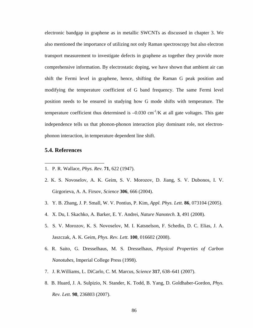
electronic bandgap in graphene as in metallic SWCNTs as discussed in chapter 3. We
also mentioned the importance of utilizing not only Raman spectroscopy but also electron
transport measurement to investigate defects in graphene as together they provide more
comprehensive information. By electrostatic doping, we have shown that ambient air can
shift the Fermi level in graphene, hence, shifting the Raman G peak position and
modifying the temperature coefficient of G band frequency. The same Fermi level
position needs to be ensured in studying how G mode shifts with temperature. The
temperature coefficient thus determined is –0.030 cm-1/K at all gate voltages. This gate
independence tells us that phonon-phonon interaction play dominant role, not electron-
phonon interaction, in temperature dependent line shift.
5.4. References
1. P. R. Wallace, Phys. Rev. 71, 622 (1947).
2. K. S. Novoselov, A. K. Geim, S. V. Morozov, D. Jiang, S. V. Dubonos, I. V.
Girgorieva, A. A. Firsov, Science 306, 666 (2004).
3. Y. B. Zhang, J. P. Small, W. V. Pontius, P. Kim, Appl. Phys. Lett. 86, 073104 (2005).
4. X. Du, I. Skachko, A. Barker, E. Y. Andrei, Nature Nanotech. 3, 491 (2008).
5. S. V. Morozov, K. S. Novoselov, M. I. Katsnelson, F. Schedin, D. C. Elias, J. A.
Jaszczak, A. K. Geim, Phys. Rev. Lett. 100, 016602 (2008).
6. R. Saito, G. Dresselhaus, M. S. Dresselhaus, Physical Properties of Carbon
Nanotubes, Imperial College Press (1998).
7. J. R.Williams, L. DiCarlo, C. M. Marcus, Science 317, 638–641 (2007).
8. B. Huard, J. A. Sulpizio, N. Stander, K. Todd, B. Yang, D. Goldhaber-Gordon, Phys.
Rev. Lett. 98, 236803 (2007).
86

9. B. O¨ zyilmaz, P. Jarillo-Herrero, D. Efetov, D. A. Abanin, L. S. Levitov, P. Kim,
Phys. Rev. Lett. 99, 166804 (2007).
10. Ph. Avouris, Z. H. Chen, V. Perebeinos, Nature Nanotech. 2, 605–615 (2007).
11. C. Berger, Z. M. Song, T. B. Li, X. B. Li, A. Y. Ogbazghi, R. Feng, Z. T. Dai, A. N.
Marchenkov, E. H. Conrad, P. N. First, W. A. de Heer, J. Phys. Chem. B 108, 19912
(2004).
12. X. Li, W. Cai, J. An, S. Kim, J. Nah, D. Yang, R. Piner, A. Velamakanni, I. Jung, E.
Tutuc, S. K. Banerjee, L. Colombo, R. S. Ruoff, Science 324, 1312 (2009).
13. Y. M. Lin, C. Dimitrakopoulos, K. A. Jenkins, D. B. Farmer, H. Y. Chiu, A. Grill, P.
Avouris, Science 327, 662 (2010).
14. M. Y. Han, B. Ozyilmaz, B. Y. Zhang, P. Kim, Phys. Rev. Lett. 98, 206805 (2007).
15. L. Jiao, L. Zhang, X. Wang, G. Diankov, H. Dai, Nature 458, 877 (2009).
16. D. V. Kosynkin, A. L. Higginbotham, A. Sinitskii, J. R. Lomeda, A. Dimiev, B. K
Price, J. M Tour, Nature 458, 872–876 (2009).
17. Y.-W. Son, M. L. Cohen, S. G. Louie: Phys. Rev. Lett. 97, 216803 (2006).
18. K. T. Nguyen, M. Shim, J. Am. Chem. Soc., 131, 7103 (2009).
19. K. Kamaras, M. E. Itkis, H. Hu, B. Zhao, R. C. Haddon, Science 301, 1501 (2003).
20. J. S. Bunch, A. M. van der Zande, S. S. Verbridge, I. W. Frank, D. M. Tanenbaum, J.
M. Parpia, H. G. Craighead, P. L. McEuen, Science 315, 490 (2007).
21. D. Graf, F. Molitor, K. Ensslin, C. Stampfer, A. Jungen, C. Hierold, L. Wirtz, Nano
Lett. 7, 238 (2007).
22. P. Lespade, A. Marchard, M. Couzi, and F. Cruege, Carbon 22, 375 (1984).
87

23. F. M Koehler, A. Jacobsen, K. Ensslin, C. Stampfer, W. J. Strak, Small 6, 1125
(2010).
24. D. B. Farmer, R. Golizadeh-Mojarad, V. Perebeinos, Y.-M Lin, G. S. Tulevski,J. C.
Tsang, P. Avouris, Nano Lett. 9, 388 (2009).
25. S. Pisana, M. Lazzeri, C. Casiraghi, K. S. Novoselov, A. K. Geim, A. C. Ferrari F.
Mauri, Nature Mater. 6, 198 (2007).
26. M. Lazzeri, F. Mauri, Phys. Rev. Lett. 97, 266407 (2006).
27. H. E.Romero, N. Shen, P. Joshi, H. R. Gutierrez, S. A.Tadigadapa, J. O. Sofo, P. C.
Eklund, ACS Nano 2, 2037, (2008).
28. L.Liu, S. Ryu, M. R. Tomasik, E. Stolyarova, N. Jung, M. S. Hybertsen, M. L.
Steigerwald, L. E. Brus, G. W. Flynn, Nano Lett. 8 1965 (2008).
29. D. Abdula, T. Ozel, K. Kang, D. G. Cahill, and M. Shim, J. Phys. Chem. C 112,
20131 (2008).
30. I. Calizo, A. A. Baladin, W. Bao, F. Miao, C. N. Lau, Nano Lett. 7, 2645 (2007).
31. N. Bonini, M. Lazzeri, N. Marzari, F. Mauri, Phys. Rev. Lett. 99, 176802 (2007).
32. A. Gaur and M. Shim, Phys. Rev. B 78, 125422 (2008).
88

5.5. Figures
Γ K (DP)
Figure 5.1: Electronic dispersion for graphene near the 6 corners of 2D Brillouin zone. Valence band and conduction band touch at DP (or K point).
89

1300 1400 1500 16000
200
400
600
500C
750CIn
tens
ity (a
.u)
Raman shift (cm-1)
2700 2600
Figure 5.2: Left panel: Raman spectra of graphene before (bottom spectrum) and after reaction with BBDT at indicated temperatures. The appearance of D band indicates defect formation in graphene. Right panel: Raman 2D band of graphene before functionalization. Its single, sharp Lorentzian lineshape confirms single layer graphene was used in the experiments.
1250 1300 1350 1600 17000
1000
2000
3000
4000
5000
D'G
D
Inte
nsity
(a.u
)
Raman shift (cm-1)
Figure 5.3: Raman spectra at different positions on graphene surface. D band appears at every spots and D- to G-band integrated intensity ratio varies from spot to spot. The top spectrum was collected at graphene edge and it exhibits highest degree of defect, indicating high reactivity of graphene edge.
90

-1.0 -0.5 0.0 0.5 1.0
0.0000001
0.0000002
0.0000003
0.0000004
0.0000005
0.0000006
0.0000007
750C
500C
Ids
(A)
Vg (V)
Figure 5.4: Transfer characteristic of graphene device before and after reaction with BBDT at indicated temperatures, corresponding to figure 5.2. 4-BBDT exposure does not significantly alter the current at the neutrality point (the minimum current) or drastically change the gate dependence of the device. There is only a positive shift of DP after the reaction, indicating p-type doping from BBDT as expected [21].
91

1500 1550 1600 16500
140
280
420
560K
471K
387K
278K
Inte
nsity
(a.u
)
Raman shift (cm-1)
2500 2600 2700 28000
200
400
600
800
1000
560K
471K
387K
278K
Inte
nsity
(a.u
)
Raman shift (cm-1)
Figure 5.5: Raman G band (upper) and 2D band (lower) of graphene at indicated temperatures and all spectra are collected when the Fermi level is at the DP. Frequency redshift is obvious for both features. The solid line guides the eyes.
92

-40 -20 0 20 401576
1580
1584
1588
1592
G b
and
Freq
uenc
y (c
m-1)
Vg (V)
Figure 5.6: Gate dependence of G band frequency at different temperatures: 298 K, 387 K, 471 K, and 560 K (from top to bottom curve) and during the first (black) and second (gray) heating process. The softening of G band phonon when the Fermi level is near the DP due to the presence of Kohn anomaly occurs at all four temperatures.
93
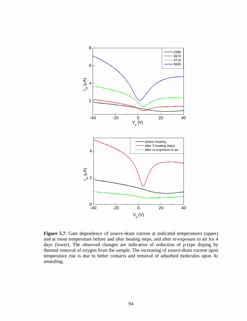
-40 -20 0 20 40
2
4
6
8
I ds (μ
A)
Vg (V)
298K 387K 471K 560K
-40 -20 0 20 400
2
4
I ds (μ
A)
Vg (V)
before heating after 3 heating steps after re-exposure to air
Figure 5.7: Gate dependence of source-drain current at indicated temperatures (upper) and at room temperature before and after heating steps, and after re-exposure to air for 4 days (lower). The observed changes are indicative of reduction of p-type doping by thermal removal of oxygen from the sample. The increasing of source-drain current upon temperature rise is due to better contacts and removal of adsorbed molecules upon Ar annealing.
94
300 350 400 450 500 550 600
0.8
1.2
1.6
2.0
I ds a
t the
DP
(μA)
Temperature (K)
1st heating 2nd heating 3rd heating
Figure 5.8: Source-Drain current at the DP of graphene device during the first, second, and third heating steps as a function of temperature.
95

-40 -20 0 20 40
1580
1584
1588
1592
560K
471K
387K
298K
G b
and
freqe
ncy
(cm
-1)
Vg (V)
Figure 5.9: The repetition of gate dependence of G band frequency at indicated temperatures during the subsequent cooling (black) and heating (gray) processes after the first heating.
300 350 400 450 500 550 600
1578
1581
1584
1587
G b
and
frequ
ency
(cm
-1)
Temperature (K)
Figure 5.10: Temperature dependence of G band frequency at zero gate voltage when the Fermi level is at the DP during the second (black dots) and third heating steps (black squares) and when it is not ensured (gray).
96

-40 -20 0 20 40-0.04
-0.03
-0.02
-0.01
0.00
Tem
pera
ture
coe
ffici
ent (
cm-1/K
)
Vg (V)
Figure 5.11: Temperature coefficient of G band frequency remains almost independent of gate voltage, indicating the minor role of electron-phonon coupling.
200 300 400 500 600
1580
1584
1588
1592
ωG = -0.03T + 1597.5G b
and
frequ
ency
(cm
-1)
Temperature (K)
Figure 5.12: Temperature dependence of G band frequency of graphene at the DP. The same value of temperature coefficient α, -0.03 cm-1/K, confirms the previous result extracted from figure 5.10.
97

-40 -20 0 20 40
8
10
12
14
16
18
20
22
G b
and
linew
idth
(cm
-1)
Vg (V)
298K 387K 471K 560K
350 525
9
10
11
G b
and
linew
idth
(cm
-1)
Temperature (K)
(c)
(a)
(b)
200 300 400 500 60015
16
17
18
19
20
21
G b
and
linew
idth
at D
P (c
m-1)
Temperature (K)
Figure 5.13: (a) Gate dependence of G band linewidth at indicated temperatures. The arrows represent the temperature dependence at different Fermi levels. (b) The decrease of G band linewidth at neutral charged state upon temperature rise with fitted curve obtained from reference 31. (c) The increase of G band linewidth at Vg = 40V where Fermi level is well above the DP because electron-phonon coupling is weaken and phonon-phonon interaction becomes more important.
98

-40 -20 0 20 402624
2628
2632
2636
2640
2644
2648
298K
387K
471K
560K2D
ban
d fre
quen
cy (c
m-1)
Vg (V)
(a)
-40 -20 0 20 40
2625
2630
2635
2640
560 K
471 K
387 K
298 K
2D b
and
frequ
ency
(cm
-1)
Vg (V)
(b)
-40 -20 0 20 40-0.06
-0.05
-0.04
-0.03
-0.02
-0.01
0.00
Tem
pera
ture
coe
ffici
ent (
cm-1/K
)
Vg (V)
(c) Figure 5.14: Gate dependence of 2D band frequency during the first (gray) and second heating steps (black) (a) and the second and third heating steps (b) and of temperature coefficient of 2D band frequency (c). The temperature coefficient of 2D mode is –0.05 cm-1/K and also nearly independent of gate voltage.
99

-40 -20 0 20 4028
30
32
34
298K
560K
2D b
and
linew
idth
(cm
-1)
Vg (V)
(a)
(b)
300 400 500 600
27
28
29
30
31
32
2D b
and
linew
idth
at t
he D
P
T (K)
1st heating 2nd heating 3rd heating
Figure 5.15: The dependence of 2D band linewidth on gate voltage at 298K and 560K (a) and on temperature during several heating steps (b). 2D band linewidth broadens upon heating as expected from phonon-phonon interaction. However, it broadens only 2 cm-1 from room temperature to 560K.
100

CHAPTER 6
CONCLUSIONS Single-Walled Carbon Nanotubes (SWCNTs) have been one of the most intensively
studied materials. Although it is the wide range of applications of CNTs that attracts most of the
media limelight, SWCNTs themselves offer unique opportunity to explore fundamental science of
quasi-1D conductors and semiconductors. In addition, because of their single-atomic-layer
structure, SWCNTs are extremely sensitive to environmental interactions of which
charge transfer and defect formation are the most notable effects. Among a number of
microscopic and spectroscopic methods, Raman spectroscopy is a widely used technique to
characterize physics and chemistry of CNTs. By utilizing simultaneous Raman and electron
transport measurements along with polymer electrolyte top gating, this dissertation focuses on
studying charging and defects in metallic (chapters 2 and 3) and semiconducting (chapter 4)
SWCNTs at the single nanotube level. These studies have also been investigated in single layer
graphene, the building block of SWCNTs, and have been discussed in chapter 5 of this work.
Electron-phonon interaction is critical for several important properties of CNTs,
including electrical transport, superconductivity, and optical transitions. The interaction
between electrons and phonons is also important factor in Raman scattering, affecting
Raman intensity, frequency, and linewidth. In turn, inelastic scattering can measure
electron-phonon coupling. Among various Raman features of SWCNTs, the broad and
asymmetric Fano lineshape in Raman G band has received much attention as it gives rise
to a striking difference between G band feature of semiconducting and metallic
SWCNTs. Being able to control charging degree in metallic SWCNTs, the evolution of
the G band spectra of single metallic SWCNTs with Fermi level shift has been examined.
Appearance of broad and asymmetric peak (LO phonon spectrum) at the Dirac point
101

indicates that the Fano component is intrinsic to single metallic SWCNTs and arises from
coupling between phonon and real vertical electronic excitations (or Kohn anomaly). The
Fermi level shift far away from the Dirac point changes the Fano lineshape to narrow
Lorentzian as there are no longer electronic states available for proper momentum and
energy changes in the electron-phonon scattering. Therefore, while the Fano lineshape is
a signature of metallic SWCNTs with the Fermi level close to the Dirac point, Lorentzian
is not necessarily indicative of semiconducting SWCNTs. Furthermore, all G modes
soften and broaden at the Dirac point, not only the LO mode as predicted by theoretical
calculation, and this has been discussed in light of defect formation.
While G band softening is symmetric for electron and hole doping, defect related
D-band shows monotonic dependence on the Fermi level shift. Electron-phonon
interaction plays a minor role for the D-band phonon. D-band frequency decreases when
electrons are injected into the antibonding states, resulting in an expansion of C-C bonds,
and increases when holes are injected to bonding states, causing bond contraction.
Although charging dependence of G-band and D band are different, the D-to G-band
integrated intensity ratio is indicative of defect degree in SWCNTs. Therefore the
broadening of G band at the Dirac point needs to be taken into account in order to
validate the use of the ratio for metallic SWCNTs.
By systematically introducing covalent defects by reaction with 4-bromobenzene
diazonium tetrafluoroborate at different concentrations, we have examined how electrical
characteristics and charging dependent Raman G-band phonon softening in individual
metallic SWCNTs are influenced by defect formation. In addition to decreasing electrical
conductance with increasing on/off current ratio eventually leading to semiconducting
102
behavior, adding covalent defects reduces the degree of softening and broadening of
longitudinal optical (LO) phonon mode of the G-band near the Dirac point. On the other
hand, the transverse optical (TO) mode softening is enhanced by defects. Softening of
both LO and TO modes may be expected due to covalent defects changing hybridization
of C atoms from sp2 to sp3 resulting in longer average bond lengths. However, LO mode
exhibits stiffening rather than softening because it is already softened via coupling of the
phonon with conduction electron excitations and the removal of this effect is the
dominant change. These observations imply that reported experimental LO mode
frequencies may be higher than the intrinsic frequencies due to the presence of physical
disorder, which is observed via measurable D-band intensities in majority of individual
metallic SWCNTs.
Raman spectroscopy is utilized as a metrology tool not only for metallic SWCNTs
but also for semiconducting SWCNTs. LO phonon in semiconducting SWCNTs also
softens when the Fermi level is between the first two van Hove singularities (vHs). This
process occurs by phonon-virtual electron hole-pair excitation coupling, unlike metallic
SWCNTs where actual carrier excitation occurs. In addition, LO linewidth broadens
significantly near vHs, in contrast with the narrowing in metallic nanotubes and with
theoretical prediction. The linewidth increasing is possibly inhomogeneous broadening
due to spatial difference of charge density. Charging dependence of LO mode remains
nearly unchanged upon introduction of covalent defects formed through reaction with 4-
bromobenzene diazonium tetrafluoroborate.
Doping single layer graphene, the building block of SWCNTs, by chemical and
electrostatic means has also been discussed in chapter 5 of this dissertation. The former is
103

carried out also by using 4-bromobenzene diazonium tetrafluoroborate. While 4-BBDT
causes p-doping of graphene, it does not help to open an electronic gap as in metallic
SWCNTs. Different reaction conditions or functional groups are recommended to
introduce a bandgap in graphene. Electrostatic doping of graphene at different
temperatures demonstrates the importance of ensuring the Fermi level in studying
temperature dependence of G band frequency. It also has been shown that contribution of
electron-phonon coupling to G peak position shift upon temperature change is negligible
and phonon-phonon interaction is dominating the line shift.
In short, simultaneous Raman spectroscopy and electrical measurement has been
proven to be a powerful combination of characterization techniques in studying SWCNTs
and graphene. It has revealed several important physical properties of the 1D and 2D
materials. Furthermore, it has helped to established background for potential carbon-
based electronic applications. The results described in this dissertation contribute to
progress in realizing carbon-based electronics.
.
104