chemical imaging using infrared photo-thermal ... imaging using infrared photo-thermal...
TRANSCRIPT
Chemical Imaging using Infrared Photo-thermal Microspectroscopy
Robert Furstenberg*, Christopher A. Kendziora, Michael R. Papantonakis, Viet Nguyen and R. A. McGill
U.S. Naval Research Laboratory, Code 6365, 4555 Overlook Ave SW, Washington, DC 20375, USA
ABSTRACT
There is a growing need for new characterization techniques that can provide information about the chemical composition of surfaces and bulk materials with spatial resolution in the range of 1-10 microns. While FTIR micro-spectroscopy addresses this problem, the practical resolution limit is still only about 20 microns. Other well-established techniques at the nanometer are impractical at the micro-scale. Raman micro-spectroscopy provides adequate spatial resolution (~1 micron), but may not always be useful due to its low throughput and for samples with strong fluorescence. We are developing a non-contact and non-destructive technique that provides similar information as IR or Raman spectroscopy. It involves photo-thermal heating of the sample with a tunable quantum cascade laser (or other suitable infrared laser) and measuring the resulting increase in thermal emission by either an infrared detector or a laser probe in the visible spectral range. The latter case allows for further increase of the spatial resolution from ~10 microns to ~1 micron, at the right experimental conditions. Since the thermal emission signal from the surface is directly proportional to the absorption coefficient, by tuning the laser wavelength we directly measure the IR spectrum of the sample. By raster-scanning over the surface of the sample we can obtain chemical composition maps. We demonstrate this technique by imaging the surface of several different materials. We analyze the spatial resolution of our photo-thermal imaging system as well as discuss the conditions under which the spatial resolution can be further increased from the infrared far-field diffraction limit.
Keywords: Microspectroscopy, infrared, quantum cascade laser, QCL, photo-thermal, characterization, chemical imaging, hyperspectral
1. INTRODUCTION Currently, there are several characterization techniques for chemical imaging of samples with a wide range of achievable spatial resolution. However, these techniques are not always well suited for samples where the required spatial resolution is 0.1 - ~1 microns. For example, FTIR spectroscopy provides the chemical composition but without spatial information. While FTIR micro-spectroscopy addresses this problem, the practical resolution limit is limited to about ~20 μm (in the mid-infrared or fingerprint region from ~5-12microns). X-Ray mapping can achieve much higher resolution but provides elemental maps, though this is not very useful for the identification of organic compounds. On the other hand, well-developed imaging techniques at the nanometer scale (scanning probe microscopy (SPM), atomic force microscopy (AFM), transmission electron microscopy (TEM) and its variant TEM/EELS etc.) may be impractical at the micron-scale due to small scanning speeds and limited scan range and more importantly because they provide limited chemical information about the sample. The emerging technique of Raman micro-spectroscopy provides adequate spatial resolution (~1 μm), but may not always be useful due to its low throughput and in cases where strong fluorescence suppresses the weak Raman signature. Another promising AFM-based technique, now available as a commercial instrument (nano-IR by Anasys Inc.) can achieve spatial resolution of ~100nm but requires very thin microtomed samples. Therefore, it appears that there is room for more new chemical imaging techniques, especially ones that require no sample preparation and can be performed in a non-contact and non-destructive manner.
In this paper we present a novel chemical imaging technique based on infrared photo-therrmal spectroscopy that has the potential to generate chemical images of samples with a spatial resolution of ~1um (below the far-field diffraction limit of a mid-IR beam). *Email: [email protected]; Phone: 202-767-5947
Next-Generation Spectroscopic Technologies V, edited by Mark A. Druy, Richard A. Crocombe,Proc. of SPIE Vol. 8374, 837411 · © 2012 SPIE · CCC code: 0277-786X/12/$18 · doi: 10.1117/12.919574
Proc. of SPIE Vol. 8374 837411-1
Downloaded from SPIE Digital Library on 31 May 2012 to 132.250.22.5. Terms of Use: http://spiedl.org/terms
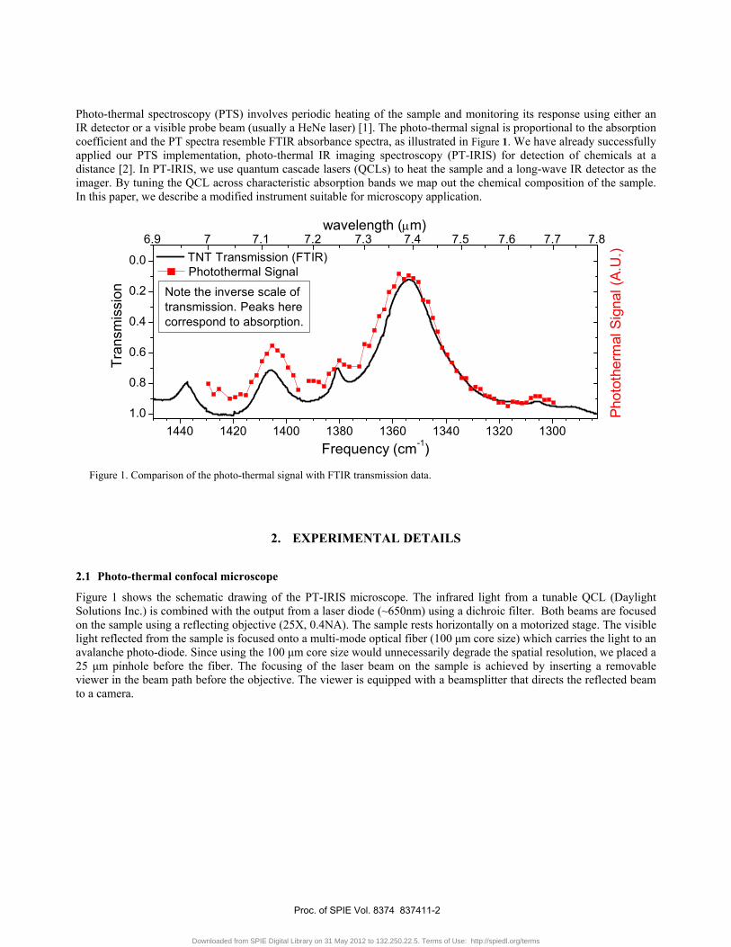
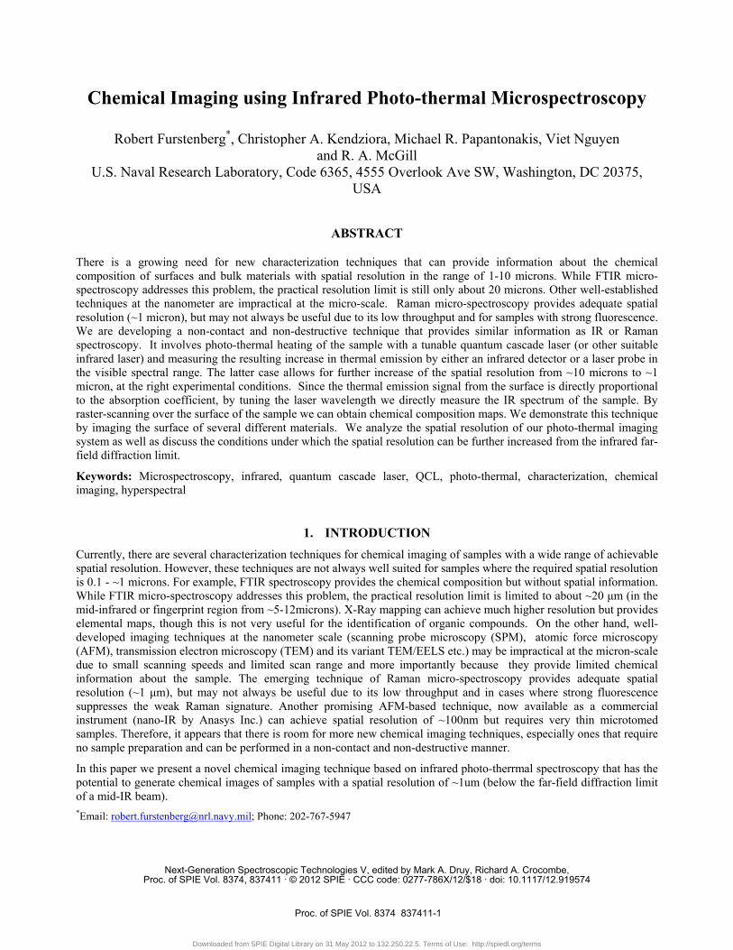
Photo-thermal spectroscopy (PTS) involves periodic heating of the sample and monitoring its response using either an IR detector or a visible probe beam (usually a HeNe laser) [1]. The photo-thermal signal is proportional to the absorption coefficient and the PT spectra resemble FTIR absorbance spectra, as illustrated in Figure 1. We have already successfully applied our PTS implementation, photo-thermal IR imaging spectroscopy (PT-IRIS) for detection of chemicals at a distance [2]. In PT-IRIS, we use quantum cascade lasers (QCLs) to heat the sample and a long-wave IR detector as the imager. By tuning the QCL across characteristic absorption bands we map out the chemical composition of the sample. In this paper, we describe a modified instrument suitable for microscopy application.
Figure 1. Comparison of the photo-thermal signal with FTIR transmission data.
2. EXPERIMENTAL DETAILS
2.1 Photo-thermal confocal microscope
Figure 1 shows the schematic drawing of the PT-IRIS microscope. The infrared light from a tunable QCL (Daylight Solutions Inc.) is combined with the output from a laser diode (~650nm) using a dichroic filter. Both beams are focused on the sample using a reflecting objective (25X, 0.4NA). The sample rests horizontally on a motorized stage. The visible light reflected from the sample is focused onto a multi-mode optical fiber (100 μm core size) which carries the light to an avalanche photo-diode. Since using the 100 μm core size would unnecessarily degrade the spatial resolution, we placed a 25 μm pinhole before the fiber. The focusing of the laser beam on the sample is achieved by inserting a removable viewer in the beam path before the objective. The viewer is equipped with a beamsplitter that directs the reflected beam to a camera.
1440 1420 1400 1380 1360 1340 1320 13001.0
0.8
0.6
0.4
0.2
0.0
6.9 7 7.1 7.2 7.3 7.4 7.5 7.6 7.7 7.8 TNT Transmission (FTIR)
Tran
smis
sion
Frequency (cm-1)
Note the inverse scale oftransmission. Peaks herecorrespond to absorption.
Pho
toth
erm
al S
igna
l (A.
U.)
Photothermal Signal
wavelength (μm)
Proc. of SPIE Vol. 8374 837411-2
Downloaded from SPIE Digital Library on 31 May 2012 to 132.250.22.5. Terms of Use: http://spiedl.org/terms
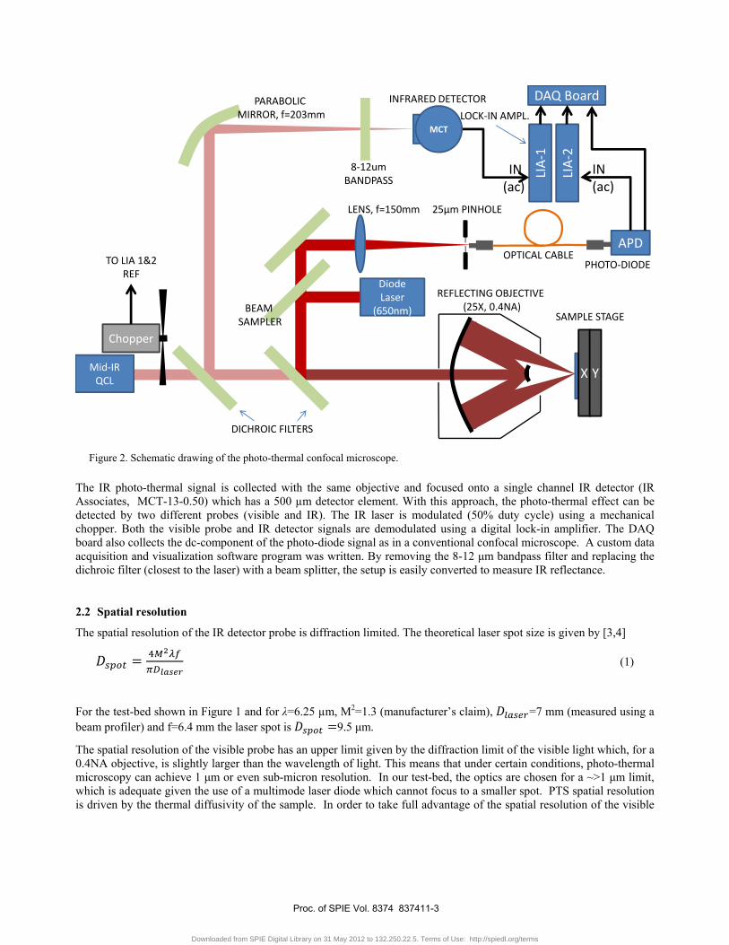
Figure 2. Schematic drawing of the photo-thermal confocal microscope. The IR photo-thermal signal is collected with the same objective and focused onto a single channel IR detector (IR Associates, MCT-13-0.50) which has a 500 µm detector element. With this approach, the photo-thermal effect can be detected by two different probes (visible and IR). The IR laser is modulated (50% duty cycle) using a mechanical chopper. Both the visible probe and IR detector signals are demodulated using a digital lock-in amplifier. The DAQ board also collects the dc-component of the photo-diode signal as in a conventional confocal microscope. A custom data acquisition and visualization software program was written. By removing the 8-12 μm bandpass filter and replacing the dichroic filter (closest to the laser) with a beam splitter, the setup is easily converted to measure IR reflectance.
2.2 Spatial resolution
The spatial resolution of the IR detector probe is diffraction limited. The theoretical laser spot size is given by [3,4]
(1)
For the test-bed shown in Figure 1 and for λ=6.25 µm, M2=1.3 (manufacturer’s claim), =7 mm (measured using a beam profiler) and f=6.4 mm the laser spot is 9.5 μm.
The spatial resolution of the visible probe has an upper limit given by the diffraction limit of the visible light which, for a 0.4NA objective, is slightly larger than the wavelength of light. This means that under certain conditions, photo-thermal microscopy can achieve 1 μm or even sub-micron resolution. In our test-bed, the optics are chosen for a ~>1 μm limit, which is adequate given the use of a multimode laser diode which cannot focus to a smaller spot. PTS spatial resolution is driven by the thermal diffusivity of the sample. In order to take full advantage of the spatial resolution of the visible
LIA
-1
LIA
-2
DAQ Board
APD
MCT
IN (ac)
IN (ac)
Chopper
TO LIA 1&2REF
X Y
8-12umBANDPASS
DiodeLaser
(650nm)
Mid-IRQCL
DICHROIC FILTERS
BEAM SAMPLER
PARABOLIC MIRROR, f=203mm
INFRARED DETECTOR
LOCK-IN AMPL.
PHOTO-DIODEOPTICAL CABLE
LENS, f=150mm 25μm PINHOLE
REFLECTING OBJECTIVE (25X, 0.4NA)
SAMPLE STAGE
Proc. of SPIE Vol. 8374 837411-3
Downloaded from SPIE Digital Library on 31 May 2012 to 132.250.22.5. Terms of Use: http://spiedl.org/terms
probe, the IRfrequency (fm
resolution is
ΔL=(4α/fm
Where α is surfaces whe
2.3 Diffract
In this modalof bright laselike data in rethe photo-thethe dichroichFigure 3 show
Figure 3. S
R excitation lasfmod) is a functgiven by the th
mod)0.5
the thermal dere the thermal
tion-limited ph
lity, the spatialers (as opposedeflection offer ermal signal (ph filter that sep
ws the schemati
chematic drawin
ser needs to be tion of not onlhermal diffusio
iffusivity of thcoupling in w
hoto-tehermal
l resolution is dd to dimmer incseveral potent
proportional to parates the exciic of the diffra
ng of the diffract
modulated at aly sample diffon length [5]
he sample. Foeaker, the therm
l microscope
diffraction limicoherent sourctial advantages the absorptionitation laser waction limited p
tion-limited pho
a high enough fusivity but als
or particular samal diffusion l
ited, just like ines) in a confocover traditiona
n coefficient) wavelengths from
photo-thermal m
to-tehrmal micro
frequency in oso geometry. T
amples consistlength is much
n FTIR microscal geometry anal FTIR micro-
we can also meam the collectiomicroscope.
oscope mode.
order to limit thThe worst-case
ting of mixtur small than the
s-spectroscopy.nd the ability to-spectroscopy.asure reflectancon wavelengths
hermal diffusioe value for the
es and particue one given by
. Even so, the o acquire abso Also, in additice by simply res by a beamspli
on. This e spatial
(2)
ulates on Eq. 2.
the use rbance-ion to eplacing itter.
Proc. of SPIE Vol. 8374 837411-4
Downloaded from SPIE Digital Library on 31 May 2012 to 132.250.22.5. Terms of Use: http://spiedl.org/terms
2.4 Sensing with the confocal visible probe (sub-diffraction limited mode)
Along with measuring the thermal emission (as described in the previous section), the photo-thermal effect can also be sensed by a visible laser probe that utilizes two phenomena that occur during the laser/sample interaction:
Thermo-optic effect
The thermo-optic effect is manifested in the periodic change in reflectance from the sample-air interface due to the periodic heating of the sample and air (through heat transfer from sample) and subsequent change in their refractive indices.
The reflectance coefficient at the sample-air interface is given by [6]
(4)
A thermally induced change in the indices of refraction will result in a change in reflectance given by 4 Δ (5)
where and are the thermo-optic coefficients for the sample and air, respectively.
Thermo-elastic effect
The thermo-elastic effect is based on the fact that the sample expands thermally in response to each IR laser pulse, thus modulating the sample position to which the confocal setup is sensitive; When heated, the focused laser spot on the sample becomes slightly out of focus and the photodiode is collecting less light. The beam radius away from a focused spot ( 0) is given by [3] 1 (6)
where is the beam waist radius at focus, the laser wavelength, and the distance from the focal spot along the optical axis. If the surface of the sample bulges up (due to heating) by Δ Δ (7)
where is the thermo-elastic coefficient, then the change in collected signal at the confocal aperture (or fiber optic input) of the photo-diode is Δ (8)
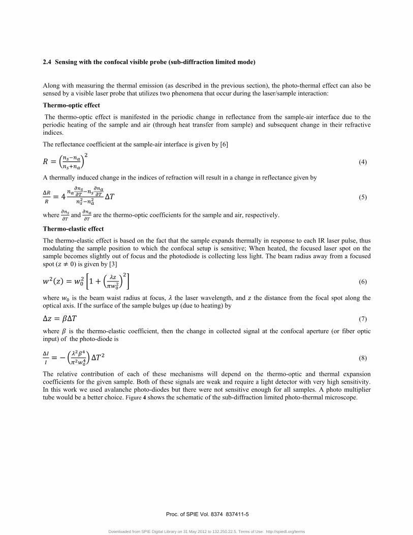
The relative contribution of each of these mechanisms will depend on the thermo-optic and thermal expansion coefficients for the given sample. Both of these signals are weak and require a light detector with very high sensitivity. In this work we used avalanche photo-diodes but there were not sensitive enough for all samples. A photo multiplier tube would be a better choice. Figure 4 shows the schematic of the sub-diffraction limited photo-thermal microscope.
Proc. of SPIE Vol. 8374 837411-5
Downloaded from SPIE Digital Library on 31 May 2012 to 132.250.22.5. Terms of Use: http://spiedl.org/terms
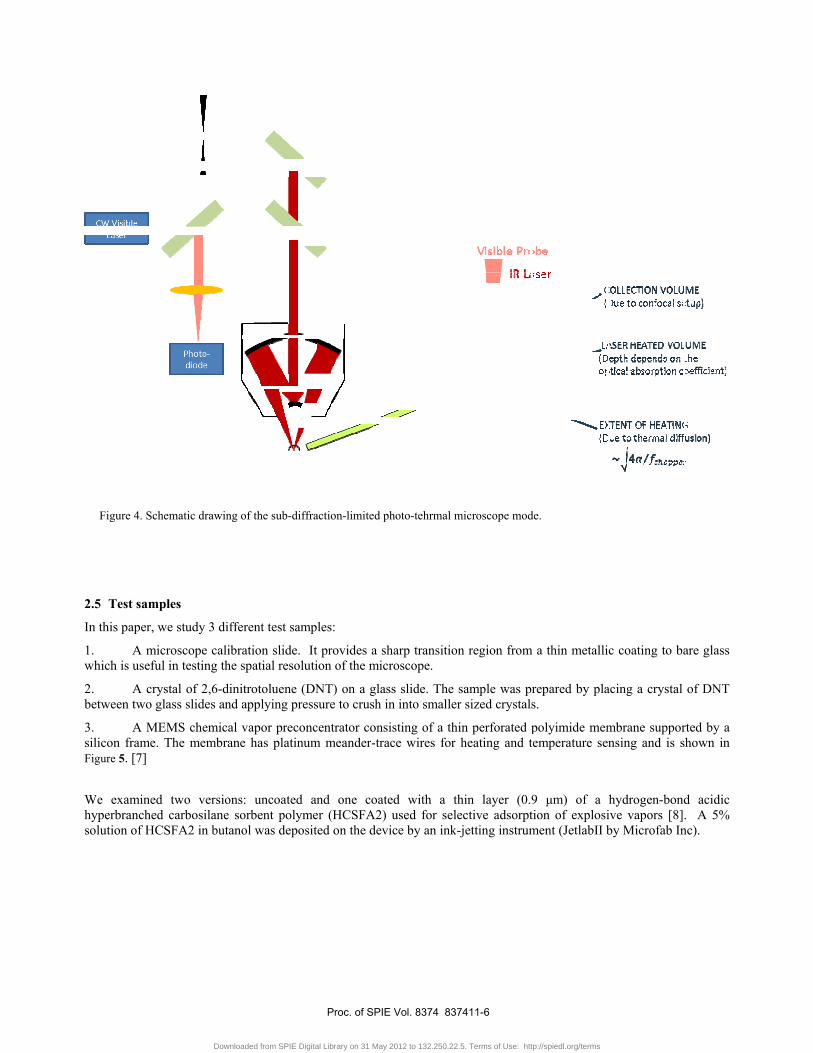
Figure 4. S 2.5 Test sam
In this paper,
1. A mwhich is usef
2. A cbetween two
3. A Msilicon frameFigure 5. [7]
We examinehyperbranchesolution of H
chematic drawin
mples
, we study 3 di
microscope califul in testing th
rystal of 2,6-dglass slides an
MEMS chemice. The membra
ed two versioed carbosilane
HCSFA2 in but
ng of the sub-dif
ifferent test sam
ibration slide. he spatial resolu
dinitrotoluene (nd applying pre
al vapor precoane has platinu
ons: uncoated e sorbent polymtanol was depo
ffraction-limited
mples:
It provides a ution of the mi
(DNT) on a glessure to crush
oncentrator conum meander-tr
and one coamer (HCSFA2sited on the de
d photo-tehrmal m
sharp transitioicroscope.
ass slide. The h in into smalle
nsisting of a thrace wires for
ated with a t2) used for selevice by an ink
microscope mod
on region from
sample was prer sized crystals
hin perforated pheating and t
thin layer (0.9lective adsorptk-jetting instrum
de.
m a thin metalli
repared by plas.
polyimide memtemperature sen
9 μm) of a tion of explosiment (JetlabII b
c coating to ba
acing a crystal
mbrane suppornsing and is s
hydrogen-bondive vapors [8]by Microfab In
are glass
of DNT
rted by a shown in
d acidic . A 5%
nc).
Proc. of SPIE Vol. 8374 837411-6
Downloaded from SPIE Digital Library on 31 May 2012 to 132.250.22.5. Terms of Use: http://spiedl.org/terms
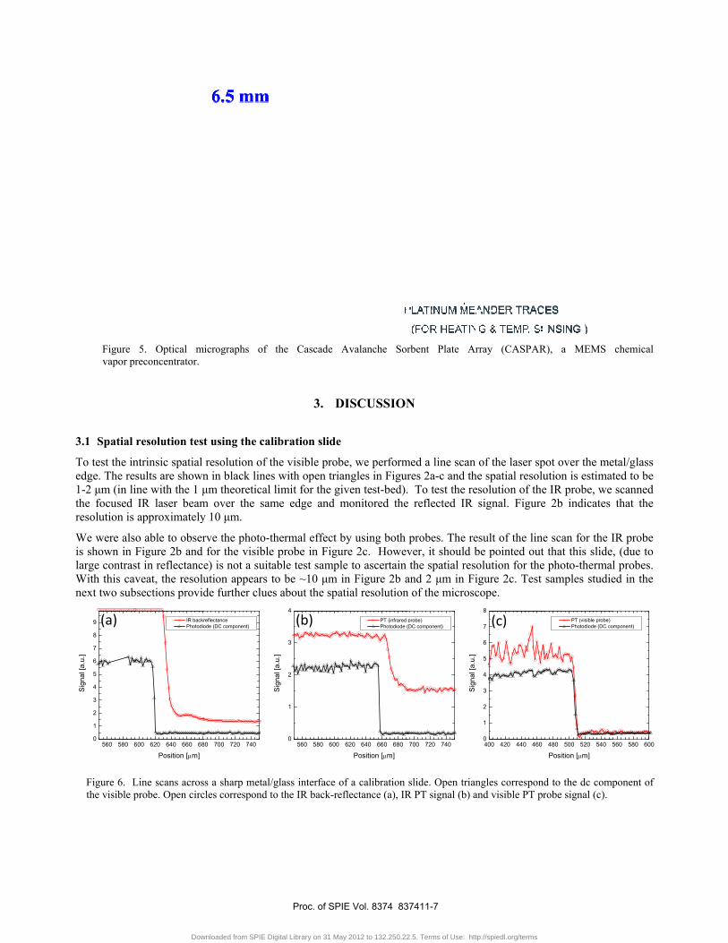
Figure vapor pr
3.1 Spatial
To test the inedge. The res1-2 μm (in lithe focused resolution is
We were alsois shown in Flarge contrasWith this cavnext two sub
Figure 6. L the visible p
560 580 60
1
2
3
4
5
6
7
8
9
Sign
al [a
.u.]
(a)
5. Optical mreconcentrator.
resolution test
ntrinsic spatial sults are shownne with the 1 μIR laser beamapproximately
o able to obserFigure 2b and st in reflectanceveat, the resolusections provid
Line scans acrosprobe. Open circ
600 620 640 660 68
Position [μm]
IR backr Photodio
icrographs of
t using the cal
resolution of tn in black linesμm theoretical m over the samy 10 μm.
rve the photo-tfor the visible
e) is not a suitaution appears tde further clue
s a sharp metal/cles correspond t
80 700 720 740
reflectanceode (DC component)
the Cascade
3. D
libration slide
the visible probs with open trialimit for the g
me edge and m
thermal effect be probe in Figuable test samplto be ~10 μm s about the spa
/glass interface oto the IR back-re
560 580 6000
1
2
3
4
Sign
al [a
.u.]
(b)
Avalanche Sor
DISCUSSION
e
be, we performangles in Figuriven test-bed). monitored the
by using both ure 2c. Howevle to ascertain in Figure 2b a
atial resolution
of a calibration eflectance (a), IR
620 640 660 680
Position [μm]
PT (infrared pPhotodiode (
rbent Plate Ar
N
med a line scan res 2a-c and th To test the re
reflected IR
probes. The rever, it should bthe spatial reso
and 2 μm in Fi of the microsc
slide. Open trianR PT signal (b) a
Sign
al [a
.u.]
700 720 740
probe)DC component)
rray (CASPAR
of the laser sphe spatial resoluesolution of thesignal. Figure
esult of the linebe pointed out olution for the igure 2c. Test cope.
ngles correspondand visible PT pr
400 420 440 4600
1
2
3
4
5
6
7
8
(c)
R), a MEMS
pot over the meution is estimate IR probe, we e 2b indicates
e scan for the Ithat this slidephoto-thermalsamples studie
d to the dc comprobe signal (c).
480 500 520 540 5
Position [μm]
PT (visible probe) Photodiode (DC co
chemical
etal/glass ted to be scanned that the
IR probe , (due to l probes. ed in the
ponent of
560 580 600
omponent)
Proc. of SPIE Vol. 8374 837411-7
Downloaded from SPIE Digital Library on 31 May 2012 to 132.250.22.5. Terms of Use: http://spiedl.org/terms
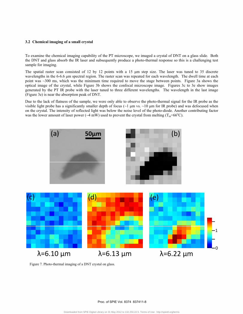
3.2 Chemical imaging of a small crystal
To examine the chemical imaging capability of the PT microscope, we imaged a crystal of DNT on a glass slide. Both the DNT and glass absorb the IR laser and subsequently produce a photo-thermal response so this is a challenging test sample for imaging.
The spatial raster scan consisted of 12 by 12 points with a 15 μm step size. The laser was tuned to 35 discrete wavelengths in the 6-6.6 μm spectral region. The raster scan was repeated for each wavelength. The dwell time at each point was ~300 ms, which was the minimum time required to move the stage between points. Figure 3a shows the optical image of the crystal, while Figure 3b shows the confocal microscope image. Figures 3c to 3e show images generated by the PT IR probe with the laser tuned to three different wavelengths. The wavelength in the last image (Figure 3e) is near the absorption peak of DNT.
Due to the lack of flatness of the sample, we were only able to observe the photo-thermal signal for the IR probe as the visible light probe has a significantly smaller depth of focus (~1 μm vs. ~10 μm for IR probe) and was defocused when on the crystal. The intensity of reflected light was below the noise level of the photo-diode. Another contributing factor was the lower amount of laser power (~4 mW) used to prevent the crystal from melting (Tm=66oC).
Figure 7. Photo-thermal imaging of a DNT crystal on glass.
50μm
λ=6.10 μm λ=6.22 μmλ=6.13 μm0
1
(a) (b)
(c) (d) (e)
Proc. of SPIE Vol. 8374 837411-8
Downloaded from SPIE Digital Library on 31 May 2012 to 132.250.22.5. Terms of Use: http://spiedl.org/terms
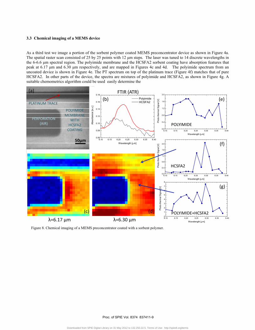
3.3 Chemical imaging of a MEMS device
As a third test we image a portion of the sorbent polymer coated MEMS preconcentrator device as shown in Figure 4a. The spatial raster scan consisted of 25 by 25 points with 12 μm steps. The laser was tuned to 14 discrete wavelengths in the 6-6.6 μm spectral region. The polyimide membrane and the HCSFA2 sorbent coating have absorption features that peak at 6.17 μm and 6.30 μm respectively, and are mapped in Figures 4c and 4d. The polyimide spectrum from an uncoated device is shown in Figure 4e. The PT spectrum on top of the platinum trace (Figure 4f) matches that of pure HCSFA2. In other parts of the device, the spectra are mixtures of polyimide and HCSFA2, as shown in Figure 4g. A suitable chemometrics algorithm could be used easily determine the
Figure 8. Chemical imaging of a MEMS preconcentrator coated with a sorbent polymer.
50μm
6.10 6.15 6.20 6.25 6.30 6.35 6.400.0
0.4
0.8
1.2
1.6
2.0
Phot
o-th
erm
al S
igna
l [V]
Wavelength [μm]
6.10 6.15 6.20 6.25 6.30 6.35 6.400.0
0.4
0.8
1.2
1.6
2.0
Phot
o-th
erm
al S
igna
l [V]
Wavelength [μm]
6.10 6.15 6.20 6.25 6.30 6.35 6.400
1
2
3
4
5
6
7
8
Phot
o-th
erm
al S
igna
l [V]
Wavelength [μm]λ=6.17 μm λ=6.30 μm
6.10 6.15 6.20 6.25 6.30 6.35 6.400.06
0.08
0.10
0.12
0.14
0.16
0.18
Polyimide HCSFA2
A
bsor
banc
e [a
.u.]
Wavelength [μm]
FTIR (ATR)
POLYIMIDE
HCSFA2
POLYIMIDE+HCSFA2
(a)
(b)
(c) (d)
(e)
(f)
(g)
PERFORATION(AIR)
POLYIMIDEMEMBRANE
WITHHCSFA2
COATING
PLATINUM TRACE
Proc. of SPIE Vol. 8374 837411-9
Downloaded from SPIE Digital Library on 31 May 2012 to 132.250.22.5. Terms of Use: http://spiedl.org/terms
4. CONCLUSIONS
We designed and built a photo-thermal microscope capable of chemical imaging with a resolution of ~10 µm. By using a visible light probe, this resolution can be further increased. However, we found that the visible probe signal is weak for certain samples and requires the samples to be flat. A better photo-diode and/or an interferometry-based light detection scheme will be used in the future to improve the photo-thermal signal strength.
We demonstrated our microscope on various test-samples. We were able to chemically image an organic crystal on a complex, IR-absorbing substrate. We also used the microscope to image the IR spectra of a sorbent polymer coated MEMS device. We showed that the coating process was successful and that the device surface was fully coated, with some thickness variation.
5. ACKNOWLEDGMENTS
This research was supported by funding from ONR/NRL.
REFERENCES
[1] Sell, J. A., [Photo-thermal Investigations of Solids and Fluids], Academic Press Inc., San Diego, 1-30 (1988). [2] Furstenberg, R., Kendziora, C. A., Stepnowski, J., Stepnowski, S. V., Rake, M., Papantonakis, M. R., Nguyen, V.,
Hubler, G. H., and McGill, R.A., “Stand-off detection of trace explosives via resonant infrared photothermal imaging”, Appl. Phys. Lett., 93, 224103 (2008).
[3] Young, M., [Optics and Lasers, 5th Ed.], Springer-Verlag, Berlin & Heidelberg & New York, 243 (2000). [4] Sun, H., “Thin lens equation for a real laser beam with weak lens aperture truncation”, Opt. Eng., 37(11) 2906–2913
(1998). [5] Carslaw, H. S., Jaeger, J. C., [Conduction of heat in solids], Clarendon Press, Oxford (1959) [6] Young, M., [Optics and Lasers, 5th Ed.], Springer-Verlag, Berlin & Heidelberg & New York, 221 (2000). [7] Martin, M., Crain, M., Walsh, K., McGill, R. A., Houser, E., Stepnowski, J., Stepnowski, S. V., Wu, H. D. and
Ross, S., “Microfabricated vapor preconcentrator for portable ion mobility spectroscopy”, Sensors And Actuators B - Chemical 126, 447-454 (2007).
[8] Higgins, B. A., Simonson, D. L., Houser, E. J., Kohl J. G. and McGill, R. A., “Synthesis and Characterization of a Hyperbranched Hydrogen Bond Acidic Carbosilane Sorbent Polymer”, J. Pol. Sci. Part A. 48, 3000-3009 (2010) .
Proc. of SPIE Vol. 8374 837411-10
Downloaded from SPIE Digital Library on 31 May 2012 to 132.250.22.5. Terms of Use: http://spiedl.org/terms