circuits and techniques for cell-based analog design
TRANSCRIPT

Circuits and Techniques for Cell-based Analog Design Automation in Advanced Processes
by
David M. Moore
A dissertation submitted in partial fulfillment of the requirements for the degree of
Doctor of Philosophy (Electrical Engineering)
in the University of Michigan 2018
Doctoral Committee: Associate Professor David D. Wentzloff, Chair Professor Sara A. Pozzi
Professor Dennis M. Sylvester Associate Professor Zhengya Zhang


ii
ACKNOWLEDGEMENTS
While I'd like to claim full credit for reaching this point, the reality is that my life has been
touched by many others that have left their marks on me, and led me to where I am today.
I'm thankful to every one of them, but here I'll thank those that have had the biggest impact
on this journey.
First, thanks to my advisor, Professor Dave Wentzloff. Dave was the reason I came to
Michigan, and has been a continual source of guidance, both in circuit design and otherwise.
I was incredibly lucky to have an advisor who cared so much about his students. I also need
to thank Professor Ben Calhoun from UVA, who first encouraged my interest in circuit design
and connected me to Dave. Although he has continually given me a hard time for "betraying
him" by going to Michigan, his influence was essential in bringing me to this point.
Thanks to all my past and present research group members in the WICS group at Michigan
who were both valuable collaborators and great friends. I think our group is unique in how
friendly everyone is, and I hope it continues to be that way. A special thanks to Muhammad
Faisal, who passed his research on to me, and was a great mentor as I learned the ropes.
Muhammad has become a great friend of mine, and a great supporter during the last year of
my PhD, which I completed in collaboration with his startup company, Movellus.
The experiences I gained through internships while at Michigan were absolutely invaluable
to my research. Cavium allowed a PhD student to take advantage of their resources in order
to try a new circuit design approach in a cutting-edge process, and taught me a great deal
iii
about PLL design, VLSI design, and the tapeout process in industry while I was there. This
was definitely a turning point for my research, and I'm grateful for it all.
My time at Movellus started as an internship but has become a journey of its own. I have to
give credit again to Muhammad; when he decided to start a company, I did not think in my
wildest dreams that it would get this far. He has been a great leader, and through the
experience I’ve learned a ton about the semiconductor industry. Jeff Fredenburg has been an
incredible boss, collaborator, and mentor, and I'm grateful that I've had the opportunity to
work with him. I've also been privileged to work with many more talented and extremely
motivated individuals, including Fish, Razan, Jason, Saeid, George, Gary, and Nash. Thanks to
all of them, and I look forward to continuing to with everyone at Movellus to achieve what
this research originally set out to do, and more.
Thanks to my brother Steven and all of my friends outside of Michigan, especially Dale, Matt,
Chris, Collin, and Amy. Your continual support over the years has helped keep me going, and
made sure I didn’t forget about life outside of my PhD. Thank you to my parents, Mike and
Carol Moore, for all your love and support, as well as all the advice you've given me over the
years. I’m definitely here in part because of the path you set me on, and the values you
instilled in me.
Finally, I could not have finished this program without the help of my wife, Chelsea Moore. I
wasn’t always easy, but you stuck with me every step of the way, encouraging me and
pushing me forward whenever I was stuck. Beyond being a support, you are my number one
inspiration. Thank you

iv
TABLE OF CONTENTS
ACKNOWLEDGEMENTS ..................................................................................................................................... ii
TABLE OF CONTENTS ........................................................................................................................................ iv
LIST OF FIGURES .................................................................................................................................................. vi
LIST OF TABLES.................................................................................................................................................... ix
ABSTRACT ............................................................................................................................................................... x
CHAPTER 1 Introduction ............................................................................................................................... 1
1.1. The Steady Advance of Digital IC Design ................................................................................ 2
1.2. Analog Challenges in Digital Chips ........................................................................................... 4
1.3. Attempts at Solving the Analog Problem ............................................................................... 6
1.4. Digitally-Assisted Cell-Based Analog Design ........................................................................ 9
1.5. Thesis Contributions ................................................................................................................... 12
CHAPTER 2 Modeling Techniques for Cell-Based Ring Oscillators ............................................ 15
2.1. Analytical Design Techniques for Cell-Based Ring Oscillators ................................... 15
2.2. Verification of Analytical Models ........................................................................................... 24
2.3. Static Timing Analysis for Ring Oscillators ........................................................................ 29
2.4. Proposed Static Timing Analysis Methodology ................................................................ 34
2.5. Static Timing Analysis Experimental Results .................................................................... 41
2.6. Conclusion ....................................................................................................................................... 45
CHAPTER 3 A Fast-Locking Cascaded PLL using Binary Search ................................................. 47
3.1. Proposed Architecture ............................................................................................................... 47
3.2. Measurement Results ................................................................................................................. 52

v
CHAPTER 4 A 5GHz Wide-bandwidth 14nm FinFET PLL for Processor Clocking ............... 55
4.1. Synthesizeable ADPLL Design ................................................................................................. 56
4.2. Measurement Results ................................................................................................................. 62
CHAPTER 5 Cell-based SERDES Circuits .............................................................................................. 66
5.1. Architecture Overview ............................................................................................................... 66
5.2. CDR Architecture .......................................................................................................................... 69
5.3. Physical Implementation of the CDR .................................................................................... 72
5.4. Receive Equalizer ......................................................................................................................... 73
5.5. Transmit Equalizer ...................................................................................................................... 74
5.6. Simulated Results ......................................................................................................................... 76
5.7. Measured Results ......................................................................................................................... 78
CHAPTER 6 Conclusions ............................................................................................................................. 83
6.1. Future Work ................................................................................................................................... 84
REFERENCES ....................................................................................................................................................... 87
vi
LIST OF FIGURES
Figure 1.1: Applications of Integrated Circuits [9] ................................................................................... 1
Figure 1.2: Typical Components of a Digital Processor.......................................................................... 2
Figure 1.3: The Typical Digital Design Flow [15] ..................................................................................... 3
Figure 1.4: DRC Complexity Increases Exponentially as Process Scaling Continues [22] ........ 5
Figure 1.5: A Typical ADPLL Architecture [24] ......................................................................................... 7
Figure 1.6: The Cell-Based Analog Design Flow [42] ........................................................................... 11
Figure 1.7: Typical Processor Blocks, with analog design automation from this research... 14
Figure 2.1: Structure of a cell-based oscillator, showing (a) block diagram, and (b) layout cell
placement. ............................................................................................................................................................. 16
Figure 2.2: Schematics of typical cells used in cell-based ring oscillators. .................................. 17
Figure 2.3: Noise reduction by duplicating oscillator cells. ............................................................... 23
Figure 2.4: Block diagram of a parameterized oscillator for the test chip................................... 25
Figure 2.5: Die micrograph of the oscillator test chip. ........................................................................ 25
Figure 2.6: Tuning range as a function of the number of tuning cells in each stage. ............... 26
Figure 2.7: Measurement results showing impact of oscillator parameters of various
performance metrics. ....................................................................................................................................... 27
Figure 2.8: Jitter models vs. experimental results ................................................................................ 28
Figure 2.9: Procedure for static timing analysis in ring oscillators. ............................................... 35
Figure 2.10: Cells typically used in cell-based ring oscillators. ........................................................ 36
Figure 2.11: Illustration of static timing analysis procedure for a single stage of the oscillator.
................................................................................................................................................................................... 39
Figure 2.12: Analysis of oscillator stage load on a cell-by-cell basis. When on m drivers out of
M are enabled, the load is effectively multiplied. .................................................................................. 40
Figure 2.13: Oscillator configurations used for testing. ...................................................................... 42

vii
Figure 2.14: Results for test case 1: Pseudo-differential DCO. 7 stages, 36 buffers per stage,
post-layout. All paths were analyzed. ........................................................................................................ 43
Figure 2.15: Results for test case 2: Singled-ended DCO. 7 stages, 36 buffers per stage, post-
layout. A sample of paths was analyzed. ................................................................................................... 44
Figure 2.16: Measured standard deviation in oscillator path timings for test case 2. ............ 45
Figure 3.1: Block Diagram of the Proposed Clock Generator ............................................................ 48
Figure 3.2: Principles of the dividerless fractional-N controller. .................................................... 50
Figure 3.3: DCO architecture and cell schematics. ................................................................................ 51
Figure 3.4: Binary search engine (BSE) behavior and measured lock time results. ................ 52
Figure 3.5: Measured phase noise spectrum. .......................................................................................... 53
Figure 3.6: Die Micrograph ............................................................................................................................. 54
Figure 4.1: Conventional Phase Domain Architecture ......................................................................... 56
Figure 4.2: Block Diagram of the Proposed PLL .................................................................................... 57
Figure 4.3: A Segment of the proposed phase-interpolated embedded TDC.............................. 58
Figure 4.4: DCO counter predivider detail. Automated hold-fixing is included. ....................... 59
Figure 4.5: Proposed DCO architecture. .................................................................................................... 60
Figure 4.6: Oscillator Auxiliary Cells. Coarse driver cell and fine capacitor cell. ...................... 60
Figure 4.7: Block diagram of on-chip data capture system. .............................................................. 61
Figure 4.8: Measured TDC nonlinearity. ................................................................................................... 62
Figure 4.9: Measured Phase Noise Spectrum with 5GHz Oscillator Frequency, divided to
2.5GHz. ................................................................................................................................................................... 63
Figure 4.10: Spectrum of the 2.5GHz output. .......................................................................................... 64
Figure 4.11: Test Bench used for measurements. ................................................................................. 64
Figure 4.12: Chip Micrograph........................................................................................................................ 65
Figure 5.1: Architecture of SERDES PLL with SSC. ................................................................................ 67
Figure 5.2: Detail of (a) phase interpolated embedded TDC and (b) SSC modulator, as well as
(c) SSC modulator output waveform. ......................................................................................................... 68
Figure 5.3: Architecture of Phase Interpolator-based CDR. .............................................................. 69
Figure 5.4: Circuit realization of the synthesizable phase interpolator. ...................................... 70
Figure 5.5: Control of PI nonlinearity through input slope tuning. ................................................ 71
Figure 5.5: Sampling comparator cell. ....................................................................................................... 72
viii
Figure 5.6: Typical CTLE Receiver. .............................................................................................................. 73
Figure 5.7: Cell-based CTLE circuit, with differential cells. ............................................................... 74
Figure 5.8: Transmitter block diagram. ..................................................................................................... 75
Figure 5.9: Transmitter cell-based output stage and cell detail. ..................................................... 76
Figure 5.10: Simulated Frequency Response of CTLE Receiver. Monte Carlo Results. .......... 77
Figure 5.12: Transmit Equalizer Output Waveform ............................................................................. 78
Figure 5.13: PLL Phase Noise and SSC Enabled Spectrum ................................................................. 79
Figure 5.14: SSC Frequency vs. Time .......................................................................................................... 79
Figure 5.15: Phase Interpolator Nonlinearity ......................................................................................... 81
Figure 5.16: Serial Link Die Photo ............................................................................................................... 82
ix
LIST OF TABLES
Table 2.1: Design Corners Tested ................................................................................................................ 42
Table 2.2: Results Summary .......................................................................................................................... 44
Table 3.1: Performance comparison with state-of-the-art work .................................................... 53
Table 4.1: Performance comparison of ring oscillator ADPLLs ....................................................... 65
Table 5.1: Power Consumption of System Components ..................................................................... 77
Table 5.2: PLL Performance Comparison ................................................................................................. 80
Table 5.3: Phase Interpolator Performance Comparison ................................................................... 81
x
ABSTRACT
Despite large advances in design automation of digital circuits to match the advance of
Moore’s law, Analog design techniques have remained relatively unchanged. Recently, cell-
based methodologies leveraging digital place and route tools have been explored in order to
accelerate the design of common analog circuit blocks, such as Phase Locked Loops (PLLs).
However, to date these designs have been implemented in older process nodes, and have
otherwise failed to target the needs of the high speed processors which dominate the
semiconductor industry.
This thesis examines that state of cell-based analog design automation, and presents new
techniques which will enable this approach to be used for analog blocks high speed
processors. First, analytical modeling was performed for cell-based oscillators, removing the
ad hoc circuit design process and enabling the number of iterative to design cycles to be
drastically reduced. Additional circuit techniques which can be leveraged in cell-based PLLs
were explored and two prototypes were implemented. In the first, a cascaded fast locking
frequency generation circuit was created in a 28nm SOI process. This achieves fractional-N
operation using an innovative controller, and design leverages binary search for fast locking.
In the second, a 5GHz wide-bandwidth PLL for processor clocking was created in a 14nm
FinFET process. This design achieves the widest output frequency range among synthesized
xi
PLLs. Finally, this design approach was extended to implement a phase interpolator for a
clock and data recovery (CDR) circuit, enabling a fully synthesized CDR.

1
Over the past nearly seven decades, the integrated circuit has evolved from an experiment
in a Texas Instruments lab to the backbone of the modern information economy. From
massive data centers [1], [2], to ubiquitous smart phones [3], to the smallest remote sensors
[4], [5], modern integrated circuits touch nearly every aspect of our lives. Modern processors
and Systems on Chip (SoCs) can contain billions of transistors, and represent a balance of
performance, power consumption, connectivity, and other abilities [6], [7]. Figure 1.1 shows
the various end-market applications which drive the more than $300 billion dollar
semiconductor industry [8].
Figure 1.1: Applications of Integrated Circuits [9]
CHAPTER 1
Introduction
2
A typical digital processor is shown in Figure 1.2. It consists of one or more cores or other
logic components, which are produced through an automated design process from a logic
description. These cores are attached to an on-chip memory which can be automatically
generated using a memory compiler. These represent the core digital components of the
processor, but they are surrounded by several analog circuits which contribute to the
processors final operation. Clock generation, voltage regulation, and high speed I/O are all
commonly needed on-chip in high speed processors [10]. SoCs may require additional analog
peripherals such as communication radios [11], [12]. For all of these additional analog
blocks, the design process is still largely done without automation.
Processor
Processor Cores
Memory
Serial I/Os
Clocking
Power Mgmt
Custom Design
Automated Design
Figure 1.2: Typical Components of a Digital Processor
1.1. The Steady Advance of Digital IC Design
Moore’s law process scaling has continued to drive the performance of digital devices
forward, enabling increasingly advanced applications [13]. These increasing complex digital
3
designs are enabled by increasingly powerful digital electronic design automation (EDA)
tools [14]–[16]. A typical digital EDA flow is shown in Figure 1.3. Digital designers describe
their design using a hardware description language (HDL) to model the logic. Constraints are
applied to the physical implementation to ensure that the resulting synchronous circuit can
operate at the intended frequency and under the intended conditions. The designer inputs
are then fed to a synthesis tool such as Synopsys’ Design Compiler, which will convert the
logic description to a circuit made of logic gates from a standard cell library. Finally, this
structural circuit description in physically implemented using a place and route tools such
as Cadence’s Innovus. These so-called “back end” tools will attempt to iteratively optimize
the design until it meets all timing constraints, yielding a passing design. This design
methodology is what allows processors with billions of transistors to be successfully
developed in a relatively short timeframe.
Figure 1.3: The Typical Digital Design Flow [15]
4
1.2. Analog Challenges in Digital Chips
While Moore’s law and digital EDA have enabled huge advances in digital circuits, the same
cannot be said for the analog support circuits that these processors and SoCs rely on. The
power and delay benefits that process scaling brings to digital circuits bring many penalties
with them to analog circuits. For one, smaller geometries typically result in increased
mismatch, and increased mismatch means that creating functioning analog circuits requires
substantially more effort [17]. Analog designers may be forced to use larger devices or
include calibration mechanisms [18], [19]. Scaled processes also frequently have increased
excess device noise and lower supply voltages which directly impact the noise performance
of analog circuits. And although bandwidth increases, lower gain of scaled processes makes
the design of many traditional analog blocks difficult. Finally, the availability of analog
models for transistors in a process typically lags the availability of digital models,
complicating the circuit design of analog blocks in new process nodes.
Analog design also faces numerous challenges not faced in digital design from the physical
design perspective, which is the drawing of the transistors and interconnect. In order to
achieve continued process scaling, in particular for FinFETs, technologies such as double and
triple patterning have been employed to print the small features [20], along with additional
factors such as quantized device sizes [21]. Additionally, layout dependent effects (LDE) can
drastically alter device performance beyond normal parasitic effects, providing another set
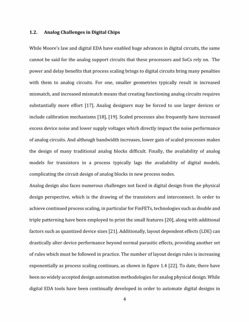
of rules which must be followed in practice. The number of layout design rules is increasing
exponentially as process scaling continues, as shown in figure 1.4 [22]. To date, there have
been no widely accepted design automation methodologies for analog physical design. While
digital EDA tools have been continually developed in order to automate digital designs in
5
spite of these increases in rules, the manual human-in-the-loop layout used in analog design
has led to a dramatic increase in physical design time. Additionally, many analog circuits
require the use of additional backend components such as MIMCAPs and inductors which
are not used in digital design, complicating integration. Finally, because there is no tool for
translating a behavioral description of an analog circuit to a physical netlist, which is
common-place in the digital design flow, porting an analog design from one process node to
another often involves a complete manual redesign from scratch.
Figure 1.4: DRC Complexity Increases Exponentially as Process Scaling Continues
[22]

6
1.3. Attempts at Solving the Analog Problem
Multiple approaches have been attempted in academia and industry to alleviate the many
issues with analog design highlighted here. Some have found commercial success in limited
applications, while others have not. A broad overview of two major ideas in solving analog
design automation problems is given below.
1.3.1. Digitally-Assisted Analog
Much attention has been given to an approach called “digitally-assisted analog”, where
digital components are used to enhance the functionality of analog circuits [23]. Highly
digital architectures, which replace analog sub-blocks with equivalent digital components
are used as a means to reduce susceptibility to analog performance problems, and to
increase design reusability. An example is the all-digital phase locked loop (ADPLL), such as
that shown in Fig. 1.5 [24]. In a typical ADPLL, the analog phase detector, loop filter, and
voltage controlled oscillator (VCO) blocks are replaced with a time to digital converter (TDC),
digital loop filter (DLF), and digitally controlled oscillator (DCO). This allows the number of
analog components to be reduced, shrinking and improving the design. A similar approach
of block substitution has been applied to other analog blocks, such as some radio
transceivers [25], [26]. Another approach is the digital linearization of analog nonlinearities.
In this case, a digital function is applied to a signal before it goes to or after it comes from the
analog domain, in order to cancel the nonlinearity of analog components [27].
Overall, digitally-assisted analog has yielded substantial benefits in a number of areas, and
has been widely adopted by industry. However, while it is effective for the blocks which
become completely digital, such as filters, in reality the TDC and DCO are mixed-signal

7
blocks, which are then designed and laid out through the same custom process as their
analog predecessors. This means that the suffer from the same drawbacks, to a large extent.
In addition, using digital control on an analog block produces another drawback in the form
of quantization noise. Quantization noise is a performance degradation that occurs due to
the finite resolution of digital circuits, and contributes directly to the phase noise of ADPLLs,
both in the TDC and DCO [28].
Time -to-
Digital
DigitalLoop Filter
Divider
ref(t) out(t)
DCO
Figure 1.5: A Typical ADPLL Architecture [24]
1.3.2. Analog Design Automation
In addition to work on digitally-assisted analog, a substantial amount of effort has been
devoted to analog design automation over the past several decades. These strategies include
analog standard cells, predetermined or derived analytical models, automatic optimization,
and genetic algorithms, among others. The following is a short history.
In the late 1980s, following the development of the first EDA tools for digital design,
researches started exploring the idea of creating analog standard cell libraries, which were
intended to contain many typical analog functions, such as amplifiers and data convertors
8
[29], [30]. The elements of these cell libraries would be relatively complicated analog blocks,
such as operational amplifiers, passive arrays, filters, oscillators, voltage references, with
some even specifying data converters as elements. However, while assembling a library of
digital cells which can implement most of the desirable functionality of digital circuits is
straightforward, the same is not true for analog design. The variation in analog performance
parameters is much wider than in digital, and as process scaling continued to make analog
design more complicated, the idea of building larger analog functionality from a readily
available library became less and less realistic. Today this idea survives to an extent as the
analog IP market (e.g. TrueCircuits, Analogbits, Synopsis), which provides blocks which new
designs may be assembled from, but without any sort of automated synthesis.
An additional approach to analog automation has been the attempted use of analytical
equations in order to perform the automated generation of analog blocks. The most basic of
these are tools which would use specifications to perform sizing on fixed circuit schematics,
such as OPASYN [31], [32]. These tools would use predetermined analytical equations
derived from a specific circuit topology to determine circuit performance, then adjust device
sizes using convex optimization until the design specification was met. Later tools such as
OASYS broke the analog block into hierarchical components and then applied the
optimization [33]–[35]. This concept was expanded on by the next generation of tools in a
variety of directions. One class of tools continued focusing on analytical equations, using
design specified equations and more powerful optimization engines. However, this approach
never gained momentum due to the failure of analytical equations to accurately capture
important aspects of analog designs [36]. More successful tools leveraged commercial
simulators in the feedback loop in order to analyze performance. In the late 90s and early
9
00s, approaches such as using genetic algorithms to replicate analog designer intuition were
attempted [37]. However, many of these tools were not able to properly optimize across
layers of hierarchy, as is often required in analog design.
To date, while some analog design automation features have been absorbed into commercial
EDA tools, no complete solution has had significant success [38]–[40]. While existing tools
have been able to produce functional designs, they cover only a small portion of the analog
application space. These tools could only produce small blocks or a narrow class of systems,
meaning that outside of a few specific cases, designers were forced to fall back on custom
design [41]. Additionally, they were largely not portable across process, requiring
substantial engineering effort for every new process node that greatly hampered any
potential usefulness.
1.4. Digitally-Assisted Cell-Based Analog Design
Learning from previous attempts, a new approach for analog system design automation has
emerged that combines optimization with digitally-intensive architectures which we refer
to as digitally-assisted cell-based analog design.
Digitally-assisted cell-based analog design takes the idea of individually characterized circuit
cells from digital circuits, and applies it to analog design. However, in contrast with the
original analog standard cell libraries, the cells involved here are not intended to represent
individual units of analog functionality [29], [30]. Instead, digitally intensive architectures
are used to reduce the number of essential analog circuits which must be created. The
portions which must be analog are made tunable by breaking them into individual digitally
controlled tuning cells, which can be placed separately into a cell grid and later routed.

10
Digital tuning can then be accomplished either using calibration or closed loop feedback,
such as in a PLL, removing strict analog performance requirements from individual
elements. By leveraging the digital tools in this way, the automated solutions to process
scaling developed for digital circuits can be extended to analog circuits.
Part of the reason that this is now possible is because of an interesting trend that has
appeared in digital design, in parallel with the difficulty of analog design. While digital
performance continues to benefit from scaling, the actual design of digital circuits has grown
increasingly difficult for many of the same reasons as analog design. Increased process
variation, temperature sensitivity, interconnect parasitics, layout effects, DRC requirements,
and modeling complexity have all begun to limit digital design. Many of the assumptions of
the original digital tools are no longer valid, leading to an expanding range of tools and
models for various effects used in the design and verification of modern digital elements.
Digital design has in fact become closer and closer to analog design. This fact has motivated
the use of digital tools to perform more analog design functions. One method this has been
achieved with is the use of cell-based analog design.
An example of the cell-based analog design flow for ADPLLs is shown in Figure 1.6.
The design starts with specifications for the PLL such as output frequency tuning range and
jitter. From this, the required DCO and TDC resolutions are calculated to achieve the jitter
specification. One or more oscillator cells are designed or selected from a library in order to
create the first version of the oscillator. The digital synthesis and place and route flows are
used to generate the entire PLL design, using a parameterized Verilog description. The
performance of the oscillator is then measured (typically using SPICE simulations), and
compared to the specification. Based on the difference between the to, either oscillator
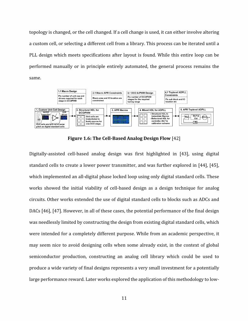
11
topology is changed, or the cell changed. If a cell change is used, it can either involve altering
a custom cell, or selecting a different cell from a library. This process can be iterated until a
PLL design which meets specifications after layout is found. While this entire loop can be
performed manually or in principle entirely automated, the general process remains the
same.
Figure 1.6: The Cell-Based Analog Design Flow [42]
Digitally-assisted cell-based analog design was first highlighted in [43], using digital
standard cells to create a lower power transmitter, and was further explored in [44], [45],
which implemented an all-digital phase locked loop using only digital standard cells. These
works showed the initial viability of cell-based design as a design technique for analog
circuits. Other works extended the use of digital standard cells to blocks such as ADCs and
DACs [46], [47]. However, in all of these cases, the potential performance of the final design
was needlessly limited by constructing the design from existing digital standard cells, which
were intended for a completely different purpose. While from an academic perspective, it
may seem nice to avoid designing cells when some already exist, in the context of global
semiconductor production, constructing an analog cell library which could be used to
produce a wide variety of final designs represents a very small investment for a potentially
large performance reward. Later works explored the application of this methodology to low-
12
power radios, using custom delay cells to build a ring oscillator [42], [48]. While this showed
the effectiveness of custom cells, it offers a limited application space, since the majority of
wireless standards require LC oscillators in order to meet phase noise specifications. Recent
research has showed that the strategy may be extensible to LC oscillators, although work is
early [49]. Additional work has extended this approach using custom cells to DACs, with
positive results [47].
1.5. Thesis Contributions
A broad application area for cell-based analog design is in clock generators and other timing
based circuits for digital processor applications. A common digital processor can feature as
many as 10 PLLs, with several different requirement sets [50], [51]. Additionally, these
circuits are often ring oscillator based, and may benefit from being tightly integrated with
the digital core. With the above in mind, this work explores methods to apply cell-based
analog design to the practical problems facing analog design for digital processors in
advanced nodes. The specific contributions of this work are as follows:
1. Modeling Techniques for Cell-Based Ring Oscillators
Two modeling techniques which take advantage of the structure of cell-based ring
oscillators are developed and explored. The first relies on the characterization of a
single oscillator fitting analytical equations to the measured data. The properties of
other oscillators made from the same cell are derived from this. The second technique
leverages static timing analysis to characterize a single oscillator cell, and accurately
predict frequency after automated layout. These techniques are addressed in Chapter
2.

13
2. A Fast-Locking Cascaded Frac-N PLL with a Binary Search Engine
A novel fractional-N PLL architecture based on two cascaded PLLs was implemented
entirely using the cell-based analog design flows. The PLL targets the 900 – 940 MHz
range, and utilizes a binary search algorithm in order to achieve extremely fast
locking time. Details of the architecture and cells used in this design are discussed in
Chapter 3.
3. A 5GHz Wide-Bandwidth FinFET PLL for Processor Clocking
A PLL specifically design for clocking a multicore high-performance processor was
developed in a 14nm FinFET process using the cell-based analog flow. Using a phase
domain architecture, 8MHz bandwidth was achieved. A high frequency target was
selected to allow division to achieve 50% duty cycle, while architectural innovations
allowed low jitter. The details of this design are presented in Chapter 4.
4. A Cell-based SERDES interface designed for SoC applications
Finally, future work for the proposed thesis will move beyond PLLs into another
analog block which is perhaps even more important to digital processors: high speed
SERDES I/O circuits. The cell-based analog flow will be used to develop a clock and
data recovery circuit, as well as the transmit and receive equalization circuit for a
SERDES transceiver with a multi-gigabit datarate. The details of this design will be
discussed in Chapter 5.
Across these contributions, a variety of architectures, circuits, and custom cell designs are
explored in order to best tackle the problem of automating analog design in high
performance processors. In tackling clock generation and SERDES, this work seeks to make
the automation picture in Figure 1.7 a reality.

14
Processor
Processor Cores
Memory
Serial I/Os
Clocking
Power Mgmt
Custom Design
Automated Design
Figure 1.7: Typical Processor Blocks, with analog design automation from this
research.
15
Previous work has shown that ADPLLs can be automatically designed using a cell-based ring
oscillator as a core [42], [44], [48], [52], [53]. Although the assembly of the overall circuit is
performed within the digital EDA flow, which alleviates the need for a substantial amount of
resources normally used in analog design, the design and verification of these circuits still
relies on SPICE simulations. For instance, designers must manually extract parasitic
capacitance and resistance after completing the EDA flow, and then simulate their design to
verify performance. Additionally, because these highly digital architectures may often
include many additional cells in the output from the digital tool, simulation times can be
longer than in the traditional analog case due to the large number of transistors in the design.
In this chapter we present two techniques which can be used to accelerate the design of cell-
based ring oscillators beyond what is possible using only SPICE simulations in the feedback
loop. The first is an analytical technique which can be used to produce an appropriate
starting point for optimization. The second is a numerical technique based on a new
application of static timing analysis (STA) in order to improve optimization times.
2.1. Analytical Design Techniques for Cell-Based Ring Oscillators
Developing a full physical library of oscillator cells, analogous to a standard cell library,
facilitates multiple designs by reusing and modifying Verilog only, with minimal or no new
CHAPTER 2
Modeling Techniques for Cell-Based Ring Oscillators

16
custom design. However, as a given design only tends to require between 3 and 4 varieties
of analog cells, physical cell design can potentially be postponed until rough oscillator design
is completed using the procedures described in this section along with estimated parasitics.
This section presents an analysis of these factors in the context of cell-based ring oscillators,
which can be used to efficiently produce oscillators with automated physical design. A block
diagram of such as oscillator is shown in Figure 2.1. Examples of typical current or capacitor
tuning cells are shown in Figure 2.2.
(a)
(b)
Figure 2.1: Structure of a cell-based oscillator, showing (a) block diagram, and (b)
layout cell placement.
VDD VDD VDD
M parallel buffers per stage
N stages
DCO Control

17
Single-Ended Current Cell
Pseudo-Differential Current Cell
inp
inn
outn
outp
enen
en
en
inp
inn
outn
outp
enen
en
en
in
en
in
en
Switched Capacitor Cell
=out
en
in
en
in
en
in out
en
in out
en
=out
en
in
en
in out
en
Figure 2.2: Schematics of typical cells used in cell-based ring oscillators.
In order to use automatically generated DCOs for high-performance frequency generation, it
is necessary to ensure that these oscillators meet center frequency, tuning range, and phase
noise requirements. This section presents an analysis of these factors in the context of cell-
based ring oscillators, which can be used to efficiently produce oscillators with automated
physical design. The following analysis assumes the use of any of the three cells from Figure
2.2, examining only the effects of combining fixed cells in various configurations. Specifically,
we examine the impact of the number of cells per stage and the number of oscillator stages
on the previously mentioned performance requirements.
2.1.1. Center Frequency and Tuning Range
Though every variety of ring oscillator has a slightly different collection of factors that affect
output frequency, all designs tend to possess a linear relationship with current consumption
and an inverse relationship with load capacitance in the oscillator. That is to say, for a generic
ring oscillator,
𝒇𝟎 = 𝒌
𝑰
𝑪
(2.1)

18
where 𝑘 is a process and circuit dependent constant, while 𝐼 and 𝐶 represent the “total
current” and “total capacitance” of the oscillator, respectively. Empirically, keeping a
common cell topology results in a relatively constant 𝑘, allowing the strength of a cell to be
described by the ratio of 𝐼 and 𝐶. While this model is simplified, it can be used to predict how
a modified oscillator will differ from a baseline design. Following this approach, a library of
oscillator cells can be characterized in a baseline case to determine I and C contributions,
then combined to achieve the target 𝑓0.
Tuning range analysis is tightly related to that for center frequency. Assuming current-cell-
based tuning allows (2.1) to be rewritten as
𝒇𝟎 = 𝒌
𝑰𝑩 + 𝒏𝑰𝒕𝒖𝒏𝒆𝑪𝑩 +𝑵𝑪𝒕𝒖𝒏𝒆
. (2.2)
Here, the 𝐼𝐵 and 𝐶𝐵 represent the baseline quantities, while 𝐼𝑡𝑢𝑛𝑒 and 𝐶𝑡𝑢𝑛𝑒 represent the
contributions of an individual tuning cell. Additionally, 𝑁 is the total number of current
tuning cells in the design, while 𝑛 is the number of enabled current cells.
The fractional tuning range of the oscillator is the fraction of the maximum frequency over
which the oscillator can be tuned, which can be written as
𝑻𝑹 = 𝟏 −
𝒇𝒎𝒊𝒏
𝒇𝒎𝒂𝒙. (2.3)
Combining this with (2.2) and simplifying (using 𝑛 = 0,𝑁 at 𝑓𝑚𝑖𝑛, 𝑓𝑚𝑎𝑥) yields
𝑻𝑹 =
𝑵
𝑵+ 𝑰𝑩 𝑰𝒕𝒖𝒏𝒆⁄. (2.4)
Thus, tuning range dependence on the number of tuning elements follows a nonlinear
characteristic that is dependent on only the ratio of base current to the tuning element
current. Once the maximum frequency target is met and the basics of the oscillator are
determined, the ratio can be calculated and an arbitrary tuning range can then be achieved

19
using (2.4). An expression for tuning using switched capacitors is similarly straightforward.
Assuming that a capacitor cell has on-capacitance 𝐶𝑜𝑛 and off-capacitance 𝐶𝑜𝑓𝑓, the
frequency of a switch-cap tunable oscillator is given by
𝒇𝟎 = 𝒌
𝑰𝑩𝑪𝑩 + 𝒏𝑪𝒐𝒏 + (𝑵 − 𝒏)𝑪𝒐𝒇𝒇
. (2.5)
Following the same approach as above, the tuning range is given by
𝑻𝑹 =
𝑵(𝑪𝒐𝒏 − 𝑪𝒐𝒇𝒇)
𝑪𝑩 +𝑵𝑪𝒐𝒏. (2.6)
The tuning resolution of the DCO is another important design specification because it affects
quantization noise introduced in a PLL [28]. Using the above approach, it is possible to derive
relationships between the desired resolution and the required tuning cell. For current based
tuning cells, it is desirable to closely match the 𝐼/𝐶 ratio of the cells to that of the oscillator
in order to avoid dramatically altering the maximum output frequency. Assuming this is the
case, the relationship of interest is
𝑪𝒕𝒖𝒏𝒆 =
𝚫𝒇
𝒇𝟎𝑪𝑩, (2.7)
where Δ𝑓 is the desired resolution. For capacitor based tuning, the 𝐼/𝐶 ratio will necessarily
be decreased, and thus this must be accounted when using these cells. The relationship in
this case is
𝚫𝑪 =
𝚫𝒇
𝒇𝟎𝑪𝑩, (2.8)
Where Δ𝐶 is the difference between the capacitance in the on and off states of the cell. The
influence of 𝐼𝑡𝑢𝑛𝑒 and 𝐶𝑡𝑢𝑛𝑒 on different aspects of the oscillator dictates the variety of cells
which are needed in a library.
20
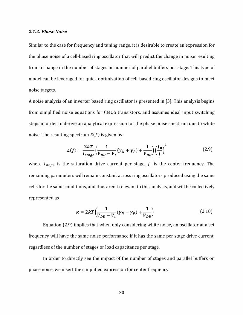
2.1.2. Phase Noise
Similar to the case for frequency and tuning range, it is desirable to create an expression for
the phase noise of a cell-based ring oscillator that will predict the change in noise resulting
from a change in the number of stages or number of parallel buffers per stage. This type of
model can be leveraged for quick optimization of cell-based ring oscillator designs to meet
noise targets.
A noise analysis of an inverter based ring oscillator is presented in [3]. This analysis begins
from simplified noise equations for CMOS transistors, and assumes ideal input switching
steps in order to derive an analytical expression for the phase noise spectrum due to white
noise. The resulting spectrum ℒ(𝑓) is given by:
𝓛(𝒇) =
𝟐𝒌𝑻
𝑰𝒔𝒕𝒂𝒈𝒆(
𝟏
𝑽𝑫𝑫 − 𝑽𝒕(𝜸𝑵 + 𝜸𝑷) +
𝟏
𝑽𝑫𝑫) (
𝒇𝟎𝒇)𝟐
(2.9)
where 𝐼𝑠𝑡𝑎𝑔𝑒 is the saturation drive current per stage, 𝑓0 is the center frequency. The
remaining parameters will remain constant across ring oscillators produced using the same
cells for the same conditions, and thus aren’t relevant to this analysis, and will be collectively
represented as
𝜿 = 𝟐𝒌𝑻(
𝟏
𝑽𝑫𝑫 − 𝑽𝒕(𝜸𝑵 + 𝜸𝑷) +
𝟏
𝑽𝑫𝑫) (2.10)
Equation (2.9) implies that when only considering white noise, an oscillator at a set
frequency will have the same noise performance if it has the same per stage drive current,
regardless of the number of stages or load capacitance per stage.
In order to directly see the impact of the number of stages and parallel buffers on
phase noise, we insert the simplified expression for center frequency

21
𝒇𝟎 =
𝑰𝒔𝒕𝒂𝒈𝒆
𝑴𝑪𝒔𝒕𝒂𝒈𝒆𝑽𝑫𝑫𝟐 (2.11)
Here, 𝑀 is the number of stages, and 𝐶𝑠𝑡𝑎𝑔𝑒 is the load capacitance per stage. this gives the
resulting expression for phase noise
𝓛(𝒇) =
𝜿𝑰𝒔𝒕𝒂𝒈𝒆
𝑴𝟐𝑪𝒔𝒕𝒂𝒈𝒆𝟐 𝑽𝑫𝑫
𝟒(𝟏
𝒇𝟐) (2.12)
From this equation, we can determine the dependence of the phase noise on the number of
stages and number of parallel buffers per stage, since this is directly related to 𝑀, 𝐶𝑠𝑡𝑎𝑔𝑒 , and
𝐼𝑠𝑡𝑎𝑔𝑒 . In that case that all buffers are switched on, both 𝐼𝑠𝑡𝑎𝑔𝑒 and 𝐶𝑠𝑡𝑎𝑔𝑒 are directly
proportional to the number of parallel buffers, 𝑁. This gives
𝓛(𝒇) ∝
𝟏
𝑵 (2.13)
Meanwhile, changes in the number of enabled buffers 𝑛 affects
only 𝐼𝑠𝑡𝑎𝑔𝑒 , meaning that the relevant relationship while tuning the oscillator is
𝓛(𝒇) ∝ 𝒏 (2.14)
Finally, when adjusting the number of stages in the oscillator, it is clearly seen that
𝓛(𝒇) ∝
𝟏
𝑴𝟐 (2.15)
Frequently, it is more desirable to analyze the jitter performance of a ring oscillator.
In this case, [3] provides the equation
𝝈𝝉𝟐 =
𝜿𝑴𝑪𝒔𝒕𝒂𝒈𝒆𝑽𝑫𝑫𝟐
𝑰𝒔𝒕𝒂𝒈𝒆𝟐
(2.16)
For the same three scenarios analyzed above, the corresponding relationships are
𝝈𝝉 ∝
𝟏
√𝑵 (2.17)

22
𝝈𝝉 ∝
𝟏
𝒏 (2.18)
𝝈𝝉 ∝ √𝑴 (2.19)
While the latter two relationships are seemingly counter to those found for phase noise, this
is explained by the dependence on center frequency when converting phase noise to jitter.
For example, adding stages lowers phase noise, but also lowers the center frequency,
resulting in an overall increase in the jitter measured in seconds.
Generally speaking, an inverse relationship exists between power consumption and phase
noise [54]. Despite the fact that this relationship is well understood, realizing this tradeoff in
ring oscillators typically requires significant effort in modifying custom circuits to adjust
device sizing without impacting the center frequency.
By contrast, using a cell-based flow with automated physical implementation offers a
straightforward way to adjust phase noise levels. Given a baseline oscillator, noise can be
reduced by placing a duplicate oscillator in parallel with the original oscillator, connecting
all internal nodes as shown in Figure 2.3. Noise is effectively averaged between the two
oscillators. More precisely, jitter in the oscillator depends only on 𝐼 and not 𝐶 as long as
frequency remains constant. Thus, by scaling the numbers of all cells by a constant, jitter
power will be reduced by the same scale factor (i.e. a doubling of cells will produce a 3dB
decrease in phase noise and the same frequency) [54].

23
Figure 2.3: Noise reduction by duplicating oscillator cells.
An added advantage of this approach is that all tuning cells increase with the scale factor as
part of the process and undergo a corresponding resolution improvement, as each cell now
represents a smaller part of the overall 𝐼/𝐶 ratio. Thus, quantization noise improves at the
same rate as phase noise. However, area and power both increase with the scale factor, thus
producing a design tradeoff.
An additional method for meeting phase noise goals exists if the required oscillator
frequency is low enough. Rather than add additional cells in parallel, it is possible to start
with a higher frequency oscillator (which has lower jitter due to the high 𝐼/𝐶 ratio) and
increase the number of stages. Assuming stage delay is kept constant, absolute jitter will
grow at a predictable rate of √𝑀. The advantages of improved frequency resolution also

24
apply with this method, and furthermore there is no power penalty. Another advantage of
this approach is the suitability of high numbers of stages for use in ADPLLs with embedded
TDCs [42], [55].
2.2. Verification of Analytical Models
A test chip containing a number of different oscillators was fabricated in order to verify the
modelling and design approaches discussed above. A small number of cells were produced,
then reused in various configurations by only modifying the RTL, then using the APR tool for
all physical design, to produce 16 test oscillators. Different numbers of oscillator stages,
parallel oscillators, and tuning cells were included in each oscillator to verify the efficacy of
the models developed for these variables. Figure 2.4 illustrates the variables swept to
produce the oscillators. Figure 2.5 shows a die micrograph of the manufactured test chip.
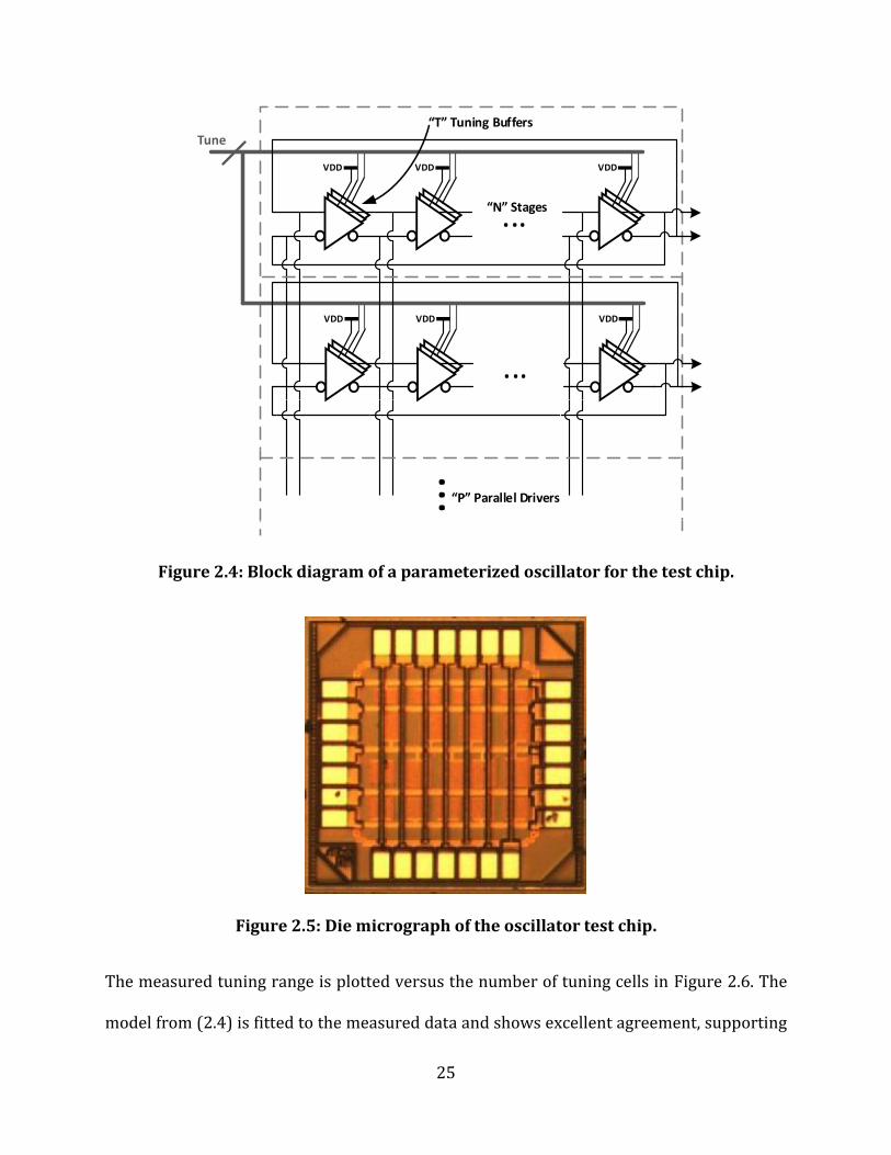
25
Figure 2.4: Block diagram of a parameterized oscillator for the test chip.
Figure 2.5: Die micrograph of the oscillator test chip.
The measured tuning range is plotted versus the number of tuning cells in Figure 2.6. The
model from (2.4) is fitted to the measured data and shows excellent agreement, supporting
Tune
VDD VDD VDD
... N Stages
T Tuning Buffers
VDD VDD VDD
...
... P Parallel Drivers

26
the use of this approach in automating design. In order to further verify the assumptions of
this model, the ratios of 𝐶𝑡𝑢𝑛𝑒/𝐶𝐵 and 𝐼𝑡𝑢𝑛𝑒/𝐼𝐵 were computed using the oscillators with the
maximum and minimum number of tuning cells per stage. Variation of these ratios was found
to be less than 10%; thus, even when making large adjustments to the design using this
simple model, the resulting frequency error is negligible compared to what must already be
designed for to account for PVT variation and mismatch.
Figure 2.6: Tuning range as a function of the number of tuning cells in each stage.
Figure 2.7 shows measurement results from the two methods suggested for reducing phase
noise. Measured phase noise at a 2MHz offset is plotted alongside power and output
frequency. The expected trends for all three measurements are included in the plots. In the
left column, the number of parallel oscillators is adjusted, while in the right column, the
number of stages is increased. In both cases, the deviation from the ideal predicted
improvement is small, supporting both of those techniques as straightforward ways to adjust
the performance of an automatically designed ring oscillator. At a high number of cells, the
importance of good routing becomes more pronounced, as can be seen by the drift away from
the prediction, and thus attention to this aspect is warranted.

27
Figure 2.7: Measurement results showing impact of oscillator parameters of various
performance metrics.
Figure 2.8 shows the three jitter relationships discussed above, along with the relevant
models from (2.17)-(2.19). The dependence of jitter on tuning code is successfully modeled,
while the plots vs. the number of stages and number of parallel oscillators confirm the phase
noise results.

28
Figure 2.8: Jitter models vs. experimental results

29
2.3. Static Timing Analysis for Ring Oscillators
While analytical models can provide a start to a design, they are not sufficient to complete
a design in modern CMOS. Traditionally, SPICE simulations have been used to verify analog
designs; however, they can be very time consuming, preventing fast design iterations. This
section instead presents for the first time a methodology for performing static timing
analysis (STA) on a variety of ring oscillators to accurately simulate the frequency and tuning
range, including the impact of layout, without using SPICE simulations. This is an attractive
alternative to simulation because it dramatically reduces the simulation time of the
oscillator, as well as the cost of the simulation tool. By leveraging the capabilities which
already exist with digital implementation tools, STA for ring oscillators allows an entire
ADPLL to be implemented, optimized, and verified without manual intervention. Along with
jitter and power consumption, output frequency is one of the primary specifications for an
oscillator. Therefore, frequency must be carefully considered throughout the entire design
process. Traditionally, the design process for an oscillator begins with analytical equations
for frequency to generate an initial design, and follows with repeated SPICE simulations to
verify and refine the design. Once parasitic effects are extracted from the physical design,
further iterations with SPICE are used to ensure that performance requirements are satisfied
across all design corners. Due to process scaling, however, this conventional approach to
oscillator design has become more and more inadequate, especially during final verification
when mixed-signal co-simulations are required between the analog and digital circuits. In
this section, we examine the effects which contribute to the difficulty of oscillator design in
advanced nodes, and observe how static timing analysis combined with cell-based ring
oscillators can overcome these difficulties.
30
2.3.1. Circuit Factors Impacting Oscillator Frequency
Traditional methods for estimating ring oscillator frequency without the use of transistor
level simulations have relied on analytical equations. The most basic equation for the
frequency of a ring oscillator is given by:
𝒇𝟎 =
𝟏
𝟐𝑵𝒔𝒕𝒈𝝉𝒅 (2.20)
where 𝑁𝑠𝑡𝑔 is the number of stages and 𝜏𝑑 is the propagation delay for each stage of the ring
oscillator [56].
This expression estimates the oscillator period as the delay for an edge to propagate through
each delay stage twice, which provides the full 360° phase shift needed to sustain oscillation.
This equation captures the fundamental idea behind a ring oscillator, but omits any basis for
determining 𝜏𝑑 , which is made difficult due to the impact of both nonlinearities and parasitic
impedances on oscillator performance.
The most well-known approach for obtaining an analytical equation for 𝜏𝑑 models an
oscillator stage as a constant current source driving a capacitive load, which yields the
following result
𝒇𝟎 =
𝑰𝑺𝑺𝟐𝑵𝒔𝒕𝒈𝑪𝒔𝒕𝒈𝑽𝑺𝑾
(2.21)
Unfortunately, this equation can only be usefully applied to oscillator stages using a constant
bias current, and very inaccurate results can be obtained when using devices from advanced
nodes.
Various approaches towards finding the oscillation frequency using more rigorous analytical
modeling have been proposed, such as in [57], which offers an analysis of differential ring
oscillators with tail current sources, or [56], which examines a single-ended resistor-loaded

31
oscillator. These modelling approaches offer some design insight, but fail in advanced nodes
thanks to second-order effects and parasitics.
Because of these limitations, SPICE simulations have typically been relied upon earlier in the
design cycle. However, oscillation frequencies simulated before parasitic extraction may
differ by more than 2x from final values. This requires overdesign and additional design
cycles after layout in order to meet all specifications across PVT corners, requiring
substantial design resources. A design approach which accounts for the above factors, but
does not entail the overhead of large numbers of repeated circuit simulations across corners
is desirable. To solve this problem, we turn to cell-based digitally-controlled ring oscillators
designed using static-timing analysis.
2.3.2. Cell-Based Digitally-Controlled Oscillators
Cell-based ring oscillators with digital frequency control, as used in [1,2,3] were originally
proposed as a method to avoid the challenges of physical design for analog circuits in
advanced nodes, while also offering easy integration into ADPLLs. However, cell-based
digitally-controlled oscillators (DCOs) also offer advantages from the perspective of
frequency analysis, beginning with the early design stage. As demonstrated above, in order
to account for all factors impacting oscillator frequency in advanced nodes, an increasing
number of circuit parameters must be included. This becomes extremely cumbersome to
accomplish using analytical expressions, especially given the fact that the result may not
agree with simulation. Because cell-based oscillators are built with pre-characterized cells,
better approaches can be used for design and verification.
32
A cell-based oscillator architecture was previously shown in Figure 2.1. Each stage consists
of several identical tristate inverters in parallel. Note that some of inverters may be always
enabled to establish a base frequency; however, they are not treated separately in our
analysis. Using current-source-based models, a characterized cell is essentially represented
as a time and voltage dependent current source, as well as with a time and voltage dependent
capacitance [58]. Unlike analytical equations which attempt to manually identify circuit
parameters which characterize frequency, the current-based models directly capture the
transition behavior while eliminating the need to solve the transistor equations after
characterization is complete. Also, the fact that the model uses a current source means that
examining cells in parallel poses no issues. If the cells are properly characterized, the error
can be within 2% of SPICE simulations [7,8].
Starting with pre-characterized cells, a designer can construct an oscillator by selecting
appropriate cells and combining them into whatever configuration is desired. Let us label
the input capacitance and output current provided by the current-based cell model as 𝐶𝑐𝑒𝑙𝑙
and 𝐼𝑐𝑒𝑙𝑙, respectively. An assembled oscillator will have roughly constant capacitance across
tuning codes compared to the wide changes in transition rates, 𝐼𝑐𝑒𝑙𝑙 and 𝐶𝑐𝑒𝑙𝑙 will be analyzed,
only with respect to transition time. If a single oscillator stage consists of 𝑀𝑠𝑡𝑔 cells, of which
𝑚𝑠𝑡𝑔 are enabled, then the capacitance and current values of each cell are effectively
multiplied by those values. The delay of a stage for a given input transition can then be
calculated:
𝒅(𝝉𝒕𝒓𝒂𝒏) =
𝑴𝒔𝒕𝒈𝑪𝒄𝒆𝒍𝒍(𝝉𝒕𝒓𝒂𝒏)
𝒌𝒎𝒔𝒕𝒈𝑰𝒄𝒆𝒍𝒍(𝝉𝒕𝒓𝒂𝒏) (2.22)

33
where 𝜏𝑡𝑟𝑎𝑛 is the input transition time and 𝑘 is a constant which encompasses the many
effects shown in previous analytical equations, but remains roughly constant for a given
architecture. Then, given an 𝑁 stage oscillator, we can sum and invert the stage delays to find
the oscillator frequency:
𝒇𝟎 =
𝒌𝒎𝑫𝑪𝑶𝑰𝒄𝒆𝒍𝒍(𝝉𝒕𝒓𝒂𝒏)
𝑵𝒔𝒕𝒈𝑴𝑫𝑪𝑶𝑪𝒄𝒆𝒍𝒍(𝝉𝒕𝒓𝒂𝒏) (2.23)
where 𝑚𝐷𝐶𝑂 is the total number of enabled cells, and 𝑀𝐷𝐶𝑂 is the total number of cells.
Looking at this expression further, we can determine the tuning range of a cell-based
oscillator by looking at the characterization of a single cell. When all the cells in the oscillator
are enabled, the frequency is proportional to 𝐼𝑐𝑒𝑙𝑙/𝑁𝑠𝑡𝑔𝐶𝑐𝑒𝑙𝑙, which means that the maximum
frequency of an oscillator depends on the characterized cell and number of stages, regardless
of the number of cells used in parallel. Looking at the case of the minimum frequency, where
only one cell is enabled in each stage, delay per stage can be solved directly from the
characterization data. These estimates based on the characterization data can provide much
better estimates than the analytical expression in the previous section, and are easily able to
be found as part of the STA-based flow.
Cell-based oscillators provide additional design advantages. Once the frequency is known, it
can be combined with individual cell characterization data in order to quickly calculate
power and jitter. Existing digital tools are fully capable of producing power estimates from
such data. Meanwhile, for a given number of stages, jitter and quantization noise both scale
inversely with the number of parallel cells, making it easily predictable.

34
After initial design estimates, it is necessary to fully analyze the DCO across corners, and
make design adjustments to meet specifications. For this purpose, we turn to a full static
timing analysis.
2.4. Proposed Static Timing Analysis Methodology
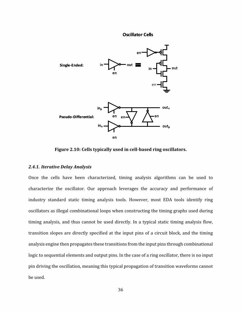
The proposed methodology for using static timing analysis to characterize ring oscillators is
presented in Figure 2.9. Before the timing analysis can be performed on any ring oscillator,
its stages must be described as cells and characterized to produce a timing library. For the
digitally controlled oscillators, the individual cells are typically constructed as tristate
buffers, which are then connected in parallel to construct an oscillator stage. In the case of
pseudo-differential oscillators, a switchable pseudo-differential cell could be used. Both
types of cells are shown in Figure 2.10. Characterization is performed by running SPICE
simulations on individual cells using a variety of input slope and output loading conditions,
and fitting the result to a current source-based model [58]. These oscillator cells should be
characterized over the range of input slews and output loads which is representative of the
conditions which may be seen in the final oscillator design. This range may be wider than the
typical standard cell characterization range, because of the variety of loading scenarios
which occur for different oscillator configurations, but is necessary for accuracy.

35
Cell Characterization
Oscillator Assembly
DCO Code Configuration
Stage-by-Stage Analysis
Sum Stage Delays
Input and Output Transitions Match?
All Relevant DCO Codes Measured?
Final Frequency Tuning Curves
YES
YES
NO
NO
Overall Algorithm
Figure 2.9: Procedure for static timing analysis in ring oscillators.
36
Single-Ended:
Oscillator Cells
Pseudo-Differential:
en
enin out
inp
inn
outn
outp
enen
en
en
in out
en
enin out
inp
inn
outn
outp
enen
en
en
in outSingle-Ended:
Oscillator Cells
Pseudo-Differential:
en
enin out
inp
inn
outn
outp
enen
en
en
in out
en
Figure 2.10: Cells typically used in cell-based ring oscillators.
2.4.1. Iterative Delay Analysis
Once the cells have been characterized, timing analysis algorithms can be used to
characterize the oscillator. Our approach leverages the accuracy and performance of
industry standard static timing analysis tools. However, most EDA tools identify ring
oscillators as illegal combinational loops when constructing the timing graphs used during
timing analysis, and thus cannot be used directly. In a typical static timing analysis flow,
transition slopes are directly specified at the input pins of a circuit block, and the timing
analysis engine then propagates these transitions from the input pins through combinational
logic to sequential elements and output pins. In the case of a ring oscillator, there is no input
pin driving the oscillation, meaning this typical propagation of transition waveforms cannot
be used.

37
One way to overcome the issue of combinational loops is to simply break the oscillator at one
point within the loop and treat the structure as a delay line, driven by some gate. However,
this introduces error sources to the analysis. First, the interconnect parasitics at the point
where the oscillator is broken become inaccurate. Even if this is accounted for, the input
transition waveform is unspecified. It must be selected before timing analysis without
information of what its value should be, propagating an error through the entire delay line.
Instead, an iterative, convergent process must be used to determine the actual transition
waveform at the oscillator. An example of this sort of iterative analysis taken from the
domain of SPICE simulation is the periodic steady state (PSS) analysis as used for oscillators.
In PSS analysis for oscillators, the oscillator state and assumed period are iterated upon until
the analysis confirms periodicity within a specified tolerance [59].
A second issue is the sheer number of paths through an oscillator made of parallel drivers.
In static timing analysis, a timing path consists of delays from gate inputs to gate outputs as
well as delays from routing parasitics. If an oscillator consists of 𝑁 stages with 𝑀 parallel
drivers in each stage, then each individual stage has a total of 𝑀2 timing paths from its input
pins to the input pins of the next stage, since there is a path through each parallel driver in
one stage to each parallel driver in the next stage. This logic can be extended to determine
the total paths from one net in the DCO, through the entire oscillator, and back to the same
net. Thus, if the entire oscillator path were to be timed at once, the total number of paths
would be 𝑀𝑁 for single ended oscillators and 2𝑀𝑁 paths for the differential case. In a
practical case of a placed-and-routed DCO, the number of parallel buffers per stage may climb
as high as 400 in a 5-stage oscillator, which would produce >10 trillion timing paths, which
becomes an intractable computing problem. To solve this issue, the delays and transitions of

38
the oscillator must be evaluated on a stage by stage basis, calculating the 𝑀2 single stage
delay paths at each stage. This reduces the number of paths to 𝑁 ∙ 𝑀2 without eliminating
any paths altogether. The number of paths to evaluate in the previous example would then
be reduced from >10T to a much more manageable 800,000, an improvement of over 1
million times.
In the proposed method, similar to in PSS, an iterative process is used to find the delay
through the entire oscillator. First, the loop is broken and the timing engine is applied to each
stage sequentially, as shown in Figure 2.11. The output of the driving stage is set to have an
ideal transition with an estimated transition slope, which drives the stage of interest. Rise
and fall transitions can be handled simultaneously. Delay is measured through each parallel
cell in the stage of interest, including the extracted interconnect path from the stage of
interest to the following stage, using the standard timing engine. The measured delays
through all cells in the stage, including the delay through the interconnect networks, are then
averaged to produce a single delay number. Additionally, the transitions at the outputs of the
interconnect RC network are averaged to produce new transition values for the rise and fall
times.

39
Figure 2.11: Illustration of static timing analysis procedure for a single stage of the
oscillator.
After a single stage is measured, the calculated transition values are then used to perform
the same calculation on the stage immediately following it. Proceeding around the loop,
transition values are produced for the output of each stage. Once the first stage is reached
again, the difference between the first and second estimates of rise and fall time are
calculated and stored. At this point timing analysis begins a second iteration, and continues
estimating delays and transition slopes around the loop until the error between the current
and previous estimates for each stage are within a specified tolerance. The tolerance can be
specified depending on the accuracy to which calculations are desired. This process can be
applied either after routing with accurate parasitics, or before routing with estimated
preroute parasitics. To further reduce runtime, this analysis can be run with a representative
sample of paths rather than using all paths, at the tradeoff of accuracy.
Disabled Timing Arc
Stage-by-Stage Timing
Driving Stage
Measured Stage
Load Stage
Set Transition Waveform

40
2.4.2. Oscillator Tuning
DCOs feature a digital control input, where a DCO tuning code can be applied to alter the
output frequency. In the case of a DCO, it is necessary to measure the frequency in
configurations other than when all buffers are enabled in the max frequency configuration.
However, while static timing analysis tools can consider possible logic values when
evaluating timing constraints, they are not designed to analyze the effects of
enabling/disabling different numbers of parallel cells. Simply removing buffer cells will not
produce valid frequency results, because the load capacitance of those cells is removed. To
see how this effect could still be addressed, we examine the relationship between the
number of enabled cells in a stage, and the effective load seen by one cell in that stage, as
shown in Figure 2.12.
0
0
1
1
M Parallel Buffers
Figure 2.12: Analysis of oscillator stage load on a cell-by-cell basis. When on m
drivers out of M are enabled, the load is effectively multiplied.

41
In an oscillator stage with 𝑀 drive cells in parallel, and 𝑚 cells enabled, each cell effectively
drives 1/𝑚 of the load. Following this, in the case where all 𝑀 cells are enabled, each cell
drives 1/𝑀 of the load. Thus, the ratio 𝑀/𝑚 describes the difference in load per-cell between
the all-enabled case and the 𝑚-enabled case. Following this logic in order to run timing
analysis at lower tuning codes, the timing analysis setup is configured so that each drive cell
has its effective load increased by 𝑀/𝑚. This yields valid frequency results for the
corresponding DCO tuning code. Once the frequency for each DCO configuration is
calculated, tuning range and resolution are easily determined, as well potential tuning
nonlinearity caused by differences in layout between stages.
2.5. Static Timing Analysis Experimental Results
To verify the methodology, comparisons with SPICE simulations were performed. Two test
designs were used, one single-ended oscillator constructed out of tristate inverter cells and
one pseudo-differential oscillator constructed from the pseudo-differential cell in Figure
2.10. The configurations of the designs are shown in Figure 2.13. Test case 1 is pseudo-
differential, while test case 2 is single-ended. Both are 7-stage oscillators measured after
layout and parasitic extraction. Comparisons were conducted across a number of process
corners. The tested corners are listed in Table 2.1.

42
Figure 2.13: Oscillator configurations used for testing.
Table 2.1: Design Corners Tested
Process Supply Temperature Interconnect
FF 0.99 V -40°C rc-best
FF 0.99 V 125°C rc-best
TT 0.9 V 25°C typical
SS 0.81 V -40°C rc-worst
SS 0.81 V 125°C rc-worst
Figure 2.14a shows a comparison of the oscillator frequency measured by both methods
versus the tuning code for test case 1. The static timing analysis exhibits a consistent
agreement with the simulated data. Figure 2.14b shows the frequency error for the same
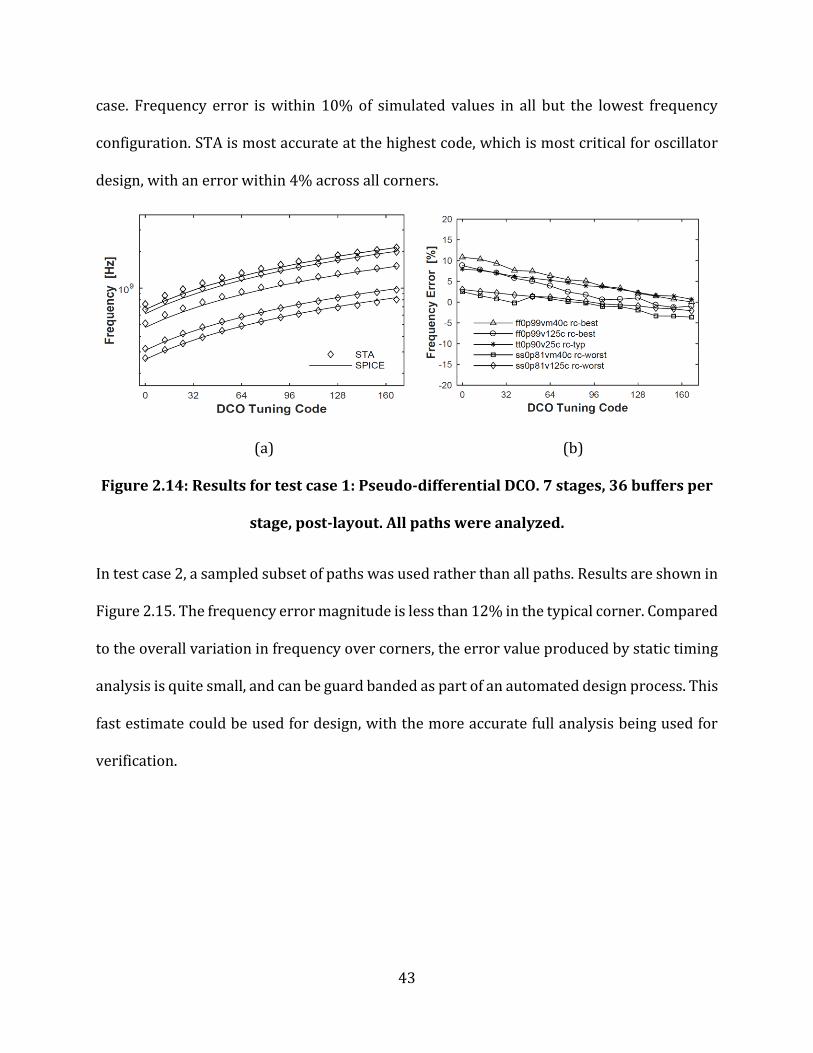
43
case. Frequency error is within 10% of simulated values in all but the lowest frequency
configuration. STA is most accurate at the highest code, which is most critical for oscillator
design, with an error within 4% across all corners.
(a) (b)
Figure 2.14: Results for test case 1: Pseudo-differential DCO. 7 stages, 36 buffers per
stage, post-layout. All paths were analyzed.
In test case 2, a sampled subset of paths was used rather than all paths. Results are shown in
Figure 2.15. The frequency error magnitude is less than 12% in the typical corner. Compared
to the overall variation in frequency over corners, the error value produced by static timing
analysis is quite small, and can be guard banded as part of an automated design process. This
fast estimate could be used for design, with the more accurate full analysis being used for
verification.

44
(a) (b)
Figure 2.15: Results for test case 2: Singled-ended DCO. 7 stages, 36 buffers per stage,
post-layout. A sample of paths was analyzed.
Table 2.2 summarizes error results for both test cases. It also shows the amount of
computation time taken to measure the oscillators using the proposed method, compared to
SPICE simulations. The proposed method offers a speedup of more than 20x in post-layout
frequency measurement.
Table 2.2: Results Summary
Test case 1 Test case 2
Design 7x36 Pseudo-Diff. 7x36 Single-Ended
Design Stage Post-layout Post-layout
STA Method All Paths Sampled Paths
RMS Error 4.24% 9.57%
Max Error 10.75% -19.6%
STA time* 104.4s 29.5s
SPICE time* 522.0s 593.8s
Speedup 5.0x 20.1x
An additional result produced by this analysis provides a means for further design
optimization. Because every path between oscillator stages is measured, the standard
deviation of the delay along paths can be computed. A plotted example of this versus the

45
selected tuning code is shown in Figure 2.16. This statistic is representative of the overall
level of layout mismatch in the placed-and-routed oscillator. Additionally, this information
can be examined on a stage-by-stage basis, or even by comparing individual cells to the mean,
providing information on whether certain areas need more optimization.
(b)
Figure 2.16: Measured standard deviation in oscillator path timings for test case 2.
2.6. Conclusion
We have presented a method for applying existing static timing analysis engines to ring
oscillators, especially those implemented using digital place and route flows. By applying the
timing engine to individual oscillator stages and iterating to achieve convergence, accurate
frequency estimation which agrees with SPICE simulations can be achieved. Additionally, by
altering the load which must be driven by a single oscillator cell, this frequency analysis can
be extended to different tuning codes of DCOs, producing tuning range and resolution data.

46
In addition to time savings, this method of analysis presents a host of other opportunities for
design automation. Because it takes place inside the digital place-and-route flow, adherence
to specifications can be checked before and after routing, and automated adjustments can be
made to improve placement and routing. Several iterations of this can occur without
designer intervention, until specifications are met. By comparison, existing custom design
methods require manual editing of layout, re-running parasitic extraction, and re-simulating
in order to correct performance after layout is completed. The shortened feedback loop
reduces the process of finalizing oscillator layout from weeks to hours.
Finally, integration with the digital design flow opens many possibilities for future
advancement in tool capabilities. The variety of verification steps which are commonly
applied to digital circuits can now be applied to digitally controlled oscillators as well. This
will reduce the uncertainty of inserting an analog block characterized in one environment
into a different digital verification environment. Considering this line of further
development, the proposed technique has the potential to accelerate design of ADPLLs in
advanced nodes.

47
All-Digital Phase-locked loops (ADPLLs) are widely used as clock generators in advanced
digital systems, eliminating several of the downsides of traditional PLLs. However,
traditional ADPLLs still require large amounts of custom layout in the oscillator, which
becomes difficult in advanced process nodes due to exponentially increasing numbers of
design rules. Previous work has demonstrated that integer-N ADPLLs can be implemented
using digital synthesis and automatic place-and-route (APR) tools, resulting in a simplified
and easily customizable design flow [42], [44], [60], [61]. However, meeting specifications
for many modern frequency generation applications requires fractional-N PLLs in order to
achieve the desired tuning resolution, lock time, and in-band phase noise. Additionally, high-
frequency dividers commonly employed in PLLs are major power consumers and introduce
additional jitter into the system. Dividerless PLLs have advantages over conventional
architectures, but traditionally have only been feasible for integer-N PLLs, with one notable
exception where the reference edge is modulated [62]. This chapter presents a dividerless
fractional-N ADPLL synthesized with a digital place and route flow.
3.1. Proposed Architecture
The block diagram of the clock generator is shown in Figure 3.1. Two cascaded PLLs allow
for smaller frequency multiplications, ensuring that locking can occur without the use of a
CHAPTER 3
A Fast-Locking Cascaded PLL using Binary Search

48
divider or frequency locked loop, and providing finer granularity in fractional frequency
selection. Cascading PLLs also has the benefit of pushing spurs further from the center
frequency, as described in [63]. The first PLL (PLL A) uses a 25MHz reference to produce an
output at 160-210MHz. The second PLL (PLL B) takes the output of the first as its reference,
producing the 900MHz output tone. Each PLL uses an identical controller, differing only in
the bit width of the DCO control signals. Because there is no need for a divider or any other
block to operate at the frequency of the output oscillator, no custom design is required to
account for frequencies which may be outside the range of some standard cell libraries.
Frac-N
PLL A
Frac-N
PLL Bref
(25MHz)180MHz 900MHz
fin
fout
Fractional-N
ControllerDLF
Embedded TDC
Binary Search
Engine
Internal Architecture(Duplicated)
Phases
Figure 3.1: Block Diagram of the Proposed Clock Generator
Each DCO is configured such that only one integer multiple of the reference frequency
(25MHz and 160-210MHz for PLLs A and B) is within the tuning range. The use of an
embedded TDC [55] produces a sub-sampled version of the phase error. By computing the
slope of the aliased phase signal, ϕε, the deviation of the DCO oscillation frequency from
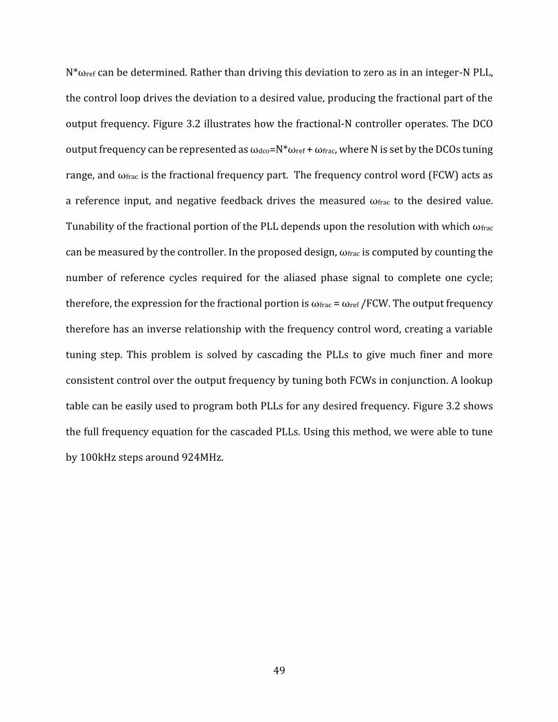
49
N*ωref can be determined. Rather than driving this deviation to zero as in an integer-N PLL,
the control loop drives the deviation to a desired value, producing the fractional part of the
output frequency. Figure 3.2 illustrates how the fractional-N controller operates. The DCO
output frequency can be represented as ωdco=N*ωref + ωfrac, where N is set by the DCOs tuning
range, and ωfrac is the fractional frequency part. The frequency control word (FCW) acts as
a reference input, and negative feedback drives the measured ωfrac to the desired value.
Tunability of the fractional portion of the PLL depends upon the resolution with which ωfrac
can be measured by the controller. In the proposed design, ωfrac is computed by counting the
number of reference cycles required for the aliased phase signal to complete one cycle;
therefore, the expression for the fractional portion is ωfrac = ωref /FCW. The output frequency
therefore has an inverse relationship with the frequency control word, creating a variable
tuning step. This problem is solved by cascading the PLLs to give much finer and more
consistent control over the output frequency by tuning both FCWs in conjunction. A lookup
table can be easily used to program both PLLs for any desired frequency. Figure 3.2 shows
the full frequency equation for the cascaded PLLs. Using this method, we were able to tune
by 100kHz steps around 924MHz.

50
Figure 3.2: Principles of the dividerless fractional-N controller.
The DCOs in both PLLs are shown in Figure 3.3. Both oscillators feature a pseudo-differential
drive cell, which provides improved power supply rejection and provides balanced outputs.
Because the embedded TDC resolution depends on the number of stages in the oscillator, it
is desirable to use as many stages as possible. To this end, the low frequency DCO has 32
stages, while the high frequency DCO has 10 stages. Tuning in the oscillators is accomplished
by two different methods. In the slower oscillator, tuning is accomplished by enabling or
disabling differential tri-state buffers placed in parallel with the main drivers. A novel
capacitance tuning cell was used in order to achieve fine frequency resolution in the high
frequency oscillator. Using a 1-bit DAC consisting simply of a stack of diode-connected PMOS
and two transmission gates, a MOS capacitor can be switched between two different regions
TDCCycle
Counter
φdco φε
-
+
FCW
To DLF
FCW
Sampled Phase
DCOPhase
CycleCount
Tref
1 2 3 1
ωfrac
FCWA=Frequency Control Word of PLL AFCWB=Frequency Control Word of PLL BM,N = Arbitrary Integer
𝑓𝑜𝑢𝑡 ,𝐵 = 𝑀𝑓𝑜𝑢𝑡 ,𝐴 +𝑓𝑜𝑢𝑡 ,𝐴
𝐹𝐶𝑊𝐵
= 𝑀 𝑁𝑓𝑟𝑒𝑓 +𝑓𝑟𝑒𝑓
𝐹𝐶𝑊𝐴
+ 𝑁𝑓𝑟𝑒𝑓 +𝑓𝑟𝑒𝑓
𝐹𝐶𝑊𝐴
/𝐹𝐶𝑊𝐵
𝑓𝑜𝑢𝑡 ,𝐴 = 𝑁𝑓𝑟𝑒𝑓 +𝑓𝑟𝑒𝑓
𝐹𝐶𝑊𝐴
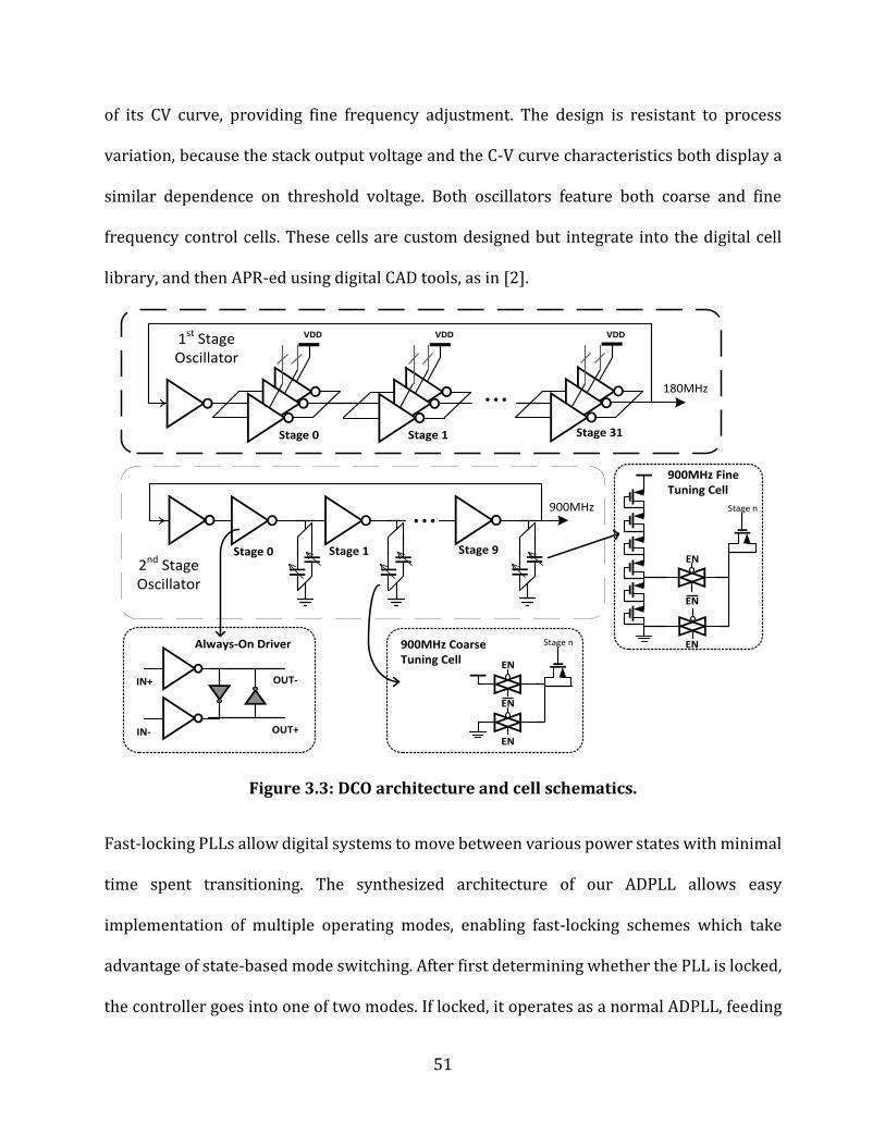
51
of its CV curve, providing fine frequency adjustment. The design is resistant to process
variation, because the stack output voltage and the C-V curve characteristics both display a
similar dependence on threshold voltage. Both oscillators feature both coarse and fine
frequency control cells. These cells are custom designed but integrate into the digital cell
library, and then APR-ed using digital CAD tools, as in [2].
Figure 3.3: DCO architecture and cell schematics.
Fast-locking PLLs allow digital systems to move between various power states with minimal
time spent transitioning. The synthesized architecture of our ADPLL allows easy
implementation of multiple operating modes, enabling fast-locking schemes which take
advantage of state-based mode switching. After first determining whether the PLL is locked,
the controller goes into one of two modes. If locked, it operates as a normal ADPLL, feeding
...Stage 0 Stage 1 Stage 9
900MHz
OUT+IN-
Always-On Driver
OUT-IN+
EN
EN
EN
Stage n
900MHz Fine Tuning Cell
2nd Stage Oscillator
...Stage 0 Stage 1 Stage 31
VDD VDD VDD1st Stage Oscillator
180MHz
EN
EN
EN
Stage n900MHz Coarse Tuning Cell

52
the phase difference signal into the DLF. If not locked, it switches to a fast-locking mode
utilizing a binary search engine to quickly find the desired frequency. The binary search
algorithm leverages full information about the output frequency of the DCO computed in the
controller, a result of the embedded TDC and this fractional-N PLL architecture. When a large
frequency jump is programmed into the PLL, the loop is opened, and the fractional frequency
comparison is instead fed to a binary search controller. By iterating through the coarse
control bits of the DCO, lock time is substantially reduced. Fig. 4 shows the operation of the
binary frequency search, and also shows a measured comparison of lock times. As shown,
the binary search speeds up lock by nearly an order of magnitude.
Figure 3.4: Binary search engine (BSE) behavior and measured lock time results.
3.2. Measurement Results
The ADPLL is fabricated in a 28nm FDSOI CMOS process and occupies 0.09mm2. It consumes
3.0mW, with an RMS jitter of 7.1ps. The measured phase noise spectrum is shown in Figure
3.5. The figure of merit (FOM) is -218.2 dB at a 924MHz output frequency. Performance
characteristics are summarized in Table 3.1 and compared with other synthesized PLLs. The
performance of this clock generator compares favorably with previous synthesized PLLs;
ωout
t
ωFCW
0 0.5 1 1.5 2 2.5 3-80
-70
-60
-50
-40
-30
-20
(a) Binary Frequency Search Behavior
(b) Measured Lock Time
With BSE
Without BSE
Time [ms]
Po
we
r @
ωF
CW
[dB
m]
Start
Locking

53
however, this is the first time a fractional-N PLL has been fully synthesized without using a
divider.
Figure 3.5: Measured phase noise spectrum.
Table 3.1: Performance comparison with state-of-the-art work
This Work RFIC 2013
[2] ISSCC 2013
[4] ISSCC 2014
[3]
FREF (MHz) 25 40.3 25 40-350
FOUT 908-940MHz 403MHz 4-825MHz 0.39-1.41GHz
PN (dBc/Hz) -82 @ 1MHz -98 @ 1MHz -95 @ 1MHz -115@ 1MHz
RMS Jitter 7.1ps 7.9ps 30ps 2.8ps
Area 0.09 mm2 0.1 mm2 0.032 mm2 0.0066 mm2
Power 3.0mW 2.1 mW 3.1mW 0.78mW
FoM* -218.2 dB -218.8 dB -205.5 dB -236.5 dB
VDD 1.1V 1.0V 1.0V 0.8V
Architecture Frac-N ADPLL Int-N ADPLL Frac-N ADPLL Int-N ADPLL
Divider No No Yes Yes
Technology 28 nm 65 nm 28 nm 65 nm
*FoM[dB]=10log10((σt/1s)2x(P/1mW))
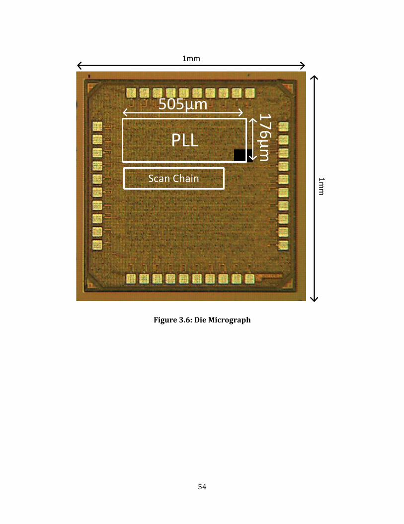
54
Figure 3.6: Die Micrograph
PLL
Scan Chain
505µm 176
µm
1mm
1mm
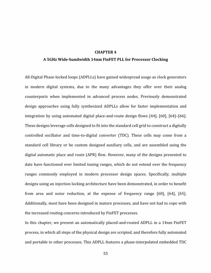
55
All-Digital Phase-locked loops (ADPLLs) have gained widespread usage as clock generators
in modern digital systems, due to the many advantages they offer over their analog
counterparts when implemented in advanced process nodes. Previously demonstrated
design approaches using fully synthesized ADPLLs allow for faster implementation and
integration by using automated digital place-and-route design flows [44], [60], [64]–[66].
These designs leverage cells designed to fit into the standard cell grid to construct a digitally
controlled oscillator and time-to-digital converter (TDC). These cells may come from a
standard cell library or be custom designed auxiliary cells, and are assembled using the
digital automatic place and route (APR) flow. However, many of the designs presented to
date have functioned over limited tuning ranges, which do not extend over the frequency
ranges commonly employed in modern processor design spaces. Specifically, multiple
designs using an injection locking architecture have been demonstrated, in order to benefit
from area and noise reduction, at the expense of frequency range [60], [64], [65].
Additionally, most have been designed in mature processes, and have not had to cope with
the increased routing concerns introduced by FinFET processes.
In this chapter, we present an automatically placed-and-routed ADPLL in a 14nm FinFET
process, in which all steps of the physical design are scripted, and therefore fully automated
and portable to other processes. This ADPLL features a phase-interpolated embedded TDC
CHAPTER 4
A 5GHz Wide-bandwidth 14nm FinFET PLL for Processor Clocking

56
to improve resolution, and is designed to meet the challenges of modern many-core
processor clocking and FinFET DRC requirements. Rather than injection locking, the design
is based around a phase domain architecture [67]. By using optimized auxiliary cells to
construct the DCO, and synthesized resolution enhancing phase interpolator, the proposed
ADPLL achieves the highest output frequency and widest tuning range of any synthesized
PLL to date, and the smallest area for a >1GHz clock generator.
4.1. Synthesizeable ADPLL Design
A conventional phase-domain ADPLL is shown in Figure 4.1. Phase information is measured
using the combination of a counter and a TDC. For each reference cycle, the counter provides
the integer number of DCO cycles which have occurred, while the TDC provides the fractional
number of DCO cycles. The DCO phase measurement is then used in the feedback loop to
drive the oscillator phase to its desired value. However, in this configuration, in-band jitter
performance is limited by TDC resolution and linearity, making it difficult to implement
using APR.
Reference Accumulator
Digital Loop Filter
+
TDC
Counter
+
_FCW fout
DCO
fref
fref
Figure 4.1: Conventional Phase Domain Architecture
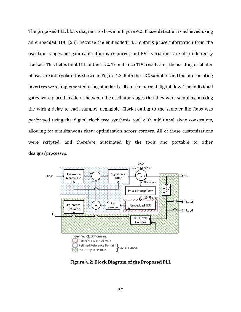
57
The proposed PLL block diagram is shown in Figure 4.2. Phase detection is achieved using
an embedded TDC [55]. Because the embedded TDC obtains phase information from the
oscillator stages, no gain calibration is required, and PVT variations are also inherently
tracked. This helps limit INL in the TDC. To enhance TDC resolution, the existing oscillator
phases are interpolated as shown in Figure 4.3. Both the TDC samplers and the interpolating
inverters were implemented using standard cells in the normal digital flow. The individual
gates were placed inside or between the oscillator stages that they were sampling, making
the wiring delay to each sampler negligible. Clock routing to the sampler flip flops was
performed using the digital clock tree synthesis tool with additional skew constraints,
allowing for simultaneous skew optimization across corners. All of these customizations
were scripted, and therefore automated by the tools and portable to other
designs/processes.
Reference Accumulator
Digital Loop Filter
Reference Retiming
+
Phase Interpolator
Embedded TDC
DCO Cycle Counter
2 /4
+
_FCW
fref
fout
fout /2
fout /4
DCO – GHz
8 Phases
16 Phases
Re-sample
Specified Clock Domains
DCO Output Domain
Retimed Reference Domain
Reference Clock Domain
} Synchronous
Figure 4.2: Block Diagram of the Proposed PLL

58
. . .. . .
fref
Phase 0 Phase 1 Phase 2
Stage Placement Group
Figure 4.3: A Segment of the proposed phase-interpolated embedded TDC
The PLL is designed to operate up to 5GHz, which is twice the desired frequency of 2.5GHz,
so that a divider can be used to provide a clean 50% duty cycle output, required for many
memory circuits. Additionally, the PLL is tunable down to 1GHz and features a wide
bandwidth to enable processor DVFS. Operation at 5GHz places stringent timing
requirements on the feedback counter, so the signal is predivided by 4 before being fed into
the counter. The divide by 2 and divide by 4 signals are then concatenated with the counter
output, recovering the lost edge information, as shown in Figure 4.4. The associated timing
issues arising from having a digital signal with three separate driving clock sources are
identified and handled by the place and route tool. This scheme enables the digital tool to
perform the counter clock routing with relaxed constraints, but still maintain the full counter
resolution. The digital tools account for the skew between original and generated clocks. The
original full speed clock is used for reference retiming, but is made available at the output to
extend the frequency range if the duty cycle requirements of the PLL are not of primary
concern. The retiming circuit is a TDC-based path-selection type, implemented in RTL.
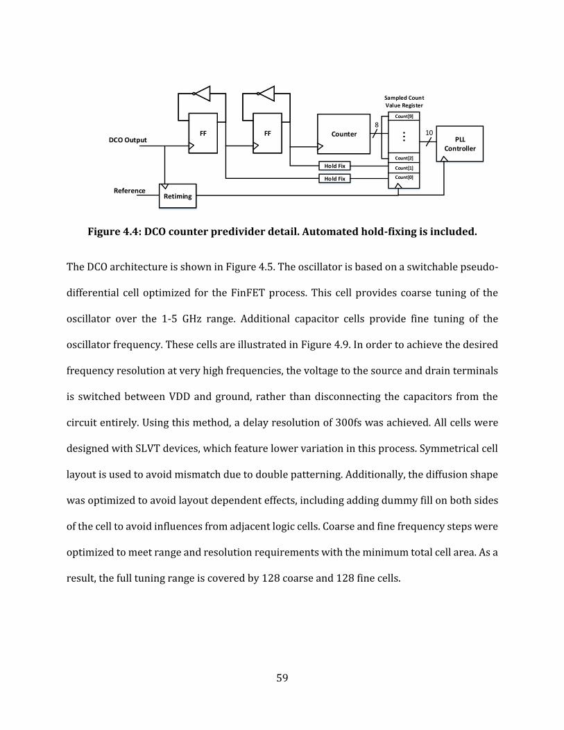
59
CounterCounterFFFFFF FFFFFF
RetimingRetiming
Sampled CountValue Register
Hold Fix
Hold Fix
...
Count[9]
Count[2]
Count[1]
Count[0]
810
PLL Controller
DCO Output
Reference
Figure 4.4: DCO counter predivider detail. Automated hold-fixing is included.
The DCO architecture is shown in Figure 4.5. The oscillator is based on a switchable pseudo-
differential cell optimized for the FinFET process. This cell provides coarse tuning of the
oscillator over the 1-5 GHz range. Additional capacitor cells provide fine tuning of the
oscillator frequency. These cells are illustrated in Figure 4.9. In order to achieve the desired
frequency resolution at very high frequencies, the voltage to the source and drain terminals
is switched between VDD and ground, rather than disconnecting the capacitors from the
circuit entirely. Using this method, a delay resolution of 300fs was achieved. All cells were
designed with SLVT devices, which feature lower variation in this process. Symmetrical cell
layout is used to avoid mismatch due to double patterning. Additionally, the diffusion shape
was optimized to avoid layout dependent effects, including adding dummy fill on both sides
of the cell to avoid influences from adjacent logic cells. Coarse and fine frequency steps were
optimized to meet range and resolution requirements with the minimum total cell area. As a
result, the full tuning range is covered by 128 coarse and 128 fine cells.

60
32x 32x 32x 32x
32x32x32x32x
Figure 4.5: Proposed DCO architecture.
EN
IP
EN
INOPON
VDD
GND
0.576µ
m
1.764µm
EN
IP
EN
INOPON
VDD
GND
0.576µ
m
1.764µm
Coarse Cell
IP IN
EN
VDD
GND
0.576µ
m
0.672µm
Fine Cell
IP IN
EN
VDD
GND
0.576µ
m
0.672µm
Fine Cell
Figure 4.6: Oscillator Auxiliary Cells. Coarse driver cell and fine capacitor cell.
In order to achieve the desired oscillator frequency while taking advantage of the digital
place-and-route flow, additional layout constraints were leveraged in the digital flow. First,
an automated method was used to apply placement guides to each stage of the oscillator,
ensuring that cells from adjacent stages would be placed near each other. Additionally, the
digital router was configured to use wider routing and include additional spacing between
phase signals. These two constraints were fully scripted and automated. This substantially

61
reduced parasitic resistance and capacitance in the oscillator phase routing, enabling the
oscillator to function at the frequencies of interest.
Using an all-digital architecture and leveraging the digital flow also greatly eases
implementation of test features. To leverage this facet of the PLL architecture, an on-chip
test-measurement system was implemented. This system functions like a multi-channel
digital oscilloscope embedded in the controller. It includes a memory, and is able to select
and capture multiplexed digital signals based off of a selectable trigger signal with a
programmable delay. This oscilloscope enables measurement of TDC linearity, lock time, and
in-band phase noise (as measured by the error signal), without external test equipment. This
functionality is highlighted in Figure 4.7.
Reference Accumulator
Digital Loop Filter
Reference Retiming
+
Phase Interpolator
Embedded TDC
DCO Cycle Counter
÷2 /÷4
+
_
fref
fout
fout /2
fout /4
Re-sample
FCW
O-Scope Memory
Scope Trigger
Figure 4.7: Block diagram of on-chip data capture system.

62
4.2. Measurement Results
The ADPLL was constructed in a 14nm FinFET process. The block occupies 0.0195mm2, of
which more than half is used by the integrated oscilloscope. The area of the PLL itself is
0.009mm2. The ADPLL achieves the smallest area among PLLs with >1GHz output. The free-
running DCO consumes 7.6mW from an 0.95V supply, while the controller consumes 2.1mW.
The ADPLL output frequency tunes from 1.0GHz to 5.5GHz across process corners.
TDC nonlinearity was measured using the on-chip measurement system. Measurements of
TDC INL are shown in Figure 4.8. Due to the inherent relationship between the DCO phases
and the TDC value in an embedded TDC, the INL values remain small despite the usage of
automatic place-and-route for physical implementation.
Figure 4.8: Measured TDC nonlinearity.
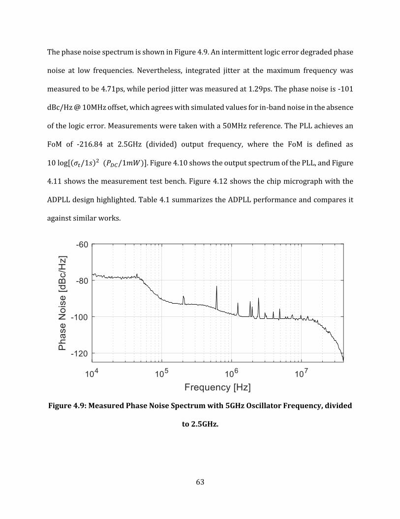
63
The phase noise spectrum is shown in Figure 4.9. An intermittent logic error degraded phase
noise at low frequencies. Nevertheless, integrated jitter at the maximum frequency was
measured to be 4.71ps, while period jitter was measured at 1.29ps. The phase noise is -101
dBc/Hz @ 10MHz offset, which agrees with simulated values for in-band noise in the absence
of the logic error. Measurements were taken with a 50MHz reference. The PLL achieves an
FoM of -216.84 at 2.5GHz (divided) output frequency, where the FoM is defined as
10 log [(𝜎𝑡/1𝑠)2 (𝑃𝐷𝐶/1𝑚𝑊)]. Figure 4.10 shows the output spectrum of the PLL, and Figure
4.11 shows the measurement test bench. Figure 4.12 shows the chip micrograph with the
ADPLL design highlighted. Table 4.1 summarizes the ADPLL performance and compares it
against similar works.
Figure 4.9: Measured Phase Noise Spectrum with 5GHz Oscillator Frequency, divided
to 2.5GHz.
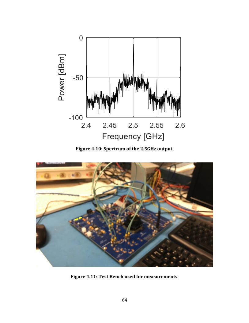
64
Figure 4.10: Spectrum of the 2.5GHz output.
Figure 4.11: Test Bench used for measurements.

65
14
0um
140um
Figure 4.12: Chip Micrograph.
Table 4.1: Performance comparison of ring oscillator ADPLLs
This Work
Deng [64]
Kong [68]
Jang [69]
Yeh [70]
August [71]
Process 14nm 65nm 45nm 28nm SOI 40nm 22nm
Freq. (GHz) 1.0-5.5 0.8-1.7 2.3-2.6 0.8-3.2 3.2 0.3-3.2
Ref. (MHz) 50 50-400 22.6 50 200 40
Power (mW) 9.7 3.0 6.4 [email protected] 2.915 3.4
Area (mm2) 0.009 0.048 0.03 0.049 0.0216 0.2
Period Jitter (ps) 1.29 N/A N/A N/A N/A 0.8
Integ. Jitter (ps) 4.71 3.6 1.68 2.52 3.54 3.1
FoM (dB) -216.8 -224.2 -227.4 -226.5 -224 -224.9
Synthesized? Yes Yes No No No No
Type Int-N Frac-N Frac-N Int-N Int-N Int-N
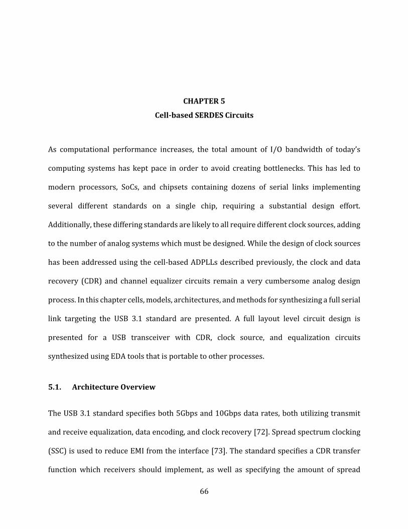
66
As computational performance increases, the total amount of I/O bandwidth of today’s
computing systems has kept pace in order to avoid creating bottlenecks. This has led to
modern processors, SoCs, and chipsets containing dozens of serial links implementing
several different standards on a single chip, requiring a substantial design effort.
Additionally, these differing standards are likely to all require different clock sources, adding
to the number of analog systems which must be designed. While the design of clock sources
has been addressed using the cell-based ADPLLs described previously, the clock and data
recovery (CDR) and channel equalizer circuits remain a very cumbersome analog design
process. In this chapter cells, models, architectures, and methods for synthesizing a full serial
link targeting the USB 3.1 standard are presented. A full layout level circuit design is
presented for a USB transceiver with CDR, clock source, and equalization circuits
synthesized using EDA tools that is portable to other processes.
5.1. Architecture Overview
The USB 3.1 standard specifies both 5Gbps and 10Gbps data rates, both utilizing transmit
and receive equalization, data encoding, and clock recovery [72]. Spread spectrum clocking
(SSC) is used to reduce EMI from the interface [73]. The standard specifies a CDR transfer
function which receivers should implement, as well as specifying the amount of spread
CHAPTER 5
Cell-based SERDES Circuits
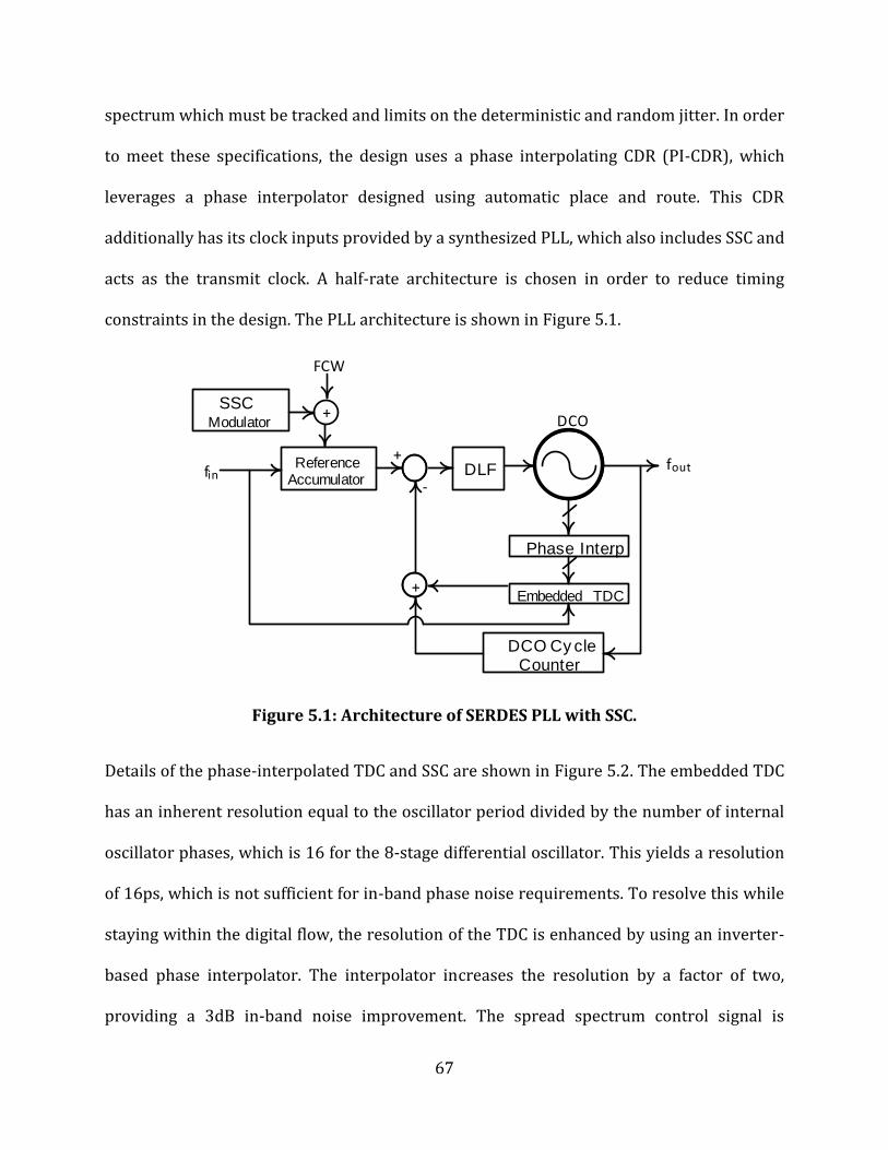
67
spectrum which must be tracked and limits on the deterministic and random jitter. In order
to meet these specifications, the design uses a phase interpolating CDR (PI-CDR), which
leverages a phase interpolator designed using automatic place and route. This CDR
additionally has its clock inputs provided by a synthesized PLL, which also includes SSC and
acts as the transmit clock. A half-rate architecture is chosen in order to reduce timing
constraints in the design. The PLL architecture is shown in Figure 5.1.
Figure 5.1: Architecture of SERDES PLL with SSC.
Details of the phase-interpolated TDC and SSC are shown in Figure 5.2. The embedded TDC
has an inherent resolution equal to the oscillator period divided by the number of internal
oscillator phases, which is 16 for the 8-stage differential oscillator. This yields a resolution
of 16ps, which is not sufficient for in-band phase noise requirements. To resolve this while
staying within the digital flow, the resolution of the TDC is enhanced by using an inverter-
based phase interpolator. The interpolator increases the resolution by a factor of two,
providing a 3dB in-band noise improvement. The spread spectrum control signal is
finfoutReference
AccumulatorDLF
Embedded TDC
-
+
DCO Cy cle Counter
+
FCW
DCO
Phase Interp.
+SSC
Modulator

68
generated using a compact digital triangle generator. A continuous triangle wave
representing 5000ppm of the reference multiplier would require a number of bits far beyond
what is required for quantization noise purposes. This circuit leverages simple addition and
shifting operations to generate a coarsely stepped triangle wave without the need for
complex multiplier hardware being added to the PLL. Instead a combination of step and shift
control values which yield the desired waveform are computed ahead of time and
programmed into the PLL.
Figure 5.2: Detail of (a) phase interpolated embedded TDC and (b) SSC modulator, as
well as (c) SSC modulator output waveform.
DCO Phase [0]
TDC Phase [0]
REF
...
DCO Phase [1]
TDC Phase [1]
TDC Phase [2]
(b)
(a)
SSC Period Spliter
Step Accumulator
Shifter
StepSize
ShiftSize
±1
SSC Period
SSC Modulation Waveform
(c)

69
5.2. CDR Architecture
The CDR uses a half-rate phase-interpolation architecture (PI-CDR), leveraging the fact that
many phases of the oscillator already exist in the frequency generator PLL. The architecture
block diagram is shown in Figure 5.3. A half-rate bang-bang phase detector is used to detect
the phase difference between the currently selected phase and the incoming data stream.
The digital filter includes a rate-reduction of 8x, achieved using a majority voting algorithm,
which reduces high frequency noise from the BBPD as well as further alleviating timing
requirements. The detected phase error is used to adjust which phase of the phase
interpolator is selected to be used as the receiver data clock. The phase interpolator receives
several evenly spaced phases of the half-rate clock as inputs, and produces and output
interpolated between two of these phases. A second order digital filter allows the CDR to
track low frequency phase variations caused by spread spectrum clocking, while still filtering
higher frequency jitter adequately.
Figure 5.3: Architecture of Phase Interpolator-based CDR.

70
5.2.1. Phase Interpolator
An overview of the phase interpolator circuit is shown in Figure 5.4. The PLLs oscillator is
implemented using pseudo-differential cells which results in an even number of phase
outputs. These outputs are broken into even and odd categories and fed into the interpolator.
Based on the desired phase output, the two nearest phases are chosen to interpolate
between. These phases are both fed to 8 multiplexers. By changing the weighting
interpolated phases are both fed to a number of inverters driving the same node. By changing
the weighting code, a number of interpolated phases can be produced.
Figure 5.4: Circuit realization of the synthesizable phase interpolator.
During the interpolation of a rising clock edge, inverters driven by the leading edge switch,
and their NMOS devices begin drawing current from the interpolating node, while PMOS
devices from the trailing edge inverters continue to provide current to the interpolating
node. Consider phase-select values which should generate a code near the trailing edge. If
the input edges to the interpolating inverters are sharp edges, then during the overlap, the
...DCO
odd phases
DCO
even phases
Weighting
Code
Output
Phase
Input
phase select

71
inverters driven by the trailing edge will dominate the inverters from the leading edge,
preventing the output transition from occurring until the trailing edge switches. This results
in significant nonlinearity such as in the top right of Figure 5.5.
Tune[0]
Tune[1]
Tune[15]
...
Vx Vout
Tune[0]
Tune[1]
Tune[15]
...
Vx Vout
Vout
t
Vout
tVout
t
Vout
t
Figure 5.5: Control of PI nonlinearity through input slope tuning.
On the other hand, if the input edges to the phase interpolator are relatively slow, then the
behavior of the interpolating inverters will approach their static transfer function. When the
input transitions overlap and are slow relative to the minimum inverter delay, the ratioed
NMOS and PMOS will perform voltage interpolation between the two edges, which results in
a linear time interpolation. Thus, achieving a linear interpolation requires that the slopes of
the edges to the interpolating inverters are carefully calibrated. This is done through the use
of tunable buffers driving the interpolating inverters, as shown on the left of Figure 5.5.
These tunable buffers are implemented using parallel tristate buffer cells from the standard
cell library. The distribution of the buffer into multiple cells also improves linearity, as the
tuning buffers from various branches are interspersed by the tool, resulting in some amount
of random error averaging.

72
5.3. Physical Implementation of the CDR
In order to successfully complete the CDR design using place and route, and number of
components are needed. After going through the CTLE, the differential data signals must be
converted to single ended signals. Because there are no pre-existing digital cells which
operate on digital data, a custom sampler cell must be created. The schematic of this cell is a
typical dynamic comparator with transmission gate sample-and-hold, as shown in Figure
5.6. This circuit is implemented as a single standard cell, and can easily be characterized
similar to a flip-flop and inserted into the standard cell library. The layout for this
comparator was fit into the standard cell grid. One comparator is used for each edge of the
clock, rising and falling, in order to facilitate the half-rate architecture.
Figure 5.6: Sampling comparator cell.
The phase interpolator is implemented with existing digital cells. Delay based timing
constraints and increased net weighting are applied within the digital implementation tool
in order to ensure successful operation of the interpolation circuitry. To achieve the required
tuning of frequency response, small changes in capacitance can be achieved with existing
CLK
CLK CLK
CLKB CLKB
IP IN
OP
ON
Automatic P&RComparators

73
standard cells, and no custom cells are required. The tuning spans 16 levels in order to meet
the linearity requirements across PVT.
5.4. Receive Equalizer
The receive equalizer is a differential continuous time linear equalizer (CTLE)[74]. A typical
CTLE is illustrated in Figure 5.7. It consists of a differential amplifier with an added zero,
which allows high frequencies to be emphasized, partially correcting the low-pass nature of
the channel. Because this block is inherently an analog amplifier, it is less amenable to a cell-
based approach using a small number of reusable cells. However, it does require digital
tuning, producing many switched elements. These individual elements can be realized as
custom cells, and connected together using the cell-based flow.
Vin+ Vin
-
Vout+-
Figure 5.7: Typical CTLE Receiver.
A cell-based CTLE receiver is shown in Figure 5.8. The original circuit has been split into 4
types of differential cells, with several of each type instantiated to provide tuning of the

74
frequency response. Differential pair, load resistor, tail capacitor, and tail resistor cells were
created through custom design. To reduce offset from mismatch, differential cells were used,
meaning each cell contains a matching element for both the positive and negative sides of
the CTLE. The differential pair, load resistor, and tail capacitor cells are connected in parallel,
while the tail resistor cell is placed in series, and is tuned using a shorting transistor. The
capacitor cell is implemented using a MOS capacitor, while the resistor cells are created using
poly resistors.
Vin+ Vin
-
Vout+-
Load Resistors
Differential Pair
Tail Capacitors
Tail Resis tors
Figure 5.8: Cell-based CTLE circuit, with differential cells.
5.5. Transmit Equalizer
The transmitter features a 3-tap FFE scheme, based off a similar concept to the current DAC
found in [47]. A block diagram is shown in Figure 5.9. First, a half-rate serializer produces a
serial stream of data which is sent through dual-edge triggered flip flops in order to be fed
to the output stage. The output stage consists of three differential cell-based automatically-
placed-and-routed current DACs with outputs shorted together.

75
Serializer
IDAC
IDAC
IDACWei ght[-1]
Wei ght[0]
Wei ght[1]
OUT
2GHzCLK
DATA
Figure 5.9: Transmitter block diagram.
Details of the transmit output stage are shown in Figure 5.10. Each DAC consists of a bank of
differential current steering cells. The current DACs are controlled by the data bit, which
changes the sign of the output current, as well as the FFE tap weights, which are
programmable and control the magnitude of the output current. Separate DACs are used for
the main driver and pre/post-emphasis drivers in order to allow independent strength
adjustment. Because of the relatively high current at the output of the transmitter, special
attention must be paid to the output routing. To accomplish this in the digital flow, the
transmit cells were laid out with pins brought up to a higher metal layer, and custom routing
rules were applied to only the output nets.
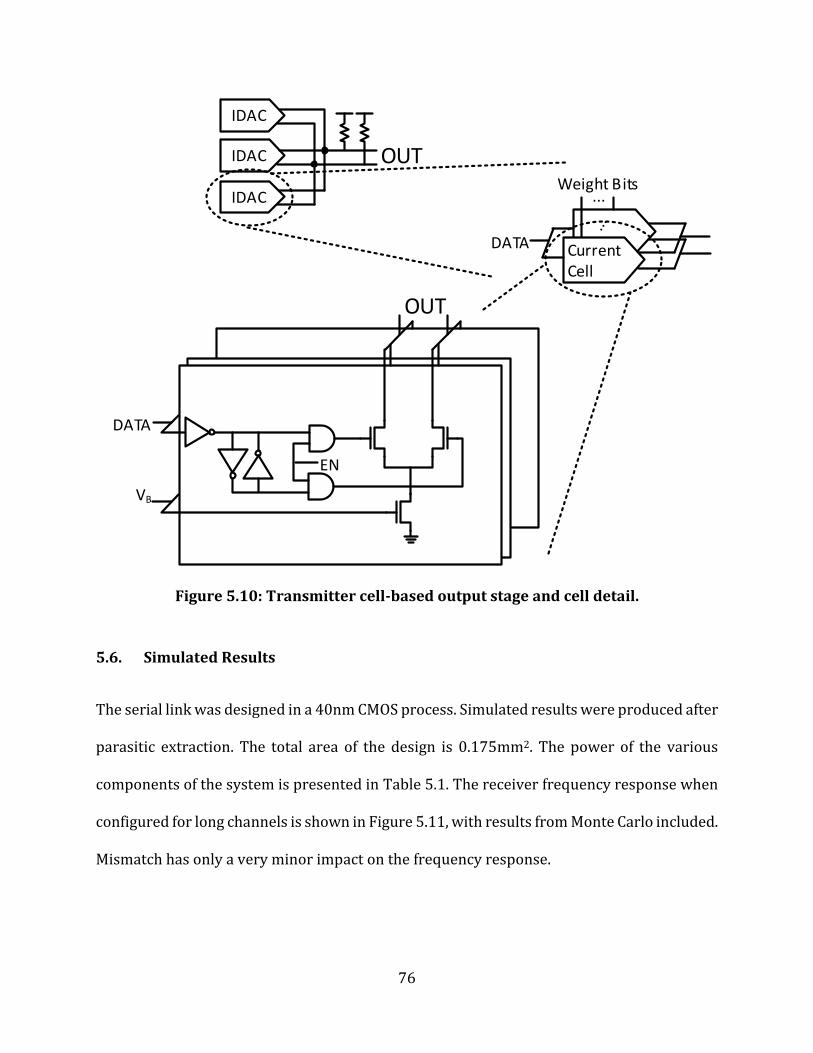
76
Figure 5.10: Transmitter cell-based output stage and cell detail.
5.6. Simulated Results
The serial link was designed in a 40nm CMOS process. Simulated results were produced after
parasitic extraction. The total area of the design is 0.175mm2. The power of the various
components of the system is presented in Table 5.1. The receiver frequency response when
configured for long channels is shown in Figure 5.11, with results from Monte Carlo included.
Mismatch has only a very minor impact on the frequency response.
VB
DATA
EN
OUT
Current Cell
...Weight Bits
DATA
IDAC
IDAC
IDAC
OUT

77
Figure 5.11: Simulated Frequency Response of CTLE Receiver. Monte Carlo Results.
Table 5.1: Power Consumption of System Components
Component Power
Transmitter 2.2mW
Receiver 0.57mW
CDR 6.9 mW
* Phase Interpolator 3.1 mW
PLL 10.3mW
Total 20.0 mW
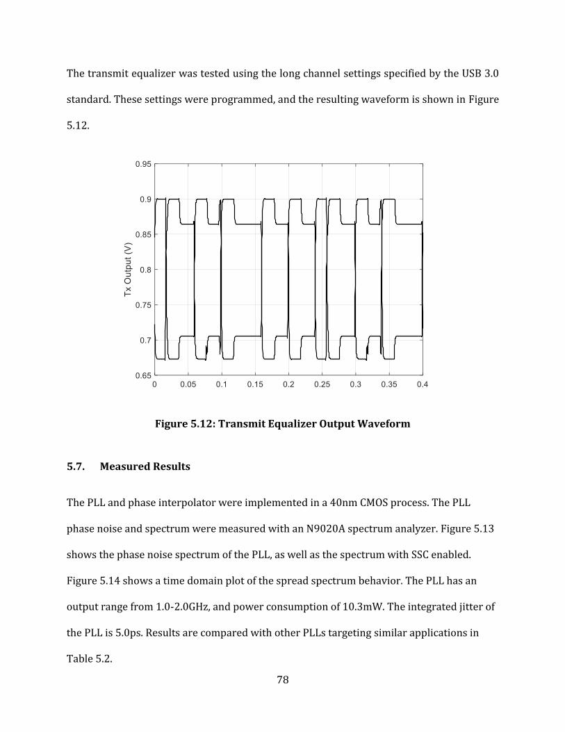
78
The transmit equalizer was tested using the long channel settings specified by the USB 3.0
standard. These settings were programmed, and the resulting waveform is shown in Figure
5.12.
Figure 5.12: Transmit Equalizer Output Waveform
5.7. Measured Results
The PLL and phase interpolator were implemented in a 40nm CMOS process. The PLL
phase noise and spectrum were measured with an N9020A spectrum analyzer. Figure 5.13
shows the phase noise spectrum of the PLL, as well as the spectrum with SSC enabled.
Figure 5.14 shows a time domain plot of the spread spectrum behavior. The PLL has an
output range from 1.0-2.0GHz, and power consumption of 10.3mW. The integrated jitter of
the PLL is 5.0ps. Results are compared with other PLLs targeting similar applications in
Table 5.2.

79
Figure 5.13: PLL Phase Noise and SSC Enabled Spectrum
Figure 5.14: SSC Frequency vs. Time

80
Table 5.2: PLL Performance Comparison
This Work ISSCC ‘15 [64]
ISSCC ‘11 [75]
ISSCC ‘15 [76]
Supply 0.95 V N/A 1.2 V 1.0 Process 40 nm 65 nm 90 nm 40nm SSC Yes No No No Frequency 1-2 GHz 0.8-1.7 GHz 0.25-2 GHz 2.002GHz Osc. Type Ring Ring Ring Ring Integrated Jitter 5.0 ps 3.6 ps 2.3 ps 2.36 ps PLL Power 10.3 mW 3 mW 1.4 mW 9.1 mW
Area(mm2) 0.036 0.0066 N/A 0.046
Synthesized Yes Yes No No
Phase interpolator linearity was measured using a TDS6124C oscilloscope to measure time
intervals between the original and interpolated clocks. Figure 5.15 shows the phase
interpolator linearity after calibration. DNL is < 1LSB across the tuning range, making this
design practical for use in a serial link receiver. The maximum observed DNL is 0.90LSB.
The influence of the 8 input phases on the nonlinearity results is evident. DNL only slightly
exceeds the maximum simulated value without random variation, as shown in Figure 5.15.
This indicates that the random effects are successfully mitigated through the use of parallel
driving cells.
Results from the design are compared with similar designs in Table 5.3. The phase
interpolator operates over a frequency range of 1.5-2.0GHz, and consumes 3.1mW from a
0.95V supply. Compared with the state of the art, this phase interpolator suffers only a
slight linearity penalty, and has a power budget suitable for most CDR applications.
Additionally, it has a small active area allowing for a small CDR implementation. The total
area of gates in the PI is 0.0009mm2, allowing a full CDR to be implemented in 0.010mm2
with a density of 30%. A die photo of the manufactured chip is shown in Figure 5.16.

81
Figure 5.15: Phase Interpolator Nonlinearity
Table 5.3: Phase Interpolator Performance Comparison
This Work JSSC ‘13 [77]
VLSI ‘16 [78]
ISSCC ‘11 [79]
Type Inverter-based
Inverter-based
Current-based
Current-based
Supply 0.95V 1.2V 1.2V 1.2V Process 40 nm 65nm 65nm 65nm Frequency 1.5-2 GHz 0.1-1.5GHz 4-8GHz 1-6GHz Bits 6 8 6 Analog Max INL 2.21 0.99 N/A 6.5° * Max DNL 0.90 0.45 0.48 N/A Power 3.1 mW
@2GHz** 4.3mW @1.5GHz**
87.6mW @16Gbps†
3.8mW @6Gbps†
Area (mm2) 0.0009** 0.0192†
0.060** 0.088† 0.0035†
Synthesized Yes No No No *Equivalent to 1.16 bits in a 6b digital PI ** PI only †with CDR

82
PI-CDR
PLL Cont.
DC
O
1m
m
1mm
10
0µ
m
100µm200µm
15
0µ
m
70µm
90
µm
Figure 5.16: Serial Link Die Photo

83
As analog design has become more and more difficult relative to digital design due to process
scaling, many approaches to analog design automation have been developed. Among them,
cell-based analog design automation is a recent development which leverages digital design
tools and highly digital architectures in order to accelerate analog design. This approach can
also increase design flexibility and reduce area by allowing application specific design
customization in place of heavily reused analog IP blocks. Previous work has demonstrated
the viability of this approach for ADPLLs. However, this work is limited in the range of
specifications and process technologies it targeted, as well as focusing only on physical
design automation while ignoring circuit design automation.
This thesis addresses both of these issues. First, both analytical and numerical modeling
strategies which can be applied to the design of cell-based ring oscillators are presented. The
analytical models allow for prediction of what oscillator configuration can be used to achieve
a given circuit specification, leveraging the cell-based nature of the design and without
detailed knowledge of parasitics. The numerical timing model allows for accelerated
verification and iteration of the design to meet frequency specifications without the use of
SPICE simulations, reducing design times. Both of these models together enable the
development of a fully automated design flow.
CHAPTER 6
Conclusions
84
The usefulness of these automation techniques is limited if they cannot be applied to
advanced process nodes or modern use cases. This thesis presented circuit strategies to
enable fractional-N operation and high output frequencies in cell-based ADPLLs designed in
modern processes. Among the many circuit factors which need to be addressed in these
processes are design for noise, mismatch, and parasitic resistance. Two prototypes were
fabricated: the first in a 28nm FD-SOI process, and the second in a 14nm FinFET process.
These designs demonstrated the applicability of these ADPLLs to modern design challenges.
Finally, this thesis extended the cell-based design methodology to an additional class of
circuits: SERDES interfaces. Cell-based circuit approaches for a CDR, FIR Tx Equalizer, and
CTLE Rx Equalizer were presented. A prototype targeting the USB 3.1 specification was
implemented in a 40nm CMOS process, and represents the first synthesized SERDES. The
first step demonstates the feasibility of implemented these types of circuits using an
automated cell-based approach, removing additional design bottlenecks.
6.1. Future Work
Cell-based implementation of analog blocks has recently begun attracting attention from
industry, which has lent additional clarity to the major advantages of this approach. The
potential for full design automation of these circuits can change how they are utilized at the
system level, potentially making a bigger impact that simply reducing design time. With this
in mind, potential future directions for this work are discussed below.

85
6.1.1. Additional circuit varieties
To date, the cell-based design methodology for analog has been primarily applied to ring
oscillator PLLs and to current steering DACs. This thesis extends the work to a limited subset
of SERDES circuits as well. However, there are still a number of analog blocks commonly
used in modern processors and systems-on-chip which could potentially be implemented
using this approach. Most directly related to the work in this thesis would be a cell-based LC
oscillator, which has been demonstrated to some extent in [49]. Additionally, an LC PLL
would enable additional SERDES standards to be targeted, with additional circuit
requirements. Other circuits of potential interest are voltages regulators and ADCs.
6.1.2. Analog specific EDA support
The purpose of this research is to enable design automation of analog circuits, so it is not
enough to simply consider circuits; the approach to automation is also essential for achieving
useful performance. Chapter 2 of this thesis developed multiple modeling techniques
intended to be used for performance evaluation in a fully automated PLL design flow. Missing
from these models is a numerical approach to evaluating jitter, analogous to the use of static
timing analysis for frequency evaluation. While analytical predictions of jitter a typically
reliable enough to design with guard banding, a cell-based numerical model which correlates
with SPICE could largely remove the need to run SPICE simulations on generated PLLs
altogether. Several other research topics which fall under the umbrella of EDA could
contribute to the usefulness of the cell-based analog design flow. Examples include supply-
sensitivity modeling and specialized placement and routing of oscillator cells.

86
6.1.3. System level usage of automated analog design
Currently, analog system requirements are typically planned early in a chip design cycle, and
are relatively inflexible due to the large custom design effort that goes into creating them.
However, if analog circuits can be quickly generated to fill a specific role, they can potentially
be used in new parts of a system later in the design cycle. For example, additional
synthesized voltage regulators could be inserted into the design late in the design cycle based
on simulated supply noise values, without requiring large floorplan changes imposed by a
hard macro regulator. The value of these sorts of system-wide usages is speculative, but
potentially much higher than simply the benefits of design automation.
87
REFERENCES
[1] C. Gonzalez et al., “POWER9TM: A processor family optimized for cognitive computing
with 25Gb/s accelerator links and 16Gb/s PCIe Gen4,” in 2017 IEEE International
Solid-State Circuits Conference (ISSCC), 2017, pp. 50–51.
[2] B. Bowhill et al., “The Xeon® processor E5-2600 v3: A 22nm 18-core product family,”
in 2015 IEEE International Solid-State Circuits Conference - (ISSCC) Digest of Technical
Papers, 2015, pp. 1–3.
[3] H. Mair et al., “A highly integrated smartphone SoC featuring a 2.5GHz octa-core CPU
with advanced high-performance and low-power techniques,” in 2015 IEEE
International Solid-State Circuits Conference - (ISSCC) Digest of Technical Papers, 2015,
pp. 1–3.
[4] Y. Lee et al., “A Modular 1 mm3 Die-Stacked Sensing Platform With Low Power I2C
Inter-Die Communication and Multi-Modal Energy Harvesting,” IEEE J. Solid-State
Circuits, vol. 48, no. 1, pp. 229–243, Jan. 2013.
[5] Y. Lee et al., “A Modular 1mm 3 Die-Stacked Sensing Platform With Optical
Communication and Multi-Modal Energy Harvesting,” in ISSCC, 2012, pp. 212–213.
[6] G. Desoli et al., “A 2.9TOPS/W deep convolutional neural network SoC in FD-SOI 28nm
for intelligent embedded systems,” in 2017 IEEE International Solid-State Circuits
Conference (ISSCC), 2017, pp. 238–239.
[7] B. Karpinskyy, Y. Lee, Y. Choi, Y. Kim, M. Noh, and S. Lee, “Physically unclonable
function for secure key generation with a key error rate of 2E-38 in 45nm smart-card
chips,” in 2016 IEEE International Solid-State Circuits Conference (ISSCC), 2016, pp.
158–160.
[8] D. Rosso, “Global Semiconductor Sales Reach $339 Billion in 2016,” Semiconductor
Industry Association, 2017. [Online]. Available:
https://www.semiconductors.org/news/2017/02/02/global_sales_report_2015/glo
88
bal_semiconductor_sales_reach_339_billion_in_2016/. [Accessed: 06-Sep-2017].
[9] Yinug Falin, “What End Use Applications Drove Semiconductor Sales in 2014?,” 2015.
[10] N. E. H. Weste and D. M. Harris, CMOS VLSI Design: A Circuits and Systems Perspective,
vol. 53, no. 9. 2013.
[11] W. Krenik, D. D. Buss, and P. Rickert, “Cellular handset integration - SIP versus SOC,”
IEEE J. Solid-State Circuits, vol. 40, no. 9, pp. 1839–1846, Sep. 2005.
[12] “Qualcomm ® Snapdragon TM 600E Processor Device Specification,” 2017.
[13] G. E. Moore, “No exponential is forever: but ‘Forever’ can be delayed! [semiconductor
industry],” in 2003 IEEE International Solid-State Circuits Conference, 2003. Digest of
Technical Papers. ISSCC., vol. 1, pp. 20–23.
[14] G. Martin et al., “An integrated LSI design aids system,” Microelectronics J., vol. 12, no.
4, pp. 18–22, 1981.
[15] P. Kurup and T. Abbasi, Logic Synthesis Using Synopsys®. Boston, MA: Springer US,
1995.
[16] D. E. Thomas, “The automatic synthesis of digital systems,” Proc. IEEE, vol. 69, no. 10,
pp. 1200–1211, 1981.
[17] M. J. M. Pelgrom, A. C. J. Duinmaijer, and A. P. G. Welbers, “Matching Properties of MOS
Transistors,” IEEE J. Solid-State Circuits, vol. 24, no. 5, pp. 1433–1439, Oct. 1989.
[18] R. J. Baker, CMOS: Circuit design, layout, and simulation, 3rd ed. Piscataway, NJ: Wiley,
2010.
[19] P. Nuzzo and A. Sangiovanni-Vincentelli, “Robustness in analog systems: Design
techniques, methodologies and tools,” in 2011 6th IEEE International Symposium on
Industrial and Embedded Systems, 2011, pp. 194–203.
[20] S. Natarajan et al., “A 14nm logic technology featuring 2<sup>nd</sup>-
generation FinFET, air-gapped interconnects, self-aligned double patterning and a
0.0588 &#x00B5;m<sup>2</sup> SRAM cell size,” in 2014 IEEE
International Electron Devices Meeting, 2014, p. 3.7.1-3.7.3.
[21] D. Burnett, S. Parihar, H. Ramamurthy, and S. Balasubramanian, “FinFET SRAM design
challenges,” in 2014 IEEE International Conference on IC Design & Technology, 2014,
pp. 1–4.
[22] J.-M. Brunet, “Reducing The Tapeout Crunch With Signoff Confidence,” Semiconductor

89
Engineering, 2013. [Online]. Available: http://semiengineering.com/reducing-
tapeout-crunch-signoff-confidence/. [Accessed: 28-Aug-2017].
[23] B. Murmann, “Digitally Assisted Analog Circuits,” IEEE Micro, vol. 26, no. 2, pp. 38–47,
Mar. 2006.
[24] M. H. Perrott, “Tutorial on Digital Phase-Locked Loops,” in CICC, 2009.
[25] S. Li et al., “Reconfigurable All-Band RF CMOS Transceiver for
GPS/GLONASS/Galileo/Beidou With Digitally Assisted Calibration,” IEEE Trans. Very
Large Scale Integr. Syst., vol. 23, no. 9, pp. 1814–1827, Sep. 2015.
[26] B. King, J. Xia, and S. Boumaiza, “Digitally-Assisted RF-Analog Self Interference
Cancellation for Wideband Full-Duplex Radios,” IEEE Trans. Circuits Syst. II Express
Briefs, pp. 1–1, 2017.
[27] Chao Lu et al., “A 24.7dBm all-digital RF transmitter for multimode broadband
applications in 40nm CMOS,” in 2013 IEEE International Solid-State Circuits Conference
Digest of Technical Papers, 2013, pp. 332–333.
[28] P. Madoglio, M. Zanuso, S. Levantino, C. Samori, and A. L. Lacaita, “Quantization Effects
in All-Digital Phase-Locked Loops,” IEEE Trans. Circuits Syst. II Express Briefs, vol. 54,
no. 12, pp. 1120–1124, Dec. 2007.
[29] M. A. Massetti et al., “A CMOS-based mixed analog-logic standard cell product family,”
in Proceedings of the IEEE 1988 Custom Integrated Circuits Conference, p. 24.1/1-
24.1/6.
[30] R. J. Bowman, “Introduction to CMOS analog standard cell ASIC design,” in Proceedings.,
Second Annual IEEE ASIC Seminar and Exhibit, pp. T2-1-4.
[31] M. G. R. Degrauwe et al., “IDAC: an interactive design tool for analog CMOS circuits,”
IEEE J. Solid-State Circuits, vol. 22, no. 6, pp. 1106–1116, Dec. 1987.
[32] Koh Han Young, C. H. Sequin, and P. R. Gray, “Automatic layout generation for CMOS
operational amplifiers,” in [1988] IEEE International Conference on Computer-Aided
Design (ICCAD-89) Digest of Technical Papers, pp. 548–551.
[33] R. Harjani, R. A. Rutenbar, and L. R. Carley, “A prototype framework for knowledge-
based analog circuit synthesis,” in 24th ACM/IEEE conference proceedings on Design
automation conference - DAC ’87, 1987, pp. 42–49.
[34] R. Harjani, R. A. Rutenbar, and L. R. Carley, “Analog circuit synthesis and exploration

90
in OASYS,” in Proceedings 1988 IEEE International Conference on Computer Design:
VLSI, pp. 44–47.
[35] Hongzhou Liu, A. Singhee, R. A. Rutenbar, and L. R. Carley, “Remembrance of circuits
past: macromodeling by data mining in large analog design spaces,” in Proceedings
2002 Design Automation Conference (IEEE Cat. No.02CH37324), 2002, pp. 437–442.
[36] R. A. Rutenbar, “Design Automation for Analog: The Next Generation of Tool
Challenges The Mixed-Signal Design Problem Digital Analog,” 2006.
[37] M. Taherzadeh-Sani, R. Lotfi, H. Zare-Hoseini, and O. Shoaei, “Design optimization of
analog integrated circuits using simulation-based genetic algorithm,” in SCS 2003.
International Symposium on Signals, Circuits and Systems. Proceedings (Cat.
No.03EX720), vol. 1, pp. 73–76.
[38] “Cadence acquires analog layout vendor Neolinear,” EE Times, 06-Apr-2004.
[39] “Costello’s analog automation pioneer, Barcelona, to fold,” EE Times, 04-Mar-2005.
[40] “Cadence acquires Antrim assets,” EE Times, 22-Nov-2002.
[41] R. A. Rutenbar, “Analog Synthesis (and Verification) Revisited: What’s Missing?,” in
2012 International Conference on Synthesis, Modeling, Analysis and Simulation Methods
and Applications to Circuit Design (SMACD), 2012.
[42] M. Faisal and D. D. Wentzloff, “An automatically placed-and-routed ADPLL for the
medradio band using PWM to enhance DCO resolution,” Dig. Pap. - IEEE Radio Freq.
Integr. Circuits Symp., pp. 115–118, 2013.
[43] Youngmin Park and D. D. Wentzloff, “An All-Digital 12 pJ/Pulse IR-UWB Transmitter
Synthesized From a Standard Cell Library,” IEEE J. Solid-State Circuits, vol. 46, no. 5,
pp. 1147–1157, May 2011.
[44] Y. Park and D. D. Wentzloff, “An all-digital PLL synthesized from a digital standard cell
library in 65nm CMOS,” Proc. Cust. Integr. Circuits Conf., pp. 1–4, 2011.
[45] Y. Park and D. D. Wentzloff, “A cyclic Vernier time-to-digital converter synthesized
from a 65nm CMOS standard library,” ISCAS 2010 - 2010 IEEE Int. Symp. Circuits Syst.
Nano-Bio Circuit Fabr. Syst., pp. 3561–3564, 2010.
[46] S. Weaver, B. Hershberg, and U. K. Moon, “Digitally synthesized stochastic flash ADC
using only standard digital cells,” IEEE Trans. Circuits Syst. I Regul. Pap., vol. 61, no. 1,
pp. 84–91, 2014.

91
[47] E. Ansari and D. D. Wentzloff, “A 5mW 250MS/s 12-bit synthesized digital to analog
converter,” in Proceedings of the IEEE 2014 Custom Integrated Circuits Conference,
2014, pp. 1–4.
[48] M. Faisal, N. E. Roberts, and D. D. Wentzloff, “A 300nW near-threshold 187.5-500 kHz
programmable clock generator for ultra low power SoCs,” in 2015 IEEE SOI-3D-
Subthreshold Microelectronics Technology Unified Conference (S3S), 2015, pp. 1–3.
[49] D. Yang et al., “An HDL-synthesized injection-locked PLL using LC-based DCO for on-
chip clock generation,” in 2017 22nd Asia and South Pacific Design Automation
Conference (ASP-DAC), 2017, pp. 13–14.
[50] J. Galloway and A. Cole, “Phase-locked loop design through the decades,” Embedded,
2011. [Online]. Available: http://www.embedded.com/design/mcus-processors-and-
socs/4428712/Phase-locked-loop-design-through-the-decades---Part-1. [Accessed:
09-Sep-2017].
[51] J. Galloway and R. Caplan, “Is there a "one-size fits all" SOC PLL?,” Design &
Reuse, 2011. [Online]. Available: https://www.design-reuse.com/articles/25320/pll-
architecture.html. [Accessed: 09-Sep-2017].
[52] D. Yang et al., “An automatic place-and-routed two-stage fractional-N injection-locked
PLL using soft injection,” Proc. Asia South Pacific Des. Autom. Conf. ASP-DAC, vol. 25–
28–Janu, no. 3, pp. 1–2, 2016.
[53] W. Deng et al., “A fully synthesizable all-digital pll with interpolative phase coupled
oscillator, current-output DAC, and fine-resolution digital varactor using gated edge
injection technique,” IEEE J. Solid-State Circuits, vol. 50, no. 1, pp. 68–80, 2015.
[54] A. A. Abidi, “Phase Noise and Jitter in CMOS Ring Oscillators,” IEEE J. Solid-State
Circuits, vol. 41, no. 8, pp. 1803–1816, Aug. 2006.
[55] M. S. W. Chen, D. Su, and S. Mehta, “A calibration-free 800 MHz fractional-N digital PLL
with embedded TDC,” IEEE J. Solid-State Circuits, vol. 45, no. 12, pp. 2819–2827, 2010.
[56] P. M. Farahabadi, H. Miar-Naimi, and a. Ebrahimzadeh, “Closed-Form Analytical
Equations for Amplitude and Frequency of High-Frequency CMOS Ring Oscillators,”
IEEE Trans. Circuits Syst. I Regul. Pap., vol. 56, no. 12, pp. 2669–2677, 2009.
[57] S. Docking and M. Sachdev, “An analytical equation for the oscillation frequency of
high-frequency ring oscillators,” IEEE J. Solid-State Circuits, vol. 39, no. 3, pp. 533–537,

92
2004.
[58] Synopsys, “CCS Timing Technical White Paper,” User Man., pp. 1–15, 2006.
[59] T. Aprille and T. Trick, “A computer algorithm to determine the steady-state response
of nonlinear oscillators,” IEEE Trans. Circuit Theory, vol. 19, no. 4, pp. 354–360, 1972.
[60] W. Deng et al., “A 0.0066mm2 780µW fully synthesizable PLL with a current-output
DAC and an interpolative phase-coupled oscillator using edge-injection technique,”
Dig. Tech. Pap. - IEEE Int. Solid-State Circuits Conf., vol. 57, pp. 266–267, 2014.
[61] Wooseok Kim, Jaejin Park, Jihyun Kim, Taeik Kim, HoJin Park, and DeogKyoon Jeong,
“A 0.032mm2 3.1mW synthesized pixel clock generator with 30psrms integrated jitter
and 10-to-630MHz DCO tuning range,” in 2013 IEEE International Solid-State Circuits
Conference Digest of Technical Papers, 2013, pp. 250–251.
[62] P.-C. Huang, W.-S. Chang, and T.-C. Lee, “21.2 A 2.3GHz fractional-N dividerless phase-
locked loop with −112dBc/Hz in-band phase noise,” in 2014 IEEE International Solid-
State Circuits Conference Digest of Technical Papers (ISSCC), 2014, pp. 362–363.
[63] D. Park and S. Cho, “A 14.2mW 2.55-to-3GHz cascaded PLL with reference injection,
800MHz delta-sigma modulator and 255fsrms integrated jitter in 0.13μm CMOS,” in
2012 IEEE International Solid-State Circuits Conference, 2012, pp. 344–346.
[64] W. Deng et al., “A 0.048mm2 3mW synthesizable fractional-N PLL with a soft injection-
locking technique,” Dig. Tech. Pap. - IEEE Int. Solid-State Circuits Conf., vol. 58, pp. 252–
253, 2015.
[65] W. Deng, A. Musa, T. Siriburanon, M. Miyahara, K. Okada, and A. Matsuzawa, “A
0.022mm2 970??W dual-loop injection-locked PLL with -243dB FOM using
synthesizable all-digital PVT calibration circuits,” in Digest of Technical Papers - IEEE
International Solid-State Circuits Conference, 2013, vol. 56, pp. 248–249.
[66] S. Kim et al., “A 2 GHz Synthesized Fractional-N ADPLL With Dual-Referenced
Interpolating TDC,” IEEE J. Solid-State Circuits, vol. 51, no. 2, pp. 391–400, Feb. 2016.
[67] P. A. P. Loop, R. B. Staszewski, and P. T. Balsara, “Phase-Domain All-Digital Phase-
Locked Loop,” vol. 52, no. 3, pp. 159–163, 2005.
[68] L. Kong and B. Razavi, “A 2.4-GHz 6.4-mW fractional-N inductorless RF synthesizer,”
IEEE Symp. VLSI Circuits, Dig. Tech. Pap., vol. 2016–Septe, pp. 9–10, 2016.
[69] T. Jang, S. Jeong, D. Jeon, K. D. Choo, D. Sylvester, and D. Blaauw, “8.4 A 2.5ps 0.8-to-
93
3.2GHz bang-bang phase- and frequency-detector-based all-digital PLL with noise self-
adjustment,” in 2017 IEEE International Solid-State Circuits Conference (ISSCC), 2017,
pp. 148–149.
[70] C.-W. Yeh, C.-E. Hsieh, and S.-I. Liu, “19.5 A 3.2GHz digital phase-locked loop with
background supply-noise cancellation,” in 2016 IEEE International Solid-State Circuits
Conference (ISSCC), 2016, pp. 332–333.
[71] N. August, H. J. Lee, M. Vandepas, and R. Parker, “A TDC-less ADPLL with 200-to-
3200MHz range and 3mW power dissipation for mobile SoC clocking in 22nm CMOS,”
Dig. Tech. Pap. - IEEE Int. Solid-State Circuits Conf., vol. 55, pp. 246–247, 2012.
[72] “Universal Serial Bus 3.1 Specification,” 2013.
[73] N. Keskin and H. Liu, “Practical considerations for electromagnetic interference
suppression rate with spread spectrum clocking,” IEEE Electromagn. Compat. Mag.,
vol. 5, no. 2, pp. 57–60, 2016.
[74] S. Gondi and B. Razavi, “Equalization and Clock and Data Recovery Techniques for 10-
Gb/s CMOS Serial-Link Receivers,” IEEE J. Solid-State Circuits, vol. 42, no. 9, pp. 1999–
2011, Sep. 2007.
[75] R. Inti et al., “A highly digital 0.5-to-4Gb/s 1.9mW/Gb/s serial-link transceiver using
current-recycling in 90nm CMOS,” Dig. Tech. Pap. - IEEE Int. Solid-State Circuits Conf.,
pp. 152–153, Feb. 2011.
[76] C.-F. F. Liang and P.-Y. Y. Wang, “A wideband fractional-N ring PLL using a near-ground
pre-distorted switched-capacitor loop filter,” Dig. Tech. Pap. - IEEE Int. Solid-State
Circuits Conf., vol. 58, pp. 190–191, Feb. 2015.
[77] M.-S. S. Chen, A. A. Hafez, and C.-K. K. K. K. Yang, “A 0.1-1.5 ghz 8-bit inverter-based
digital-to-phase converter using harmonic rejection,” IEEE J. Solid-State Circuits, vol.
48, no. 11, pp. 2681–2692, Nov. 2013.
[78] G. Wu et al., “A 1–16 Gb/s All-Digital Clock and Data Recovery With a Wideband High-
Linearity Phase Interpolator,” IEEE Trans. Very Large Scale Integr. Syst., vol. 24, no. 7,
pp. 2511–2520, Jul. 2016.
[79] B. Abiri, R. Shivnaraine, A. Sheikholeslami, H. Tamura, and M. Kibune, “A 1-to-6Gb/s
phase-interpolator-based burst-mode CDR in 65nm CMOS,” Dig. Tech. Pap. - IEEE Int.
Solid-State Circuits Conf., pp. 154–155, Feb. 2011.