click max20796 dual-phase scalable integrated voltage
TRANSCRIPT

General Description The MAX20796 offers a fully integrated, highly efficient, two-phase switching regulator for applications operating from 4.5V to 16V and requiring up to 60A maximum load or 90A with an optional third-phase external power stage. The output voltage range can be configured from 0.5V to 5.5V with some restrictions on duty cycle. The switching regulator uses a fixed-frequency control scheme providing an extremely compact, fast, and accurate power delivery solution for server and telecom applications. Integrated lin-ear regulators allow single-supply operation. To further im-prove system efficiency and thermal performance, an ex-ternal 3.3V supply or FET can be used to generate the core supply. Key system parameters are configured by external resis-tors, including the selection of soft-start timing, output volt-age, switching frequency, PMBusTM address, overcurrent trip point, and loop control parameters. The device op-erates with either coupled or discrete inductors. Coupled inductor technology offers high performance with a min-imum number of input and output capacitors for best-in-class solution cost. The MAX20796 includes fault protection and reporting ca-pabilities. Inherent positive and negative overcurrent and overtemperature protection ensure a rugged design. Input undervoltage lockout shuts down the device when the in-put voltage is out of specification. Regulation is halted if the output voltage is outside of a programmable range. A PGOOD pin provides an output signal to show that the output voltage is within range and the system is regulat-ing. The MAX20796 is offered in a 35-pin, 4mm × 10.5mm FC2QFN package, ideal for use in networking and com-munication end equipment. The device is also available as MAX20796A, which is pre-configured for a 1V, 800kHz application with LEAD_LAG enabled.
Applications Point-of-Load Voltage Regulators Communication, Networking, Servers, and Storage Equipment Microprocessor Chipsets Memory VDDQ I/O and Auxiliary Power
Benefits and Features Peak Efficiency 92%; Full-Load Efficiency 90% at VIN
= 12V, VOUT = 1V Operating Input Voltage Range 4.5V to 16V Output Voltage Range is 0.5V to 5.5V Output Boot Voltage Pin-Strapped Range 0.5V to 5.0V
with Direct Feedback Integrated Loop Compensation Supports Coupled and Discrete Inductors PMBus Revision 1.3 Compliant Interface Supports External Power Stage to Increase Power
Capacity Internal Linear Regulators Allow Operation from One
Supply Voltage Optional External LDO FET for Enhanced Thermal
Performance Pin-Strapped Configurable Operating Parameters:
• 32 PMBus Addresses• Output Voltage• Switching Frequency• Overcurrent Protection (OCP) Threshold• Soft-Start Time• Loop Compensation
Supports Nonvolatile PMBus Command Storage (FiveWrites Available)
Continuous Conduction Mode Operation Only Integrated Accurate Current and Temperature
Sensing Monotonic Startup and Shutdown, Supports Prebias
Startup (Two Phase) Fast Peak and Average Overcurrent Protection RESTORE Input Pin Resets Output Voltage Operating Junction Temperature Range: -40°C to
+125°C Package: 35-pin, 4mm × 10.5mm, 0.5mm pitch,
FC2QFN
PMBus is a trademark of SMIF, Inc.
Click here to ask an associate for production status of specific part numbers.
MAX20796 Dual-Phase Scalable Integrated VoltageRegulator with PMBus Interface
Ordering Information appears at end of data sheet. 19-100376; Rev 5; 12/21
© 2021 Analog Devices, Inc. All rights reserved. Trademarks and registered trademarks are the property of their respective owners.
One Analog Way, Wilmington, MA 01887 U.S.A. | Tel: 781.329.4700 | © 2021 Analog Devices, Inc. All rights reserved.

Simplified Application Schematic
VDDH1
BST1LX1
VOUT
SNSPSNSN
VLDOIN
AVDD
PGOODENRESTORE
PGMA
ALERT
SDASCL
PWMCS
PWMCSTS_FAULT
(OPTIONAL)
AGND
TS_FAULT
VCCR_ADDR
EB
PGME
VDDH (4.5V TO 16V)PGND1
BST2LX2
VCC1
VCC2
DVDDDGND
VDDH2PGND2
1
2
3
SINGLE POINT CONNECTION
AVDD
VDDH
MAX20796
MAX20766
VX
BST VSS
VDDHVDDH
VCC
VDD
GND
AVDD
SYNC_OUT
SYNC_IN
UPSTREAM MAX20796 OR
EXTERNAL CLOCKDOWNSTREAM MAX20796 OR PULL DOWN R
(OPTIONAL)
OR EXTERNAL 2.97V TO
16V
VCC
AVDD
COUT
COUPLED OR DISCRETE L
PGMBPGMCPGMD
Current Ratings DESCRIPTION CURRENT RATING*
(A) INPUT VOLTAGE
(V) OUTPUT VOLTAGE
(V) Electrical Rating 60 4.5 to 16 0.5 to 5.5
Thermal Rating TA = +55°C, 200LFM 60 12 0.8 Thermal Rating TA = +85°C, 0LFM 42 12 0.8
Current capability is tested with MAX20796 EV kit two-phase configuration. *For specific operating conditions, refer to the SOA curves in the Typical Operating Characteristics section.
MAX20796 Dual-Phase Scalable Integrated Voltage Regulatorwith PMBus Interface
www.analog.com Analog Devices | 2

Absolute Maximum Ratings VDDH_ to PGND_ (Note1). ..................................... -0.3V to +18V VLDOIN to PGND_ (Note1) ..................................... -0.3V to +18V LX_ to PGND_ (DC) ............................................... -0.3V to +18V LX_ to PGND_ (AC) (Note 2) .................................. -10V to +23V BST_ to PGND_ (DC) .......................................... -0.3V to +20.5V BST_ to PGND_ (AC) (Note 2) ............................... -7V to +25.5V BST_ to LX_ Differential ........................................ -0.3V to +2.5V AVDD, VCC1, VCC2 to AGND ................................ -0.3V to +2.5V DVDD to DGND ..................................................... -0.3V to +2.5V PGND_, DGND to AGND ........................................... -0.3 to +0.3 SCL, SDA, ALERT to AGND ................................. -0.3V to +3.7V
RADDR, PGM_, SYNC_IN,SYNC_OUT to DGND .......... -0.3V to +2.5V
TS_FAULT, PWM, CS to AGND ................ -0.3V to AVDD + 0.3V PGOOD, EN, RESTORE to AGND ........................ -0.3V to +3.7V EB .......................................................................... -0.3V to +7.5V SNSP to AGND ...................................................... -0.3V to +5.5V Peak LX_ Current (Note 3) ...................................... -72A to +72A Junction Temperature (TJ) ................................................+150°C Storage Temperature Range ..............................-65°C to +150°C Peak Reflow Temperature Lead-Free ...............................+260°C Maximum Average Input Current (IVDDH1 + IVDDH2) .............28A
Note 1: Input high-frequency bypass capacitors placed not more than 60mil away from the VDDH pin are required to keep inductive voltage spikes within Absolute Maximum Ratings limits.
Note 2: AC is limited to 25ns. Note 3: Per phase current capability. IPOCP_R limits the application below the peak LX_ current rating.
Stresses beyond those listed under “Absolute Maximum Ratings” may cause permanent damage to the device. These are stress ratings only, and functional operation of the device at these or any other conditions beyond those indicated in the operational sections of the specifications is not implied. Exposure to absolute maximum rating conditions for extended periods may affect device reliability.
Package Information
35-PIN FC2QFN Package Code F354A10F+2 Outline Number 21-100023 Land Pattern Number 90-100044 Thermal Resistance Junction to Ambient (θJA) JEDEC 32.9°C/W Junction to Ambient (θJA) on MAX20796CL2EVKIT# 9.6°C/W Junction to Case (θJC) 0.20°C/W
For the latest package outline information and land patterns (footprints), go to www.maximintegrated.com/packages. Note that a “+”, “#”, or “-” in the package code indicates RoHS status only. Package drawings may show a different suffix character, but the drawing pertains to the package regardless of RoHS status. Package thermal resistances were obtained using the method described in JEDEC specification JESD51-7, using a four-layer board. For detailed information on package thermal considerations, refer to www.maximintegrated.com/thermal-tutorial.
Electrical Characteristics (Typical Application Circuit, unless otherwise noted, VDDH_ = 12V, VLDOIN = 3.3V, -40°C ≤ TJ ≤ +125°C; specifications are production tested at TA = +32°C; limits within the operating temperature range are guaranteed by design and characterization.)
PARAMETER SYMBOL CONDITIONS MIN TYP MAX UNITS INPUT SUPPLY VOLTAGES AND CURRENTS Input Supply Voltage Range VDDH1 VDDH2 VDDH1 and VDDH2 are shorted together 4.5 16 V
Input Supply Current IVDDH1 + IVDDH2
Shutdown (EN low), VDDH1 = VDDH2 = 12V, VLDOIN = 3.3V 1 mA
Linear Regulator Input Voltage VLDOIN 2.97 16 V
MAX20796 Dual-Phase Scalable Integrated Voltage Regulatorwith PMBus Interface
www.analog.com Analog Devices | 3

Electrical Characteristics (continued) (Typical Application Circuit, unless otherwise noted, VDDH_ = 12V, VLDOIN = 3.3V, -40°C ≤ TJ ≤ +125°C; specifications are production tested at TA = +32°C; limits within the operating temperature range are guaranteed by design and characterization.)
PARAMETER SYMBOL CONDITIONS MIN TYP MAX UNITS
Linear Regulator Input Current ILDOIN
System operational, no load, fSW = 400kHz (two-phase operation). VOUT = 1.0V
86 175 mA
Shutdown (EN low) 24 LINEAR REGULATOR (EB PIN) External FET Output Set-Point Voltage VDDH_> 5.1V regulating 2.97 3.06 3.63 V
EB Sink/Source Current IEB VEB from 0.7V to 6V 25 48 µA OUTPUT VOLTAGE RANGE AND ACCURACY
DC Set-Point Voltage Accuracy
TJ = +32°C, VOUT = 0.6V to 5.0V, measured between SNSP and SNSN pins
-0.8 +0.8 %
Voltage-Sense Input Bias Current
ISNSN -0.3V < VSNSN < 0.3V -15 +15 µA
ISNSP 0V < VSNSP < 5.5V -240 +240 SWITCHING FREQUENCY ACCURACY
Switching Frequency fSW PGMx pin-strap or PMBUS programmable
200 to 799 kHz
Switching Frequency Accuracy (Note 4) ±10 %
INPUT VOLTAGE PROTECTION VDDH Undervoltage Lockout VVDDH_UVLO Rising VDDH 4.28 4.40 4.54 V
VDDH Undervoltage-Lockout Hysteresis 500 mV
VCC Undervoltage Lockout VVCC_UVLO Rising VCC 1.53 1.59 1.63 V
VCC Undervoltage-Lockout Hysteresis 50 mV
AVDD Undervoltage Lockout VAVDD_UVLO Rising AVDD 1.53 1.61 1.66 V
AVDD Undervoltage-Lockout Hysteresis 50 mV
VBST Undervoltage Lockout VVBST_UVLO Rising VBST 1.46 1.56 1.64 V
VBST Undervoltage-Lockout Hysteresis 50 mV
OUTPUT VOLTAGE PROTECTION
VOUT Overvoltage Protection (OVP) Rising Threshold (Tracking)
VOUT = 0.500 to 2.437V. Relative to DAC voltage. Direct feedback. 190 210 225
mV VOUT = 2.438 to 5.000V. Relative to DAC voltage. Direct feedback. 415 460 485
OVP Blanking Time End of TON_RISE to protection active (Note 4) 6 µs
MAX20796 Dual-Phase Scalable Integrated Voltage Regulatorwith PMBus Interface
www.analog.com Analog Devices | 4

Electrical Characteristics (continued) (Typical Application Circuit, unless otherwise noted, VDDH_ = 12V, VLDOIN = 3.3V, -40°C ≤ TJ ≤ +125°C; specifications are production tested at TA = +32°C; limits within the operating temperature range are guaranteed by design and characterization.)
PARAMETER SYMBOL CONDITIONS MIN TYP MAX UNITS
VOUT Undervoltage-Protection (UVP) Falling Threshold
VOUT = 0.500 to 2.437V. Relative to DAC voltage. Direct feedback. -310 -290 -270
mV VOUT = 2.438 to 5.000V. Relative to DAC voltage. Direct feedback. -670 -640 -610
VOUT UVP and OVP Deglitch Time (Note 4) 2 µs
OVERCURRENT PROTECTION (OCP) Average OCP Rising Threshold per Phase IOCP_AVG Pin-strap programmable 10 to
33.3 A
Average OCP Rising Threshold Accuracy Two phase (Note 4) ±10 %
POWER-STAGE PEAK CURRENT PROTECTION Positive Peak Current Rising Threshold per Power Train
IPOCP_R VDDH1 = VDDH2 = 12V (Note 4) 44.0 62.0 A
Positive Peak Current Falling Threshold per Power Train
IPOCP_F VDDH1 = VDDH2 = 12V (Note 4) 30.8 42.0 A
Negative Peak Current Limit per Power Train INOCP VDDH1 = VDDH2 = 12V (Note 4) -39.2 A
EXTERNAL POWER-STAGE DRIVE INTERFACE (PWM, CS, TS_FAULT)
PWM Output VPWM Logic high voltage, sourcing 4mA 1.32
V Logic low voltage, sinking 4mA 0.4
Power-Stage Fault Logic-Low Threshold With respect to AGND 300 mV
OUTPUT ENABLE (EN)
EN Thresholds VEN_IH Input logic-high 0.9
V VEN_IL Input logic-low 0.4
EN Deglitch Delay 1 µs
Turn-on Response Time From VEN_IH to TON_DELAY start (Note 4) 20 µs
Turn-off Response Time t4 From VEN_IL to TOFF_DELAY start (Note 4) 2 µs
STARTUP TIMING Time from EN High to Start of Switching t3
TON_DELAY = 0, two-phase operation with ≥ 1A load (Note 4) 10 µs
Initialization Time (Includes Pin-Strap Read Time)
t2 VDDH, VCC, AVDD UVLO cleared (Note 4) 10 ms
Soft-Start Time TON_RISE
Pin-strap programmable TON_ RISE (Note 4) 0.5,1,4,8
ms PMBus programmable TON_RISE (Note 4) 0 to 25
MAX20796 Dual-Phase Scalable Integrated Voltage Regulatorwith PMBus Interface
www.analog.com Analog Devices | 5

Electrical Characteristics (continued) (Typical Application Circuit, unless otherwise noted, VDDH_ = 12V, VLDOIN = 3.3V, -40°C ≤ TJ ≤ +125°C; specifications are production tested at TA = +32°C; limits within the operating temperature range are guaranteed by design and characterization.)
PARAMETER SYMBOL CONDITIONS MIN TYP MAX UNITS Soft-Start Time Accuracy (Note 4) ±5 %
PGOOD PIN
PGOOD Rising Threshold
VOUT = 0.500 to 2.437V. Relative to DAC voltage. Direct feedback. -305 -285 -265
mV VOUT = 2.438 to 5.000V. Relative to DAC voltage. Direct feedback. -660 -625 -590
PGOOD Threshold Hysteresis VOUT = 0.5V to 5.0V. Direct feedback. 10 mV
PGOOD Output High Leakage Current IPGOOD PGOOD pulled to 3.3V through 20kΩ 1 µA
PGOOD Output Low VPGOOD_OL IPGOOD = 4mA 0.4 V R_ADDR, PGMA, PGMB, PGMC, PGMD, PGME PIN Total Allowable Resistor Accuracy (Note 4) ±1 %
Maximum External Stray Capacitance (Note 4) 5 pF
RESTORE PIN RESTORE Logic-Low Voltage VRSTB_IL Input voltage falling 0.47 V
RESTORE Logic-High Voltage VRSTB_IH Input voltage rising 1.3 V
Input Leakage Current -12 +12 µA Deglitch Time (Note 4) 10 µs RESTORE Pullup Resistance 150 220 280 kΩ
SYNCHRONIZATION SYNC_IN Pin Input Low VSYNC_IL 0.47 V SYNC_IN Pin Input High VSYNC_IH 1.32 V SYNC_IN Input Duty Cycle fSW = 800kHz 10 90 %
Synchronization Lock Frequency Range With respect to pin-strap fSW -15 +30 %
SYNC_OUT Pin Output Low VSYNC_OL Sinking 4mA 0.4 V
SYNC_OUT Pin Output High VSYNC_OH Sourcing 4mA 1.31 V
PMBus TELEMETRY
System ADC Update Rate
Input voltage (Note 4) 13
ms Junction temperature (Note 4) 13 Output voltage (Note 4) 6.5 Output total average current (Note 4) 13
System ADC Resolution 10 bits
MAX20796 Dual-Phase Scalable Integrated Voltage Regulatorwith PMBus Interface
www.analog.com Analog Devices | 6

Electrical Characteristics (continued) (Typical Application Circuit, unless otherwise noted, VDDH_ = 12V, VLDOIN = 3.3V, -40°C ≤ TJ ≤ +125°C; specifications are production tested at TA = +32°C; limits within the operating temperature range are guaranteed by design and characterization.)
PARAMETER SYMBOL CONDITIONS MIN TYP MAX UNITS
Telemetry Error
READ_VIN vs. measurement, no load, VDDH = 12V -3 3
% READ_VOUT vs. measurement, VOUT = 1.0V, 0A to 50A load -1 1
READ_IOUT vs. measurement at VOUT = 1.0V, no load -2.2 +2.2
A READ_IOUT vs. measurement at VOUT = 1.0V, 50A load -3.6 +3.6
READ_TEMPERATURE1 vs. measurement, VDDH = 9V to 12V, fSW = 400kHz, VOUT = 0.6V to 1.0V, no load
±4 °C
PMBus/SMBus SDA, SCL Input Logic-Low Voltage VBUS_IL 0.8 V
SDA, SCL Input Logic-High Voltage VBUS_IH 1.45 V
SDA, SCL, ALERT Logic-High Leakage Current
VSCL, VSDA = 3.3V, and ALERT = 3.3V 1 µA
SDA, ALERT Output Logic-Low Sinking 4mA 0.4 V
PMBus Operating Frequency fSCL 1000 kHz
SDA Hold Time from SCL tHD_DAT (Note 4) 300 ns
SDA Setup Time from SCL tSU_DAT (Note 4) 100 ns
SCL High Period tHIGH (Note 4) 0.5 µs SCL Low Period tLOW (Note 4) 0.5 µs
Note 4: Guaranteed by design.
MAX20796 Dual-Phase Scalable Integrated Voltage Regulatorwith PMBus Interface
www.analog.com Analog Devices | 7

Typical Operating Characteristics (Typical Application Circuit, VDDH = 12V, VLDOIN = 3.3V, FREQUENCY_SWITCH = 308kHz, TA = +25°C, VOUT = 3.3V and 5.0V are tested under fSW = 800kHz, unless otherwise noted.)
MAX20796 Dual-Phase Scalable Integrated Voltage Regulatorwith PMBus Interface
www.analog.com Analog Devices | 8

Typical Operating Characteristics (continued) (Typical Application Circuit, VDDH = 12V, VLDOIN = 3.3V, FREQUENCY_SWITCH = 308kHz, TA = +25°C, VOUT = 3.3V and 5.0V are tested under fSW = 800kHz, unless otherwise noted.)
MAX20796 Dual-Phase Scalable Integrated Voltage Regulatorwith PMBus Interface
www.analog.com Analog Devices | 9

Typical Operating Characteristics (continued) (Typical Application Circuit, VDDH = 12V, VLDOIN = 3.3V, FREQUENCY_SWITCH = 308kHz, TA = +25°C, VOUT = 3.3V and 5.0V are tested under fSW = 800kHz, unless otherwise noted.)
MAX20796 Dual-Phase Scalable Integrated Voltage Regulatorwith PMBus Interface
www.analog.com Analog Devices | 10

Pin Configuration
12
34
56
78
911 12
1314
1516
1720
18
27
10
19
2426
2528
3334
35
23
2122
2930
3132
PGND2
LX2
VLDOIN
VDDH2
VDDH1
AVDD
EN PGME
AGND
DVDD
VCC1
BST1
ALERTALERT
SCL
PGMA
SDA
PGOOD
PGMB
BST2
SYNC_OUT
SNSP
R_ADDR
RESTORERESTORE
TSTS__FAULTFAULT
PWM
CS
SNSN
SYNC_IN
EB
PGMD
DGND
PGND1
LX1
VCC2
PGMC
Pin Description PIN NAME FUNCTION
1 PGND1 Power Ground 1 2 VDDH1 Power-Supply Input. The high-side MOSFET switch 1 is connected to this node.
3 VCC1 Internal Linear Regulator Output Pin for Gate Bias Supply. Connect a 4.7μF ceramic capacitor to
PGND and place it close to this pin.
MAX20796 Dual-Phase Scalable Integrated Voltage Regulatorwith PMBus Interface
www.analog.com Analog Devices | 11

Pin Description (continued) PIN NAME FUNCTION
4 EN Active-High Enable Input 5 VLDOIN Internal Linear Regulator Input Supply. Connect an external power supply with a 4.7μF capacitor.
6 AVDD Internal Linear Regulator Output Pin for Core Power Supply. Connect a 4.7μF ceramic capacitor to AGND and place it close to this pin.
7 AGND Analog Ground for AVDD Decoupling
8 DVDD Supply Pin for Digital Circuit. Connect a 1μF ceramic capacitor to DGND and place it close to this pin.
9 VCC2 Internal Linear Regulator Output Pin for Gate Bias Supply. Connect a 4.7μF ceramic capacitor to PGND and place it close to this pin.
10 VDDH2 Power-Supply Input. The high-side MOSFET switch 2 is connected to this node. 11 PGND2 Power Ground 2 12 LX2 Switching Node 2. Connect directly to the output inductor. 13 BST2 Bootstrap Pin for High-Side Switch 2. Connect to BST2 with a 0.22μF ceramic capacitor.
14–16, 25, 34
PGMA, PGMB, PGMC, PGMD, PGME
Program Pin (see Pin Program Table)
17 SDA SMBus Data 18 SCL SMBus Clock 19 ALERT SMBus Alert. This pin is an open-drain output that pulls low when SMBus interaction is required. 20 PGOOD Power Good Indication. Open-drain output pin. 21 BST1 Bootstrap Pin for High-Side Switch 1. Connect to BST1 with a 0.22μF ceramic capacitor. 22 LX1 Switching Node 1. Connect directly to the output inductor.
23 EB External FET Driver Output. Ground for internal Linear Regulator mode; or connect to external nFET gate for external Linear Regulator mode.
24 SYNC_IN Synchronization Clock Input. Ground it to AGND through a 49.9Ω resistor if not used. 26 DGND Ground for Digital Circuit. Connect this pin directly to AGND pin.
27 CS External Power Stage IC Current-Sensing Input. Connect to the external power-stage CS output through a 499Ω resistor, or pulled to AGND if not used.
28 SNSN Output Voltage Differential-Sense Negative Input
29 RESTORE Output Restore Pin. Pull high to AVDD through an external resistor. Falling edge effective, restore to pin-strapped voltage.
30 SNSP Output Voltage Differential Sense Positive Input
31 PWM External Power Stage PWM Output. Connect to the external power-stage PWM input, or pulled to AGND if not used.
32 R_ADDR PMBus Address Program Pin (see Pin Program Table)
33 TS_FAULT External Power-Stage TS_FAULT Connection. Temperature sense and fault input. Connect a 100pF capacitor to AGND. Float it if not used.
35 SYNC_OUT Synchronization Clock Output. Connect this pin to the downstream regulator SYNC_IN pin or a pulldown resistor to ground. See Table 2 for details.
MAX20796 Dual-Phase Scalable Integrated Voltage Regulatorwith PMBus Interface
www.analog.com Analog Devices | 12

Block Diagram
PGMAPGMBPGMCPGMDPGME
R_ADDR
DIGITAL CORE OTP BANK
BANGAPCORE
TEMPSENSOR
RADC
HS DRIVER
BST
CLOCK
LS DRIVER
LX1,2
VDDH1,2
PGND1,2
FAULTDETECT
PWMLOGIC
IRECON
MODULATORANALOG FRONT
END
SDA SCL ALERTALERT
BST1,2
EN
TELEMETRYADCS
SNSP
SNSN
VERROR
BIAS
TSTS__FAULTFAULT
PWM
PGOOD
LDO
12V SECTION
1.8V SECTION
LDO
12V SECTION
1.8V SECTION
AVDDVLDOIN VCC1 VCC2DVDDEB
RESTORERESTORE
AGND
CS
DGND
PMBus CONTROL
SYNC IN/OUT
SYNC_OUT
SYNC_IN
OPENDETECT
12VBGAP
MAX20796 Dual-Phase Scalable Integrated Voltage Regulatorwith PMBus Interface
www.analog.com Analog Devices | 13

Detailed Description The MAX20796 is a highly efficient, monolithic, high-performance 60A integrated dual-phase buck regulator, compliant with PMBus specification Revision 1.3. The MAX20796 solution can be paired with an external power stage, such as the MAX20766 to support up to 90A loads. This architecture uses lossless current sensing to provide a superior control loop with simple design parameters, high-accuracy current reporting, and fast fault protection. The integrated power switches in MAX20796 and MAX20766 provide low switching losses for a wide range of output currents. The external power stage can be included or omitted, allowing a common PCB layout to be used for multiple applications with different output currents. Key system parameters are set by the programming resistors at the PGMx pins, which select different application configurations by hardware only. These system parameters and other features can be adjusted by using the PMBus interface as well. The device includes a PMBus interface that provides extensive reporting features and allows reconfiguring the regulator for development purposes or adapting to different conditions. Refer to Application Note 6453: MAX20796 PMBus User Guide for more details. In order to support single-input rail operation, the MAX20796 contains an internal linear regulator to convert the input voltage into the lower voltage that powers the IC internal bias circuitry and gate drive circuitry. Two integrated 1.8V linear regulators, one for AVDD and DVDD and the other for VCC1 and VCC2, are employed. The integrated features simplify the overall implementation, making the MAX20796 solution a completely high power-density solution.
Control Architecture The MAX20796 control loop is based on the multiphase peak current-mode control architecture. The loop contains multiple amplifier stages and modulator circuits that switch each phase based on its phase current. Figure 1 shows the internal amplifier stages of the controller and how phase-current information is used to generate the phase-control signals by using a two-phase system as an example. The first error amplifier stage is a differential amplifier, which provides an output equal to 2.2 times the error between the reference voltage and the differential remote-sense voltage. Its output voltage (VERR) is used as the input of the first proportional integral (PI) block used for voltage loop. Then the output voltage of the PI_V block minus the total sensed phase currents (IL_TOT × RINT) are generated as the current-loop error amplifier input (VIDES). After VIDES is handled by another PI amplifier, its output (VC) along with the slope compensation ramp (VRAMP) and the current balancing info (VOCR), are used for the PWM modulation (MOD) for each phase.
E/AVSNSP
VSNSN PI_V
VREF
VERR
IL_TOT
PI_I+
-
VIDES VC
VRAMP
VRAMP
OCRIPH1
IPH2
VOCR1
VOCR2
+
+
-
-
-
-MOD1
MOD2
PWM_PH1
PWM_PH2RINT
++IPH1 IPH2
Figure 1. Simplified Control Architecture
Interleaved Operation Interleaved operation reduces the output current and voltage ripple, and mitigates input capacitor AC current stress.
MAX20796 Dual-Phase Scalable Integrated Voltage Regulatorwith PMBus Interface
www.analog.com Analog Devices | 14

The MAX20796 has its two phases switching with a 180-degree phase shift. If there is an external power stage, the phase shift is 120 degrees. Both coupled and discrete inductors are supported by this interleaved operation. Coupled inductor technology can effectively reduce the current ripple and it requires less output capacitance to meet the transient requirement, which makes it a good candidate for high-power-density design.
Startup and Shutdown When AVDD, VCCx, and DVDD are above their rising UVLO thresholds, the device goes through an initialization and phase-detection procedure. Configuration resistors on R_ADDR and PGMx pins are read and checked for valid values. Any faults during the initialization process prevent switching. If an external power stage is present, additional initialization time is needed for the controller to configure itself before switching. Detailed timing can be found in Figure 2. The PMBus communication and telemetry are then active. The VDDH voltage must be above its rising UVLO threshold for the output voltage to turn on. Depending on how the voltage-regulation enable is configured, an enable signal from the EN pin or the PMBus OPERATION Command might be required for the output voltage to turn on. The default configuration for the enable signal is with the EN pin at the high logic level, with no PMBus command needed.
VLDOIN
AVDD, DVDD, VCC
EN PIN OR PMBus
SETPOINT DAC
VOUT
LX1
t1
t2
VDDH
t3
PWM
BUSY
HS
LX2
0V
0V
EN PMBus EFFECTIVE AFTER t 2
Figure 2. Startup Timing Diagram
When the VDDH voltage is above its rising UVLO threshold and the proper enable signal has occurred, the output voltage turns on after the PMBus programmable TON_ DELAY time. The output voltage starts to ramp up towards the target voltage VOUT_COMMAND, which is initially set by the PGMA resistor with the soft-start time TON_RISE initially set by the PGME resistor. After the output voltage has reached its nominal value, the PGOOD signal is asserted. Table 1 shows the typical timing in the startup and shutdown process. Depending on how the voltage-regulation enable is configured, the output voltage can be turned off using the EN signal or the PMBus OPERATION Command. By default, the output turnoff time (TOFF_FALL) is the same time as TON_RISE. A delay time can be set by the PMBus command TOFF_DELAY. Note that when VOUT ramps down, energy might be delivered from output to input. The input capacitor should be sized to absorb this energy to prevent a large increase in the VDDH voltage. Figure 3 shows shut down by EN with TOFF_FALL.
Table 1. Startup and Shutdown Timing TYPICAL DESCRIPTION
t1 5ms Bias-voltage setup time t2 10ms Initialization time (PGMx, R_ADDR read time) t3 150µs Delay time from EN rise to start of switching t4 2µs Delay time from EN falling edge to start of TOFF_DELAY
MAX20796 Dual-Phase Scalable Integrated Voltage Regulatorwith PMBus Interface
www.analog.com Analog Devices | 15
EN PIN OR PMBus
VOUT
LX2
PWM
LX1
t4
TOFF_FALL
Figure 3. Shutdown Timing Diagram
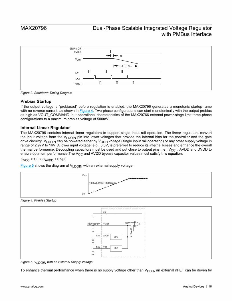
Prebias Startup If the output voltage is "prebiased" before regulation is enabled, the MAX20796 generates a monotonic startup ramp with no reverse current, as shown in Figure 4. Two-phase configurations can start monotonically with the output prebias as high as VOUT_COMMAND, but operational characteristics of the MAX20766 external power-stage limit three-phase configurations to a maximum prebias voltage of 500mV.
Internal Linear Regulator The MAX20796 contains internal linear regulators to support single input rail operation. The linear regulators convert the input voltage from the VLDOIN pin into lower voltages that provide the internal bias for the controller and the gate drive circuitry. VLDOIN can be powered either by VDDH voltage (single input rail operation) or any other supply voltage in range of 2.97V to 16V. A lower input voltage, e.g., 3.3V, is preferred to reduce its internal losses and enhance the overall thermal performance. Decoupling capacitors must be used and put close to output pins, i.e., VCC_, AVDD and DVDD to ensure optimum performance.The VCC and AVDD bypass capacitor values must satisfy this equation: CVCC < 1.3 × CAVDD + 0.9μF Figure 5 shows the diagram of VLDOIN with an external supply voltage.
0V
VOUT
PREBIAS ≤ VOUT_COMMAND
Figure 4. Prebias Startup
LDOVCC_
LDOAVDD
VLDOIN2.97V TO 16V
1.8V
1.8V
EB
VREF
Figure 5. VLDOIN with an External Supply Voltage
To enhance thermal performance when there is no supply voltage other than VDDH, an external nFET can be driven by
MAX20796 Dual-Phase Scalable Integrated Voltage Regulatorwith PMBus Interface
www.analog.com Analog Devices | 16

the EB pin to generate 3V to feed into the VLDOIN pin, as shown in Figure 6. The external nFET should be selected with sufficient power dissipation capability under the worst thermal case. SQA410EJ-T1_GE3 from Vishay is a good candidate to handle most of the application cases. A series resistor, of about 3Ω to 5Ω is needed on its drain terminal to limit the peak current when VDDH shuts down.
Restore Function (RESTORE) Upon a high-to-low transition of the RESTORE pin, VOUT is restored to the voltage set by PGMA. A 10µs deglitch time is employed to eliminate the possibility of a false RESTORE-low signal caused by noise coupling. The output voltage transition rate between the previous and new output voltage is the same rate as the transition between different VOUT_COMMAND voltages determined by TON_RISE/VOUT_COMMAND. Note that it is permissible for the system to hold the RESTORE signal low indefinitely. As long as RESTORE is low, the MAX20796 forces the restore function, which is: The device does not act on any command that directly changes the output voltage, except for bits 6 and 7 of the
OPERATION command that turns the supply on or off (0x00, 0x40, or 0x80); The device NACKs any VOUT_COMMAND data writes (and discards the new VOUT_COMMAND data), and the
corresponding STATUS_CML error flag (invalid data) is set.
LDOVCC_
LDOAVDD
VLDOIN
1.8V
1.8V
EB
4.5V TO 16V VDDH_
VREF
Figure 6. EB Drives a nFET to Generate 3V
Power Good (PGOOD) The PGOOD pin is an active-high, open-drain output that is used to show that VOUT has settled at the target voltage. PGOOD goes high after a fixed delay after the end of the startup transition (see the Electrical Characteristics table). PGOOD is deasserted if the output voltage drops below the PGOOD falling threshold relative to the nominal voltage for any reason.
Orthogonal Current Rebalancing (OCR) The MAX20796 implements an orthogonal current rebalancing (OCR) feature for enhanced dynamic-current sharing or balancing between different phase currents. This feature maintains current balance during load transients, even at a load-step frequency close to switching frequency or its harmonics. In the MAX20796, the OCR circuit adjusts the individual phase-current control signal from a common average current signal in order to minimize the phase-current imbalance. The individual phase- current control signal is conditioned through the OCR circuit before it reaches individual phase (PWM) modulator. This prevents each phase current from diverging from the average. For example, the new phase current control voltage for phase 1 is given as shown in Equation 1. Equation 1: VCPH1 = VC − ROCR × (IPH1 − IAVG) where,
MAX20796 Dual-Phase Scalable Integrated Voltage Regulatorwith PMBus Interface
www.analog.com Analog Devices | 17

VCPH1 = Phase 1 current-control signal, VC = Common average-current control signal, ROCR = OCR circuit gain resistance, IPH1 = Phase 1 current, and IAVG = Average current.
Synchronization Synchronizing multiple units can effectively reduce intermodulation noise and its interference to input current and output voltage. Up to four units of MAX20796 can be connected in the star connection format. The external synchronization clock is not necessary. Figure 7 shows the connection diagram without an external clock signal. In this case, Unit 1, by shorting its SYNC_IN pin to GND, is selected as the master to send out the synchronization clock signal to downstream units. Figure 7 shows how the four units can be connected if there is an external clock signal.
UNITUNIT11 UNITUNIT22 UNITUNIT33
SYNC_IN
SYNC_OUT
UNITUNIT44
MASTER(SYNC_IN=GND)
UNITUNIT11 UNITUNIT22 UNITUNIT33 UNITUNIT44
EXTERNAL CLOCK
SYNC_IN
SYNC_IN
SYNC_IN
SYNC_OUT
SYNC_OUT
SYNC_OUT
(a)
SYNC_IN
SYNC_IN
SYNC_IN
SYNC_IN
SYNC_OUT
SYNC_OUT
SYNC_OUT
SYNC_OUT
(b)
Figure 7. Synchronization Connection Diagram
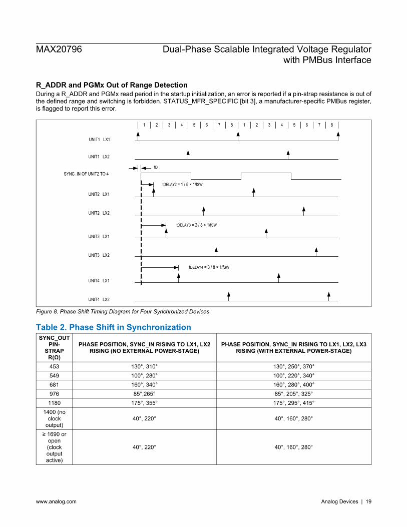
In addition to synchronization, an interleaving feature is included in the MAX20796. Figure 8 shows the phase-shift timing diagram in a four-unit system as in the Figure 7 (a) configuration. Unit 1 serves as the signal master and its SYNC_OUT is used as the input of Unit 2 to 4. After the SYNC_OUT pulldown resistor is read in the initialization period, each unit is assigned a fixed phase shift relative to its SYNC_IN input-signal rising edge. tD is the delay time from LX1 to its SYNC_OUT rising edge in Unit 1. Table 2 shows the SYNC_OUT pin-strap table. If the SYNC_IN signal is disqualified, e.g., the pulse is too narrow, out of lock-in range, or upon sudden loss of signal, the MAX20796 resumes switching smoothly with its pin-strap defined switching frequency.
Fault Handling
SNSP Open Detection The MAX20796 supports the SNSP pin open-detection at startup. If the SNSP pad or part of its feedback path is unconnected from the output for any reason, the regulator does not startup switching. This protection is only active at startup and is disabled in regulation.
MAX20796 Dual-Phase Scalable Integrated Voltage Regulatorwith PMBus Interface
www.analog.com Analog Devices | 18
R_ADDR and PGMx Out of Range Detection During a R_ADDR and PGMx read period in the startup initialization, an error is reported if a pin-strap resistance is out of the defined range and switching is forbidden. STATUS_MFR_SPECIFIC [bit 3], a manufacturer-specific PMBus register, is flagged to report this error.
UNIT1 LX1
1 2 3 4 5 6
SYNC_IN OF UNIT2 TO 4
tDELAY2 = 1 / 8 × 1/fSW
7 8 1 2 3 4 5 6 7 8
UNIT1 LX2
UNIT2 LX1
UNIT2 LX2
UNIT3 LX1
UNIT3 LX2
UNIT4 LX1
UNIT4 LX2
tD
tDELAY3 = 2 / 8 × 1/fSW
tDELAY4 = 3 / 8 × 1/fSW
Figure 8. Phase Shift Timing Diagram for Four Synchronized Devices
Table 2. Phase Shift in Synchronization SYNC_OUT
PIN- STRAP
R(Ω)
PHASE POSITION, SYNC_IN RISING TO LX1, LX2 RISING (NO EXTERNAL POWER-STAGE)
PHASE POSITION, SYNC_IN RISING TO LX1, LX2, LX3 RISING (WITH EXTERNAL POWER-STAGE)
453 130°, 310° 130°, 250°, 370° 549 100°, 280° 100°, 220°, 340° 681 160°, 340° 160°, 280°, 400° 976 85°,265° 85°, 205°, 325°
1180 175°, 355° 175°, 295°, 415° 1400 (no
clock output)
40°, 220° 40°, 160°, 280°
≥ 1690 or open (clock output active)
40°, 220° 40°, 160°, 280°
MAX20796 Dual-Phase Scalable Integrated Voltage Regulatorwith PMBus Interface
www.analog.com Analog Devices | 19

Overvoltage Protection (Tracking OVP) The MAX20796 overvoltage protection compares the output-feedback voltage to the VOUT_COMMAND value. If the output voltage exceeds VOUT_COMMAND plus the tracking OVP threshold (see the Electrical Characteristics table), an OVP fault is triggered, PGOOD is deasserted, and the device stops switching by turning off both highside and low-side FETs immediately. The OVP default response is “Shutdown and Retry” mode, which can also be changed through PMBus command, VOUT_OV_ FAULT_RESPONSE. In “Shutdown and Retry” mode, the system first shuts down switching, deasserts PGOOD, waits for about 50ms and then restarts if the OVP fault disappears. In “Ignore” mode, the system allows switching to continue, but deasserts PGOOD and flags in the corresponding bit in the STATUS_VOUT register. The OVP fault bit can be cleared by toggling the output enable state off and back on.
Undervoltage Protection (UVP) The MAX20796 undervoltage protection compares the output-feedback voltage to the VOUT_COMMAND value. If the output voltage is smaller than the VOUT_ COMMAND minus the UVP threshold (see the Electrical Characteristics table), an UVP fault is triggered, PGOOD is deasserted, and the device stops switching by turning off both high-side and low-side FETs immediately. The UVP default response is “Shutdown and Retry” mode, which can also be changed through the PMBus command, VOUT_UV_FAULT_RESPONSE. In “Shutdown and Retry” mode, the system first shuts down switching, deasserts PGOOD, waits for about 50ms and then restarts. In “Ignore” mode, the system just allows switching to continue, but deasserts PGOOD and flags the corresponding bit in STATUS register. The UVP fault bit can be cleared by toggling the output enable state off and back on.
Overvoltage Protection (Umbrella OVP) To gain a second level of protection, the absolute output voltage (VSNSP – VSNSN) is monitored and compared with fixed thresholds during operation. Two fixed thresholds, 2.5V or 6.0V, are set corresponding to VOUT_COMMAND in range of 0.5V to 2.437V or 2.438V to 5.0V, respectively. Both tracking and umbrella OVP mechanisms are handled by the same VOUT_OV_FAULT_RESPONSE and reported together as STATUS_VOUT [bit 7].
Overcurrent Protection (Average OCP) The total positive average current is compared to the number of phases times the per-phase OCP threshold defined by PGMD. Once an OCP fault is triggered, switching is shut down and PGOOD is deasserted. An OCP fault is not a latching fault and is registered in the fault log. Depending on the IOUT_OC_FAULT_RESPONSE command setting, the regulator begins “Shutdown and Retry” (factory default) after about 50ms or “Shutdown only” without restart. The shutdown and retry continues until the load current falls below the threshold.
Overcurrent Protection (Power Stage Peak OCP) Besides average OCP, the MAX20796 has the instantaneous cycle-by-cycle peak current protection in each power train. The internal lossless current sense technology is used and intended to operate only in extreme overcurrent conditions to protect the integrated FETs. Its threshold is fixed as shown in the Electrical Characteristics table. Once the power-stage peak OCP is triggered, the relevant phase turns off the high-side FET and turns on its low-side FET to keep its peak current at a safe level. Since the protection is based on the instantaneous current, the ripple current must be considered when calculating the maximum average current per phase. The maximum positive DC-phase current before clamping can be calculated as shown in Equation 2. Equation 2:
IPHASE_DC_MAX_POS = IPOCP_R −IPH_P − P
2 Where: IPH_P-P is the peak-to-peak phase-current ripple in the inductor. The MAX20796 also has a negative cycle-by-cycle overcurrent protection (NOCP) for each power train. Its threshold is also fixed as shown in the Electrical Characteristics table. If the NOCP threshold is reached, the low-side FET turns off and the high-side FET turns on for protection. Equation 3 shows the maximum negative DC current per phase. Equation 3:
IPHASE_DC_MAX_NEG = INOCP +IPH, PP
2
MAX20796 Dual-Phase Scalable Integrated Voltage Regulatorwith PMBus Interface
www.analog.com Analog Devices | 20
Undervoltage Lockout (UVLO) The MAX20796 includes UVLO circuits on the AVDD, VCC_, and VDDH_ supply input pins. The UVLO thresholds are specified in the Electrical Characteristics table. If a UVLO event is detected, the system stops regulating. Once the faulted input voltage rises above its UVLO rising threshold, the device reinitializes a new startup process.
Overtemperature Protection Overtemperature protection ensures the power train as well as the controller works within a safe temperature range. There are two temperatures monitored in the MAX20796. READ_TEMPERATURE_1 reports the integrated power train junction temperature. If there is an external power stage connected, READ_ TEMPERATURE_2 reports its junction temperature by monitoring the TS_FAULT pin voltage. If any temperature is over the programmed threshold, the fault is triggered. The regulator shuts down switching immediately by turning off both FETs, waiting for about 50ms off time, and then restarting if the junction temperature drops below threshold. STATUS_TEMPERATURE is flagged to report the fault. The factory default threshold is typically 150°C and it can be programmed using the PMBus commands. OT_FAULT_RESPONSE can be programmed to “Shutdown and Retry” (factory default) or “Shutdown only.”
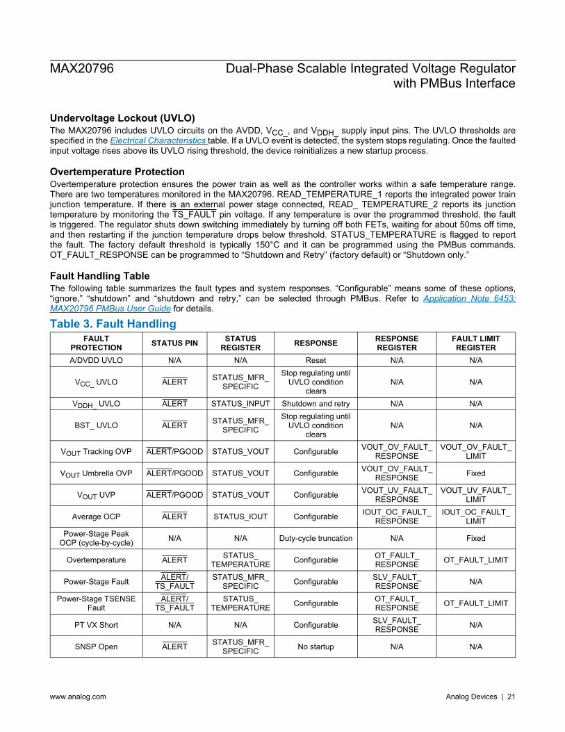
Fault Handling Table The following table summarizes the fault types and system responses. “Configurable” means some of these options, “ignore,” “shutdown” and “shutdown and retry,” can be selected through PMBus. Refer to Application Note 6453: MAX20796 PMBus User Guide for details.
Table 3. Fault Handling FAULT
PROTECTION STATUS PIN STATUS REGISTER RESPONSE RESPONSE
REGISTER FAULT LIMIT REGISTER
A/DVDD UVLO N/A N/A Reset N/A N/A
VCC_ UVLO ALERT STATUS_MFR_ SPECIFIC
Stop regulating until UVLO condition
clears N/A N/A
VDDH_ UVLO ALERT STATUS_INPUT Shutdown and retry N/A N/A
BST_ UVLO ALERT STATUS_MFR_ SPECIFIC
Stop regulating until UVLO condition
clears N/A N/A
VOUT Tracking OVP ALERT/PGOOD STATUS_VOUT Configurable VOUT_OV_FAULT_ RESPONSE
VOUT_OV_FAULT_ LIMIT
VOUT Umbrella OVP ALERT/PGOOD STATUS_VOUT Configurable VOUT_OV_FAULT_ RESPONSE Fixed
VOUT UVP ALERT/PGOOD STATUS_VOUT Configurable VOUT_UV_FAULT_ RESPONSE
VOUT_UV_FAULT_ LIMIT
Average OCP ALERT STATUS_IOUT Configurable IOUT_OC_FAULT_ RESPONSE
IOUT_OC_FAULT_ LIMIT
Power-Stage Peak OCP (cycle-by-cycle) N/A N/A Duty-cycle truncation N/A Fixed
Overtemperature ALERT STATUS_ TEMPERATURE Configurable OT_FAULT_
RESPONSE OT_FAULT_LIMIT
Power-Stage Fault ALERT/ TS_FAULT
STATUS_MFR_ SPECIFIC Configurable SLV_FAULT_
RESPONSE N/A
Power-Stage TSENSE Fault
ALERT/ TS_FAULT
STATUS_ TEMPERATURE Configurable OT_FAULT_
RESPONSE OT_FAULT_LIMIT
PT VX Short N/A N/A Configurable SLV_FAULT_ RESPONSE N/A
SNSP Open ALERT STATUS_MFR_ SPECIFIC No startup N/A N/A
MAX20796 Dual-Phase Scalable Integrated Voltage Regulatorwith PMBus Interface
www.analog.com Analog Devices | 21

Table 3. Fault Handling (continued) PGMx Out-of-Range
Fault ALERT STATUS_MFR_ SPECIFIC No startup N/A N/A
Nonvolatile PMBus Memory The MAX20796 features nonvolatile memory for storage of PMBus command values, which is only guaranteed to retain values correctly when written while VDDH is 10V to 16V, and while junction temperature is 0°C to 50°C. STORE_USER_ALL and STORE_INVENTORY commands are not sent when these conditions are not met.. The memory capacity is such that there are 5 possible storage “slots.” One slot can store most of the PMBus command sets. The contents of the “default” and “user” stores overrides pin‐strap command values where appropriate, according to the parameter loading‐precedence requirements of the PMBus specification. At any time, the number of remaining storage slots can be determined by reading the OTP_REMAINING command. Refer to Application Note 6453: MAX20796 PMBus User Guide for more information.
Pin-Strap Programmability
PMBus Address The PMBus address can be programmed by the R_ADDR resistor. 32 PMBus addresses can be pre-set by pin-strap.
Pin-Strap Output Voltage and VOUT_COMMAND The PGMA pin-strap resistor is used to set the output voltage, i.e., the initial value of VOUT_COMMAND. From 0.5V to 1.8V, each step is 50mV. Above 1.8V, only the commonly used rail voltages, e.g., 2.5V, 3.3V, and 5V can be programmed with direct feedback. To set the output voltage other than by the pin-strap resistor, either use VOUT_COMMAND through the PMBus interface or add a feedback divider to set the output voltage. Once VOUT_COMMAND is initially set by the pin-strap PGMA resistor or from nonvolatile memory, do not change the output voltage with VOUT_ COMMAND, or MARGIN_HIGH/LOW while regulating by more than ±25%. The slew rate for decreasing the output voltage must not exceed -0.5V/ms, as set by -VOUT_COMMAND/ TOFF_FALL. The slew rate for startup and shutdown can be higher than this value if desired. In the case, when output voltage is not included in the pin-strap table and VOUT_COMMAND is not available, the MAX20796 also supports the feedback divider method to set the arbitrary output voltage. The new output voltage can be calculated as: Equation 4:
VOUT = VDAC × (1 + R1 + R3R2 )
where R1 is the resistor between output and the SNSP pin, R3 is the resistor between ground and the SNSN pin, and R2 is the resistor between the SNSP and SNSN pins. R1 is equal to R3. VDAC is the setpoint voltage via pin-strap, (e.g., 0.6V or 1.0V, etc). Refer to Typical Application Circuit, where R1 = R10, R2 = R11, and R3 = R5. R1 and R2 are suggested to select small values (e.g., 100Ω or below) in order to avoid output voltage setting error caused by SNSP input bias current; (R1 + R3)// R2, or any series resistor on SNSP path should be much below 1.6kΩ to avoid falsely triggering SNSP open detection at startup. The resistors in the divider circuit must be sized appropriately to accommodate the power dissipation. Typically, 1/8W resistors are sufficient.
Voltage-Loop Gain and Zero Voltage loop compensation can be set by the PGMB pin-strap resistor. Eight different voltage-loop gains (IDES_GAIN) and four different voltage loop zeros (fZV) can be selected independently by this pin. To set a different voltage loop gain or zero, IDES_GAIN and F_ZERO commands can be used through the PMBus interface. Refer to Application Note 6453: MAX20796 PMBus User Guide for details.
MAX20796 Dual-Phase Scalable Integrated Voltage Regulatorwith PMBus Interface
www.analog.com Analog Devices | 22

Table 4. Pin-Strap Configurations R_ADDR PGMA PGMB PGMC PGMD PGME
BIN #
RNOM (Ω)
PMBus ADDRESS
VOUT_ COMMAND
(V)
IDES_ GAIN (V/V)
fZV (kHz)
RINT (Ω)
fZC (kHz)
PWM_RAMP SLEW RATE (V/µs)
POSITIVE AVERAGE OCP
THRESHOLD (PER PHASE)
(A)
TON_ RISE (ms)
FREQUENCY SWITCH
fSW (kHz)
0 37.4 0x10h 0.5 0.98 10.3 4522 5 0.425 10 0.5 200 1 45.3 0x11h 0.55 1.258 10.3 3668 5 0.425 13.3 0.5 308 2 54.9 0x12h 0.6 1.536 10.3 2964 5 0.425 16.7 0.5 400 3 68.1 0x13h 0.65 1.814 10.3 2209 5 0.425 20 0.5 444 4 82.5 0x14h 0.7 2.092 10.3 1761 5 0.425 23.3 0.5 500 5 97.6 0x15h 0.75 2.37 10.3 1257 5 0.425 26.7 0.5 571 6 118 0x16h 0.8 2.648 10.3 1098 5 0.425 30 0.5 666 7 140 0x17h 0.85 2.926 10.3 878 5 0.425 33.3 0.5 799 8 169 0x18h 0.9 0.98 16.5 4522 12.4 1.27 10 1 200 9 205 0x19h 0.95 1.258 16.5 3668 12.4 1.27 13.3 1 308
10 249 0x1Ah 1 1.536 16.5 2964 12.4 1.27 16.7 1 400 11 374 0x1Bh 1.05 1.814 16.5 2209 12.4 1.27 20 1 444 12 453 0x1Ch 1.1 2.092 16.5 1761 12.4 1.27 23.3 1 500 13 549 0x1Dh 1.15 2.37 16.5 1257 12.4 1.27 26.7 1 571 14 681 0x1Eh 1.2 2.648 16.5 1098 12.4 1.27 30 1 666 15 976 0x1Fh 1.25 2.926 16.5 878 12.4 1.27 33.3 1 799 16 1.18k 0x20h 1.3 0.98 19.6 4522 18 3.18 10 4 200 17 1.4k 0x21h 1.35 1.258 19.6 3668 18 3.18 13.3 4 308 18 1.69k 0x22h 1.4 1.536 19.6 2964 18 3.18 16.7 4 400 19 2.05k 0x23h 1.45 1.814 19.6 2209 18 3.18 20 4 444 20 2.49k 0x24h 1.5 2.092 19.6 1761 18 3.18 23.3 4 500 21 8.25k 0x25h 1.55 2.37 19.6 1257 18 3.18 26.7 4 571 22 9.76k 0x26h 1.6 2.648 19.6 1098 18 3.18 30 4 666 23 11.8k 0x27h 1.65 2.926 19.6 878 18 3.18 33.3 4 799 24 14.0k 0x28h 1.7 0.98 28.8 4522 21.9 4.46 10 8 200 25 16.9k 0x29h 1.75 1.258 28.8 3668 21.9 4.46 13.3 8 308 26 20.5k 0x2Ah 1.8 1.536 28.8 2964 21.9 4.46 16.7 8 400 27 24.9k 0x2Bh 2.5 1.814 28.8 2209 21.9 4.46 20 8 444 28 30.1k 0x2Ch 3.3 2.092 28.8 1761 21.9 4.46 23.3 8 500 29 37.4k 0x2Dh 5 2.37 28.8 1257 21.9 4.46 26.7 8 571 30 45.3k 0x2Eh 0.8 2.648 28.8 1098 21.9 4.46 30 8 666 31 54.9k 0x2Fh 0.7 2.926 28.9 878 21.9 4.46 33.3 8 799
Current-Loop Gain and Zero Current-loop compensation can be set by the PGMC pinstrap resistor. Eight different current-loop gains (RINT) and four different current-loop zeros (fZC) can be selected independently by this pin. Larger RINT gives higher current loop gain.
MAX20796 Dual-Phase Scalable Integrated Voltage Regulatorwith PMBus Interface
www.analog.com Analog Devices | 23

Compensation Ramp and OCP Thresholds An internal PWM ramp compensation is used to improve overall loop stability. Its slew rate can be programmed using the PGMD pin-strap resistor. This pin also sets up system average positive OCP thresholds, which is shown as per phase average current in the table. To get the total output current, the selected value needs to be multiplied by the actual phase count. To use other ramp slew rate values, the PWM_RAMP command can be used through the PMBus interface. Refer to Application Note 6453: MAX20796 PMBus User Guide for details.
Soft Time and Switching Frequency PGME pin-strap resistor can be used to program soft-start time (TON_RISE) and switching frequency (fSW). Four different soft-start times and eight different switching frequencies can be programmed with PGME. For other soft-start times, the TON_RISE command can be used through the PMBus interface. Refer to Application Note 6453: MAX20796 PMBus User Guide for details.
MAX20796 Dual-Phase Scalable Integrated Voltage Regulatorwith PMBus Interface
www.analog.com Analog Devices | 24

Application Circuit Design Procedure
Output Capacitor Selection The primary factors in determining the total required output capacitance (COUT) are the maximum allowable output voltage overshoot and undershoot (“sag” and “soar”) during load transients. In step-down converters, the voltage overshoot (ΔVOST) during unloading is the dominant factor in setting the required COUT because less forcing voltage is available to reduce the inductor current. For an unloading current-step (ΔI) and maximum allowed output-voltage overshoot (ΔVOST), the minimum required output capacitance can be estimated as in Equation 5. Equation 5:
COUT =( ∆ I
N +IPH_P − P
2 )2
× L × N
2 × ∆ VOsT × VOUT where: L = Inductance per phase N = Number of phases IPH_P-P = Peak-to-peak phase-current ripple in the inductor VOUT = Nominal output voltage Selecting a higher total COUT value increases design margin against component variation and effective capacitance loss due to voltage bias. For example, in a two-phase application, VDDH = 12V, VOUT = 0.8V, L = 100nH (coupled inductor), unloading step ∆I = 10A, ∆VOST = 3% of 0.8V input (= 24mV), the minimum AC capacitance can be calculated at 450µF. If any polymer capacitor is used, their equivalent-series resistance and inductance (ESR, ESL) cause output voltage ripple increase. Thus, sufficient capacitance margin and ceramic capacitors must be considered on the output side to further reduce the overshoot in order to meet the overall transient specs.
Output Inductor Selection For single-phase discrete inductors, the phase current peak-to-peak ripple (IPH_P-P is calculated as in Equation 6. Equation 6:
IPH_P − P =(VDDH − VOUT) × VOUT
fSW × L × VDDH For coupled inductors driven with duty cycle ≤ 1/N, the approximate inductor peak-to-peak phase-current ripple can be calculated as in Equation 7. Equation 7:
IPH_P − P =VOUT
fSW × L ( 1N −
VOUTVDDH
)
where: IPH_P-P = Peak-to-peak phase-current ripple in the inductor fSW = Switching frequency L = Inductance per phase N = Number of phases VDDH = Input voltage VOUT = Nominal output voltage A compromise should be made between output inductance and output capacitance. Too large of an inductance reduces current and voltage ripple, but still needs a larger output capacitance to suppress output voltage overshoot and
MAX20796 Dual-Phase Scalable Integrated Voltage Regulatorwith PMBus Interface
www.analog.com Analog Devices | 25

undershoot in the load transient. Usually 30% to 40% of IPH_P-P over the full load current is a good start point to design the application circuit. For example, in a two-phase application, VDDH = 12V, VOUT = 0.8V, L = 100nH (coupled inductor), fSW = 400kHz, IPH_P-P can be estimated to be 8.66A.
Input-Capacitor Selection The selection and placement of input capacitors are important considerations. High-frequency input capacitors serve to control switching noise. Bulk input capacitors are designed to filter the pulsed DC current that is drawn by the regulator. For the best performance, lowest cost and smallest size target, multilayer ceramic chip (MLCC) capacitors with 1210 or smaller case sizes, 47μF or smaller capacitance values, 16V or 25V voltage ratings, and X5R or better temperature characteristics are recommended as bulk. A high-frequency input capacitor should be placed as close as possible to the VDDH pins on the same side of PCB as the part. It is recommended to choose the bulk and MLCC input capacitance to control the peak-to-peak input voltage ripple to 2% to 3% of its nominal value. The minimum input capacitance in accordance with Equation 8 (suppose duty cycle ≤ 1/N). Equation 8:
CIN ≥IOUT_MAX × (VDDH − N × VOUT)
fSW × VDDH2 × VDDH_P − P
where: CIN = Input capacitance (MLCC) IOUT_MAX = Maximum load current N = Number of phases VDDH_P-P = Target peak-to-peak input voltage ripple Because the bulk input capacitors must source the pulsed DC-input current of the regulator, the power dissipation, and ripple-current rating for these capacitors are far more important than that for the output capacitors. The total RMS current that all input capacitors must withstand can be approximated using Equation 9. Equation 9:
IRMS_CIN =IOUT_MAX√VOUT × (VDDH / N − VOUT)
VDDH For example, in a two-phase application, VDDH = 12V, VOUT = 0.8V, L = 100nH (coupled inductor), fSW = 400kHz, IOUT, MAX = 40A and VDDH_P-P = ±3% x 12V (= 72mV), CIN AC capacitance can be estimated to be 80μF. Considering derating due to DC-bias voltage, the recommended minimum capacitance is 2 x 47μF (bulk) and 1.0μF + 0.1μF (high frequency) for each VDDH pin.
Internal Compensation (fZV, fZC, RINT, PWM Ramp, IDES_GAIN) Selection The MAX20796 uses peak current-mode control to simplify compensation design. The control loop can be stabilized by selecting appropriate IDES_GAIN values, fZV, fZC, RINT and PWM ramp slew rate under certain power stage parameters, e.g., L and COUT. No external compensation network is required. Voltage and current loop zeros should be selected smaller or equal to the power-stage double-pole frequency to compensate the phase delay, which can be estimated in Equation 10. Equation 10:
fZV, fZC ≤ 12π√ L
N × COUT For example, in a two-phase application (N = 2), VDDH = 12V, VOUT = 0.8V, L = 100nH (coupled inductor), fSW = 400kHz and COUT = 1mF, fZV, fZC < 22.5kHz. Usually, picking up lower frequency zeros, e.g., 10.3kHz to 16.5kHz, gains more phase margin. RINT sets the internal S/N ratio at the modulator within the limits of the allowed voltage swing across RINT (ΔV_ RINT), for which peak-to-peak voltage ΔV_RINT is 0.2V. Then the maximum RINT can be calculated with Equation 11 with a
MAX20796 Dual-Phase Scalable Integrated Voltage Regulatorwith PMBus Interface
www.analog.com Analog Devices | 26
duty cycle < 1/N. Equation 11:
RINT =2 × 10⁵ × L × fSW × ∆ V_RINT
VOUT × (1 − N ×VOUTVDDH
)
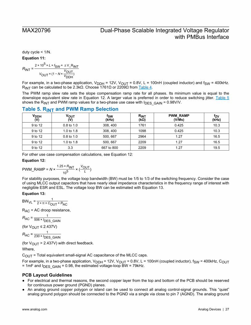
For example, in a two-phase application, VDDH = 12V, VOUT = 0.8V, L = 100nH (coupled inductor) and fSW = 400kHz. RINT can be calculated to be 2.3kΩ. Choose 1761Ω or 2209Ω from Table 4. The PWM ramp slew rate sets the slope compensation ramp rate for all phases. Its minimum value is equal to the downslope equivalent slew rate in Equation 12. A larger value is preferred in order to reduce switching jitter. Table 5 shows the RINT and PWM ramp values for a two-phase use case with IDES_GAIN = 0.98V/V.
Table 5. RINT and PWM Ramp Selection VDDH
(V) VOUT
(V) fSW
(kHz) RINT (kΩ)
PWM_RAMP (V/Μs)
fZV (kHz)
9 to 12 0.8 to 1.0 308, 400 1761 0.425 10.3 9 to 12 1.0 to 1.8 308, 400 1098 0.425 10.3 9 to 12 0.8 to 1.0 500, 667 2964 1.27 16.5 9 to 12 1.0 to 1.8 500, 667 2209 1.27 16.5 9 to 12 3.3 667 to 800 2209 1.27 19.5
For other use case compensation calculations, see Equation 12: Equation 12:
PWM_RAMP = N ×1.25 × RINT
105 × (VOUT
L )
For stability purposes, the voltage loop bandwidth (BW) must be 1/5 to 1/3 of the switching frequency. Consider the case of using MLCC output capacitors that have nearly ideal impedance characteristics in the frequency range of interest with negligible ESR and ESL. The voltage loop BW can be estimated with Equation 13. Equation 13:
BWVL = 12 × π × COUT × RAC
RAC = AC droop resistance,
RAC = 1506 × IDES_GAIN
(for VOUT ≤ 2.437V)
RAC = 1230 × IDES_GAIN
(for VOUT > 2.437V) with direct feedback. Where, COUT = Total equivalent small-signal AC capacitance of the MLCC caps. For example, in a two-phase application, VDDH = 12V, VOUT = 0.8V, L = 100nH (coupled inductor), fSW = 400kHz, COUT = 1mF and IDES_GAIN = 0.98, the estimated voltage-loop BW = 79kHz.
PCB Layout Guidelines For electrical and thermal reasons, the second copper layer from the top and bottom of the PCB should be reserved
for continuous power ground (PGND) planes. An analog ground copper polygon or island can be used to connect all analog control-signal grounds. This “quiet”
analog ground polygon should be connected to the PGND via a single via close to pin 7 (AGND). The analog ground
MAX20796 Dual-Phase Scalable Integrated Voltage Regulatorwith PMBus Interface
www.analog.com Analog Devices | 27

should be used as a shield and ground reference for the control signals (R_ ADDR, PGM_, PWM, SNSP, SNSN, and TS_FAULT).
The AVDD, DVDD decoupling capacitors should also be connected to the analog ground, and placed as close as possible to the AVDD and DVDD pin.
The VCC_ decoupling capacitors should also be connected to the PGND, and placed as close as possible to the VCC_ pins.
The pin-strap resistors (PGMA, PGMB, PGMC, PGMD, PGME, and R_ADDR) should be placed close to the IC and away from noisy signals.
Sufficient input capacitor should be used to mitigate the AC current flowing outside of the buck converter. The closest input decoupling capacitor should be located within 60 mils of the VDDH_ pins; otherwise, excessive spike
voltage induced at the VDDH_ pins increases voltage stress on the device significantly. Vias should not be used on the LX_ pin land pattern copper pour if the inductors are placed on the same side of the
PCB as the MAX20796. However, vias are preferred on the PGND_land pattern between the pin "fingers." Sufficient PGND vias are also needed close to the PGND_ pin pads.
The 0.22μF boost capacitors should be placed as close as possible to the LX_ and BST pins, on the same side of the PCB as the MAX20796.
PMBus Command Table 6 shows the supported PMBus command list. For the detailed PMBus command definition and its application note, refer to Application Note 6453: MAX20796 PMBus User Guide. The MAX20796 is available preconfigured for specific applications, as shown in Table 7.
Table 6. Supported PMBus Command List OPERATION STATUS_BYTE ON_OFF_CONFIG STATUS_WORD VOUT_MODE STATUS_VOUT VOUT_COMMAND STATUS_IOUT VOUT_TRIM STATUS_INPUT VOUT_MAX STATUS_TEMPERATURE VOUT_MARGIN_HIGH STATUS_CML VOUT_MARGIN_LOW STATUS_OTHER VOUT_MIN STATUS_MFR_SPECIFIC MFR_VOUT_MIN READ_VIN FREQUENCY_SWITCH READ_VOUT INTERLEAVE READ_IOUT TON_DELAY READ_TEMPERATURE_1 TON_RISE READ_TEMPERATURE_2 TOFF_DELAY TELEMETRY_ADDR TOFF_FALL TELEMETRY_DATA CLEAR_FAULTS LEAD_LAG VOUT_OV_FAULT_LIMIT IDES_GAIN VOUT_OV_FAULT_RESPONSE F_ZERO VOUT_OV_WARN_LIMIT ROCR_RINT VOUT_UV_WARN_LIMIT PWM_RAMP VOUT_UV_FAULT_LIMIT CAPABILITY VOUT_UV_FAULT_RESPONSE PMBUS_REVISION IOUT_OC_FAULT_LIMIT IC_DEVICE_ID IOUT_OC_FAULT_RESPONSE IC_DEVICE_REV
MAX20796 Dual-Phase Scalable Integrated Voltage Regulatorwith PMBus Interface
www.analog.com Analog Devices | 28

Table 6. Supported PMBus Command List (continued) IOUT_OC_WARN_LIMIT WRITE_PROTECT OT_FAULT_LIMIT STORE_USER_ALL OT_FAULT_RESPONSE RESTORE_USER_ALL OT_WARN_LIMIT OTP_REMAINING TON_MAX_FAULT_LIMIT STORE_INVENTORY TON_MAX_FAULT_RESPONSE FORCE_PEC SLV_FAULT_RESPONSE RESTORE_MAXIM_ALL SMBALERT_MASK
Table 7. Configuration Details PART
NUMBER DESCRIPTION COMMAND VALUE DATA
MAX20796 Unconfigured All commands Pin-strap, default Pin-strap, default
MAX20796A Scenario A
VOUT_COMMAND 1.000V 0x0200 VOUT_MAX 1.250V 0x0280 1.250V 0x0280
FREQUENCY_SWITCH 800kHz 0x0320 VOUT_OV_WARN_LIMIT 1.125V 0x0240 VOUT_UV_WARN_LIMIT 0.875V 0x01C0 IOUT_OC_WARN_LIMIT 54A 0xE360
TON_RISE 1ms 0xF004 LEAD_LAG 0.81/disabled/disabled 0x01
All other commands Default values Default values
MAX20796 Dual-Phase Scalable Integrated Voltage Regulatorwith PMBus Interface
www.analog.com Analog Devices | 29

Typical Application Circuits
Default schematic is for 3-ph board.For 2-ph board, change following components
1. L1 = CL1208-2-100TR-R2. R52 = 0_OHM3. R53 = 0_OHM4. U6 = DNI
8. R19 = 976_OHM7. R17 = 45.3_OHM6. C44 = DNI5. R49 = DNI
THE AGND PIN OF THE IC.THROUGH A SINGLE VIA CLOSE TOCONNECT AGND AND PGND PLANES
3PH / 2PH
ADDRESS: 0X11FREQUENCY_SWITCH: 308kHZVOUT_COMMAND: 0.8V
PWM_RAMP = 3.18V/us / 1.27V/usIDES_GAIN = 1.536 / 1.258
RINT: 2209_OHM TON_RISE=0.5msOCP LEVEL: 33.3A/phCURRENT_LOOP_ZERO: 12.4kHZVOLTAGE_LOOP_ZERO: 10.3kHZ
DNIDNI
DNI DNI DNI
DNI
DNI
DNI
DNI
DNI
DNI
TP28
R18
0R56
TP22
374
R_A
DD
R
TP24
R19
11.8
K R15 45
.3
PGM
E
65
43
21
L1
R5
R4
R25
C7
7 4
3
6 5 2 1 Q1
R17
R16
R20
R59
R58
R57
R55
R54
TP39
TP40TP38
TP37
R53
R52
TP36
TP35
TP34
TP33
TP32
C11
C1
TP3R
21TP
29
TP27TP26TP25TP23
C29C24
C18
5 4 3 2
1
J4
5 4 3 2
1
J3
R9
R8
C33
R13
C32
R11
R12
C31
C28
C26
C16
C15
C6
C5
C14
C13
C4
C3
C12
C2
C19
R1
C30
C21
C20
R14
R7
R10
R3
R2
C25
C17
C8
C23
C22
C9
C10
21
J1
21
J2
5
10
2
9
3
33
35
24
30
28
17
18
29
32
31
20
11
1
34
25
16
15
14
12
22
4
23
8
26
27
13
21
6
19
7
U1
47U
F
47U
F
22U
F
CL1208-3-100TR-R
SYNC_OUT
54.9
11845
.3
0
PGM
A
0
PGMA
22U
F
0.1U
F
PGMD
1UF
1UF
0.01
UF
0
SNSP
SYNC_IN
100P
F
0.1U
F
CS
PGM
C
PGM
D
0.1U
F
4700
PF
0.1U
F
LX2
RSP
0
0.22
UF
PGOOD
0
SNSN
LX1
0
SYNC_OUT
0.22UF
0.1U
F04.7U
F
4.7U
F
RESTORE_NEN
PGMB
4.7U
F
R_ADDR
PGMC
ALERT_N
47U
F
47U
F
VOU
T
4.7U
F
22U
F
SDA
PGME
MAX20796
3
SCL
VOUT_SENSE_P
4.7UF
0
VCC1P8
0.22UF
1UF
10
VOUT_SENSE_N
RSN
0
VIN
SQA410EJ-T1_GE3
FAULT_N
0
PREC
002S
AAN
-RC
VDD1P8
SYNC_IN
LX3
4.7UF
33
AUX3
P3
PREC
002S
AAN
-RC
PWM
0
22U
F
131-3701-266
0.1U
F0.
1UF
00
0
0
PGM
B
49.9
1.4K
4.7U
F4.
7UF
131-3701-266
0 0
SYNC_OUT
PGME TS_FAULTB
R_ADDR
SNSP
RESTOREB
SNSN
CS
DGND
PGMD
SYNC_IN
EB
LX1
PGOOD
ALERTB
SCL
SDA
PGMC
PGMB
PGMA
LX2
PGND2
DVDD
VLDOIN
EN
PGND1
BST1
PWM
BST2
VDDH2
VCC2
AGND
AVDD
VCC1
VDDH1
65
43
21
S
D
G
IO
IN
INIO
IOIOIOIOIO IO
IOIO
IO
IO
IO
IO
IO
IO
IO
IO
IO
IO
IO
IO
IO
IO
IO
IO
IO
IO
IO
IO
IO
MAX20796 Dual-Phase Scalable Integrated Voltage Regulatorwith PMBus Interface
www.analog.com Analog Devices | 30

Typical Application Circuits (continued)
OPTIONAL EXTERNAL POWER-STAGE
DNI
TP41
9
8
7
6
5432
1
12
11
16
13
15
10
14
U6
C98
C97
C96
C95
C94
C93
R50
R48
C10
2
R49
R47
C10
1
C99
C10
00.
1UF
1UF
VCC1P8
0.1U
F
0.1U
F
LX310
VIN
0.22
UF
1000
PF
LX3
CS
47U
F
PWM
FAULT_N
4.7
10
499
VDD1P8
MAX20766
47U
F
22U
F
22U
F
IO
TS_FAULTB
CS
AGN
D
PWM
VDD
VCC
BST
VX
VX
VX
VX
VSS
VSS
VSS
VSS
VDD
HIN
IO
IO
IO
IO
IO
IO
MAX20796 Dual-Phase Scalable Integrated Voltage Regulatorwith PMBus Interface
www.analog.com Analog Devices | 31

Typical Application Circuits (continued)
VIN SENSE POINT FOR EFFICIENCY MEASUREMENT
18 X 100uF 1206 MLCC, 6.3V
D1 TANT POLY
OS-CON, 10MM, 16VVIN SMB (DIVIDE BY 20)
INPUT AND OUTPUT BYPASS CAPACITANCE AND CONNECTORS
DNI
DNI
DNIDNIDNIDNIDNIDNIDNIDNI
DNIDNIDNIDNIDNIDNIDNI DNI
C59
100U
F
21
C27
C10
5
C10
4
C10
3
21
JP2
J8
J5
TP14
TP13
TP12
TP4
R29
R27
R22
C81
C80
C79
C78
C77
C76
C75
C74
C73
C72
21
C44
21
C43
21
C42
C71C67
C68
C69 C70
C66
C65
C64
C63
C62C61
C60
C58
C57
C56C55
C54
C53
C52C51
C48R28
6
5
4
3
2
1
ST2
6
5
4
3
2
1
ST1R26
CA
D2
CA
D1
21
C41
21
C40
21
C39
21
C38
21
C37
21
C36
TP9
TP8
3
2
1
J6
TP11
TP10
TP7
TP6
TP5
R23
C45
5 4 3 2
1
J9
5 4 3 2
1
J7
VOUT 100
100U
F
100U
F
100U
F
100U
F
100U
F
100U
F
100U
F
100U
F
330U
F
330U
F
100U
F
100U
F
100U
F
100U
F
PREC
002S
AAN
-RC
100U
F
100U
F
100U
F
100U
F
100U
F
100U
F
100U
F
100U
F
100U
F
100U
F
100U
F
100U
F
100U
F
52.3
131-3701-266
330U
F
100U
F
100U
F
VOU
T
MBR
S540
T3
100U
F
100U
F
1K
VOUT_SENSE_P
VOUT_SENSE_N 100P
F
0
49.9
131-3701-266
VIN
330U
F
100U
F
100U
F
100U
F
100U
F
MBR
S540
T3
0
PJ-102AH
6095
VIN_EFF_P
7808
330U
F
0.01
UF
7808
0.01
UF
VOU
T
100U
F
VIN_EFF_N6095
100U
F
VOU
T
VIN
100U
F
330U
F
IO
IO
+++
6
5
4
3
2
1
6
5
4
3
2
1
++++++
1
3
2
+
IN
IN
IN
IN
IN
Ordering Information PART TEMP RANGE PIN-PACKAGE CONFIGURATION
(TABLE 7) MAX20796GFB+ -40°C to +125°C 35 FC2QFN None
MAX20796GFB+T -40°C to +125°C 35 FC2QFN None MAX20796AGFB+ -40°C to +125°C 35 FC2QFN Scenario A
MAX20796AGFB+T -40°C to +125°C 35 FC2QFN Scenario A
+Denotes a lead(Pb)-free/RoHS-compliant package. T = Tape and reel.
MAX20796 Dual-Phase Scalable Integrated Voltage Regulatorwith PMBus Interface
www.analog.com Analog Devices | 32

Revision History REVISION NUMBER
REVISION DATE DESCRIPTION PAGES
CHANGED 0 7/18 Initial release —
1 2/19 Updated Benefit and Features, Absolute Maximum Ratings, Electrical Characteristics, Typical Operating Characteristics, Pin Description, Figure 2, Figure 3, Table 2, Detailed Description, Table 4, Table 6, and Typical Application Circuits
1, 3–5, 9, 13, 16, 17, 20, 22–25, 27–31
2 3/19 Updated Absolute Maximum Ratings, Electrical Characteristics table, and Detailed Description section
3–5, 15, 19,
21, 22, 25–28
3 11/19 Added MAX20796A preconfigured version. Corrected feedback circuit equation. Simplified Peak Overcurrent Protection symbols. Minor corrections and clarifications.
1, 3, 5, 17, 18, 21, 22,
28, 32
4 3/20 Added the PMBus nonvolatile memory commands and description. Clarified the VCC and AVDD bypass capacitor requirements.
1, 17, 21, 22, 28
5 12/21 Updated Package Information, Typical Operating Characteristics, and Applications Information section
7, 12–14, 33
Information furnished by Analog Devices is believed to be accurate and reliable. However, no responsibility is assumed by Analog Devices for its use, nor for any infringements of patents or other rights of third parties that may result from its use. Specifications subject to change without notice. No license is granted by implication or otherwise under any patent or patent rights of Analog Devices. Trademarks and registered trademarks are the property of their respective owners.
MAX20796 Dual-Phase Scalable Integrated Voltage Regulatorwith PMBus Interface
w w w . a n a l o g . c o m Analog Devices | 33