cmos 4-bit single chip microcomputer s5u1c6f666t11 … · 2007. 3. 27. · cn37 buzzer (bz1) (cn27)...
TRANSCRIPT

CMOS 4-BIT SINGLE CHIP MICROCOMPUTER
(S1C6F666/S1C05112 Demonstration Tool)S5U1C6F666T11 Manual

NOTICE
No part of this material may be reproduced or duplicated in any form or by any means without the written permission of Seiko Epson. Seiko Epson reserves the right to make changes to this material without notice. Seiko Epson does not assume any liability of any kind arising out of any inaccuracies contained in this material or due to its application or use in any product or circuit and, further, there is no representation that this material is applicable to products requir-ing high level reliability, such as medical products. Moreover, no license to any intellectual property rights is granted by implication or otherwise, and there is no representation or warranty that anything made in accordance with this mate-rial will be free from any patent or copyright infringement of a third party. This material or portions thereof may contain technology or the subject relating to strategic products under the control of the Foreign Exchange and Foreign Trade Law of Japan and may require an export license from the Ministry of International Trade and Industry or other approval from another government agency.
© SEIKO EPSON CORPORATION 2007, All rights reserved.
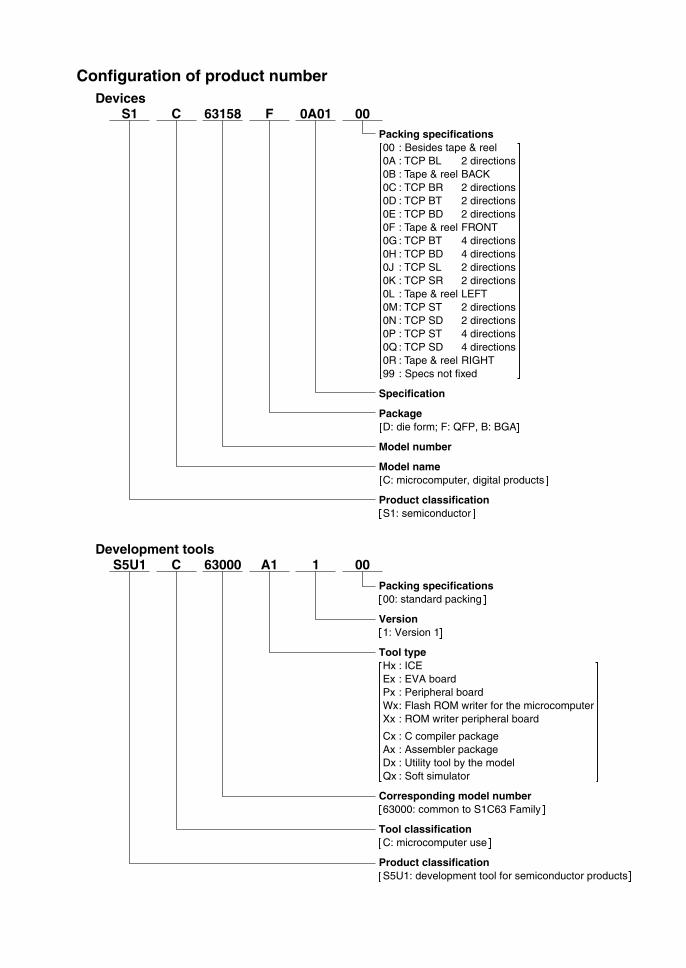
DevicesS1 C 63158 F 0A01
Packing specifications00 : Besides tape & reel0A : TCP BL 2 directions0B : Tape & reel BACK0C : TCP BR 2 directions0D : TCP BT 2 directions0E : TCP BD 2 directions0F : Tape & reel FRONT0G : TCP BT 4 directions0H : TCP BD 4 directions0J : TCP SL 2 directions0K : TCP SR 2 directions0L : Tape & reel LEFT0M: TCP ST 2 directions0N : TCP SD 2 directions0P : TCP ST 4 directions0Q : TCP SD 4 directions0R : Tape & reel RIGHT99 : Specs not fixed
Specification
PackageD: die form; F: QFP, B: BGA
Model number
Model nameC: microcomputer, digital products
Product classificationS1: semiconductor
Development toolsS5U1 C 63000 A1 1
Packing specifications00: standard packing
Version1: Version 1
Tool typeHx : ICEEx : EVA boardPx : Peripheral boardWx: Flash ROM writer for the microcomputerXx : ROM writer peripheral board
Cx : C compiler packageAx : Assembler packageDx : Utility tool by the modelQx : Soft simulator
Corresponding model number 63000: common to S1C63 Family
Tool classificationC: microcomputer use
Product classification S5U1: development tool for semiconductor products
00
00
Configuration of product number


CONTENTS
S5U1C6F666T11 MANUAL EPSON i(S1C6F666/S1C05112 DEMONSTRATION TOOL)
- PREFACE -
The S5U1C6F666 is a demonstration tool for the SEIKO EPSON S1C63 Family 4-bit single chip microcomputers.This manual explains the hardware specifications and how to use the S5U1C6F666.
- CONTENTS -
1 Overview ......................................................................................................................... 1
2 Names and Functions of Each Part ............................................................................. 22.1 S5U1C6F666 Main Board ................................................................................................. 3
2.2 S5U1C6F666 CPU Board ................................................................................................. 5
2.3 S5U1C6F666 EPD Board ................................................................................................. 7
2.4 S5U1C6F666 LCD Board .................................................................................................. 8
3 CPU System Configuration ........................................................................................... 93.1 Memory Map ..................................................................................................................... 9
3.2 Input/Output Port Functions ............................................................................................. 10
3.2.1 Input/Output Ports .............................................................................................. 103.2.2 LCD Segment Outputs ....................................................................................... 11
3.3 Mask Option ..................................................................................................................... 12
4 How to Use the S5U1C6F666 ....................................................................................... 144.1 Operating the S5U1C6F666 On a Stand-Alone Basis ..................................................... 14
4.1.1 Turning Power On/Off ......................................................................................... 144.1.2 Operation Check ................................................................................................ 144.1.3 Programming the PROM .................................................................................... 17
4.2 Connecting to ICE63 ........................................................................................................ 18
4.3 Customization .................................................................................................................. 19
5 Connector Pin Assignment ......................................................................................... 215.1 Main Board - CPU Board Interface Connectors ............................................................... 21
5.2 Main Board - Peripheral Board Interface Connectors ...................................................... 22
5.3 EPD Interface Connectors (EPD Board) .......................................................................... 23
6 Specifications ............................................................................................................... 25


1 OVERVIEW
S5U1C6F666T11 MANUAL EPSON 1(S1C6F666/S1C05112 DEMONSTRATION TOOL)
1 OverviewThe S5U1C6F666 is a demonstration tool for the SEIKO EPSON S1C63 Family 4-bit single chip microcomputers. The CPU board on the S5U1C6F666 is equipped with the S1C6F666. Thus user application programs can be run on the S5U1C6F666 by writing the program and data into the on-chip Flash memory of the S1C6F666. Further-more, the connector from which the CPU board is disconnected can be used to connect the S5U1C6F666 to the PRC board (S5U1C63000P1) installed in the ICE63 (S5U1C63000H1/S5U1C63000H2), this makes it possible to use the S5U1C6F666 for debugging application programs.All the S1C6F666 I/O signals are provided through the connectors and pads allowing connection of external parts or a user circuit board. The S5U1C6F666 supports development of various applications with flexibility.The following shows the S5U1C6F666 system configuration at shipment:
CPU: S1C6F666 Internal PROM = 16K words (An operation-check program is included.) Internal RAM = 5K words
OSC1 clock: Crystal oscillation 32.768 kHz
OSC3 clock: Ceramic oscillation 2.00 MHz
LCD panel: 8-digit 7-segment LCD Can be driven by the S1C6F666 on-chip LCD driver.
EPD driver: S1C05112 A 124-segment EPD panel can be driven. A DC-DC converter (3 V to 18 V) is built in.
Buzzer: A piezoelectric buzzer is mounted. Can be driven by the S1C6F666 BZ and BZ output ports.
Temperature and humidity measurement circuit: Can be measured by the S1C6F666 on-chip R/f converter. (External sensors are required.)

2 NAMES AND FUNCTIONS OF EACH PART
2 EPSON S5U1C6F666T11 MANUAL (S1C6F666/S1C05112 DEMONSTRATION TOOL)
2 Names and Functions of Each PartThe S5U1C6F666 consists of four boards: main board, CPU board, EPD board and LCD board.
SEIKO EPSON
S5U1C6F666T1100
Main board
CPU board
EPSONS1C6F666
CPU daughter boardSEIKO EPSON
S5U1C6F666T1100
∗
120SEG EPD daughter boardSEIKO EPSON S5U1C6F666T1100
S1C05112
EPD board
LCD board
Figure 2.1 S5U1C6F666
∗ The J4 jumper is set to OFF at shipment, change it to ON (short circuit) before using the S5U1C6F666.

2 NAMES AND FUNCTIONS OF EACH PART
S5U1C6F666T11 MANUAL EPSON 3(S1C6F666/S1C05112 DEMONSTRATION TOOL)
2.1 S5U1C6F666 Main BoardThis is the motherboard for mounting other daughter boards. The following shows the primary components that have been contained on the board.
SEIKO EPSON
S5U1C6F666T1100CN10 CN9
CN8 CN7
SW2SW1
SW5SW6
SW4
J1J2
SW3
CN26
CN36
CN37
Buzzer (BZ1)
(CN27)
Figure 2.1.1 Main Board
ICE interface connectors (CN1–CN4) The CPU board is inserted in these connectors at shipment. The connectors can also be used to connect the S5U1C6F666 to the ICE63. In this case, remove the CPU board
and connect between this connector and the I/O connector on the PRC board that has been installed in the ICE63 using the interface cable included with the PRC board. For the pin assignment of the connector, see Sec-tion 5.1, “Main Board - CPU Board Interface Connectors.” For how to connect to the ICE63, see Section 4.2, “Connecting to ICE63.”
EPD driver interface connector (CN26) The EPD board is inserted in this connector at shipment. The S1C6F666 I/O signals are assigned to the connector pins. For the pin assignment of the connector, see Sec-
tion 5.2, “Main Board - Peripheral Board Interface Connectors.”
LCD interface connectors (CN36, CN37) The LCD board is inserted in these connectors at shipment. The S1C6F666 LCD driver signals are assigned to the connector pins. Maximum 64 SEG × 8 COM of an LCD
panel can be driven through these connectors. For the pin assignment of the connector, see Section 5.2, “Main Board - Peripheral Board Interface Connectors.”
2 NAMES AND FUNCTIONS OF EACH PART
4 EPSON S5U1C6F666T11 MANUAL (S1C6F666/S1C05112 DEMONSTRATION TOOL)
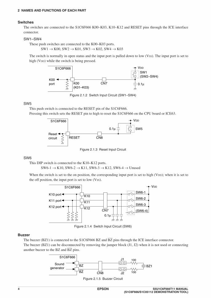
Switches The switches are connected to the S1C6F666 K00–K03, K10–K12 and RESET pins through the ICE interface
connector.
SW1–SW4 These push switches are connected to the K00–K03 ports. SW1 → K00, SW2 → K01, SW3 → K02, SW4 → K03
The switch is normally in open status and the input port is pulled down to low (VSS). The input port is set to high (VDD) while the switch is being pressed.
K00(K01–K03)
CN7
SW1(SW2–SW4)
0.1µ
VDD
K00port
S1C6F666
Figure 2.1.2 Switch Input Circuit (SW1–SW4)
SW5 This push switch is connected to the RESET pin of the S1C6F666. Pressing this switch sets the RESET pin to high to reset the S1C6F666 on the CPU board or ICE63.
RESET CN8
SW5
VDD
Resetcircuit
S1C6F666
0.1µ
Figure 2.1.3 Reset Input Circuit
SW6 This DIP switch is connected to the K10–K12 ports. SW6-1 → K10, SW6-2 → K11, SW6-3 → K12, SW6-4 → Unused
When the switch is set to the on position, the corresponding input port is set to high (VDD); when it is set to the off position, the input port is set to low (VSS).
K10
K11
K12CN7
SW6-1
SW6-2
SW6-3
(SW6-4)
VDD
K10 port
K11 port
K12 port
S1C6F666
0.1µ
Figure 2.1.4 Switch Input Circuit (SW6)
Buzzer The buzzer (BZ1) is connected to the S1C6F666 BZ and BZ pins through the ICE interface connector. The buzzer (BZ1) can be disconnected by removing the jumper block (J1, J2) when it is not used or connecting
another buzzer to the BZ and BZ pins.
BZ
BZ CN8
BZ1
J1 100
100J2
Soundgenerator
S1C6F666
Figure 2.1.5 Buzzer Circuit

2 NAMES AND FUNCTIONS OF EACH PART
S5U1C6F666T11 MANUAL EPSON 5(S1C6F666/S1C05112 DEMONSTRATION TOOL)
2.2 S5U1C6F666 CPU BoardThe CPU board is equipped with S1C6F666 and oscillation circuits. Also the board has ICE63 interface connectors for installing it to the main board.
On Board Writer interface connector (CN5)
Power switch(SW7)
Coin cell
EPSONS1C6F666
CPU daughter boardSEIKO EPSON
S5U1C6F666T1100
CN4
CPU
CN28 CN29
CN3 CN2 CN1
(Back)
J4
∗ The J4 jumper is set to OFF at shipment, change it to ON (short circuit) before using the S5U1C6F666.
Figure 2.2.1 CPU Board
CPU The SEIKO EPSON 4-bit single-chip microcomputer S1C6F666 is contained on the board. Refer to the
“S1C6F666 Technical Manual” for details of the S1C6F666.
Oscillation circuits The oscillator types and their frequencies are as follows: OSC1: Crystal resonator 32.768 kHz OSC3: Ceramic resonator 2.00 MHz
Battery holder (BAT1) Use a coin cell (2032 or 2016) as the power source.
R/f connectors (CN28, CN29) CN28 is connected to the S1C6F666 R/f pins (RFIN0, REF0, SEN0). Insert a temperature sensor (thermistor)
into this connector to configure a temperature measurement circuit. CN29 is connected to the S1C6F666 R/f pins (HUD, SEN1). Insert a humidity sensor into this connector to configure a humidity measurement circuit.
In order to customize the external R/f circuit according to the sensor to be used, pads are provided. For tem-perature/humidity sensors, contact SEIKO EPSON.
RFOUT
RFIN0
REF0
SEN0
RFIN1
REF1
SEN1
HUD
TP43
TP45
TP47
TP48
TP46
TP49
TP50
TP51 Pad
S1C6F666
1000p(CN45)10k1%
10k1%
(CN44)
CN28(temperature sensor)
1000p(CN43)
(CN41)
(CN40)
47k1%
10k1%
(CN42)
CN29(humidity sensor)
Figure 2.2.2 R/f Conversion Circuit
2 NAMES AND FUNCTIONS OF EACH PART
6 EPSON S5U1C6F666T11 MANUAL (S1C6F666/S1C05112 DEMONSTRATION TOOL)
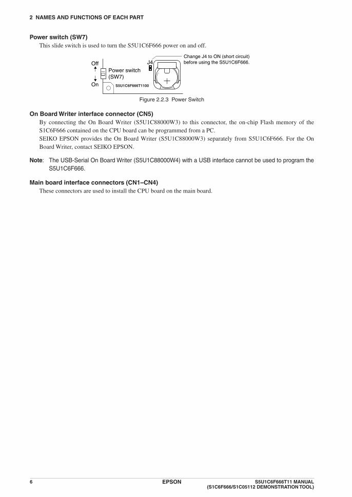
Power switch (SW7) This slide switch is used to turn the S5U1C6F666 power on and off.
Power switch(SW7)
On
Off
S5U1C6F666T1100
Change J4 to ON (short circuit) before using the S5U1C6F666.J4
Figure 2.2.3 Power Switch
On Board Writer interface connector (CN5) By connecting the On Board Writer (S5U1C88000W3) to this connector, the on-chip Flash memory of the
S1C6F666 contained on the CPU board can be programmed from a PC. SEIKO EPSON provides the On Board Writer (S5U1C88000W3) separately from S5U1C6F666. For the On
Board Writer, contact SEIKO EPSON.
Note: The USB-Serial On Board Writer (S5U1C88000W4) with a USB interface cannot be used to program the S5U1C6F666.
Main board interface connectors (CN1–CN4) These connectors are used to install the CPU board on the main board.

2 NAMES AND FUNCTIONS OF EACH PART
S5U1C6F666T11 MANUAL EPSON 7(S1C6F666/S1C05112 DEMONSTRATION TOOL)
2.3 S5U1C6F666 EPD BoardThe EPD board is equipped with an EPD driver IC.
120SEG EPD daughter boardSEIKO EPSON S5U1C6F666T1100
S1C05112
CN25(Back)
CN48CN47
CN46
EPD driver IC
Figure 2.3.1 EPD Board
EPD driver IC The EPD board is equipped with the SEIKO EPSON S1C05112 EPD driver. For details of the S1C05112, refer
to the “S1C05112 Technical Manual.”
EPD interface connectors (CN47, CN48) The EPD driver output signals are assigned to the connector pins. For the pin assignment of the connector, see
Section 5.3, “EPD Interface Connectors (EPD Board).”
EPD interface pads (CN46) The EPD driver output signals are assigned to the pads. For the signal assignment of the pads, see Section 5.3,
“EPD Interface Connectors (EPD Board).”
Main board interface connector (CN25) This connector is used to install the EPD board on the main board.

2 NAMES AND FUNCTIONS OF EACH PART
8 EPSON S5U1C6F666T11 MANUAL (S1C6F666/S1C05112 DEMONSTRATION TOOL)
2.4 S5U1C6F666 LCD BoardThe LCD board is equipped with an LCD panel.
LCD panel
CN38, CN39 (Back)
Figure 2.4.1 LCD Board
LCD panel The LCD board is equipped with a seven-segment LCD panel (LUMEX LCD-S801C42TR) that can display
eight-digit numbers by the outputs (COM0, SEG0–SEG63) from the S1C6F666 LCD driver. For the correspon-dence between the LCD segments and the LCD driver outputs, see Section 3.2.2, “LCD Segment Outputs.” For the correspondence between the display memory bits and the LCD driver outputs, see Section 3.3, “Mask Op-tion.”
Main board interface connectors (CN38, CN39) These connectors are used to install the LCD board on the main board.

3 CPU SYSTEM CONFIGURATION
S5U1C6F666T11 MANUAL EPSON 9(S1C6F666/S1C05112 DEMONSTRATION TOOL)
3 CPU System Configuration
3.1 Memory Map
0000H
3FFFH
Code PROM Code PROM Code PROM
When S1C63666 is selected(FFDFH•D2–D0 = 0)
0000H
3FFFH
When S1C63658 is selected(FFDFH•D2–D0 = 1)
0000H
3FFFH
When S1C63654 is selected(FFDFH•D2–D0 = 2)
Code PROM
0000H
3FFFH
S1C63656 is selected(FFDFH•D2–D0 = 4)
0000H
1400H
8000H
9000H
F000H
F0A0H
FF00H
FFFFH
RAM
Unused area
Unused area
Data PROM
Display memory
Unused area
I/O memory
0000H
0400H
8000H
9000H
F000H
F0A0H
FF00H
FFFFH
RAM
Unused area
RAM
Unused area
Unused area
Data PROM
Display memory
Unused area
I/O memory
0000H
0200H
8000H
9000H
F000H
F0A0H
FF00H
FFFFH
RAM
Unused area
Unused area
Data PROM
Display memory
Unused area
I/O memory
0000H
0400H
8000H
9000H
F000H
F0A0H
FF00H
FFFFH
Unused area
Data PROM
Display memory
Unused area
I/O memory
Figure 3.1.1 Memory Map
The code PROM size is 16,384 × 13 bits (16K words).The data PROM size is 4,094 × 4 bits (4K words).For details of the PROM, refer to the “S1C6F666 Technical Manual.”

3 CPU SYSTEM CONFIGURATION
10 EPSON S5U1C6F666T11 MANUAL (S1C6F666/S1C05112 DEMONSTRATION TOOL)
3.2 Input/Output Port Functions
3.2.1 Input/Output Ports
Table 3.2.1.1 lists the S1C6F666 input/output pins used in the S5U1C6F666 and their connection destinations. (See Section 3.2.2 for the LCD driver pins.)
Table 3.2.1.1 S1C6F666 Input/Output Pins Used Pin No. Port name I/O Connection destination
78 K00 I SW1 (Main board)79 K01 I SW2 (Main board)80 K02 I SW3 (Main board)81 K03 I SW4 (Main board)82 K10 I SW6-1 (Main board)83 K11 I SW6-2 (Main board)84 K12 I SW6-3 (Main board)102 BZ O Buzzer (pin 1) (Main board)103 XBZ O Buzzer (pin 2) (Main board)86 P00 O SDAT0 (EPD board)87 P01 O SDAT1 (EPD board)88 P02 O SDAT2 (EPD board)89 P03 O SDAT3 (EPD board)90 P10 O SEN (EPD board)91 P11 O XCS (EPD board)92 P12 O SCK (EPD board)93 P13 O DIV (NC)94 R00 O LO_ACT (EPD board)95 R01 O DD_ACT (EPD board)97 R03/FOUT O DCK (EPD board)98 R10 O DD0: Fix at VSS (EPD board)*99 R11 O DD1: Fix at VSS (EPD board)*21 SEN1 O Humidity sensor (CPU board)22 HUD O Humidity sensor (CPU board)19 SEN0 O Temperature sensor (CPU board)18 REF0 O Temperature sensor (CPU board)16 RFIN0 I Temperature sensor (CPU board)36 RESET I SW5 (Main board)
∗ The R10 and R11 ports must be fixed at low (VSS).
For how to control the input/output ports and R/f converter, refer to the “S1C6F666 Technical Manual.” For how to control the EPD driver, refer to the “S1C05112 Technical Manual.”

3 CPU SYSTEM CONFIGURATION
S5U1C6F666T11 MANUAL EPSON 11(S1C6F666/S1C05112 DEMONSTRATION TOOL)
3.2.2 LCD Segment Outputs
The LCD panel is driven with the COM0 and SEG0–SEG63 outputs. The S5U1C6F666 LCD board does not use the COM1–COM7 outputs.Figure 3.2.2.1 shows the correspondence between the segment output signals and the LCD segments. For the cor-respondence between the segment outputs and the display memory bits, see “Segment option” in Section 3.3, “Mask Option.”
SEG59COM0
SEG61
SE
G62
SE
G60
SE
G56
SE
G58
SEG63
SEG57SEG44
SEG46
SE
G47
SE
G45
SE
G41
SE
G43
SEG48
SEG42SEG3
SEG5
SE
G6
SE
G4
SE
G0
SE
G2
SEG7
SEG1SEG11
SEG13
SE
G14
SE
G12
SE
G32
SE
G8
SE
G10
SEG15
SEG9SEG19
SEG21
SE
G22
SE
G20
SE
G16
SE
G18
SEG23
SEG17SEG27
SEG29
SE
G30
SE
G28
SE
G24
SE
G26
SEG31
SEG25SEG36
SEG38
SE
G39
SE
G37
SE
G33
SE
G35
SEG40
SEG34
SEG53
SE
G54
SE
G52
SE
G49
SE
G51
SEG55
SEG50
Figure 3.2.2.1 Correspondence between Segment Outputs and LCD Segments
When using the S5U1C6F666 LCD board, set up the S1C6F666 as below.Target model: S1C63666 (FFDFH•D0–D2 = 000)LCD drive duty: 1/4 duty (FF60H•D2, D3 = 00)

3 CPU SYSTEM CONFIGURATION
12 EPSON S5U1C6F666T11 MANUAL (S1C6F666/S1C05112 DEMONSTRATION TOOL)
3.3 Mask OptionThe S1C6F666 contained on the CPU board is the Type B standard mask option model.
Standard mask option (Type B)1. OSC1 SYSTEM CLOCK ■ 1. Crystal
2. OSC3 SYSTEM CLOCK ■ 2. Ceramic
3. SVD EXTERNAL VOLTAGE DETECTION ■ 1. Not Use
4. INPUT PORT PULL DOWN RESISTOR • K00 .................■ 1. With Resistor • K01 .................■ 1. With Resistor • K02 .................■ 1. With Resistor • K03 .................■ 1. With Resistor • K10 .................■ 1. With Resistor • K11 .................■ 1. With Resistor • K12 .................■ 1. With Resistor • K13 .................■ 1. With Resistor
5. RESET PORT PULL DOWN RESISTOR • RESET ............■ 1. With Resistor
6. I/O PORT PULL DOWN RESISTOR • P00 ..................■ 1. With Resistor • P01 ..................■ 1. With Resistor • P02 ..................■ 1. With Resistor • P03 ..................■ 1. With Resistor • P10 ..................■ 1. With Resistor • P11 ..................■ 1. With Resistor • P12 ..................■ 1. With Resistor • P13 ..................■ 1. With Resistor
7. OUTPUT PORT OUTPUT SPECIFICATION • R00 .................■ 1. Complementary • R01 .................■ 1. Complementary • R02 .................■ 1. Complementary • R03 .................■ 1. Complementary • R10 .................■ 1. Complementary • R11 .................■ 1. Complementary • R12 .................■ 1. Complementary • R13 .................■ 1. Complementary
8. I/O PORT OUTPUT SPECIFICATION • P00 ..................■ 1. Complementary • P01 ..................■ 1. Complementary • P02 ..................■ 1. Complementary • P03 ..................■ 1. Complementary • P10 ..................■ 1. Complementary • P11 ..................■ 1. Complementary • P12 ..................■ 1. Complementary • P13 ..................■ 1. Complementary
9. MULTIPLE KEY ENTRY RESET COMBINATION ■ 1. Not Use
10. MULTIPLE KEY ENTRY RESET TIME AUTHORIZE ■ 1. Not Use
11. LCD DRIVING POWER ■ 1. Internal Power (3.0 V panel)

3 CPU SYSTEM CONFIGURATION
S5U1C6F666T11 MANUAL EPSON 13(S1C6F666/S1C05112 DEMONSTRATION TOOL)
12. SEGMENT OPTION
H: RAM data high-order address (0–9) L: RAM data low-order address (0–F) D: Data bit (0–3)
Pin name
SEG0SEG1SEG2SEG3SEG4SEG5SEG6SEG7SEG8SEG9SEG10SEG11SEG12SEG13SEG14SEG15SEG16SEG17SEG18SEG19SEG20SEG21SEG22SEG23SEG24SEG25SEG26SEG27SEG28SEG29SEG30SEG31SEG32SEG33SEG34SEG35SEG36SEG37SEG38SEG39SEG40SEG41SEG42SEG43SEG44SEG45SEG46SEG47SEG48SEG49SEG50SEG51SEG52SEG53SEG54SEG55SEG56SEG57SEG58SEG59SEG60SEG61SEG62SEG63
H0000000011111111222222223333333344444444555555556666666677777777
L02468ACE02468ACE02468ACE02468ACE02468ACE02468ACE02468ACE02468ACE
D0000000000000000000000000000000000000000000000000000000000000000
COM0Address (F0xx)
H0000000011111111222222223333333344444444555555556666666677777777
L02468ACE02468ACE02468ACE02468ACE02468ACE02468ACE02468ACE02468ACE
D1111111111111111111111111111111111111111111111111111111111111111
COM1H0000000011111111222222223333333344444444555555556666666677777777
L02468ACE02468ACE02468ACE02468ACE02468ACE02468ACE02468ACE02468ACE
D2222222222222222222222222222222222222222222222222222222222222222
COM2H0000000011111111222222223333333344444444555555556666666677777777
L02468ACE02468ACE02468ACE02468ACE02468ACE02468ACE02468ACE02468ACE
D3333333333333333333333333333333333333333333333333333333333333333
COM3H0000000011111111222222223333333344444444555555556666666677777777
L13579BDF13579BDF13579BDF13579BDF13579BDF13579BDF13579BDF13579BDF
D0000000000000000000000000000000000000000000000000000000000000000
COM4H0000000011111111222222223333333344444444555555556666666677777777
L13579BDF13579BDF13579BDF13579BDF13579BDF13579BDF13579BDF13579BDF
D1111111111111111111111111111111111111111111111111111111111111111
COM5H0000000011111111222222223333333344444444555555556666666677777777
L13579BDF13579BDF13579BDF13579BDF13579BDF13579BDF13579BDF13579BDF
D2222222222222222222222222222222222222222222222222222222222222222
COM6H0000000011111111222222223333333344444444555555556666666677777777
L13579BDF13579BDF13579BDF13579BDF13579BDF13579BDF13579BDF13579BDF
D3333333333333333333333333333333333333333333333333333333333333333
COM7
S1C
6365
4S
1C63
656
S1C
6365
8S
1C63
666

4 HOW TO USE THE S5U1C6F666
14 EPSON S5U1C6F666T11 MANUAL (S1C6F666/S1C05112 DEMONSTRATION TOOL)
4 How to Use the S5U1C6F666
4.1 Operating the S5U1C6F666 On a Stand-Alone BasisThe S5U1C6F666 can be operated on a stand-alone basis by the program that is written in the on-chip PROM of the S1C6F666 contained on the CPU board. An operation check program that was written into the PROM at shipment can be executed. Furthermore, user programs can be written to the PROM using the On Board Writer (S5U1C88000W3) to execute. The following explains how to control stand-alone operations.
4.1.1 Turning Power On/Off
The S5U1C6F666 operates with the battery on the CPU board. Set a coin cell (2032 or 2016) into the battery hold-er. Use the power switch (SW7) on the CPU board to turn the power on and off.
Power switch(SW7)
On
Off
S5U1C6F666T1100
J4
Figure 4.1.1.1 Power On/Off
When the power is turned on, the program written in the S1C6F666 PROM starts running.
Notes: • The J4 jumper is set to OFF at shipment, change it to ON (short circuit) before using the S5U1C6F666.
• Make sure that the S5U1C6F666 boards are installed properly before turning the S5U1C6F666 on.
4.1.2 Operation Check
This section describes how to use the operation check program that was written into the S1C6F666 PROM at ship-ment.Although a factory inspection has been performed, run this program to check whether the S5U1C6F666 operates normally or not before rewriting the program in the S1C6F666 PROM.
The operation-check program performs an input test using SW1–4. (SW5 is the reset switch.)When a switch is pressed, the switch number is displayed on the LCD panel and at the same time the buzzer sounds.The following is the operation procedure:
(1) Turning power on The LCD panel displays “in: ”.
Figure 4.1.2.1 LCD Display at Power On (Initial Screen)

4 HOW TO USE THE S5U1C6F666
S5U1C6F666T11 MANUAL EPSON 15(S1C6F666/S1C05112 DEMONSTRATION TOOL)
(2) Switch operation (port input) and buzzer output check When SW1 is pressed, the LCD panel displays “in:01” and the buzzer sounds. When SW2 is pressed, the LCD panel displays “in:02” and the buzzer sounds. When SW3 is pressed, the LCD panel displays “in:03” and the buzzer sounds. When SW4 is pressed, the LCD panel displays “in:04” and the buzzer sounds.
Figure 4.1.2.2 LCD Display when a Switch is Pressed (SW1)
Check to see if the pressed switch number is displayed properly. After SW1, SW2 or SW3 is pressed, the EPD driver check (step 3 below) can be performed. After SW4 is pressed, the LCD display check (step 4 below) can be performed. The R/f operation check (step 5 below) can be performed regardless of the switch pressed.
(3) EPD driver check Press SW1, SW2 or SW3 and then monitor the signal on the EPD driver’s segment pin (pin 124) using measur-
ing equipment such as an oscilloscope. The table below lists the relationship between the switch and the segment output status.
Table 4.1.2.1 EPD Driver CheckSwitch EPD segment output status
SW1 All segment outputs go high.SW2 All segment outputs go low.SW3 Toggles between high and low.
(4) LCD display check Check the display contents on the LCD panel after pressing SW4. The LCD panel displays the numbers below.
Each digit shifts to the left in 1-second cycles.
↓
↓
↓
Figure 4.1.2.3 LCD Display Check
Check to see if the numbers are displayed properly. To quit the check, press the RESET switch (SW5). The LCD display goes back to the initial screen.

4 HOW TO USE THE S5U1C6F666
16 EPSON S5U1C6F666T11 MANUAL (S1C6F666/S1C05112 DEMONSTRATION TOOL)
(5) R/f operation check The R/f operation check can be performed regardless of the switch pressed. Monitor the SEN0 and REF0 signals using measuring equipment such as an oscilloscope, and check to see if
rectangular wave signals are being output.
EPSONS1C6F666
CPU daughter boardSEIKO EPSON
CN28
CN45
(Monitor the right pins on CN28 and CN45.)
Figure 4.1.2.4 Monitor Position for R/f Operation Check
CH1 10:12.00 V/divDC FullCH2 10:12.00 V/divDC Full
Edge CH1Normal1.22 V
Normal20kS/s 50MS/div
CN45
CN28
Figure 4.1.2.5 Monitored Signals During R/f Operation Check
(6) To finish the operation check Turn the power off.

4 HOW TO USE THE S5U1C6F666
S5U1C6F666T11 MANUAL EPSON 17(S1C6F666/S1C05112 DEMONSTRATION TOOL)
4.1.3 Programming the PROM
The CPU board provides the connector to connect the S5U1C6F666 to the On Board Writer (S5U1C88000W3) al-lowing the user to program the S1C6F666 PROM.
RS-232Cinterface cable
S5U1C88000W3(On Board Writer)
COMx
SIO cable
SEIKO EPSON
S5U1C6F666T1100
EPSONS1C6F666
CPU daughter boardSEIKO EPSON
S5U1C6F666T1100
120SEG EPD daughter boardSEIKO EPSON S5U1C6F666T1100
S1C05112
Figure 4.1.3.1 PROM Programming System
Notes: • The S5U1C6F666 supports only the On Board Writer (S5U1C88000W3) with an RS-232C in-terface.
The USB-Serial On Board Writer (S5U1C88000W4) with a USB interface cannot be used.
• The target board must supply a 4.5 V to 5.0 V operating voltage to the On Board Writer (S5U1C88000W3) when programming the PROM. Supply a 4.5 V to 5.0 V operating voltage to the terminal of the battery holder. Be sure to remove the battery from the CPU board before supplying the operating voltage.
The tools below are required for PROM programming.• On Board Writer (S5U1C88000W3)• On Board Writer Control Software (OBPW63.EXE, RW6F666.INI) *
* The On Board Writer Control Software is included in the S1C63 Family Assembler Package 2 (S5U1C63000A2) or later.
After the program has been completed, execute the HEX converter HX63 to create the HEX data files (C3xxxyyy.HSA, C3xxxyyy.LSA, C3xxxyyy.CSA) from the object file (C3xxxyyy.ABS). Then write the created HEX data files into the S1C6F666 using the On Board Writer Control Software.Refer to the “S1C6F666 Technical Manual” for more information on the PROM programming.

4 HOW TO USE THE S5U1C6F666
18 EPSON S5U1C6F666T11 MANUAL (S1C6F666/S1C05112 DEMONSTRATION TOOL)
4.2 Connecting to ICE63The S5U1C6F666 from which the CPU board was removed can be connected to an ICE63 (S5U1C63000H1/ S5U1C63000H2) as a target board and used for debugging programs.
Note: Be sure to turn the S5U1C6F666 and ICE63 off before connecting/disconnecting the CPU board and I/O cables.
Use the I/O cables (80pin - 40pin × 2, 100pin - 50pin × 2, flat type) supplied with the S5U1C63000P1 (installed in the ICE63) for the connection.Connect the CN7–CN10 connectors on the S5U1C6F666 main board to the CN1 and CN2 connectors on the S5U1C63000P1 as shown in Figure 4.2.1.
SEIKO EPSON
S5U1C6F666T1100
120SEG EPD daughter boardSEIKO EPSON S5U1C6F666T1100
S1C05112
1
TRGOUTPC 0
STOPOUT
TRC IN
BRK INGND
2 3 4 5 6 7 8 ICERUN RS232C
S5U1C63000H2 EPSONPC 1
PC 2PC 3
PC 4PC 5
PC 6PC 7
PC 8PC 9
PC 10
PC 11
PC 12
PC 13
PC 14
PC 15
SLP/H
LTEM
U
POWER
CN2S5U1C63000P1
CN1
CN10 CN9CN8 CN7
(100pin) (80pin)
CN2-2(50pin)
CN1-1(40pin)
CN1-2(40pin)
CN2-1(50pin)
Figure 4.2.1 Connecting to ICE63 (S5U1C63000P1)
When an ICE63 is connected, the ICE63 supplies the power to the S5U1C6F666.
Note: The S1C6F666 functions that are not supported by the target model cannot be used when the S5U1C6F666 is being operated with an ICE63.
S1C63666/63808 The R/f converter does not supports AC bias operation. S1C63654 The integer multiplier is not available. S1C63808 The LCD driver is not available. For more information, refer to the technical manual for the target model.

4 HOW TO USE THE S5U1C6F666
S5U1C6F666T11 MANUAL EPSON 19(S1C6F666/S1C05112 DEMONSTRATION TOOL)
4.3 CustomizationThe S5U1C6F666 can also be used as a tool for developing user programs. In order to configure the system re-quired for the application, the S5U1C6F666 allows customization by using the pads or replacing the peripheral board.However customization should be performed at user’s own risk.
Note: Be sure to remove the battery before reconfiguration or modification of the boards is performed. Make sure that the power is off when changing the jumper settings.
Input/output ports and comparator inputs The main board provides the pads (CN27) for a 50-pin connector. Connect the user input/output signals to these
pads or mount a connector to install the user I/O circuit board. For the signal assignment of the pads, see Section 5.2, “Main Board - Peripheral Board Interface Connectors.”
Note: As described in Section 3.2.1, “Input/Output Ports,” the P00–P03, P10–P13, R00, R01, R03, R10, and R11 ports are used for the EPD driver. Therefore, these ports cannot be used when the EPD board is used. When the application requires these ports, the EPD board must be removed.
Motor driver outputs The CPU board provides the pads (TP38–TP41) to pull out the motor driver output from the S1C6F666. AO1 → TP41, AO2 → TP40, BO1 → TP39, BO2 → TP38
EPSONS1C6F666
CN38 CN40
CN39 CN41
Figure 4.3.1 Motor Driver Output Pads
R/f conversion circuit CN28 on the CPU board is connected to the S1C6F666 R/f pins (RFIN0, REF0, SEN0). Insert a temperature
sensor (thermistor) into this connector to configure a temperature measurement circuit. CN29 is connected to the S1C6F666 R/f pins (HUD, SEN1). Insert a humidity sensor into this connector to configure a humidity measurement circuit.
In order to customize the external R/f circuit according to the sensor to be used, pads are provided.
RFOUT
RFIN0
REF0
SEN0
RFIN1
REF1
SEN1
HUD
TP43
TP45
TP47
TP48
TP46
TP49
TP50
TP51 Pad
S1C6F666
1000p(CN45)10k1%
10k1%
(CN44)
CN28(temperature sensor)
1000p(CN43)
(CN41)
(CN40)
47k1%
10k1%
(CN42)
CN29(humidity sensor)
Figure 4.3.2 R/f Conversion Circuit

4 HOW TO USE THE S5U1C6F666
20 EPSON S5U1C6F666T11 MANUAL (S1C6F666/S1C05112 DEMONSTRATION TOOL)
LCD panel The S1C6F666 LCD driver output signals are assigned to CN36 and CN37 on the main board. When replacing
the LCD panel, remove the S5U1C6F666 LCD board from these connectors and install the user LCD board. For the pin assignment of the connectors, see Section 5.2, “Main Board - Peripheral Board Interface Connec-
tors.”

5 CONNECTOR PIN ASSIGNMENT
S5U1C6F666T11 MANUAL EPSON 21(S1C6F666/S1C05112 DEMONSTRATION TOOL)
5 Connector Pin Assignment
5.1 Main Board - CPU Board Interface Connectors
Note: Some “NC” pins are connected on the main board.
CN7 CN8 CN9 CN10No. Pin name No. Pin name No. Pin name No. Pin name1 VDD 1 VDD 1 COM0 1 SEG422 VDD 2 VDD 2 COM1 2 SEG433 K00 3 R00 3 COM2 3 SEG444 K01 4 R01 4 COM3 4 SEG455 K02 5 R02 5 COM4 5 SEG466 K03 6 R03 6 COM5 6 SEG477 K10 7 R10 7 COM6 7 SEG488 K11 8 R11 8 COM7 8 SEG499 K12 9 R12 9 SEG0 9 SEG5010 K13 10 R13 10 SEG1 10 SEG5111 VSS 11 VSS 11 SEG2 11 SEG5212 VSS 12 VSS 12 SEG3 12 SEG5313 P00 13 BZ 13 SEG4 13 SEG5414 P01 14 BZ 14 SEG5 14 SEG5515 P02 15 NC 15 SEG6 15 SEG5616 P03 16 NC 16 SEG7 16 SEG5717 P10 17 NC 17 SEG8 17 SEG5818 P11 18 NC 18 SEG9 18 SEG5919 P12 19 NC 19 SEG10 19 SEG6020 P13 20 NC 20 SEG11 20 SEG6121 VDD 21 VDD 21 SEG12 21 SEG6222 VDD 22 VDD 22 SEG13 22 SEG6323 NC 23 NC 23 SEG14 23 SEG6424 NC 24 NC 24 SEG15 24 SEG6525 NC 25 NC 25 SEG16 25 SEG6626 NC 26 NC 26 SEG17 26 SEG6727 CMPP0 27 NC 27 SEG18 27 SEG6828 CMPM0 28 NC 28 SEG19 28 SEG6929 NC 29 NC 29 SEG20 29 SEG7030 NC 30 NC 30 SEG21 30 SEG7131 VSS 31 VSS 31 SEG22 31 SEG7232 VSS 32 VSS 32 SEG23 32 SEG7333 NC 33 NC 33 SEG24 33 SEG7434 NC 34 NC 34 SEG25 34 SEG7535 NC 35 NC 35 SEG26 35 SEG7636 NC 36 NC 36 SEG27 36 SEG7737 NC 37 NC 37 SEG28 37 SEG7838 NC 38 RESET 38 SEG29 38 SEG7939 VSS 39 VSS 39 SEG30 39 NC40 VSS 40 VSS 40 SEG31 40 NC
41 SEG32 41 NC42 SEG33 42 NC43 SEG34 43 NC44 SEG35 44 NC45 SEG36 45 NC46 SEG37 46 NC47 SEG38 47 NC48 SEG39 48 NC49 SEG40 49 NC50 SEG41 50 NC

5 CONNECTOR PIN ASSIGNMENT
22 EPSON S5U1C6F666T11 MANUAL (S1C6F666/S1C05112 DEMONSTRATION TOOL)
5.2 Main Board - Peripheral Board Interface ConnectorsMain board - LCD board interface Main board - EPD
board interfacePads (No connector
mounted)CN36 CN37 CN26 CN27
No. Pin name No. Pin name No. Pin name No. Pin name1 VDD 1 VDD 1 VDD 1 VDD
2 VDD 2 VDD 2 VDD 2 VDD
3 COM0 3 SEG28 3 VDD 3 K004 COM1 4 SEG29 4 DIV 4 K015 COM2 5 SEG30 5 DD1 5 K026 COM3 6 SEG31 6 DD0 6 K037 COM4 7 SEG32 7 DCK 7 K108 COM5 8 SEG33 8 DD_ACT 8 K119 COM6 9 SEG34 9 LO_ACT 9 K1210 COM7 10 SEG35 10 SCK 10 K1311 SEG0 11 SEG36 11 XCS 11 VSS
12 SEG1 12 SEG37 12 SEN 12 VSS
13 SEG2 13 SEG38 13 VSS 13 P0014 SEG3 14 SEG39 14 VSS 14 P0115 SEG4 15 SEG40 15 SDAT3 15 P0216 SEG5 16 SEG41 16 SDAT2 16 P0317 SEG6 17 SEG42 17 SDAT1 17 P1018 SEG7 18 SEG43 18 SDAT0 18 P1119 SEG8 19 SEG44 19 VSS 19 P1220 SEG9 20 SEG45 20 VSS 20 P1321 SEG10 21 SEG46 21 VSS
22 SEG11 22 SEG47 22 VSS
23 SEG12 23 SEG48 23 NC24 SEG13 24 SEG49 24 NC25 SEG14 25 SEG50 25 NC26 SEG15 26 SEG51 26 NC27 SEG16 27 SEG52 27 COMPP028 SEG17 28 SEG53 28 COMPM029 SEG18 29 SEG54 29 NC30 SEG19 30 SEG55 30 NC31 SEG20 31 SEG56 31 NC32 SEG21 32 SEG57 32 NC33 SEG22 33 SEG58 33 NC34 SEG23 34 SEG59 34 NC35 SEG24 35 SEG60 35 VSS
36 SEG25 36 SEG61 36 VSS
37 SEG26 37 SEG62 37 R0038 SEG27 38 SEG63 38 R0139 VSS 39 VSS 39 R0240 VSS 40 VSS 40 R03
41 R1042 R1143 R1244 R1345 VSS
46 VSS
47 NC48 NC49 VSS
50 VSS

5 CONNECTOR PIN ASSIGNMENT
S5U1C6F666T11 MANUAL EPSON 23(S1C6F666/S1C05112 DEMONSTRATION TOOL)
5.3 EPD Interface Connectors (EPD Board)Driver output pin assignment
CN47 CN48No. Pin name No. Pin name No. Pin name No. Pin name1 EO 000 2 EO 049 1 EO 098 2 EO 1113 EO 001 4 EO 050 3 EO 099 4 EO 1125 EO 002 6 EO 051 5 EO 100 6 EO 1137 EO 003 8 EO 052 7 EO 101 8 EO 1149 EO 004 10 EO 053 9 EO 102 10 EO 11511 EO 005 12 EO 054 11 EO 103 12 EO 11613 EO 006 14 EO 055 13 EO 104 14 EO 11715 EO 007 16 EO 056 15 EO 105 16 EO 11817 EO 008 18 EO 057 17 EO 106 18 EO 11919 EO 009 20 EO 058 19 EO 107 20 EO 12021 EO 010 22 EO 059 21 EO 108 22 EO 12123 EO 011 24 EO 060 23 EO 109 24 EO 12225 EO 012 26 EO 061 25 EO 110 26 EO 12327 EO 013 28 EO 062 27 GND 28 GND29 EO 014 30 EO 063 29 GND 30 GND31 EO 015 32 EO 064 31 GND 32 GND33 EO 016 34 EO 065 33 GND 34 GND35 EO 017 36 EO 066 35 GND 36 GND37 EO 018 38 EO 067 37 GND 38 GND39 EO 019 40 EO 068 39 GND 40 GND41 EO 020 42 EO 06943 EO 021 44 EO 07045 EO 022 46 EO 07147 EO 023 48 EO 07249 EO 024 50 EO 07351 EO 025 52 EO 07453 EO 026 54 EO 07555 EO 027 56 EO 07657 EO 028 58 EO 07759 EO 029 60 EO 07861 EO 030 62 EO 07963 EO 031 64 EO 08065 EO 032 66 EO 08167 EO 033 68 EO 08269 EO 034 70 EO 08371 EO 035 72 EO 08473 EO 036 74 EO 08575 EO 037 76 EO 08677 EO 038 78 EO 08779 EO 039 80 EO 08881 EO 040 82 EO 08983 EO 041 84 EO 09085 EO 042 86 EO 09187 EO 043 88 EO 09289 EO 044 90 EO 09391 EO 045 92 EO 09493 EO 046 94 EO 09595 EO 047 96 EO 09697 EO 048 98 EO 09799 GND 100 GND

5 CONNECTOR PIN ASSIGNMENT
24 EPSON S5U1C6F666T11 MANUAL (S1C6F666/S1C05112 DEMONSTRATION TOOL)
EPD interface padsCN46
No. Pin name No. Pin name No. Pin name No. Pin name1 SEG0 32 SEG31 63 SEG62 94 SEG932 SEG1 33 SEG32 64 SEG63 95 SEG943 SEG2 34 SEG33 65 SEG64 96 SEG954 SEG3 35 SEG34 66 SEG65 97 SEG965 SEG4 36 SEG35 67 SEG66 98 SEG976 SEG5 37 SEG36 68 SEG67 99 SEG987 SEG6 38 SEG37 69 SEG68 100 SEG998 SEG7 39 SEG38 70 SEG69 101 SEG1009 SEG8 40 SEG39 71 SEG70 102 SEG10110 SEG9 41 SEG40 72 SEG71 103 SEG10211 SEG10 42 SEG41 73 SEG72 104 SEG10312 SEG11 43 SEG42 74 SEG73 105 SEG10413 SEG12 44 SEG43 75 SEG74 106 SEG10514 SEG13 45 SEG44 76 SEG75 107 SEG10615 SEG14 46 SEG45 77 SEG76 108 SEG10716 SEG15 47 SEG46 78 SEG77 109 SEG10817 SEG16 48 SEG47 79 SEG78 110 SEG10918 SEG17 49 SEG48 80 SEG79 111 SEG11019 SEG18 50 SEG49 81 SEG80 112 SEG11120 SEG19 51 SEG50 82 SEG81 113 SEG11221 SEG20 52 SEG51 83 SEG82 114 SEG11322 SEG21 53 SEG52 84 SEG83 115 SEG11423 SEG22 54 SEG53 85 SEG84 116 SEG11524 SEG23 55 SEG54 86 SEG85 117 SEG11625 SEG24 56 SEG55 87 SEG86 118 SEG11726 SEG25 57 SEG56 88 SEG87 119 SEG11827 SEG26 58 SEG57 89 SEG88 120 SEG11928 SEG27 59 SEG58 90 SEG89 121 SEG12029 SEG28 60 SEG59 91 SEG90 122 SEG12130 SEG29 61 SEG60 92 SEG91 123 SEG12231 SEG30 62 SEG61 93 SEG92 124 COM0

6 SPECIFICATIONS
S5U1C6F666T11 MANUAL EPSON 25(S1C6F666/S1C05112 DEMONSTRATION TOOL)
6 SpecificationsMain board Dimension: TBD mm (wide) × TBD mm (depth) × TBD mm (height) Weight: Approx. TBD g CN7, CN8 40-pin connectors: 7640-6002SC (3M) CN36, CN37 40-pin connectors: 7640-6002SC (3M) CN9, CN10 50-pin connectors: 7650-6002SC (3M) CN26 20-pin connector: 7620-6002SC (3M)
CPU board Dimension: TBD mm (wide) × TBD mm (depth) × TBD mm (height) Weight: Approx. TBD g Microcomputer: S1C6F666F00B TYPE-B (Ceramic oscillation) (SEIKO EPSON) Crystal resonator: 32.768kHz, Q11C02RX100200 (EPSON TOYOCOM) Ceramic resonator: 2MHz, CSTCC2M00G (Murata Manufacturing) Battery: CR2032 (Panasonic) CN1, CN2 40-pin connectors: 9140-4500SC (3M) CN3, CN4 50-pin connectors: 9150-4500SC (3M) CN5 16-pin connector: 3408-5002LCFL (3M)
EPD board Dimension: TBD mm (wide) × TBD mm (depth) × TBD mm (height) Weight: Approx. TBD g EPD driver IC: S1C05112 (SEIKO EPSON) CN25 20-pin connector: 9120-4500SC (3M) CN47 100-pin connector: HIF6H-100PA-1.27DSA (71) (Hirose) CN48 40-pin connector: HIF6H-40PA-1.27DSA (71) (Hirose)
LCD board Dimension: TBD mm (wide) × TBD mm (depth) × TBD mm (height) Weight: Approx. TBD g LCD panel: LCD-S801C42TR (LUMEX) CN38, CN39 40-pin connectors: 9140-4500SC (3M)

AMERICA
EPSON ELECTRONICS AMERICA, INC.
HEADQUARTERS2580 Orchard ParkwaySan Jose, CA 95131, U.S.A.Phone: +1-800-228-3964 Fax: +1-408-922-0238
SALES OFFICENortheast301 Edgewater Place, Suite 210Wakefield, MA 01880, U.S.A.Phone: +1-800-922-7667 Fax: +1-781-246-5443
EUROPEEPSON EUROPE ELECTRONICS GmbH
HEADQUARTERSRiesstrasse 1580992 Munich, GERMANYPhone: +49-89-14005-0 Fax: +49-89-14005-110
DÜSSELDORF BRANCH OFFICEAltstadtstrasse 17651379 Leverkusen, GERMANYPhone: +49-2171-5045-0 Fax: +49-2171-5045-10
FRENCH BRANCH OFFICE1 Avenue de l’ Atlantique, LP 915 Les ConquerantsZ.A. de Courtaboeuf 2, F-91976 Les Ulis Cedex, FRANCEPhone: +33-1-64862350 Fax: +33-1-64862355
UK & IRELAND BRANCH OFFICE8 The Square, Stockley Park, UxbridgeMiddx UB11 1FW, UNITED KINGDOMPhone: +44-1295-750-216/+44-1342-824451Fax: +44-89-14005 446/447
Scotland Design CenterIntegration House, The Alba CampusLivingston West Lothian, EH54 7EG, SCOTLANDPhone: +44-1506-605040 Fax: +44-1506-605041
ASIAEPSON (CHINA) CO., LTD.23F, Beijing Silver Tower 2# North RD DongSanHuanChaoYang District, Beijing, CHINAPhone: +86-10-6410-6655 Fax: +86-10-6410-7320
SHANGHAI BRANCH7F, High-Tech Bldg., 900, Yishan RoadShanghai 200233, CHINAPhone: +86-21-5423-5522 Fax: +86-21-5423-5512
EPSON HONG KONG LTD.20/F, Harbour Centre, 25 Harbour RoadWanchai, Hong KongPhone: +852-2585-4600 Fax: +852-2827-4346Telex: 65542 EPSCO HX
EPSON Electronic Technology Development (Shenzhen) LTD.12/F, Dawning Mansion, Keji South 12th RoadHi- Tech Park, ShenzhenPhone: +86-755-2699-3828 Fax: +86-755-2699-3838
EPSON TAIWAN TECHNOLOGY & TRADING LTD.14F, No. 7, Song Ren RoadTaipei 110Phone: +886-2-8786-6688 Fax: +886-2-8786-6660
EPSON SINGAPORE PTE., LTD.1 HarbourFront Place#03-02 HarbourFront Tower One, Singapore 098633Phone: +65-6586-5500 Fax: +65-6271-3182
SEIKO EPSON CORPORATIONKOREA OFFICE50F, KLI 63 Bldg., 60 Yoido-dongYoungdeungpo-Ku, Seoul, 150-763, KOREAPhone: +82-2-784-6027 Fax: +82-2-767-3677
GUMI OFFICE2F, Grand B/D, 457-4 Songjeong-dongGumi-City, KOREAPhone: +82-54-454-6027 Fax: +82-54-454-6093
SEIKO EPSON CORPORATIONSEMICONDUCTOR OPERATIONS DIVISION
IC Sales Dept.IC International Sales Group421-8, Hino, Hino-shi, Tokyo 191-8501, JAPANPhone: +81-42-587-5814 Fax: +81-42-587-5117
International Sales Operations

Issue March, 2007Printed in Japan AL
(S1C6F666/S1C05112 Demonstration Tool)S5U1C6F666T11 Manual
EPSON Electronic Devices Website
SEMICONDUCTOR OPERATIONS DIVISION
http://www.epson.jp/device/semicon_e
Document code: 410963900