cmos-photonics co-design of an integrated dac-less pam-4
TRANSCRIPT

CMOS-Photonics Co-design of an Integrated DAC-less PAM-4 Silicon Photonic Transmitter Hassan Sepehrian, Amin Yekani, Leslie A. Rusch, and Wei Shi
IEEE Transactions on Circuits and Systems I: Regular Papers, (Volume 63, Issue 12) (2016)
Doi: 10.1109/TCSI.2016.2613514
https://ieeexplore.ieee.org/abstract/document/7742374
© 2016 IEEE. Personal use of this material is permitted. Permission from IEEE must be obtained for all other uses, in any current or future media, including reprinting/republishing this material for advertising or promotional purposes, creating new collective works, for resale or redistribution to servers or lists, or reuse of any copyrighted component of this work in other works.

Abstract— Co-design and integration of optical modulators
and CMOS drivers is crucial for high-speed silicon photonic (SiP) transmitters to reach their full potential for low-cost, low-power electronic-photonic integrated systems. We present a CMOS-driven SiP multi-level optical transmitter implemented using a commercially available lateral p-n junction process. It uses a Mach-Zehnder modulator (MZM) segmented to increase speed and to lower the required power on a per segment basis to a level achievable with CMOS. A multi-channel driver is designed and implemented in 130 nm RF CMOS, providing a swing of 4 V in a push-pull configuration at 20 Gbaud. Binary data at the CMOS input is manipulated via digital logic to produce the proper per-segment drive signals to generate a four-level pulse-amplitude modulation optical signal. Multi-level modulation is achieved using only binary signals as input (DAC-less). Co-simulation of the optical and electrical circuits shows good agreement with experiment. Reliable transmission is achieved without post-compensation at 28 Gb/s, and at 38 Gb/s when using post-compensation.
Index Terms— Silicon photonics, segmented Mach-Zehnder modulator, PAM transmitter, multi-channel CMOS driver, lumped element electrode, hybrid integrated optical transmitter, depletion-mode modulator, multi-level modulation, CMOS-photonics co-design.
I. INTRODUCTION OWER and cost-efficient data transmission solutions through optical interconnects are required for rapidly
growing short and mid-reach markets such as data centers and ultra-high-speed computing. Data hungry applications (social media, video streaming, big data, etc.) are growing at a fast pace, driving the need for high-capacity data transmission. Next-generation optical interconnects in data centers must run beyond 25 Gb/s per optical carrier. Four-level pulse amplitude modulation (PAM-4) is under standardization and active development as a cost-effective solution for emerging 100 Gb/s and 400 Gb/s short/medium-reach systems [1], [2].
Optical interconnects were conventionally dominated by multimode fiber-optic links using vertical cavity surface emitting lasers (VCSELs) [3]. However, they suffer from severe modal dispersion and, in general, transmission is limited to several hundred meters [4], [5].
In the last decade, silicon photonics (SiP) has quickly
emerged to meet the demand for high-speed, low-power optical transceivers. Their commercialization is being studied for a variety of communications applications, such as intra-chip and inter-chip interconnects, short-reach communications in data centers and supercomputers, and coherent optical transmissions [6], [7]. As power consumption and cost are main concerns for these applications, hybrid integrated silicon photonics modulators combined with CMOS drivers are ideal embodiments of high-speed PAM transmitters.
Recent progress has revealed the great potential of silicon photonic PAM modulators [8], [9]. A silicon microring modulator achieved 80 Gb/s PAM-4 with an ultra-low power consumption below 7 fJ/bit [10]. However, microring modulators exhibit high thermal sensitivity. Precise wavelength stabilization circuits must be used to overcome this limitation. Wavelength stabilization will increase power consumption, one of the main concerns in short and mid-reach applications. Mach-Zehnder Modulators (MZM) remain the most promising candidate for commercial systems because of their thermal insensitivity and high tolerance to fabrication imperfections.
Traditionally, optical PAM is achieved by means of an electrical digital to analog converter (DAC) furnishing a four-level electrical drive signal to an electro-optic modulator. Although flexible for advanced signal processing, the high-speed DAC is a significant source of power consumption; for PAM modulation that flexibility is usually unneeded. DAC-less PAM-4 can be achieved via segmented MZMs. Segmented silicon MZMs with high-power RF amplifiers achieved 100 Gb/s PAM-4 in [9], where two travelling-wave (TW) electrodes with different lengths were used for the least and the most significant bits (LSB and MSB).
Integration of CMOS drivers with SiP provides a low-power solution for high-speed optical transmitters [11], [12]. Recently several co-designs of segmented SiP MZMs with CMOS drivers been reported; for example, a 25 Gb/s on-off keying (OOK) transmitter [13], where six lumped segments in an MZM were driven by a low-power driver in 65 nm CMOS. A DAC-less PAM-4/PAM-16 transmitter [6] is another example, where vertical pn-junctions were used as optical phase shifters in a segmented MZM.
In this paper, we present a DAC-less PAM-4 transmitter which includes a multi-channel driver in 130 nm CMOS and a
CMOS-Photonics Co-design of an Integrated DAC-less PAM-4 Silicon Photonic Transmitter
Hassan Sepehrian, Student Member, IEEE, Amin Yekani, Student Member, IEEE, Leslie A. Rusch, Fellow, IEEE and Wei Shi, Member, IEEE
(Invited)
P
Copyright (c) 2016 IEEE. Personal use is permitted. For any other purposes, permission must be obtained from the IEEE by emailing [email protected]

co-designed single-drive parallel push-pull SiP MZM. The segmented modulator is implemented by a commercially available lateral p-n junction process. Reliable transmission is achieved without post-compensation at 28 Gb/s, and at 38 Gb/s when using post-compensation.
The rest of this paper is organized as follows. In section II, an overview of design strategy is presented. The design and simulation of our proposed segmented MZM is presented in section III. The principle and design of the CMOS driver is explained in section IV. Section V presents the co-simulation results of the CMOS driver and LES-MZM. Finally, we offer experimental system results in section VI and concluding remarks in Section VII.
II. OVERVIEW OF DESIGN STRATEGY
A. Lumped Element Segmented MZM solution The performance of an MZM is characterized by parameters
such as analog bandwidth, required voltage swing for a π phase shift (Vπ), and insertion loss [14]. Simultaneous low Vπ and high bandwidth is crucial for low power operation at high data rates. Most of the existing SiP MZMs applied TW electrodes with continuous phase shifters [15].
High-speed optical modulation in silicon is typically achieved in reverse-biased p-n junctions embedded in optical waveguides. Due to the relatively weak electro-optic effect, a long optical phase shifter is required for a CMOS-compatible driving voltage, making high bandwidth challenging due to the RF losses along the p-n junction loaded electrodes and the velocity mismatch between RF driving signals and optical waves. In addition, a traveling-wave MZM (TW-MZM) requires 50-Ω termination, which is power consuming. As a result of these limitations, it is difficult to implement wide-band drivers using low power CMOS technologies for CMOS-SiP integrated transmitters.
We examine lumped-element segmented MZM (LES-MZM) first investigated on InP [16], as shown in Fig. 1. In this structure, each phase-shifter segment, including the electrode and p-n junction, can be treated as a lumped element in the desired frequency range. This approach overcomes the disadvantages of the TW-MZM. The velocity mismatch between RF and optical waves can be compensated by tunable delays between adjacent driving channels for a higher bandwidth. Therefore, a longer phase shifter, consisting of a sequence of lumped-element segments, can be implemented to reduce the driving voltage.
While PAM-4 modulation up to 56 Gb/s [12] (and more recently quadrature amplitude modulation [17]) was demonstrated using segmented MZMs with hybrid integrated CMOS drivers, these devices are based on a monolithic
fabrication process or vertical carrier accumulation structure, requiring thin oxide gates and deposition of polycrystalline silicon (SISCAP), which are not widely accessible and are not compatible with other photonic components developed on popular 220-nm silicon-on-insulator (SOI) wafers. Depletion-mode optical modulators in lateral p-n junctions are widely available in SiP foundry processes. However, as previously discussed, TW-MZMs suffer from trade-offs between bandwidth, voltage swing, and insertion loss [18]. Since generating very high voltage swings is not practical in sub-micron CMOS processes, optical modulators with lower Vπ are desired.
B. Flow of Design and Simulation The complete simulation procedure of the PAM transmitter,
including both the CMOS driver and SiP LES-MZM, is illustrated in Fig. 2. This flowchart can be divided in three parts: phase shifter, driver simulation, and LES-MZM model. Bulleted items (in red) are output parameters transferred as inputs to the next boxes. Based on this flowchart, a co-simulation has been done to predict the large signal electro-optic behavior of the PAM-4 transmitter.
III. SIP SEGMENTED MODULATOR DESIGN The plasma dispersion effect is the most convenient method
of achieving optical modulation in silicon where the concentration of free charges in silicon changes both the real and imaginary parts of the refractive index [10], [19]. The carrier densities in silicon p-n junctions can be modulated through carrier injection (in the forward bias condition) or depletion (in the reverse bias condition). Because the speed of carrier injection is limited by carrier lifetimes (less than 1 GHz), high-speed SiP modulators typically operate in the depletion mode (reverse biased p-n junction).
For the reverse biased p-n junction, the depletion width depends on the bias voltage and doping concentrations. The charge density change associated with the depletion width change due to the bias voltage leads to the change in the refractive index and thus the phase modulation. After determining the effective index change, it is straightforward to calculate the optical phase modulation of a waveguide containing a silicon phase modulator by:
Δφ=2πΔneffL
λ (1)
where L is the phase modulator length, λ the wavelength of
Fig. 1. LES-MZM and DAC less generation of multi-level signals (PAM-4 is shown here))
Driver Simulation Output waveform
LES-MZM Model
Optical Eye diagram
Input data streamsPhase shifter
2D pn junction Simulation(Electrical properties)
Rj, , Cj Charge density dis tribition
Mode Overlap α , ∆neff
Optical Waveguide Optical mode profile
Fig. 2. Flow chart of the design and co-simulation.
Copyright (c) 2016 IEEE. Personal use is permitted. For any other purposes, permission must be obtained from the IEEE by emailing [email protected]

light in vacuum, and neff the waveguide effective index [18]. The SiP LES-MZM is designed based on a lateral p-n
junction phase shifter where the p-n junction is embedded in an optical rib waveguide. It is implemented using a CMOS-compatible SiP process on a 220-nm SOI wafer with 2 µm buried oxide (BOX) [18]. The cross section of the modulator with an equivalent circuit model (including RjN, RjP, Cj) is illustrated in Fig. 3. A single-drive push-pull configuration drives each segment of the modulator, where the p-n junctions are connected in a parallel configuration. Although increasing the total junction capacitance, this configuration simplifies the CMOS design since it needs half the voltage swing compared to the series push-pull configuration [18]. To reduce the series resistance without significantly increasing optical propagation loss, intermediate P+ and N+ doping levels are used. Highly doped P++ and N++ regions are used for ohmic contact.
The p-n junction in each segment is modeled by a circuit of lumped capacitors and resistors, whose values depend on the applied voltage. A 2D simulation of the p-n junction is run to predict the electro-optic response of the phase shifter and to calculate the circuit components [18] [20]. The doping profile is simulated following the specifications of the SiP process. The spatial densities of the dopants are then used to predict the carrier distributions in the p-n junction for different reverse voltage values from 0 to 10V. Resistance and capacitance of the p-n junction are simulated according to the predicted spatial charge distribution. Figure 4 shows the calculated junction capacitance (Cj) and resistance (Rj), which decrease when the reverse bias voltage increases. Lower Cj and Rj are desirable for a higher bandwidth. We have used the values at zero bias (~3 pF/cm and ~1.56 Ω.cm) in the circuit model for the driver design (Section IV) to ensure that the driver can drive the load in the worst case.
Optical properties of the phase shifter are calculated following the procedure in [18]. The optical mode profile in the doped rib waveguide is simulated using an optical mode solver [20]. The overlap between the optical mode and the carrier distribution is calculated to predict the optical phase shift and loss as functions of voltage [18]. The changes in refractive index and attenuation through the phase shifter as functions of reverse voltage are shown in Fig. 5.
Based on these simulations, a three-segment LES-MZM was designed, each segment having a length of 1 mm for a total length of 3 mm of the entire phase shifter. This allows for a simple configuration of a PAM-4 transmitter, as three is the minimum number of segments in order to achieve a four-level signal using a unified design of driving channel for all the segments. Given the voltage swing limitation in the 130 nm IBM RF CMOS process (1.2V for a single MOS device), 4 Vp-p is achievable in a parallel push-pull configuration. With this voltage swing, a 3-mm-long phase shifter can provide sufficient optical modulation amplitude without significant loss. For the CMOS driver, increasing the number of segments may reduce the burden of each driving channel but results in higher complexity in delay control and a larger footprint.
The designed LES-MZM is modeled using a photonic circuit simulator [20]. Ideal noise-free, square waveforms with
2-ps rise/fall times are used for the driving signals; thus the bandwidth limitation from the CMOS driver has been ignored, whose impact will be examined in Section V. An ideal model is used for the photodetector. The simulation results presented in Fig. 6 show an optical PAM-4 signal generated using two OOK data streams, one feeding the first segment for the LSB and one feeding the other two segments for the MSB.
A delay of about 14 ps is introduced between two adjacent segments to compensate for the velocity mismatch. This indicates the co-designed CMOS driver must be able to
VIA 1
M2VIA2
Si Substrade
BOXSiO2
t1W
Wp
CjRjN RjP
M2
M1
M2
M1M1
M2
P++N++ N PN+ P+h Wp+Wn
t2Wn+
P++P P+N++ NN+Wn++ Wp++
Fig. 3. Cross section of lateral P-N junction waveguide Wp++= 5.2, Wp+= 0.83, Wp= 0.37, Wn++= 5.2, Wn+= 0.81, Wn= 0.39, W=0.5, h=0.22, t1=2, t2=0.9 (all the dimensions are in µm).
0 1 2 3 4 5 6 7 8 9 101.5
1.52
1.54
1.56
1.58
Reverse Voltage (V)
Res
istan
ce (Ω
.cm
)
0 1 2 3 4 5 6 7 8 90
2
4
Cap
acita
nce
(pF/
cm)
CjRjn Rjp
M2
M1
P++P P+N++ NN+
M2
M1
Fig. 4. Cj and Rj (=Rjn+Rjp) as a function of the applied bias voltage. The levels of doping used are 5×10¹⁷/cm3 p-dopants and 3×10¹⁷/cm-3 n-dopants.
0 1 2 3 4 5 6 7 8 90
1.5
3
Reverse Voltage (V)0 1 2 3 4 5 6 7 8 9 10
4
7
10M2M2
M1
∆ n e
ff
αpn (
dB/c
m)
×10-4
Fig. 5. Variation of the Δneff and optical loss according to the applied reverse voltage to the pn junction.
100 ps
6.1d
B
(a)
60ps
6.1d
B
(b)
Fig. 6. Data transmission simulation results for a three segments LES-MZM. a) at 20 Gb/s, b) at 34 Gb/s. Eye opening is asymmetric (low levels less separated) due to the nonlinear relationship between the length of the phase shifter and output optical power. In this simulation extinction ratio for the lower, middle and top eyes are ~1.74 dB, ~2.2 dB, ~2.25 dB at 34 Gb/s.
Copyright (c) 2016 IEEE. Personal use is permitted. For any other purposes, permission must be obtained from the IEEE by emailing [email protected]
generate such a delay between adjacent driving channels. Simulation results are presented for two different bit rates, 20 Gb/s and 34 Gb/s exhibiting 6.1 dB extinction ratio for constituent OOK data streams at 10 Gbaud/s and 17 Gbaud/s (for PAM-4 with 3 gaps this suggests approximately 2 dB extinction ratio between levels).
IV. CMOS DRIVER The main idea of the segmented structure, as shown in
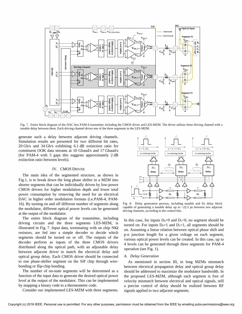
Fig.1, is to break down the long phase shifter in a MZM into shorter segments that can be individually driven by low-power CMOS drivers for higher modulation depth and lower total power consumption by removing the need for an electrical DAC in higher order modulation formats (i.e.PAM-4, PAM-16). By turning on and off different number of segments along the modulator, different optical power levels can be generated at the output of the modulator.
The entire block diagram of the transmitter, including driving circuits and the three segments LES-MZM, is illustrated in Fig. 7. Input data, terminating with on chip 50Ω resistors, are fed into a simple decoder to decide which segments should be turned on or off. The outputs of the decoder perform as inputs of the three CMOS drivers distributed along the optical path, with an adjustable delay between adjacent driver to match the electrical delay and optical group delay. Each CMOS driver should be connected to one phase-shifter segment on the SiP chip through wire-bonding or flip-chip bonding.
The number of on-state segments will be determined as a function of the input data to generate the desired optical power level at the output of the modulator. This can be implemented by mapping a binary code to a thermometer code.
Consider our implemented LES-MZM with three segments.
In this case, for inputs D0=0 and D1=0, no segment should be turned on. For inputs D0=1 and D1=1, all segments should be on. Assuming a linear relation between optical phase shift and p-n junction length for a given voltage on each segment, various optical power levels can be created. In this case, up to 4 levels can be generated through three segments for PAM-4 operation (see Fig. 1).
A. Delay Generation As mentioned in section III, in long MZMs mismatch
between electrical propagation delay and optical group delay should be addressed to maximize the modulator bandwidth. In the proposed LES-MZM, although each segment is free of velocity mismatch between electrical and optical signals, still a precise control of delay should be realized between RF signals applied to two adjacent segments.
Lb
CpE CpO
Vbias
Lb
CpE CpO
Vbias
Segment #1
Lb
CpE CpO
VbiasVDD_H
Data
QQ rdamp
Clk
D1 D0
Decoder
S0
S0
S1
S1
S2
S2
b1
b2
Vin_H
Vin_L
VDD_HVDD_L
CM
L to
CM
OS
Differential to
Single ended
Level shifter
VDD_L
VDD_H
VDD_L
VDD_L
0
Segment #3
Segment #2
Optical InputEIC PIC
VDD_Delay Blocks
Cj
Rs
Cj
Rs
Out
put
Stag
e
VDD_H
Data
QQ rdamp
Clk
Vin_H
Vin_L
CM
L to
CM
OS
Differential to
Single ended
Level shifter
VDD_L
Out
put
Stag
e
VDD_H
Data
QQ rdamp
Clk
Vin_H
Vin_L
CM
L to
CM
OS
Differential to
Single ended
Level shifter
VDD_L
Out
put
Stag
e
Optical path
Electrical path
Delay netw
ork
b0 CLK
Driving Channel
Fig. 7. Entire block diagram of the DAC less PAM-4 transmitter including the CMOS driver and LES-MZM. The driver utilizes three driving channel with a tunable delay between them. Each driving channel drives one of the three segments in the LES-MZM.
t0
T
t1 = t0 +Δτ1
T
t2 = t0 +τ+Δτ2
T
t3 = t0 +2τ+Δτ3
T
τ + (Δτ2-Δτ1)
CLK TL
τ
Delay
Δτ1
TL
τ
Delay
Δτ2 Delay
Δτ3 τ + (Δτ3-Δτ2)
ΔtΔt
to retiming latche to retiming latche to retiming latche
b0b1b2
Fig. 8. Delay generation process, including tunable and fix delay block capable of generating a tunable delay up to ~22.5 ps between two adjacent driving channels, according to the control bits.
Copyright (c) 2016 IEEE. Personal use is permitted. For any other purposes, permission must be obtained from the IEEE by emailing [email protected]

1) Delay Network The clock input is fed into each driving channel after
passing through a delay network whose block diagram is shown in Fig. 8. It comprises three delay blocks (i.e., ∆τ1, ∆τ2 and ∆τ3) to generate the desired delays for respective driving channels. This delay network is based on the difference between the delays generated in two adjacent delay blocks, enabling precise delay control between two adjacent segments. This approach is more tolerant to variations than delay generation schemes using absolute delays.
The delay control is illustrated in Fig. 9a. For the first delay block, only a fixed delay of 10 ps (∆τ1) is implemented for the purpose of differential delay control. The second delay block (∆τ2) consists of a coarse delay and a fine delay, both of which are tunable. The coarse delay is controlled by the control bit, b0, switching between 17.5 ps and 27.5 ps. The fine delay adjustment is implemented by means of the control bits b1, b2 with a tuning step of 2.5 ps. Similarly, ∆τ3 consists of a coarse delay of either 25 ps or 45 ps and a fine delay adjustable with a step of 5 ps (see Fig. 9a).
As illustrated in Fig. 8, assume the input clock signal is fed in at t0. Taking into account the delay blocks and the transmission lines (TLs) between them, the clock signals arrive at the re-timing latches at times:
t1 = t0 + ∆τ1 = t0 + 10 ps
t2 = t0 + τ + ∆τ2 = t0 + τ + coarse delay + (k × 2.5) ps t3 = t0 + 2τ + ∆τ3 = t0 + 2τ + coarse delay + (k × 5) ps
(2)
where k ∈ (0,1,2,3) is the number of fine tuning steps. Hence, the generated delay between two adjacent driving channels is ∆t = (ti-ti-1) = τ + (10 × b0) + k × 2.5 ps. This delay does not depend on the absolute value of the delay generated in each delay block. The minimum and maximum of the total delay between two adjacent channels are 5 ps and 22.5 ps, respectively. 2) Fixed and Tunable Delay Elements
Each delay block has a fixed delay (τ) from a single-wire shielded TL implemented on a thick metal layer for low RF losses. The cross section of the TL is shown in Fig. 9b.
The tunable delays (∆τ2, ∆τ3) are achieved by an inverter-based structure, as shown in Fig. 10a. The parasitic capacitance limits the bandwidth of the inverter. An inductively enhanced design is adopted to improve the bandwidth, where an inductor (Ls) is used to compensate for the effects of the unwanted capacitor from the inverter and the buffer stage after the inverter.
Delay between input and output nodes of the inverter is controlled by changing the current passing through the inverter by means of b0 for the coarse delays (17.5 ps and 27.5 ps in ∆τ2, 25 ps and 45 ps in ∆τ3). The fine delay element, as shown in Fig. 10b, needs two inputs. One input (clk2), which is connected to the output of the coarse delay, is delayed compared to the other input (clk1, i.e., the same input of the coarse delay) to generate the output clocks according to b1, b2 that control the tail currents. The fine delay adjustment is realized by changing the ratio of the currents (I1 and I2)
passing through the two branches of the differential pair.
B. Driving Channel A block diagram of each driving channel is given in Fig. 7.
The clock and driving signals (Si, S i, i=0,1,2) are applied to a high speed current mode logic (CML) latch for re-timing. Driving signals are applied to the driving channels as functions of input digital data (D0, D1) after certain delays as discussed above. 1) CML Latches:
Figure 11 shows a circuit schematic of the CML latch. Generally, a CML latch consists of two main sub-circuits: an input tracking circuit (shaped by M3 and M4) and a cross coupled regenerative pair in output (Mf1, Mf2). When VCLK is in the “high” state, the input voltage is tracked by the input differential pair, while M6 is blocking the current passing through the cross coupled regenerative pair in the output. When VCLK is in the “low” state, the cross-coupled regenerative pair stores the tracked voltage at the output load capacitance.
There are three criteria that must be considered in designing a CML latch: output voltage swing, voltage gain of the input differential pair, and bandwidth. The maximum allowable differential output voltage swing in a CML latch can be expressed by 2×rd1×ID, M1. As explained in [21], output voltage swing is limited by the threshold voltage of the NMOS devices in Fig. 11.
M8
M7via
10ps
20ps
Δτ2
Δτ3
10ps
Δτ1
12.5
ps
15ps
17.5
ps
22.5
ps
25ps
27.5
ps
10ps
30ps
b1, b2
15ps
20ps
25ps
35ps
40ps
45ps
b0=0
b0=1
b0=0
b0=1
(a) (b)
Fig. 9. (a) Delay generation in ∆τ1 and ∆τ2 with the control bits. One bit is assigned to the coarse delay and two others choses one of the fine delays. The maximum and minimum of the total delay between two adjacent channels is 5 ps and 22.5 ps (including the 5ps from transmission line). (b) Cross section of the transmission line for the fixed delay. The width of the signal path is chosen to be 4 µm while its length is 600 µm to generate 5ps fix delay.
InOut
rs1
Mn1
i1 i2
a
rs2
Ls1 Ls2
clk1 clk2
clk OutMp1
Mn2 M1 M2 M3 M4
I1 I2
b0
b1, b2
(a) (b) Fig. 10. (a) Tunable coarse-delay element capable of generating two delays, 17.5 ps and 27.5 ps in ∆τ1, 25 ps and 45 ps in ∆τ2. (b) Tunable fine delay element, mixing two clocks in different portions according to the tail current in each branch, to generate the output clock.
Copyright (c) 2016 IEEE. Personal use is permitted. For any other purposes, permission must be obtained from the IEEE by emailing [email protected]
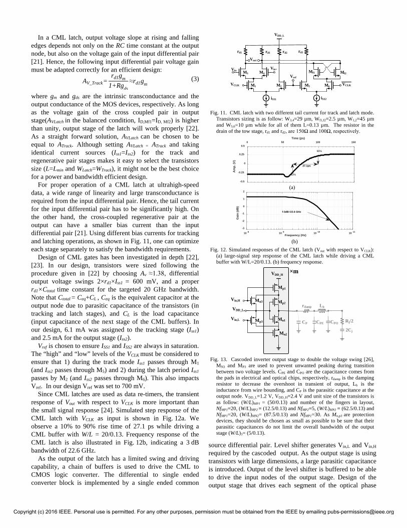
In a CML latch, output voltage slope at rising and falling edges depends not only on the RC time constant at the output node, but also on the voltage gain of the input differential pair [21]. Hence, the following input differential pair voltage gain must be adapted correctly for an efficient design:
AV_Track=rd1gm
1+Rgds≈rd1gm (3)
where gm and gds are the intrinsic transconductance and the output conductance of the MOS devices, respectively. As long as the voltage gain of the cross coupled pair in output stage(AVLatch in the balanced condition, ID,Mf1=ID, Mf2) is higher than unity, output stage of the latch will work properly [22]. As a straight forward solution, AVLatch can be chosen to be equal to ATrack. Although setting AVLatch = ATrack and taking identical current sources (Iss1=Iss2) for the track and regenerative pair stages makes it easy to select the transistors size (L=Lmin and WLatch=WTrack), it might not be the best choice for a power and bandwidth efficient design.
For proper operation of a CML latch at ultrahigh-speed data, a wide range of linearity and large transconductance is required from the input differential pair. Hence, the tail current for the input differential pair has to be significantly high. On the other hand, the cross-coupled regenerative pair at the output can have a smaller bias current than the input differential pair [21]. Using different bias currents for tracking and latching operations, as shown in Fig. 11, one can optimize each stage separately to satisfy the bandwidth requirements.
Design of CML gates has been investigated in depth [22], [23]. In our design, transistors were sized following the procedure given in [22] by choosing Av ≈1.38, differential output voltage swings 2×rd1×Iss1 = 600 mV, and a proper rd1×Ctotal time constant for the targeted 20 GHz bandwidth. Note that Ctotal = Ceq+CL , Ceq is the equivalent capacitor at the output node due to parasitic capacitance of the transistors (in tracking and latch stages), and CL is the load capacitance (input capacitance of the next stage of the CML buffers). In our design, 6.1 mA was assigned to the tracking stage (Iss1) and 2.5 mA for the output stage (Iss2).
Vref is chosen to ensure ISS1 and ISS2 are always in saturation. The “high” and “low” levels of the VCLK must be considered to ensure that 1) during the track mode Iss1 passes through M1
(and Iss2 passes through M5) and 2) during the latch period Iss1 passes by M2 (and Iss2 passes through M6). This also impacts Vref. In our design Vref was set to 700 mV.
Since CML latches are used as data re-timers, the transient response of Vout with respect to VCLK is more important than the small signal response [24]. Simulated step response of the CML latch with VCLK as input is shown in Fig. 12a. We observe a 10% to 90% rise time of 27.1 ps while driving a CML buffer with W/L = 20/0.13. Frequency response of the CML latch is also illustrated in Fig. 12b, indicating a 3 dB bandwidth of 22.6 GHz.
As the output of the latch has a limited swing and driving capability, a chain of buffers is used to drive the CML to CMOS logic converter. The differential to single ended converter block is implemented by a single ended common
source differential pair. Level shifter generates Vin,L and Vin,H required by the cascoded output. As the output stage is using transistors with large dimensions, a large parasitic capacitance is introduced. Output of the level shifter is buffered to be able to drive the input nodes of the output stage. Design of the output stage that drives each segment of the optical phase
VDD_L
Vref
Vin+Vin-
VCLK VCLK
Vout
iSS1 iSS2
rd1 rd1 rd2 rd2
M1 M2
M3 M4
M5 M6
Mf1 Mf2
Fig. 11. CML latch with two different tail current for track and latch mode.
Transistors sizing is as follow: W3,4=29 µm, Wf1,f2=2.5 µm, W1,2=45 µm and W5,6=10 µm while for all of them L=0.13 µm. The resistor in the drain of the tow stage, rd1 and rd2, are 150Ω and 100Ω, respectively.
(a)
(b) Fig. 12. Simulated responses of the CML latch (Vout with respect to VCLK):
(a) large-signal step response of the CML latch while driving a CML buffer with W/L=20/0.13. (b) frequency response.
×m
CPE
VDD_H
Vin,H
Vin,L
VDD_L
Mp1
Mp2
Mn1
Mn2
Mp3
Mn3
CP
Lb
CPO Rj/2
2Cj
rdamp
Fig. 13. Cascoded inverter output stage to double the voltage swing [26],
MN3 and MP3 are used to prevent unwanted peaking during transition between two voltage levels. CPE and CPO are the capacitance comes from the pads in electrical and optical chips, respectively, rdamp is the damping resistor to decrease the overshoot in transient of output, Lb is the inductance from wire bounding, and CP is the parasitic capacitance at the output node. VDD_L=1.2 V, VDD_H=2.4 V and unit size of the transistors is as follow: (W/L)MP1 = (50/0.13) and number of the fingers in layout, NfMP1=20, (W/L)MP2 = (12.5/0.13) and NfMP2=5, (W/L)MN1 = (62.5/0.13) and NfMP1=20, (W/L)MN2= (87.5/0.13) and NfMP1=30. As Mn,p3 are protection devices, they should be chosen as small as possible to be sure that their parasitic capacitances do not limit the overall bandwidth of the output stage (W/L)3= (5/0.13).
0 50 100 150Time (ps)
-0.5
-0.25
0
0.25
0.5
Am
p. (V
)
10%
90%
27.1ps
10 8 10 9 10 10 10 11Frequency (Hz)
-3
-2
-1
0
1
2
Gai
n (d
B)
f-3dB=22.6 GHz
Copyright (c) 2016 IEEE. Personal use is permitted. For any other purposes, permission must be obtained from the IEEE by emailing [email protected]

shifter is presented in continue. 2) Output Stage:
Simulation results in Fig. 6 were obtained by applying a 2Vp-p electrical signal to drive each segment. Considering the limited voltage head room in submicron CMOS process, a cascoded configuration (Fig. 13) is adopted in order to achieve the required voltage swing, which is widely used for optical modulators [25], [26]. The cascoded output stage used here needs two inputs voltage levels (see Fig. 13):
1.2V ≤ Vin,H ≤ 2.4V and 0V ≤ Vin,L≤ 1.2V (4)
applying this approach, the output swing can be doubled from VDD to 2VDD without over-stressing the NMOS and PMOS devices in the output stage.
The load capacitance at the output node of the driver, CLoad,
includes the pn-junction capacitance (Cj) of the optical phase shifter and the parasitic capacitances from the output stage
CLoad =2Cj+Cgd+Cdb (5)
where Cgd is the total capacitance between the gate and drain terminals and Cdb is the total capacitance between the drain and body terminals of MN1, MP2. The transistors in the output stage have to be sized according to the slew rate requirement for the desired data rate. For a 20 Gbaud transmitter, a slew-rate limited driver ideally must present a rise and fall time of no more than 17.5 ps. The required current to charge CLoad by Vdrive is:
ID= JD. W ≥ CLoadVdrive
tr (6)
where JD is the transistor current density and W is the width of the transistor.
According to(5) and assuming Vdrive = 2V and tr =17.5 ps, the required current is calculated to be 35 mA. Transistors in the output stage have to be sized to supply this high current, while offering the highest possible bandwidth. This means that transistors must be sized for the current density at the peak fT in the CMOS process used (≈ 0.127 mA/µm in our case) [27].
V. RESULTS OF THE CO-SIMULATION The optical transmitter is simulated following the procedure
illustrated in Fig. 2. Two 20 Gb/s, 215-1 PRBS bit patterns (where skewed with respect to each other for decorrelation) are fed to the designed CMOS driver. The equivalent circuit elements extracted from the optical phase shifter simulation are used as the load in the CMOS driver model developed in Section IV. The output of a single driving channel for different multiplicity factors is shown in Fig. 14, multiplicity factor m = 4 is chosen in our design to achieve the required voltage swing (Fig. 14, eye diagram with darkest line). Although the value of rise/fall time is far from its ideal value for a slew-rate limited driver, we still observe a clear eye at 20 Gbaud for 2 Vp-p swing in Fig. 14. This output stage is driven with two input signals, both with a full swing of VDD, so the output stage does not have to offer a high value of gain to its inputs.
Simulated output waveforms of the CMOS driver are input to the optical model developed in Section III for the three-segment LES-MZM. Simulated results of the optical
transmitter for two bitrates, 20 Gb/s and 37 Gb/s, are shown in Fig. 15. Compared to the results shown in Fig. 6 (where input electrical signals are ideal square waves with a 2.2Vp-p swing), the results of the co-simulation clearly show the effect of the bandwidth limitation from the driver on the output optical eye. It should be mentioned that during these simulations, the electrical signals and the photo detector are considered to be free of noise.
Eye opening in Fig. 15 is asymmetric (low levels are less separated than higher levels, same as the results in Fig. 6) due to the nonlinear relation between the length of the phase
Fig. 14. Performance of the driving channel loaded by the equivalent lumped
element circuit of one optical segment. Output eye diagrams for different values of multiplicity factor (m) in the output stage transistors.
100 ps
6.1d
B
(a)
60 ps
6.1d
B
(b)
Fig. 15 Co-simulation results for a three segments LES-MZM. a) at 20 Gb/s, b) at 34 Gb/s. A 14 ps delay is set between the adjacent driving channels.
Fig. 16. Effect of failure in maintaining the required delay (14 ps) between
driving channels on the output optical eye at 30 Gb/s. Center point of the middle eye opening is skewed from its ideal point. Delay between two adjacent channel, ∆t, is set to be 10ps, that is 4ps less than the required 14 ps delay.
(a) (b) Fig. 17 (a) CMOS driver, (b) CMOS driver wire bounded to SiP LES-MZM.
0 10 20 30 40 50 60 70 80 90 100
Time (ps)
-0.5
0
0.5
1
1.5
2
2.5
Am
plitu
de
m=4
m=2
m=1
Copyright (c) 2016 IEEE. Personal use is permitted. For any other purposes, permission must be obtained from the IEEE by emailing [email protected]
shifter and optical power at the output. Hence a compensation technique could be used to equalize the eyes, by manipulating the phase shifter length in each segment.
Proper delay generation between two adjacent driving channels affects the performance of transmitter. In Fig. 16, imperfection in the output optical eye due to failure in obtaining the required delay between two adjacent segment is shown. Skewed eye opening severely affects the BER performance of the transmitter, especially at higher baud rates where the bit duration is shorter.
VI. MEASUREMENT AND DISCUSSION The CMOS driver is fabricated in IBM 130 nm RF process. The entire die area of the driver is 1.5mm2 (1 mm×1.5 mm). The photonic chip was fabricated at A*STAR's IME, Singapore. A photo of the LES-MZM and its co-designed CMOS driver is shown in Fig. 17. Wire bonding is used to connect the output of each channel in the CMOS driver to each segment of the MZM. The operating point of the MZM is adjusted by means of DC bias voltage to achieve maximum eye opening (as a result, the bias point is slightly shifted from the quadrature point of the modulator).
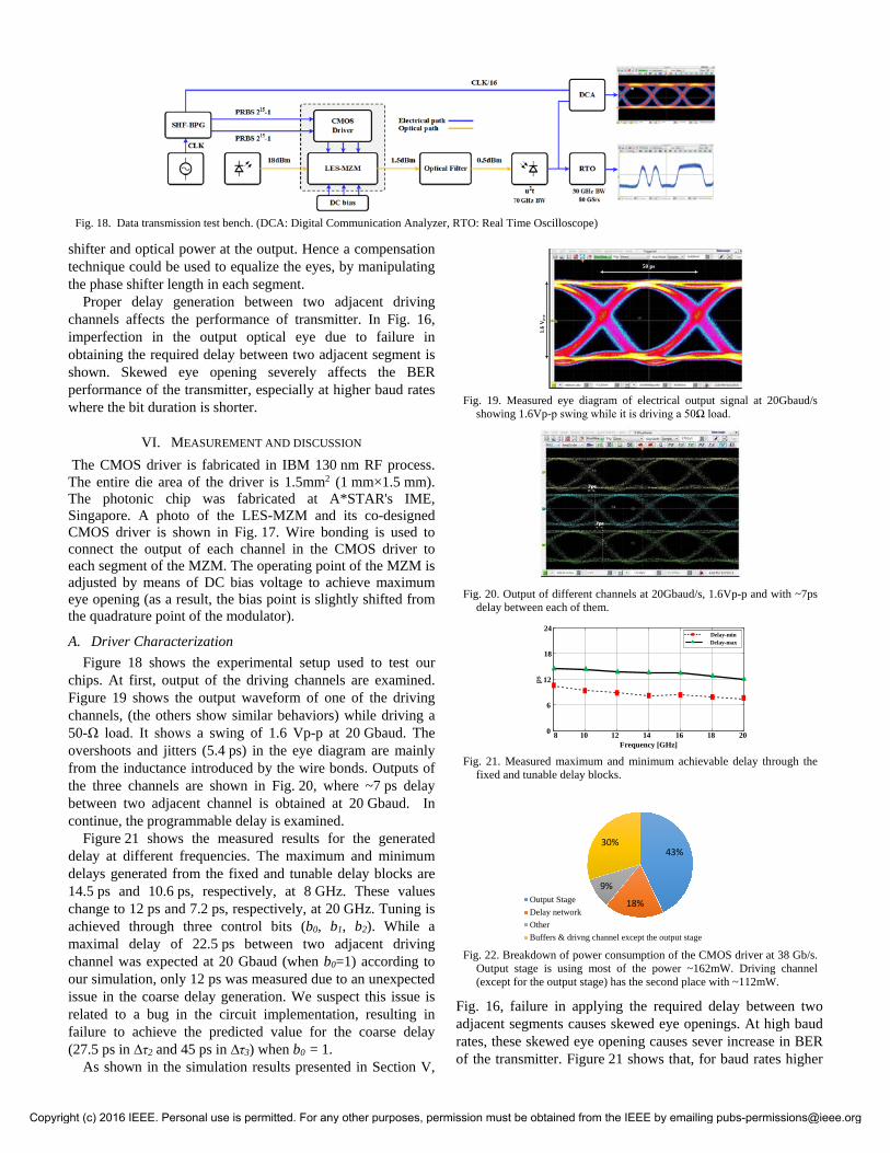
A. Driver Characterization Figure 18 shows the experimental setup used to test our
chips. At first, output of the driving channels are examined. Figure 19 shows the output waveform of one of the driving channels, (the others show similar behaviors) while driving a 50-Ω load. It shows a swing of 1.6 Vp-p at 20 Gbaud. The overshoots and jitters (5.4 ps) in the eye diagram are mainly from the inductance introduced by the wire bonds. Outputs of the three channels are shown in Fig. 20, where ~7 ps delay between two adjacent channel is obtained at 20 Gbaud. In continue, the programmable delay is examined.
Figure 21 shows the measured results for the generated delay at different frequencies. The maximum and minimum delays generated from the fixed and tunable delay blocks are 14.5 ps and 10.6 ps, respectively, at 8 GHz. These values change to 12 ps and 7.2 ps, respectively, at 20 GHz. Tuning is achieved through three control bits (b0, b1, b2). While a maximal delay of 22.5 ps between two adjacent driving channel was expected at 20 Gbaud (when b0=1) according to our simulation, only 12 ps was measured due to an unexpected issue in the coarse delay generation. We suspect this issue is related to a bug in the circuit implementation, resulting in failure to achieve the predicted value for the coarse delay (27.5 ps in ∆τ2 and 45 ps in ∆τ3) when b0 = 1.
As shown in the simulation results presented in Section V,
Fig. 16, failure in applying the required delay between two adjacent segments causes skewed eye openings. At high baud rates, these skewed eye opening causes sever increase in BER of the transmitter. Figure 21 shows that, for baud rates higher
Fig. 18. Data transmission test bench. (DCA: Digital Communication Analyzer, RTO: Real Time Oscilloscope)
50 ps
1.6
Vp-
p
Fig. 19. Measured eye diagram of electrical output signal at 20Gbaud/s
showing 1.6Vp-p swing while it is driving a 50Ω load.
Fig. 20. Output of different channels at 20Gbaud/s, 1.6Vp-p and with ~7ps
delay between each of them.
8 10 12 14 16 18 200
6
12
18
24
ps
Delay-minDelay-max
Frequency [GHz] Fig. 21. Measured maximum and minimum achievable delay through the
fixed and tunable delay blocks.
Fig. 22. Breakdown of power consumption of the CMOS driver at 38 Gb/s.
Output stage is using most of the power ~162mW. Driving channel (except for the output stage) has the second place with ~112mW.
43%
18%
9%
30%
Output StageDelay networkOtherBuffers & drivng channel except the output stage
Copyright (c) 2016 IEEE. Personal use is permitted. For any other purposes, permission must be obtained from the IEEE by emailing [email protected]

than 17 GHz, the maximum delay achieved is less than 13 ps, smaller than the optimal value (14 ps) predicted by simulation.
Total power consumption of the driver was 375 mW for 38 Gb/s. The breakdown of power consumption of the driver is shown in Fig. 22. The driver output stage consumers most of the power. CML buffers consume 30% of the total power. Power consumption decrease to 290 mW at 20 Gb/s.
B. Data Transmission The transmitter is driven directly by binary signals, i.e.,
without signal processing. Two length 215-1 binary sequences are generated by an SHF pattern generator; the bit rate is varied. The first signal (LSB) is fed to the first driving channel and the second signal (MSB) is split and fed to the second and third driving channels (based on the decision made by the decoder) to create a PAM-4 signal.
At the receiver side, the PAM signal is photodetected (by a u2t Photonics A.G. photo-detector with 70 GHz bandwidth), and captured using a 30 GHz real time oscilloscope (RTO) with sampling rate of 80 GSample/s. Also the optical eye diagrams are captured by means of a Digital Communication Analyzer (DCA). Output optical eye diagram for two different bitrates (20 Gb/s and 34 Gb/s) are presented in Fig. 23. Although for 34 Gb/s eye diagram shows very close eye opening in each level of PAM-4, at 20 Gb/s the eye opening in PAM-4 levels are very clean and suggest a transmission with a very low BER.
Offline DSP starts with a super Gaussian 4th order low pass filter and bandwidth set to the PAM main transmission lobe
for each bit rate. Three different post compensation methods are examined: 1) no post compensation, 2) a minimum mean square error (MMSE) equalizer, and 3) a fractionally spaced MMSE (FS-MMSE) equalizer. For the first and second cases data is down sampled to one sample per symbol; for the FS-MMSE data is down sampled to 2 samples per bit period. Following a synchronization block, equalization is performed on a training sequence of length 1000 symbols, and BER is calculated.
Figure 24 shows bit error rate for bit rates from 28 Gb/s to 40 Gb/s for the three compensation methods. The results show that without equalization the maximum bit rate under forward error correction (FEC) threshold of BER=3.7×10⁻³ is 28 Gb/s. Using MMSE and FS-MMSE increases system capacity to 37 Gb/s and 39.5 Gb/s respectively. This FEC threshold [28] offers a good compromise between bit rate overhead of 7% and data correction to ~10-12 when used with two interleaved extended BCH (1020,988) codes.
The significant improvement in performance when using two sample per symbol FS-MMSE indicates that failure in the delay management (the limited maximum achievable delay, coming from the failure in the coarse delay generation) contributed significantly to the impaired PAM performance. Using a fractionally spaced equalizer with more samples per symbol did not improve performance, showing the jitter error is well bounded. We include FS-MMSE results to indicate the potential of the SiP/CMOS solution. Once timing mismatch between segments is properly controlled, a simple MMSE would be sufficient.
At bit rates less than 24 Gb/s, the BER was found experimentally to be less than 1×10⁻⁵
. Unfortunately, due to finite memory of the real-time oscilloscope, error free performance (BER order 10-12) cannot be tested. The clear and open eye diagram in Fig. 23a for 20 Gb/s suggests error free operation at this bit rate. We calculated error vector magnitude (EVM) of the experimental received PAM4 constellation and obtained 6.23% EVM when using optimal thresholds (found numerically for the asymmetric eyes). This EVM corresponds to an SNR of 24 dB, well beyond the requirement for error free operation.
VII. CONCLUSIONS In summary, a DAC-less SiP PAM-4 transmitter with a
CMOS driver has been achieved, using a segmented MZM in
100ps
310 µw
1190 µw
60 ps
315 µw
1185 µw
(a) (b)
Fig. 23. Output optical PAM-4 eye diagrams at (a) 20 Gb/s and (b) 34 Gb/s
Data rate (Gbit/s)28 30 32 34 36 38 40
BER
10-4
10-3
10-2
10-1
100without Equalizerwith MMSE Equalizerwith FS-MMSE Equalizer
FEC Threshold
Fig. 24. BER vs. data rate of PAM-4 with no equalizer, an MMSE
equalizer, and an FS-MMSE equalizer.
Copyright (c) 2016 IEEE. Personal use is permitted. For any other purposes, permission must be obtained from the IEEE by emailing [email protected]

the carrier-depletion mode with a lateral pn junction. Data transmission with bit error rate below 3.7×10⁻³ (with post-compensation) was achieved near 40 Gb/s with a driver power consumption of 9.8 pJ/bit. Based on EVM at 20 Gb/s (where the driver power consumption drops to 290 mW), error free operation is expected at this bitrate. Despite the higher unit-bit power consumption (14.5 pJ/bit at 20 Gb/s), lower baud rates eliminate the burden of DSP on the receiver side. Tradeoffs must be taken in real applications.
Our optical circuit model of the LES-MZM allows for efficient electrical and optical simulations of the PAM transmitter. Measured optical eye diagrams are in a fair agreement with the simulation results. According to simulation results, the bandwidth of the driver in 130 nm CMOS limits the performance of the optical transmitter, which can be improved by using more advanced CMOS processes. Delay management between the segments in the transmitter is a critical concern that should be addressed properly to benefit from the wide electro-optic bandwidth of the segmented MZMs.
Multi-segment transmitters can potentially remove the power consuming electrical DAC from optical links for low-cost applications. Most demonstrated DAC-less multi-level transmitters use either monolithic process [12] or vertical pn junctions [1], which are not widely available. Our results are achieved using commercially available CMOS and SiP processes, showing the efficacy of CMOS-SiP co-design and integration for low-power, high-speed multi-level transmitters.
REFERENCES [1] M. Mazzini et al., "25G Baud PAM-4 error free transmission over both
single mode fiber and multimode fiber in a QSFP form factor based on silicon photonics," in OFC, Los Angeles, CA, 2015, pp. 1-3.
[2] T. Takemoto et al., "A 25-Gb/s 2.2-W 65-nm CMOS Optical Transceiver Using a Power-Supply-Variation-Tolerant Analog Front End and Data-Format Conversion," in IEEE J Solid-st Circ., vol. 49, no. 2, pp. 471-485, Feb. 2014.
[3] H. Morita et al., "8.2 A 12×5 two-dimensional optical I/O array for 600Gb/s chip-to-chip interconnect in 65nm CMOS," in ISSCC Dig. Tech. Papers, San Francisco, CA, 2014, pp. 140-141.
[4] J. Proesel, C. Schow and A. Rylyakov, "25Gb/s 3.6pJ/b and 15Gb/s 1.37pJ/b VCSEL-based optical links in 90nm CMOS," in ISSCC Dig. Tech. Papers, San Francisco, CA, 2012, pp. 418-420.
[5] Y. Tsunoda et al., "22.8 A 24-to-35Gb/s x4 VCSEL driver IC with multi-rate reference less CDR in 0.13um SiGe BiCMOS," in ISSCC Dig. Tech. Papers, San Francisco, CA, 2015, pp. 414–415.
[6] X. Wu et al., "A 20Gb/s NRZ/PAM-4 1V transmitter in 40nm CMOS driving a Si-photonic modulator in 0.13µm CMOS," in ISSCC Dig. Tech. Papers, San Francisco, CA, 2013, pp. 128-130.
[7] P. Dong, C. Xie, L Chen, LL Buhl, and YK Chen, “112-Gb/s monolithic PDM-QPSK modulator in silicon,” in Opt. Express, vol. 20, pp. 624-629, 2012.
[8] M. Chagnon, M. Osman, M. Poulin, C. Latrasse, J.-F. Gagné, Y. Painchaud, C. Paquet, S. Lessard, and D. Plant, “Experimental study of 112Gb/s short reach transmission employing PAM formats and SiP intensity modulator at 1.3μm,” in Opt. Express, vol. 22, no. 17, p. 21018- 21036, 2014.
[9] D. Patel, A. Samani, V. Veerasubramanian, S. Ghosh, and D. Plant, “Silicon Photonic Segmented Modulator-Based Electro-Optic DAC for 100Gb/s PAM-4 Generation,” IEEE Photonic Tech. L, vol. 27, no. 23, pp. 2433–2436, 2015.
[10] R. Dubé-Demers, S. LaRochelle and W. Shi, "Ultra-Fast Pulse-Amplitude Modulation with a Femtojoule Silicon Photonic Modulator,” Optica, pp. 622-627, 2016.
[11] M. Webster, K. Lakshmikumar, C. Appel, C. Muzio, B. Dama and K. Shastri, "Low-power MOS-capacitor based silicon photonic modulators and CMOS drivers," in OFC, 2015, Los Angeles, CA, 2015, pp. 1-3.
[12] C. Xiong, D. Gill, J. Proesel, J. Orcutt, W. Haensch and W. M. J. Green, "A monolithic 56 Gb/s CMOS integrated nanophotonic PAM-4 transmitter," in IEEE OI, San Diego, CA, 2015, pp. 16-17.
[13] M. Cignoli et al., "22.9 A 1310nm 3D-integrated silicon photonics Mach-Zehnder-based transmitter with 275mW multistage CMOS driver achieving 6dB extinction ratio at 25Gb/s," in ISSCC Dig. Tech. Papers, San Francisco, CA, 2015, pp. 416–418.
[14] A. Samani, M. Chagnon, D. Patel, V. Veerasubramanian, S. Ghosh, M. Osman, Q. Zhong, and D. Plant, “A Low Voltage 35 GHz Silicon Photonic Modulator-Enabled 112 Gb/s Transmission System,” in IEEE Photonics J, vol. 7, no. 3, pp. 1–13, 2015.
[15] Lorenzo Pavesi, David J. Lockwood (Eds.), “Is Silicon Photonics a Competitive Technology to Enable Better and Highly Performing Networks?” in Silicon Photonics III Systems and Applications, Topics in Applied Physics, vol. 122, Heidelberg: Springer, 2016, ch. 16, pp. 447–472.
[16] T. Yamase, M. Sato, H. Noguchi, K. Sato and T. Kato, "Low-power multi-level modulation of InP MZM with in-line centipede structure directly driven by CMOS IC," in IEEE OECC/PS, Kyoto, 2013, pp. 1-2.
[17] A Shastri, C Muzio, M Webster, and G Jeans, "Ultra-Low-Power Single-Polarization QAM-16 Generation Without DAC Using a CMOS Photonics Based Segmented Modulator," in IEEE J Lightwave Tech., vol. 33, no. 6, pp. 1255-1260, March, 2015.
[18] H. Bahramiabrghouei; H. Sepehrian; C. Park; L. Rusch; W. Shi, "Time-Domain Large-Signal Modeling of Traveling-Wave Modulators on SOI," in IEEE J Lightwave Tech., vol. 34, no. 11, pp. 2812-2823, June, 2016.
[19] B. Milivojevic et al., "112Gb/s DP-QPSK transmission Over 2427km SSMF using small-size silicon photonic IQ modulator and low-power CMOS driver," in OFC/NFOEC, Anaheim, CA, 2013, pp. 1-3.
[20] https://www.lumerical.com [21] P. Heydari and R. Mohanavelu, "Design of ultrahigh-speed low-voltage
CMOS CML buffers and latches," in IEEE Transactions on Very Large Scale Integration (VLSI) Systems, vol. 12, no. 10, pp. 1081-1093, Oct. 2004.
[22] R. Nonis, E. Palumbo, P. Palestri and L. Selmi, "A Design Methodology for MOS Current-Mode Logic Frequency Dividers," in IEEE Transactions on Circuits and Systems I: Regular Papers, vol. 54, no. 2, pp. 245-254, Feb. 2007.
[23] M. Alioto and G. Palumbo, "Design strategies for source coupled logic gates," in IEEE Transactions on Circuits and Systems I: Fundamental Theory and Applications, vol. 50, no. 5, pp. 640-654, May 2003.
[24] J. Kim, J. K. Kim, B. J. Lee and D. K. Jeong, "Design Optimization of On-Chip Inductive Peaking Structures for 0.13- µm CMOS 40-Gb/s Transmitter Circuits," in IEEE Transactions on Circuits and Systems I: Regular Papers, vol. 56, no. 12, pp. 2544-2555, Dec. 2009.
[25] H. Li, Z. Xuan, A. Titriku, C. Li, K. Yu, B. Wang, A. Shafik, N. Qi, Y. Liu, R. Ding, T. Baehr-Jones, M. Fiorentino, M. Hochberg, S. Palermo, and P. Chiang, “A 25 Gb/s, 4.4 V-Swing, AC-Coupled Ring Modulator-Based WDM Transmitter with Wavelength Stabilization in 65 nm CMOS,” in IEEE J Solid-st Circ., vol. 50, no. 12, pp. 3145–3159, 2015.
[26] W. Bae, G. S. Jeong, Y. Kim, H. K. Chi and D. K. Jeong, "Design of Silicon Photonic Interconnect ICs in 65-nm CMOS Technology," in IEEE Transactions on Very Large Scale Integration (VLSI) Systems, vol. 24, no. 6, pp. 2234-2243, June 2016.
[27] J. F. Buckwalter, X. Zheng, G. Li, K. Raj and A. V. Krishnamoorthy, "A Monolithic 25-Gb/s Transceiver With Photonic Ring Modulators and Ge Detectors in a 130-nm CMOS SOI Process," in IEEE Journal of Solid-State Circuits, vol. 47, no. 6, pp. 1309-1322, June 2012.
[28] ITU-T Recommendation G.975.1, Appendix I.9 (2004).
Copyright (c) 2016 IEEE. Personal use is permitted. For any other purposes, permission must be obtained from the IEEE by emailing [email protected]