cmos/bicmos self-assembling and electrothermal ... · cmos/bicmos self-assembling and...
TRANSCRIPT

I
CMOS/BICMOS Self-assembling and Electrothermal Microactuators for Tunable Capacitors
by
Altug Oz
A thesis submitted in partial fulfillment of the requirements for the
degree of
Master of Science
in
Electrical and Computer Engineering
December, 2003
Department of Electrical and Computer Engineering Carnegie Mellon University
Pittsburgh, Pennsylvania, USA
Advisor: Dr. Gary K. Fedder
Second Reader: Dr. Tamal Mukherjee

Report Documentation Page Form ApprovedOMB No. 0704-0188
Public reporting burden for the collection of information is estimated to average 1 hour per response, including the time for reviewing instructions, searching existing data sources, gathering andmaintaining the data needed, and completing and reviewing the collection of information. Send comments regarding this burden estimate or any other aspect of this collection of information,including suggestions for reducing this burden, to Washington Headquarters Services, Directorate for Information Operations and Reports, 1215 Jefferson Davis Highway, Suite 1204, ArlingtonVA 22202-4302. Respondents should be aware that notwithstanding any other provision of law, no person shall be subject to a penalty for failing to comply with a collection of information if itdoes not display a currently valid OMB control number.
1. REPORT DATE DEC 2003 2. REPORT TYPE
3. DATES COVERED 00-00-2003 to 00-00-2003
4. TITLE AND SUBTITLE CMOS/BICMOS Self-assembling and Electrothermal Microactuators forTunable Capacitors
5a. CONTRACT NUMBER
5b. GRANT NUMBER
5c. PROGRAM ELEMENT NUMBER
6. AUTHOR(S) 5d. PROJECT NUMBER
5e. TASK NUMBER
5f. WORK UNIT NUMBER
7. PERFORMING ORGANIZATION NAME(S) AND ADDRESS(ES) Carnegie Mellon University,Department of Electrical and Computer Engineering,Pittsburgh,PA,15213-3890
8. PERFORMING ORGANIZATIONREPORT NUMBER
9. SPONSORING/MONITORING AGENCY NAME(S) AND ADDRESS(ES) 10. SPONSOR/MONITOR’S ACRONYM(S)
11. SPONSOR/MONITOR’S REPORT NUMBER(S)
12. DISTRIBUTION/AVAILABILITY STATEMENT Approved for public release; distribution unlimited
13. SUPPLEMENTARY NOTES
14. ABSTRACT see report
15. SUBJECT TERMS
16. SECURITY CLASSIFICATION OF: 17. LIMITATION OF ABSTRACT Same as
Report (SAR)
18. NUMBEROF PAGES
73
19a. NAME OFRESPONSIBLE PERSON
a. REPORT unclassified
b. ABSTRACT unclassified
c. THIS PAGE unclassified
Standard Form 298 (Rev. 8-98) Prescribed by ANSI Std Z39-18
II
Table of Contents
Abstract .............................................................................................................................................. iii
Chapter 1: Introduction ...................................................................................................................1
1.1 Motivation.......................................................................................................................................1
1.2 Previous Research ...........................................................................................................................2
1.2.1 Electrothermal Microactuators.............................................................................................2
1.2.2 RF MEMS Tunable Capacitors............................................................................................5
Chapter 2: Design and Modeling....................................................................................................9
2.1 Self-assembling / Electrothermal Actuators....................................................................................9
2.1.1 Basic Concepts of Self Assembly and CMOS Electrothermal Actuation............................9
2.1.2 Nanometer-scale Gap Closing Mechanism........................................................................12
2.1.3 Modeling of Micro-movers for Self-assembly and Electrothermal Actuation...................13
2.1.3.1 Simulations for the Displacement from Self-assembly........................................14
2.1.3.2 Simulations for the Displacement from Electrothermal Actuation ......................16
2.1.3.3 Analytical Modeling of Thermal Time Constants and Frequency Response.......16
2.1.4 Latch Mechanism for Low Power Operation.....................................................................19
2.1.4.1 Vertical Latch Mechanism ...................................................................................20
2.1.4.2 Lateral Latch Mechanism.....................................................................................21
2.2 RF MEMS Tunable Capacitors.....................................................................................................23
2.2.1 Gap & Area Tuning Topologies.........................................................................................24
2.2.1.1 Analytical Calculations for Tuning Ranges and Quality Factors.........................28
2.2.1.2 Simulations for Calculating Capacitance.............................................................36
2.2.2 Gap Tuning Topologies .....................................................................................................38
2.2.2.1 Analytical Calculations for Tuning Ranges and Quality Factors.........................38
2.2.2.2 Simulations for Calculating Capacitance.............................................................41
III
Chapter 3: Experimental Results .................................................................................................42
3.1 Characterization of Self-assembling and Electrothermal Actuators .............................................42
3.1.1 Lateral Displacement from Self-assembly .........................................................................42
3.1.2 Lateral Displacement from Electrothermal Actuation .......................................................45
3.1.3 Frequency Response and Thermal Time Constant.............................................................45
3.1.4 Nanometer Scale Gap Closing Mechanism........................................................................46
3.2 Characterization of RF MEMS Tunable Capacitors .....................................................................48
3.2.1 Gap & Area Tuning Topologies.........................................................................................48
3.2.2 Gap Tuning Topologies .....................................................................................................56
Chapter 4: Discussion and Conclusions ...............................................................................59
4.1 Discussion .....................................................................................................................................59
4.2 Conclusion ....................................................................................................................................61
Bibliography ......................................................................................................................................63
Appendix ............................................................................................................................................67
Acknowledgements ..........................................................................................................................69

IV
Abstract
Advanced RF systems on chip will benefit from microelectromechanical (MEMS) tunable
capacitors integrated on a CMOS or BICMOS chip with high quality factor (Q) and large tuning range.
RF circuits with on-chip CMOS/BICMOS MEMS tunable capacitors will have small footprints and will
not have the reduction in tuning range coming from fixed capacitance between off-chip circuit parts.
CMOS-MEMS micro-movers that use the principles of self-assembly and electrothermal actuation are
successfully designed, modeled, fabricated and characterized for use in RF tunable capacitors, latch
mechanisms and nanometer-scale gap-closing structures.
The micro-movers exploit the lateral stress gradient setup by embedding metal layers into
CMOS-MEMS beams that are offset from the centerline of the beam. Built-in residual stress in the
aluminum and silicon dioxide layers creates a gradient driving self-assembly upon microstructural
release. Electrothermal actuation generates a stress gradient from the different temperature coefficients of
expansion of the offset materials. This actuation has relatively low driving voltage of around 12 V
maximum, which is compatible with IC technology and silicon substrates.
Various micro-mover designs in four different CMOS/BICMOS processes are characterized. The
largest lateral displacement from self assembly is 11 µm in a 100 µm by 40 µm footprint. The largest
lateral displacement from electrothermal actuation is 25.5 µm in an actuator with the same footprint.
Frequency response of the micro-movers is limited by the thermal time constant with the fastest measured
3dB bandwidth of 178 Hz. The largest tuning range achieved among tunable capacitor designs is 352.4%
with a Q of 52 at 1.5 GHz.
For zero-power stand-by operation of RF MEMS capacitors, mechanical latch structures are
developed by sequencing micro-movers. Such mechanisms are also applied to assembly of lateral
nanometer-scale sidewall gaps for large capacitance and large electrostatic force per area. Mechanical
latch and nanometer-scale gap-closing mechanisms are successfully fabricated and tested.

1
Chapter 1. Introduction
Over the past decade, MEMS technology has been widely used in applications such as optical
communications, wireless systems, automotive sensors, aerospace systems, micro-robotics, chemical
sensors, biotechnologies, and micro probes. MEMS applications in the RF and microwave field have seen
an incredible growth in the past 12 years stemming from the superior high frequency performance of RF
MEMS switches. During these years, other RF and microwave MEMS devices have been designed such
as tunable capacitors, inductors, micro-machined transmission lines, micro-mechanical resonators and
filters. Design, modeling, fabrication and characterization of novel RF MEMS tunable capacitors and
their self-assembly and electrothermal actuation mechanisms that are integrated within CMOS / BICMOS
processes are described in this thesis.
1.1 Motivation
For wireless industries, there is a continuing demand for RF high performance transceivers with
lower-power, lower noise and smaller footprint. It is important to use high-quality factor (Q) passive
components such as inductors, tunable capacitors and switches in RF front-end circuits for low power and
low noise receivers. For oscillators and amplifiers, using a passive component with high-Q results in
better phase noise and power consumption. Quality factor of on-chip inductors and MOS varactors are
only the order of low 10s at higher frequencies, therefore off-chip passive components capable of higher
Q are widely used for RF front-end circuits. However, using an off-chip device increases the footprint of
the receiver. Recent MEMS-based passive components achieved Qs of 30-100 at several gigahertz
frequencies and have the potential to be used instead of the low-Q conventional on-chip passives. RF
front-ends with these micro-machined passives still have large footprints, because they employ two
separate die, one for micro-machined passives and one for electronics. On-chip MEMS passives are of
interest, if they can be demonstrated to achieve higher Qs and smaller footprints from the same design.
There is also an increasing demand for multi-band radio architectures, because of the need for
integration of different wireless systems with different operation frequencies. Tunable or reconfigurable

2
receiver components are required for these multi-band RF front-ends. Most of the on-chip varactors have
low tuning range (<3) and non-linear behavior. Over the past years, MEMS–based tunable capacitors also
achieved large tuning ranges (>8) [1] and linear behavior [2], but previous VCO designs with
micromechanical tunable capacitors have not achieved wide tuning for VCO application [3-6]. On-chip
interconnects introduce fixed capacitance to LC tank of the VCO, which decreases the tuning range
The goal for designing a novel MEMS tunable capacitor on a CMOS or BICMOS chip is to
achieve high Q and large tuning range and to use the capacitors with on-chip MEMS inductors [7] and
other electronics to design high performance front-end circuits. RF circuits with on-chip CMOS/BICMOS
MEMS tunable capacitors will have small footprints, and will not have the reduction in tuning range
coming from fixed capacitance between off-chip circuit parts. The top metal layer in the CMOS/BICMOS
process is used to define microstructures in the post-CMOS micromachining steps, eliminating the need
for any additional masks. For the actuation mechanism, electrothermal actuators are preferred for having
low driving voltages, which enables the compatibility with integrated circuits and silicon substrate. For
zero-power stand-by operation of RF MEMS capacitors, mechanical latch structures can be developed.
These types of capacitor designs enable reconfigurable RF filter and VCO applications. Another
important application of the microactuators and latch mechanisms is in assembling lateral nanometer-
scale sidewall gaps for large capacitance and large electrostatic force per area. Desirable gap sizes for
resonant filter applications range from about 50 nm or less to 500 nm. Conventional optical lithography
gap width in the CMOS microstructures is around 0.5 µm, which limits the performance of these devices.
1.2 Previous Research
1.2.1 Electrothermal Microactuators
Various micro-actuation techniques such as electrostatic, thermal, piezoelectric, or magnetic have
been demonstrated. Actuators based on electrostatic forces have been commonly used, due to their low
power and high frequency operation [8-9]. Although electrostatic actuators have these advantages, they
require high voltages (>40V) that are not compatible with most integrated circuit processes. The forces
produced by electrostatic actuators are in the range from 1µN to 10µN [8-9], which are lower than the

3
forces produced by other types of microactuators. Large areas are needed for electrostatic actuator
designs, which make system on-chip integration less feasible economically. Magnetic actuation uses the
force of attraction and repulsion between magnetic field produced by an electric current and a magnetic
material [10]. These types of actuators require extra fabrication steps. Piezoelectric actuators also have
similar problems with processing complexity, as they require piezo-electric materials modified by high
temperature steps [11]. On the other hand, devices based on electrothermal actuation can provide large
forces, large displacements, and low area consumption [12-28]. They can also operate in an integrated
circuit voltage regime (<5V). However, thermal actuators consume more power than electrostatic
actuators. Generally thermal actuators are slower than the electrostatic actuators. Usually thermal time
constants are longer than the electrical and mechanical time of constants. To alleviate this problem, the
thermal mass of the actuators should be designed as small as possible.
Some of the early electrothermal actuator designs are based on the bimorph effect, which relies
on the difference of thermal expansion coefficients between two adjacent layers on the device. By heating
these layers, a bending moment is created. However such actuators produce deflection in the direction
normal to the substrate [12]. One of the microactuator designs by Reithmuller and Benecke with 2.5 µm
thick locally deposited Au layer achieved 90µm displacement by using 200 mW power from 0.05mm2
area [12]. An electrothermal design by Sun and Carr uses the out of plane actuators to produce in-plane
deflections [13]. By using both electrothermal and electrostatic actuation at the same time, this actuator
design can produce 30 µm lateral deflection with 40mW power from 0.03 mm2 area [13]. Because of the
fact that processing adjacent bimorph materials is so complicated, the lateral actuation mechanism is very
difficult to achieve by using the bimorph approach. Judy et al. [14] developed an actuator, which achieved
in plane actuation by using serpentine shape actuators with complicated processing. One recent actuator
design by Oz and Fedder, which will be explained in the following chapter, uses the CMOS/BICMOS
interconnect stacks for laying the bimorph materials to make the processing easier and also achieved
lateral deflections [15]. This actuator demonstrated 3.5 µm deflection by using 18 mW power from 0.04
mm2 area [15]. Lateral “heatuator” microactuators are based on the asymmetrical thermal expansion of a

4
microstructure, which has two different cross sections and is processed in one structural layer [16-18].
The most recent design by Comtois, Michalicek and Baron can produce 20 µm deflection and 19 µN
force with 37 mW power from a small area (0.01 mm2) [18]. The 3-db bandwidth for this design is 7 kHz,
and maximum frequency for full deflection is 1.57 kHz [18]. For the beam-bent actuators, designed by
Gianchandani et al. [19] current is passed through the V-shaped beam anchored at two ends to cause a
thermal expansion at the center of the actuator. A fabricated single device can produce 5 µm displacement
and 8300 µN force with 180 mW from 0.01 mm2 area, and some cascaded ones demonstrated 3 µm
deflection and 132 µN force with 40 mW from 0.7 mm2area [20]. The trade-off between power-area and
force can be seen in these actuators. The measured -3dB bandwidth for both cascaded and single devices
is 700 Hz [20]. To increase the output displacements, rotary actuators and inchworm designs are
demonstrated by using multiple bent-beam thermal actuators orthogonally [21]. For rotary actuator
designs, the displacement is increased from 3 µm to 33µm, but the power is also increased from 40 mW
to 375 mW as multiple actuators are used. Zero-standby power is achieved by the inchworm designs,
which means that the power is only needed during the switching time, not for the on or off cases [21].
Sun, Farmer and Carr developed a similar zero-standby operation design by employing a mechanical latch
structure [22]. For near zero-power operation, a RF MEMS switch by Robert et al. [23] is designed by a
combination of thermal actuation and electrostatic latching. 400 mW of power is consumed for switching
operation, but only 10 V is needed for the electrostatic latch mechanism with close to zero continuous
power. The switching time for the electrothermal actuation is 200 µs.
There are several examples of applications in MEMS utilizing electrothermal actuators including:
RF MEMS tunable capacitors [4-6], RF MEMS switches [23], an optical fiber micro switch [24], rotary
micro-engines [21], micro-tweezers [25], and positioners [26]. There are also several efforts to model
electrothermal actuators, including the physics of temperature dependent material properties and Finite
Element Analysis (FEA) modeling techniques [27-28].

5
1.2.2 RF MEMS Tunable Capacitors
Complete receiver systems on a single chip require voltage-controlled oscillators (VCOs) with
gigahertz frequencies, and low phase noise and tunable RF filters with low insertion loss. Tunable
capacitors with high Q are desired in VCOs and RF filters for achieving better good performance. Micro-
mechanical high-Q tunable capacitors have been used for VCO [3-6] and RF filter applications [29].
Other than the MEMS-based tunable capacitors, several other strategies, which include the
implementation of MOS varactors or switched capacitor banks, have been used to achieve wide tuning
range. Distortion and linearity are the two main problems associated with these approaches. Compared
with solid-state varactors, MEMS tunable capacitors have advantages of lower loss, larger tuning range
and more linear tuning characteristics.
In the past few years, many tunable capacitors based on MEMS technology have been designed
[1-6, 29-40]. These capacitor designs can be classified into two categories according to their tuning
mechanism; one category is gap tuning, and the other one is area tuning. MEMS-based RF tunable
capacitors can also be classified according to their actuating mechanisms which are; electrostatic,
electrothermal, and piezo-electric.
Some of the early gap tuning designs have low tuning ranges, because of the parasitic
capacitances coming from interconnects [3]. The parallel-plate capacitor designs with electrostatic
actuators have a theoretical 50% tuning range limitation [3], because the electrodes snap after the gap
between them becomes 2/3 of the initial gap. The parallel-plate vertical gap device demonstrated by
Young and Boser, has a tuning range of 16% and quality factor of 60 at 1 GHz [3]. A VCO is
implemented at 714MHz operating frequency with 14 MHz tuning range and a phase noise of -107
dBc/Hz at 100-kHz offset [3]. A Modified parallel-plate RF tunable capacitor is designed to increase the
tuning range larger than 50% limit by using three parallel plates [4]. From a 4 pF capacitor design, a
tuning range of 87% with 4.4 V controlling voltage and Q of 15.4 at 1 GHz are achieved [30]. A VCO is
also demonstrated with 24 MHz tuning at 1.336GHz operating frequency and phase noise of -98.5
dBc/Hz at 100-kHz offset [30]. A parallel plate design by Zou et al. [31] used a novel electrode design to

6
achieve a tuning range larger than the 50% snap-in limit. For this design, larger gaps are used in the
electrostatic actuation mechanism, compared to the gaps between the electrodes of the capacitor [31].
Tuning range of 69% is achieved by using 17 V driving voltages [31]. Designs based on a cantilever
beam also achieve tuning ranges larger than 50% [32-33]. The initial design by Hung and Senturia has a
tuning range of 81.8% with 40V controlling voltage [32]. Later designs have Q of 4 at 3 GHz and large
tuning range of 354% with 40 V controlling voltage [33]. Parallel-plate capacitor designs using
electrothermal and piezo-electric actuation do not have the 50% tuning range limitation. A parallel-plate
capacitor by Feng et al. [34] based on thermal actuation has lower driving voltages around 7 V, compared
to the capacitor based on electrostatic actuation. It has also large tuning ranges of 270% and high-Q factor
of 300 at 10 GHz [34]. Yao et al. [35] developed a capacitor based on piezo-electric actuation that has a Q
factor of 210 at 1 GHz with a 6 V controlling voltage.
The area tuning RF MEMS capacitors are demonstrated to solve the snap-in tuning range
limitation, when electrostatic actuation is used [36-37]. Early devices achieve tuning range of 300% with
5 V controlling voltage. Interdigitated finger structures with 30 µm thickness are used for capacitor
electrodes and the electrostatic actuation mechanism [36]. Recent designs use thicker and longer finger
blocks to increase the tuning range and the quality factor. Tuning ratio of 8.4:1 with 8 V controlling
voltage and Q factor of 35 at 2 GHz is demonstrated by using 40 µm thick finger electrodes [1]. Having a
12 pF nominal capacitance value and Q-factor of 200 at 400 MHz enables UHF filter applications for
these capacitor designs. An UHF filter with tuning range of 225-400 MHz is developed with an insertion
loss of 6.2 dB and Q factor of 100 for the operating frequency ranges [29]. The most recent capacitor
design by Rockwell Science Center achieves a linear tuning characteristic by forming a completely
electrically isolated capacitor [2]. Two sets of electrostatic comb drive actuators in opposing directions
are used to achieve a linear tuning characteristic. Another area tuning design uses the idea that the
dielectric between the electrodes is moved laterally to achieve high-Q factors [37]. Using a dielectric that
has large dielectric constant enables high-Q factors, because the same device would have bigger
capacitance with the same resistance losses. Q factors of 291 at 1 GHz and tuning range of 7% with 10 V

7
controlling voltage is demonstrated [37]. The biggest issue of these MEMS devices is the use of
separately fabricated CMOS/BICMOS electronics. For VCO and RF filter designs, on-chip and off-chip
interconnects between separate dies introduce large fixed capacitance to the LC tank, which decreases the
tuning range.
In this thesis work, several CMOS-compatible micromechanical tunable capacitors are
demonstrated to solve this separate die problem [38-40]. These MEMS capacitors can be classified as on-
chip devices, and can be easily used with on-chip inductor and CMOS/BICMOS electronics to design
VCOs and RF filters. These RF filter and VCO designs have larger tuning range, due to lower
interconnect capacitance between the capacitor, inductor and electronics. They also have a smaller
footprint, since everything is on the same chip, which enables future system-on-chip designs.
Electrothermal actuation is chosen, for its lower driving voltage, which is compatible with IC technology
and silicon substrates.
Fabrication steps of these microactuators are similar to CMOS post-processing techniques [41].
Structures are made using the CMOS interconnect stack and released with a maskless CMOS
micromachining process. The high-aspect-ratio CMOS micromachining technology begins with a
conventional foundry CMOS process. Versions of these lateral actuators were fabricated using Austria
Microsystems (AMS) 0.6 µm CMOS, Agilent 0.5 µm CMOS and TSMC 0.35 µm CMOS, IBM SiGe6HP
0.25 µm BICMOS and Jazz 0.35 µm BICMOS processes. After the foundry fabrication, three dry-etch
steps, shown in Figure 1.1, are used to define and release the structure. Figure 1.1(a) shows the cross
section of the chip after regular CMOS fabrication. In the first step of post-CMOS processing (Figure
1.1(b)), dielectric layers are removed by an anisotropic CHF3/O2 reactive ion etch (RIE) with the top
metal layer acting as an etch resistant mask. After the sidewall of the microstructure is precisely defined,
silicon trenches around the device are micromachined into the substrate using a deep RIE step (Figure
1.1(c)). The final step is an isotropic SF6/O2 RIE used to etch away the bulk silicon and release the
structure (Figure 1.1(d)). Multi-layer conductors can be built in the composite structure, which enables
more flexible designs than homogeneous conducting structures. The undercut of silicon in the release step

8
(Figure 1.1(d)) requires the placement of sensing circuits to be at least 40 µm away from the
microstructures.
(a) (b) (c) (d) Figure 1.1. CMOS-MEMS process. (a) CMOS chip after fabrication, (b) anisotropic RIE removes dielectric layers, (c) anisotropic RIE removes substrate, (d) isotropic RIE undercuts silicon substrate.
The remainder of this thesis reports on the development of the tunable capacitors and the micro-
mover structures. The design and modeling of self-assembly structures, electrothermal actuators, and RF
tunable capacitors will be discussed in Chapter 2. The experimental results for different designs will be
given in Chapter 3. In Chapter 4, the results from design, modeling and experiments will be compared and
discussed.

9
Chapter 2. Design and modeling
There is an ever increasing need for accurate modeling of MEMS devices. Once an accurate
model is built for one device topology, the consumed time for design and optimization is reduced.
Building accurate models for design of micro-movers and tunable capacitors is an ultimate goal of the
present work. Recently, RF circuits like RF filters and VCOs can be designed by using these tunable
capacitors and micro-movers. Having accurate models for the MEMS devices helps the designers to
communicate between the device level and the circuit level and iterate between those two levels during
the design process.
The concepts of lateral self-assembling actuators, electrothermal actuators and latching
mechanisms made from these actuators will be presented in Section 2.1. Also covered in this section are
finite-element simulation results of electrothermal actuation and analytic modeling of the thermal and
mechanical response. In Section 2.2, various topologies for tunable capacitors made with the micro-
movers will be discussed in detail. Parallel-plate analytic models with geometric design parameters for
capacitance and quality factor are presented along with supporting finite-element simulation results.
2.1 Self-assembling / Electrothermal Actuators
CMOS/BICMOS-MEMS micro-movers are capable of providing large lateral displacements for
tuning capacitors, self-assembly of small gaps in CMOS/BICMOS processes, latching structures and
other applications where lateral micro-positioning on the order of 1 to 10 µm is desired. Principles of self-
assembly and electrothermal actuation are used in design of these micro-movers. The new ability is to
design from layout, and thereby tailor, the lateral stress gradients and gradients of temperature coefficient
of expansion into the actuation beams. This design capability represents an advancement over prior
methods of designing electrothermal actuators and micro-movers in that enables high displacement
magnitude with small geometry and independent setting of displacement and stiffness. Prior work
exploits differences only in axial expansion coupled with mechanical lever action to produce motion. The
fabrication approach has the further advantage of being compatible with CMOS and hybrid CMOS/SiGe

10
bipolar processes, which enables less resistive losses and less parasitic capacitance for RF MEMS tunable
passive applications.
2.1.1 Basic Concepts of Self Assembly and CMOS Electrothermal Actuation
Motion is induced in specific beams by designing a lateral stress gradient within beam flexures.
The lateral stress gradient arises from purposefully offsetting the lower metal layers with respect to the
top metal layer of a CMOS-MEMS beam. A similar offset idea was presented for use in a lateral
capacitive infrared sensor [42]. Of particular importance is the ability to tailor the lateral stress gradient,
and therefore lateral moment, as a function along the beam length. This ability to set an internal moment
along the beam arises from different offset and width of the embedded layers. The microstructures are
made from the CMOS interconnect stack using a maskless CMOS micromachining process, however
these beams could be made in alternate custom processes. For example, the micro-movers can also be
made in hybrid CMOS/SiGe bipolar processes. The CMOS-MEMS beams are made from metal layers
embedded within a dielectric (silicon oxide and silicon nitride). The offset layers do not have to be metal,
and do not have to be embedded in dielectric. However, this particular design technique is particularly
advantageous in CMOS-MEMS, since no special processing must be done to implement the designs.
The primary concept of the lateral actuator is illustrated in Figure 2.1. This particular design is a folded-
flexure to relieve axial residual stress, as shown in Figure 2.1(a). The metal layers inside the flexure
beams are offset to one side of the beam for half the beam length, and to the other side for the remaining
half of the length. This arrangement provides a lateral stress gradient in one direction for half of the
beams, then to the other direction for the other half. For many CMOS-MEMS processes, the residual
stress in the offset aluminum layers is tensile, while the residual stress in the surrounding silicon oxide
layers is compressive. Therefore, the aluminum contracts and the silicon oxide expands once freed to
move. Upon release, this tailoring of stress provides a self-actuating operation, where the beams move
into a “S” shape, as shown in Figure 2.1(b). This shape eliminates any moments at the ends of the beam,
and therefore maximizes lateral motion with no rotation. Some residual moment may exist at the ends of
the beam due to manufacturing variation along the beam, though this is small. The design methodology

11
for placement of the inner metal layers aims to set the beam moment so as to mimic bending from an
external actuating force concentrated at the central piston. Sub-0.5 micron CMOS processes generally
have lower residual stress in both the aluminum and silicon oxide layers. Some CMOS processes provide
aluminum layers with compressive residual stress. In all cases, efficient CMOS-MEMS electrothermal
Figure 2.1. Primary concept of the micro-mover in CMOS/BICMOS processes, (a) before micro-structural release, (b) after micro-structural release, (c) after actuation.
doffset
doffset is the distance between the width center of the lower metal layers and the width center of the top metal layer

12
actuators can be designed, once the behavior in a given process is characterized.
The stiffness of the flexure in Figure 2.1 can be modified independent of the deflection. The
particular design in Figure 2.1 employs 12 beams. Additional beams, ideally in a symmetric arrangement,
may be added to increase the stiffness. This is a great advantage over electrostatic micro-actuation
schemes. Electrothermal actuation can be applied to any designed actuator. The heating is implemented in
CMOS-MEMS by embedding a polysilicon resistor inside the beam. Current flowing through the resistor
generates the heating power. Motion is induced from the different Temperature Coefficient of Expansion
(TCE) of the metal offset layers and the rest of the beam material (silicon oxide). In the case of CMOS-
MEMS, the offset aluminum layers have a much larger TCE than the surrounding silicon oxide. When
heated, the side of the beam with the aluminum offset will expand relative to the other side. This effect
leads to the actuated lateral motion, as illustrated in Figure 2.1(c).
2.1.2 Nanometer-scale Gap Closing Mechanism
An application of the micro-movers is in assembling lateral nanometer-scale sidewall gaps for
large capacitance and large electrostatic force per area. Desirable gap sizes range from about 50 nm or
less to 500 nm. These nanometer-scale gaps are particularly useful for improving the performance of
high-frequency nanoresonator devices. Conventional optical lithography limits gap width in the CMOS
microstructures to around 0.5 µm. Smaller gaps have been made in some other micromachining
processes, for example by forming a thin sacrificial oxide layer between silicon or polysilicon electrodes.
In our assembly approach, the gap as drawn in layout is much larger than the final nanometer-scale
dimension, as shown in Figure 2.2. One electrode of the gap may be a nanoresonator, exemplified by the
fixed-fixed beam in Figure 2.2. The other electrode of the gap is connected to a micro-mover. The micro-
mover shifts the electrode in the direction to narrow the gap. A rigid limit stop sets the desired final gap
value. Since the limit stop edge and the beam edge face the same direction, any overetch or underetch in
the processing will not affect the gap dimension. Theoretically, the gap can be set to an arbitrarily small
value, however the practical minimum gap is determined by the surface roughness of the sidewalls,

13
estimated to be less than 50 nm. A self-assembly micro-mover is ideal for this application, requiring zero
power. However, some CMOS processes have such low residual stress gradients that making self-
assembly micro-movers is impractical. In these cases, an electrothermal micro-mover shifts the electrode
and closes the gap. To maintain the gap closure without expending continuous power in the micro-mover,
a self-aligning lateral latch mechanism can be included. The lateral latch mechanisms will be explained in
Section 2.1.4.2.
Figure 2.2. Nanometer scale gap closing mechanism by using self-assembly. . 2.1.3 Modeling of Micro-movers for Self-assembly and Electrothermal Actuation
Micro-mover designs were fabricated in several processes, including the AMS 0.6 µm CMOS
process, Agilent 0.5 µm CMOS process, TSMC 0.35 µm CMOS process, IBM SiGe 6HP 0.25 µm
BICMOS process and Jazz 0.35 µm BICMOS process. For the modeling of the micro-movers, designs in
Jazz 0.35 µm BICMOS process will be analyzed.

14
Displacement magnitudes of the lateral self-assembly and actuation are verified quantitatively by
finite element analysis (FEA), using Coventorware [43]. For FEA, a simulation temperature, Tset, is
calculated to model the lateral actuation magnitude upon release of the actuator.
dsimset TTTT ++−= 0 (2.1)
where, Tsim, is the simulator initial temperature, which is 273 K, and Td is the ambient
temperature. To denotes the characteristic temperature, defined as the temperature at which a beam with
embedded offset metal layers exhibits zero deflection relative to layout. Information about analytical
equations for temperature dependant residual stress gradients can be found in [44, 45]. Design parameters
for the micro-mover structure are shown in Figure 2.3(a) by using a half part of the micro-mover in
Figure 2.1. Lbeam is the beam length in the actuator, Wbeam1 is the beam width set by the top metal layer in
the actuator, Wbeam2 is the beam width for embedded lower metal layers in the actuator with lateral offset,
Lplate is the plate length in the actuator, Wplate is the plate width in the actuator, Nbeam is the number of
parallel beams in the actuator and doffset is the offset, which is shown in Figure 2.1. The thermal
coefficient of expansion (TCE) values, that are used in the simulations are 28.3 µ/K for metal layers and
0.4 µ/K for oxide layers.
2.1.3.1 Simulations for the Displacement from Self-assembly
To perform a simulation in Coventorware, the characteristic temperature for that type of actuator
must be known. This information can be measured from lateral curl of a simple beam test structure, by
determining the temperature at which the structure is completely straight. Figure 2.3(b) is a scanning
electron micrograph of test cantilever structure at room temperature. The verniers at the tip of the beam
aid in measuring lateral displacement. By using these verniers 0.1 µm resolution can be achieved. The
beam width and composition of embedded metal layers must be same as the beams to be used in the
actuator design. Characteristic temperatures for different types of beams are listed in Table-2.1. To
simulate the lateral displacement for the self assembly, these characteristic temperatures are entered into
(2.1), with Td equal to the room temperature (294 K). Figure 2.3(c) is a simulation result for lateral self-

15
(a) (b)
(c) (d)
Figure 2.3. (a) Design parameters for a micro-mover structure, (b) simple beam structure, which are used to measure characteristic temperature, (c) self-assembly lateral displacement magnitude for a micro-mover design in Jazz 0.35 µm BICMOS process, (d) lateral displacement of electrothermal actuation at 425 K temperature.
Wbeam2 Wbeam1
Wplate Lplate
Nbeam
Lbeam

16
the tip of the actuator is 12.4 µm. There are two other parameters, that can also affect the displacement
magnitude of the self-assembly: having or not having a field oxide layer underneath the lowest metal
layer and similarly having or not having vias between metal layers. The designs in Table-2.1 do not have
vias between metal layers or field oxide under the lowest metal. For Device#1A, device#8A and
device#4B from Table 2.1 the top metal layer is metal 3, and lower embedded metal layers are metal1 and
metal2.
2.1.3.2 Simulations for the Displacement from Electrothermal Actuation
Figure 2.3(d) is a simulation result for lateral displacement from electrothermal actuation at
425 K for device#1A. From Figure 2.3(d), the electrothermal lateral displacement at the tip of the actuator
is -8.06 µm. Electrothermal displacement values may be defined alternatively as the displacement
difference relative to the self-assembly position at ambient temperature. For the electrothermal actuation
in Figure 2.3(d), the total displacement is then 12.4 µm + 8.06 µm = 20.46 µm. Simulated electrothermal
lateral displacements of two different actuator designs at different ambient temperatures (325 K, 350 K,
375 K, 400 K, 425 K, 450 K) are given in Table-2.2. The designs in Table-2.2 do not have vias between
metal layers or field oxide under the lowest metal.
2.1.3.3 Analytical Modeling of Thermal Time Constants and Frequency Response
Thermal Time Constant
The thermal time constant of the device is the total effective heat capacitance divided by the
thermal conductance of the device to substrate. The thermal time constant of the device can be modeled to
first order using the thermal equivalent circuit shown in Figure 2.4(a).
The thermal conductance, G, in the equivalent circuit is the sum of the heat conductance, Gact ,
through the actuator structure and then to the substrate, and heat conductance, Gair , through air to the
substrate. In calculating the thermal capacity, C, an assumption is made that the total thermal capacity of
beams and plates is lumped in the moving center plate.

17
(a) (b) Figure 2.4. (a) Thermal equivalent circuit for the microactuator for calculations of thermal time constant, (b) Model for calculation of mechanical resonance frequency.
Table 2.1. Lateral displacement from self-assembly for three different micro-mover designs in Jazz 0.35 µm BICMOS process, with their design parameter information.
Table 2.2. Lateral displacement from electrothermal actuation for two different micro-mover designs in Jazz 0.35 µm BICMOS process at different temperatures, with their design parameter information.
Lateral electrothermal actuation Device Number
Lbeam Wbeam1 Wbeam2 Lplate Wplate Nbeam Temperature of the actuator
Lateral displacement
325 K 4.3 µm 350 K 8.33 µm 375 K 12.27 µm 400 K 16.43 µm 425 K 20.46 µm
1A
200 µm
1.2 µm
0.6 µm
40 µm
10 µm
5
450 K 24.48 µm 325 K 2.9 µm 350 K 5.5 µm 375 K 8.1 µm 400 K 10.5 µm 425 K 12 µm
8A
200 µm
1.5 µm
0.9 µm
40 µm
10 µm
5
450 K 15.4 µm
Device
Number
Lbeam
Wbeam1
Wbeam2
Lplate
Wplate
doffset
Nbeam
measured
T0
Lateral displacement
from self-assembly
1A 200 µm 1.2 µm 0.6 µm 40 µm 10 µm 0.3 µm 5 367 K 12.4 µm 8A 200 µm 1.5 µm 0.9 µm 40 µm 10 µm 0.3 µm 5 306 K 2.0 µm 4B 100 µm 1.5 µm 0.9 µm 40 µm 10 µm 0.3 µm 5 306 K 0.4 µm

18
effact cVC = (2.2)
where, ceff is the effective volumetric heat capacity of the actuator and Vact is the total volume of the
actuator, including all beams and plates.
( ) ( )( )( )321321
321321
mmmooo
mmmmoxoooeff tttttt
ctttctttc
++++++++++
= (2.3)
where, cm and cox are the volumetric heat capacity of the metal and oxide respectively and tox1, tox2, tox3, tm1,
tm2, tm3 are the thicknesses of the oxide1, oxide2, oxide3, metal1, metal2 and metal3 respectively.
( )
++++++=
beam
beambeam
plate
platemmmoooeffact L
WNLW
ttttttG 1321321
2κ (2.4)
( ) ( )( )( )321321
32321
mmmooo
mmmoxoooeff tttttt
ttttt++++++++++
=κκ
κ (2.5)
where, κox and κm are the thermal conductivities of the oxide and metal respectively.
gA
dA
GGG sideairunderairairairair
κκ+=+= 21 (2.6)
where, κair is the thermal conductivity of the air, d is the etch depth underneath the microactuator, Aunder is
the area of the surface underneath the actuator, g is the gap between the moving center plate and the static
center plate and Aside is the side area of center plate which face the static center plate. The thermal time
constant is
GC
=τ (2.7)
The calculated values are Gair = 4.052×10⁻⁵W/K, C = 6.51×10⁻⁸J/K and Gact = 1.78×10⁻⁵W/K. The other
calculated values are τ = 1.25ms and the 3dB bandwidth, f3dB=1/(2πτ ) = 127 Hz. f3dB is the frequency
at which the sinusoidal input displacement is 1/ 2 of the dc frequency displacement.
Frequency Response:
The system is dominated by the first-order thermal response at frequencies below the mechanical
resonance. For a first-order system, the transfer function is expressed as

19
11)(1 +
=s
sHτ
(2.8)
The second-order mechanical response must be considered at higher frequencies
oo
sssH
ωζ
ω21
1)(
2
22
+−= (2.9)
where, ωo is the mechanical resonant frequency and ζ is the damping factor. The total transfer function
is the product of (2.8) and (2.9). To calculate the mechanical resonant frequency, the actuator can be
modeled as two guided-end beams on each side as in Figure 2.4(b), and the plates can be considered rigid.
The mechanical resonant frequency is
+
+
=
plateplatebeambeambeambeam
beambeamo
LWLWNL
EWN
3213561
43
31
ρω (2.10)
where, E is the Young’s modulus, estimated to be 60 GPa and ρ is the density of the structure, estimated
to be 2400 kg/m3. The calculated value for the resonant frequency is 35.9 kHz, with the design
parameters: Lbeam= 168 µm, Wbeam1= 1.5 µm, Wbeam2= 0.9µm, Lplate= 43 µm, Wplate = 12 µm, and Nbeam= 5.
2.1.4 Latch Mechanism for Low Power Operation
Electrothermal actuators consume far more power in continuous operation compared to
electrostatic actuators, which require only power during switching. The continuous power required to
sustain displacement for electrothermal actuators can be reduced to mW levels, however this is still too
large for many applications. For example, it is desirable to use zero continuous power for tunable RF
capacitors to compare well with the low power of varactor diodes. It is therefore advantageous to find a
method to selectively latch the micro-movers into desired positions so that power does not have to be

20
continuously supplied. Many variations of latch mechanisms can be designed. We can mainly categorize
them in two classes, vertical latches, and lateral latches.
2.1.4.1 Vertical Latch Mechanism
The basic concept of the vertical latch mechanism comprises a vertical electrothermal beam and a
latch actuator, as shown in Figure 2.5(a). After releasing the structures, the vertical electrothermal
(a)
(a)
Figure 2.5. Sequential steps for vertical latch mechanism, (a) before release, (b) after release, (c) after actuation.

21
beam curls up, because of the vertical stress gradient. After release the latch actuator moves closer to the
beam. For this step of action, the latch actuator moves laterally by self-assembly and the beam curls down
by vertical electrothermal actuation, thereby holding the beam below the latch (Figure 2.5(b)). The beam
is moved and held above the latch through the sequence of heating the latch actuator, turning off heat to
the beam, then turning off heat to the latch actuator (Figure 2.5(c)).
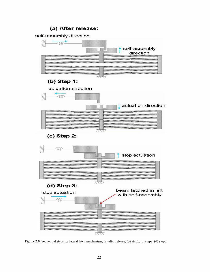
2.1.4.2 Lateral Latch Mechanism
The basic concept of lateral latch mechanism can be presented as a “peg” in a slot, which is
shown in Figure 2.6. The peg can be any shape that mates together with the corresponding slot shape. A
simple rectangular shape is shown in Figure 2.6. The peg may be located on the latch micro-mover with
the slot located on the device micro-mover, as shown in Figure 2.6, or their respective location may be
swapped. The two micro-movers start at zero power with the peg and one of the slots in an engaged
position. This engaged position may be formed through self-assembly of the micro-movers, as shown in
Figure 2.6, or may be formed as drawn in the layout if there is little or no motion from self-assembly. The
device is then set to a new position by a set of sequential steps. In the first step, the latch micro-mover is
electrothermally actuated, pulling the slot away from the peg. In the second step, the device micro-mover
is electrothermally actuated to a new position corresponding to a different second slot. In the third step,
heating power to the latch micro-mover is turned off, and the peg becomes engaged with the second slot.
In the fourth step, heating power to the device micro-mover is turned off, and the slot and peg contact
each other keeping the device in its new position. The latch micro-mover must be designed with adequate
mechanical stiffness to hold the peg in place. As a guideline, the stiffness of the latch mechanism in the
direction of the device micro-mover displacement should be at least 10 times greater than the stiffness of
the device micro-mover. A bi-stable latch mechanism with two slots is shown in Figure 2.6, however any
number of slots can be designed as long as the micro-mover stroke can accommodate the slot placement.
Any number of latch mechanisms can be used with a given device, as long as there is layout area to fit the
required micro-movers.
22
Figure 2.6. Sequential steps for lateral latch mechanism, (a) after release, (b) step1, (c) step2, (d) step3.

23
2.2 RF MEMS Tunable Capacitors
Electrothermal actuators described in Section 2.1.1 are used in RF MEMS tunable capacitors as
the tuning mechanism. The designed tunable capacitors can be classified into two categories based on
their tuning schemes, as: “gap & area tuning” and “gap tuning”. The parallel-plate capacitance equation
without the fringing effects is
gA
C rεε 0= (2.11)
where A is area between parallel plate electrodes, g is the gap between parallel plates, ε0 is the
permittivity of free space = 8.854 pF/m and εr is the dielectric constant of material between plates.
Capacitance can be changed by changing or moving the material between the parallel plates, changing the
gap or changing the area of the electrodes (Figure 2.7). In gap & area tuning topologies, both geometric
parameters are changed simultaneously to achieve high ratios between maximum and minimum
capacitance. In this section, all of the topologies explored for these two categories will be explained, but
modeling of only the more mature capacitor designs will be given due to the drawbacks of the initial
topologies.
(a) (b) (c) (d)
Figure 2.7. Different tuning techniques, (a) dielectric tuning, (b) gap tuning, (c)area tuning, (d) gap &area tuning (Dashed electrodes are the showing the initial position of that electrode).
ε
dielectric tuning
g
gap tuning
A
area tuning gap & area tuning x
yx &y

24
2.2.1 Gap & Area Tuning Topologies
1st Generation Capacitors with Gap & Area tuning:
There are two different designs for 1st generation capacitors. The layout of the first design is
shown in Figure 2.8(a). Interdigitated beams are used for producing the capacitance. Half of the beams
are anchored to the outer frame, and the other half are anchored to the inner frame. The outer frame is the
static frame and the inner frame is the moving frame. The area & gap tuning is designed by using a
polysilicon resistor as a heater inside the inner frame. Upon heating the inner frame and inner beams by
that polysilicon resistor, the interdigitated beams anchored to the inner frame curl down vertically due to
their multilayer nature and also curl sideways due to lateral offset on the beams. When the inner beams
curl down, the area between inner and outer beams decreases. The inner beams curl sideways, which
results in a gap change between electrodes. Two electrothermal actuators are used for a second gap tuning
mechanism for this topology. The outer stator frame is designed as three parallel beams to be curled same
as the inner beams, which is important for curling match between inner and outer beams. There are two
main drawbacks of this design. First, the inner beams curl down and curl sideways upon heating the inner
frame. Curling down decreases the area and results a reduction in the capacitance. Curling sideways
decreases the gap between beams, which increases the capacitance. These two effects are happening at the
same time, and working against each other, to reduce the potential tuning range. The second drawback is
related to the electrothermal actuator. Fixed-fixed beams used in the actuator displace less than a folded-
flexure design.
The second design of the 1st generation gap & area tuning capacitors is shown in Figure 2.8(b).
Again interdigitated beams are used for producing the capacitance. The two drawbacks from the previous
design were solved. Folded-flexure actuators are used. No lateral offsets are designed into the beams, so
there is no lateral curl in the actuator and a mechanical latch mechanism is applied to the design, which
was explained more detail in Section 2.1.4. The stator beams are anchored to two outer frames instead of
one, and the rotor beams are anchored to an inner frame. An electrothermal heater in the inner frame
provides vertical actuation for area tuning. A folded-flexure electrothermal actuator located at the base of

25
the inner frame is used to change the gaps between the beams. The drawback of this design is the large
curl mismatch between the stator and rotor beams, since these beams are not anchored along a common
axis. This curl mismatch results in a greatly reduced overall capacitance.
(a) (b)
(a) (b)
(c) Figure 2.8. Layouts of 1st generation gap & area tuning RF MEMS capacitors, (a) first design in Austria Mikro System (AMS) 0.6 µm CMOS process, (b) second design in Agilent 0.5 µm CMOS process, (c) close view of the beam part with the engaged offset.
A vertical latch mechanism similar to the one in Figure 2.5 is used in the second design. The
vertical electrothermal beam in Figure 2.5(b) corresponds to the inner frame in Figure 2.8(b). For the first
state, when the inner frame latches below the latch actuator, the rotor beams move to a vertical level that
is lower than the stator. At that position, the area between the beams decreases, which results a decrease

26
in capacitance. For the second state, when the inner frame latches above the latch actuator, the stator and
rotor beams are aligned in the same vertical plane. At that position, the area between the beams is
maximum, and therefore capacitance is also maximum.
2nd Generation Capacitors with Gap & Area tuning:
There are two different designs for the 2nd generation capacitors. The layout of the first design is
shown in Figure 2.9(a). An array of interdigitated fingers is used for producing the capacitance of the
designs. The finger array improves the tuning range, compared to the ones with interdigitated beams. By
(a)
(a) (a) (b)
(c) (d) Figure 2.9. Layout of 2nd generation gap & area tuning RF MEMS capacitors, (a) first design in TSMC 0.35 µm CMOS process, (b) layout configuration of fingers, (c) disengaged configuration of fingers, (d) engaged configuration of fingers.
inner yokes
inner yokes inner yokes

27
using the interdigitated fingers, the capacitance per unit area is increased compared to the interdigitated
beams from the 1st generation designs, which results in the tuning range improvement. Folded flexure
electrothermal actuators are connected to each side of the inner rotor frame. The operation of the fingers
is illustrated in Figure 2.9 as layed out (b), engaged (c) and disengaged (d). When the capacitors are
released, the inner frame and fingers are intended to self-assemble to disengage the fingers (Figure
2.9(c)). When the gaps between the finger ends and between the inner and outer beams are 2.3 µm, the
minimum capacitance should be seen. This configuration is named as “disengaged” (Figure 2.9(c)).
Electrothermal actuation is intended to displace the inner frame to engage the fingers (Figure 2.9(d)). The
gap between the fingers is designed to be 0.4 µm and the gap between the inner and the outer beams
should be 8 µm. This design is classified as gap & area tuning, but after the gap between the fingers
becomes 0.4 µm, it is actually only area tuning. The second design of the 2nd generation gap &area tuning
capacitors is aimed for a 0.1 pF to 1 pF capacitance range, which is useful for RF filter design. The 1st
design is aimed for 50 fF to 300 fF capacitance range, because for these ranges the capacitor area is small,
which results in less curl mismatch between the two electrodes of the capacitor.
Both 2nd generation (Figure 2.9) gap & area tuning capacitors include lateral latch mechanisms. In
the first design (Figure 2.9), the dimensions of the peg slots in the latch mechanism were not designed
correctly. The latch mechanism should be symmetric to the y-axis and have at least two groups of peg-
slots. These two mistakes were solved for the second design of the 2nd generation gap & area tuning
capacitors.
The second, revised, design used a lateral latch mechanism similar to the one in Figure 2.6. The
plate with a peg, which is fixed from one side in Figure 2.6, corresponds to the inner frame in Figure
2.10(a). The latch mechanism for this capacitor is symmetric to y-axis and has two groups of peg-slot
structures. The inner frame has two positions, like the plate-actuator in Figure 2.6. For the first position,
when the pegs latch in the slot after self-assembly, the fingers connected to the inner beam move to a
disengaged configuration, as shown in Figure 2.9(c). At that position, gaps between the fingers become

28
4 µm, which results in the minimum capacitance. Similarly for the second position of the latch, after
sequential steps like the ones in Figure 2.6, the fingers connected to inner beam move to an engaged
configuration, as shown in Figure 2.9(d). At that position, gaps between the fingers become 0.6 µm,
which results in the maximum capacitance.
There are two important dimensions of the lateral latch structures, those are distance a and
distance b, as shown in Figure 2.10(b). Distance b is equal to the displacement of the rotor beams from
initial layout to the disengaged configuration (2 µm). Distance a is equal to the displacement from the
disengaged to the engaged configuration (18.4 µm).
(a) (b)
Figure 2.10. (a) layout of 2nd generation gap & area tuning RF MEMS capacitors Jazz 0.35 µm BICMOS process, (b) closer view of latch mechanism.
2.2.1.1 Analytical Calculations for Tuning Ranges and Quality Factors
Building analytical calculations for capacitance specifications is one of the important pieces in
the design process. For RF filter and VCO circuits, a lot of iteration is required for setting center
frequencies, tuning ranges and other circuit specifications like phase noise for VCO’s or quality factor for
distance a distance b

29
RF filter’s. Using finite element analysis (FEA) for these iteration processes is time consuming, so it is
difficult to make all desired iterations by using FEA. This need motivates analytic models for important
capacitor specifications, like CMAX, CMIN and quality-factor versus frequency. In Section 2.2.1.2, after the
simulation results are presented, a comparison between those simulation results and analytic results from
this section will be shown.
(a) (b)
(c) (d)
Figure 2.11. Different configurations to show main and 2nd order parameters for 2nd generation gap & area tuning capacitors, (a) layout view, (b) closer view of finger parts in layout configuration, (c) closer view of finger parts in engaged configuration, (d) closer view of finger parts in disengaged configuration.
Lb
Wf
Wb
d2
d1
Lf
N
n n n
inner beam
Lb
g1 g2
g7
g5 g4 g6
g3

30
Analytical Equations for CMAX and CMIN:
The most mature gap & area tuning capacitors will be analyzed to calculate the maximum and
minimum capacitance. Two equations for the parallel plate will be used for analysis. The first equation
(2.11) neglects the fringing field effects, and the second equation (2.12) is making simple assumption of
fringing fields [46]
++= Lh
ghLC r 220εε (2.12)
where g is the gap between parallel plates, h is thickness, L is the length, A (A=h×L) is area between
parallel-plate electrodes. A closer view of the capacitor is shown in Figure 2.11 to illustrate the design
parameters. The definitions, symbols, and the values for the main parameters to calculate CMAX and CMIN
are shown in Table-2.3.
Table 2.3. Definitions, symbols, and values for main parameters of 2nd generation gap & area tuning RF MEMS capacitors.
There are some other 2nd order parameters, which can be calculated from these main parameters
and are defined in Table-2.4. These parameters will be used in the equations for calculating CMAX and
CMIN . The equations for these 2nd order parameters are shown from (2.13) to (2.19), and all 2nd order
parameters are expressed by main parameters:
Definitions of main parameters for 2nd generation gap & area tuning RF MEMS capacitor
Parameter symbols
Parameter values
Finger width Wf 2.6 µm Finger length Lf 15 µm
Number of finger groups N 5 Number of fingers in one group n 40
Gap between the finger on the side (engaged configuration) g1 0.6 µm Gap between the finger at the tip (engaged configuration) g2 0.6 µm
Distance between fingers (layout configuration) d1 2.0 µm Distance between beams (layout configuration) d2 6.0 µm
Minimum displacement needed for self-assembly d3 2.0 µm Total thickness h ~10.0 µm (confidential)
Beam width Wb 6.0 µm
31
Table 2.4. Definitions and symbols for 2nd order parameters of 2nd generation gap& area tuning RF MEMS capacitors.
313 ddLg f ++= (2.13)
232
214 )()( ddgWg f −++= (2.14)
21
2325 )()( gddLg f +−+= (2.15)
22
16 22
+
+= ff L
gW
g (2.16)
317 ddLg f ++= (2.17)
328 ddg −= (2.18)
( )( )112 gWnL fb +−= (2.19)
Displacement d3 is the amount that the inner frame moves from layout configuration to
disengaged configuration. In Figure 2.11, all main and 2nd order parameters except d3 are indicated in
layout view (a), in the engaged configuration (b) and in the disengaged configuration (c).
CMAX Calculation
CMAX is the total capacitance of the MEMS capacitor when it is in engaged configuration. For the
1st method, (2.11) will be used to find capacitance without fringing fields. When calculating the CMAX, it
can be distributed to three parts: Cenga1 is the total capacitance between the finger parts, Cenga2 is the total
Definitions of 2nd order parameters for 2nd generation gap & area tuning RF MEMS capacitors
Parameter symbols
Finger gaps at the tip (disengaged configuration) g3 Gap between two finger tips (disengaged conf.) g4
Gap between two finger sidewalls (disengaged conf.) g5 Gap between finger tip and sidewall (disengaged conf.) g6
Gap between the beams (engaged configuration) g7 Gap between the beams (disengaged configuration) g8
Beam length Lb
32
capacitance between the trusses and Cenga3 is the total fixed capacitance between one side of the electrode
to the substrate and ground parts around capacitors. Using (2.11), Cenga3 is calculated as 31 fF.
( ) ( )21
1
1212g
hWNng
hLNnC ff
enga
εε −+
−= (2.20)
7
2 ghLN
C benga
ε= (2.21)
The maximum capacitance is
321 engaengaengaMAX CCCC ++= (2.22)
using the main parameters values Table-2.3, the maximum capacitance value is calculated as 868 fF.
When fringing fields are not neglected, (2.12) is then used for the parts of the capacitance with
fringing are
( ) ( )
++−+
++−= f
ff
fenga Wh
ghW
NnLhg
hLNnC 22122212
211 εε (2.23)
++= b
benga Lh
ghL
NC 227
2 ε (2.24)
and Cenga3 is calculated as 39 fF. The maximum capacitance with fringing field is calculated as 1298 fF
from the Table-2.3 parameters. The fringing capacitance accounts for 33.12% of the capacitance.
CMIN Calculation
CMIN is the total capacitance of the MEMS capacitor when it is in disengaged configuration. First,
the minimum capacitance, neglecting fringing will be calculated using a simplistic parallel-plate
portioning as shown in Figure 2.12(a). CMIN can be distributed to three parts: Cdisen1 is the total capacitance
between the fingers. Cdisen2 is the total capacitance between the yokes and Cdisen3 is the total fixed
capacitance between one side of the electrode to the substrate and ground parts around capacitors. Cdisen1
is sum of Cdisen1a, Cdisen1b, Cdisen1c, and Cdisen1d, as defined in Figure 2.12(a).

33
(a) (b)
Figure 2.12. Models to calculate capacitance for disengaged configuration, (a) 1st method, (b) 2nd method.
( )
+++−=+++=
654311111 212
gW
gL
gW
gW
hnNCCCCC ffffddisencdisenbdisenadisendisen ε (2.25)
8
2 ghLN
C bdisen
ε= (2.26)
321 disendisendisenMIN CCCC ++= (2.27)
From the main parameters values in Table-2.3, the minimum capacitance is 128 fF, where Cdisen3 is
calculated to be 31 fF.
To calculate Cdisen1 with fringing fields, the model in Figure 2.12(b) should be used rather than the
one in Figure 2.12(a). If we take the same model, the fringing fields are included more than one time.
( ) ( ) ( )
++++
+
++−= 1
8
11 2212 gLWh
gLgLWh
NnC fff
ffdisen ε (2.28)
++= b
bdisen Lh
ghL
NC 228
2 ε (2.29)
where Cdisen3 is calculated as 39 fF. The CMIN value with fringing fields is calculated as 313 fF from the
values in Table-2.3. These four analytically calculated results will be compared with FEA simulation
results in Section 2.2.1.2.
Left side view is transferred to a model like right side one (dashed lines have same length).
Cdisen1c Cdisen1b
Cdisen1a Cdisen1d
g3
g3

34
Analytical Equations for Quality Factor:
The quality factor (Q) is a measure of the loss of RF MEMS capacitor, and is defined as
cyclelossenergystoredenergyaverage
Q/
= (2.30)
The tunable capacitor is modeled as the series L, C and R model shown in Figure 2.13(a). Impedance, Z,
of the capacitor is
−+=
CLjRZ SS ω
ω 1 (2.31)
The capacitor Q is then
( )( ) SCRZZ
Qω
1ReIm
== (2.32)
The 2nd generation gap & area tuning capacitor will be analyzed to calculate Q versus frequency
from 400MHz to 6GHz. The definitions, symbols, and the values for Jazz process of these new
parameters to calculate Q are shown in Table-2.5. RS in (2.32) is the total resistance coming from metal
interconnect used in the capacitor. The assumption is made that metal layers in parallel and connected
electrically through vias behave as the parallel combination of individual metal lines. Rshe1, Rshe2, Rshe3 and
Rshe4 are the sheet resistances of metal1, metal2, metal3 and metal4 respectively. RS has a component
from the actuators, Ractuator and a component from finger-frame parts, Rfinger_frame .
Table 2.5. Definitions, symbols, and values for parameters to calculate Q of 2nd generation gap& area tuning RF MEMS capacitors.
Definitions of parameters for 2nd generation gap & area capacitor to calculate Q
Parameter symbols
Parameter values in Jazz 0.35 µm
BICMOS process Beam length in the actuator Lbeam 200 µm
Beam width for metal3 in the actuator Wbeam1 1.5 µm Beam width for lower metal layers in the actuator Wbeam2 0.9 µm
Plate length in the actuator Lplate 40 µm Plate width in the actuator Wplate 10 µm
Number of parallel beams in the actuator Nbeam 5 Width of the both moving and static frames Wframe 12.0 µm
Length of the static frame Lframe1 250.0 µm Length of the moving frame Lframe2 360.0 µm

35
RS LS C
(a)
(b) (c)
Figure 2.13. (a) series model for capacitor, (b) capacitor layout to show the parameters that are used for calculating Q, (c) closer view of the actuator to show more parameters.
framefingeractuatorS RRR _2 += (2.33)
platebeamactuator RRR += (2.34)
( )
+
+=21
21
23
1
22
sheshe
sheshe
beambeam
beamshe
beambeam
beambeam RR
RRWN
LR
WNL
R (2.35)
+
=23
232
sheshe
sheshe
plate
plateplate RR
RRWL
R (2.36)
framefingerframefinger RRR +=_ (2.37)
Wbeam2 Wbeam1
Wplate Lplate
Lbeam
Lframe2 Wframe
Lframe1
Nbeam

36
( ) ( )sheTframe
frameframesheT
b
bframe R
WLL
RWNL
R 212 ++= (2.38)
( )sheTf
ffinger RnN
WL
R2
= (2.39)
321421431432
4321
sheshesheshesheshesheshesheshesheshe
sheshesheshesheT RRRRRRRRRRRR
RRRRR
+++= (2.40)
Lbeam, Wbeam1, Wbeam2, Lplate, Wplate, Nbeam, Wframe, Lframe1 and Lframe2 are defined in Figure 2.13(b, c). Lf, Wf,
n, N, Lb, Wb were defined in Table-2.3 previously. The calculated RS is 22.67 ohm for the capacitor in
Jazz 0.35 µm BICMOS process and which is distributed as Ractuator = 1.85 ohm and a Rfinger_frame =
Figure 2.14. Calculated quality factor versus frequency of 2nd generation gap & area tuning RF MEMS capacitors.
18.97 ohm. This calculated RS value of 22.67 ohm and the C = CMIN value of 313 fF are plugged into
(2.28) for frequencies from 400 MHz to 6 GHz to generate a Q versus frequency plot in Figure 2.14. A
comparison between this calculated Q and the measured Q will be presented in Section 3.2.1.
2.2.1.2 Simulation Results for Calculating Capacitance
Simulations for maximum and minimum capacitance will assess the accuracy of the analytical
models. Simulating a whole capacitor design for CMAX and CMIN can take up to 24 hours, and sometimes
simulation results in “out of memory” errors. Decreasing the number of elements or nodes in the FEA

37
model is one method to solve the time issue, but then decreasing the number of nodes can result in a
decrease in the accuracy of the simulation. Splitting the capacitor model into small pieces helps to solve
the time and accuracy issues. By using the parameters from Table-2.3, Table-2.4 and Table-2.5. By using
these parameters, a capacitor 3-D model is built and then split into pieces. FEA simulations for CMAX and
CMIN with these pieces were performed with Coventorware software [43]. In Figure 2.15, the 3D models
of fingers and beams are shown for engaged and disengaged configurations. The results for these
simulations are presented in Table-2.6 along with analytic values for CMAX and CMIN from the previous
section. This comparison shows that analytic values without fringing match best within the simulated
results.
(a) (b)
Figure 2.15. (a) 3-D simulated split part for disengaged configuration, (b) 3-D simulated split part for engaged configuration.
Table 2.6. Comparison between simulated and calculated CMIN CMAX results for 2nd generation gap& area tuning capacitors.
Simulated with FEA
(Coventorware)
Analytic Calculation (without fringing
fields)
Analytic Calculation (without fringing
fields)
CMIN (disengaged) 117 fF 128 fF 313 fF
CMAX (engaged) 969 fF 868 fF 1298 fF
disengaged configuration
engaged configuration
38
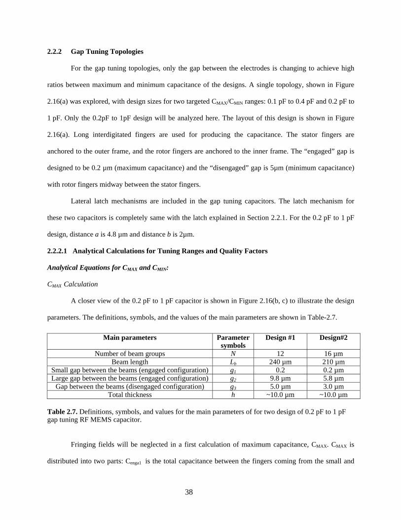
2.2.2 Gap Tuning Topologies
For the gap tuning topologies, only the gap between the electrodes is changing to achieve high
ratios between maximum and minimum capacitance of the designs. A single topology, shown in Figure
2.16(a) was explored, with design sizes for two targeted CMAX/CMIN ranges: 0.1 pF to 0.4 pF and 0.2 pF to
1 pF. Only the 0.2pF to 1pF design will be analyzed here. The layout of this design is shown in Figure
2.16(a). Long interdigitated fingers are used for producing the capacitance. The stator fingers are
anchored to the outer frame, and the rotor fingers are anchored to the inner frame. The “engaged” gap is
designed to be 0.2 µm (maximum capacitance) and the “disengaged” gap is 5µm (minimum capacitance)
with rotor fingers midway between the stator fingers.
Lateral latch mechanisms are included in the gap tuning capacitors. The latch mechanism for
these two capacitors is completely same with the latch explained in Section 2.2.1. For the 0.2 pF to 1 pF
design, distance a is 4.8 µm and distance b is 2µm.
2.2.2.1 Analytical Calculations for Tuning Ranges and Quality Factors
Analytical Equations for CMAX and CMIN:
CMAX Calculation
A closer view of the 0.2 pF to 1 pF capacitor is shown in Figure 2.16(b, c) to illustrate the design
parameters. The definitions, symbols, and the values of the main parameters are shown in Table-2.7.
Table 2.7. Definitions, symbols, and values for the main parameters of for two design of 0.2 pF to 1 pF gap tuning RF MEMS capacitor.
Fringing fields will be neglected in a first calculation of maximum capacitance, CMAX. CMAX is
distributed into two parts: Cenga1 is the total capacitance between the fingers coming from the small and
Main parameters Parameter symbols
Design #1 Design#2
Number of beam groups N 12 16 µm Beam length Lb 240 µm 210 µm
Small gap between the beams (engaged configuration) g1 0.2 0.2 µm Large gap between the beams (engaged configuration) g2 9.8 µm 5.8 µm
Gap between the beams (disengaged configuration) g3 5.0 µm 3.0 µm Total thickness h ~10.0 µm ~10.0 µm

39
large gap side, and Cenga2 is the total fixed capacitance between one side of the electrode to the substrate
and ground parts. Cenga2 is calculated as 29 fF.
(a) (c)
Figure 2.16. (a) Different configurations to show main parameters for 2nd gap tuning capacitors (a) layout view, (b) closer view of beam parts in disengaged configuration, (c) closer view of finger parts in engaged configuration.
21
1 ghLN
ghLN
C bbenga
εε+= (2.41)
211 engaengaMAX CCC += (2.42)
Using parameter values from Table-2.7, the CMAX value without fringing is 1284 fF for design#1
and 1514 fF for design#2. The capacitance including fringing field, uses a different equation for engaged
capacitance
+++
++= b
bb
benga Lh
ghL
NLhg
hLNC 2222
211 εε (2.43)
Lb Lb g3
N
g2
g1
(b)
40
Cenga2 is calculated as 29 fF. The maximum capacitance value with fringing is calculated as 1398 fF for
design#1 and 1645 fF for design#2.
CMIN Calculation
The minimum capacitance neglecting fringing fields, can be distributed to two parts Cdisen1 and
Cdisen2 , corresponding to the partitioning from the CMAX calculations.
3
12
ghLN
C bdisen
ε= (2.44)
Cdisen2 is calculated as 37 fF. the CMIN value without fringing is calculated as 128 fF for design#1 and 221
fF for design#2.
With fringing fields
+= b
bdisen Lh
ghL
NC 2223
1 ε (2.45)
and Cdisen2 is calculated as 37 fF. The CMIN value with fringing is calculated as 242 fF for design#1 and
354 fF for design #2.
Analytical Equations for Quality Factor:
The calculations of Q for gap tuning capacitor design in Jazz 0.35 µm BICMOS process are
similar to these done in Section 2.2.1.1. Calculations from (2.36) to (2.38) for Ractuator are same with this
capacitor design. The parameter values of the gap tuning designs are: Lbeam = 180 µm, Nbeam = 4, Wb = 3
µm, Lframe1 = 190µm and Lframe2 = 290µm. The calculated value for Ractuator is 2.064 Ω. The equation for RS
and Rframe are different and given by
framebeamactuatorS RRR _2 += (2.46)
framebeamframebeam RRR +=_ (2.47)
( )sheTframe
frameframeframe R
WLL
R 21 += (2.48)

41
( ) ( )sheT
b
bframe R
WLN
R12 +
= (2.49)
The calculated Rs value of 20.42 Ω and the C value of 221 fF were plugged into (2.28) for
frequencies from 400 MHz to 6 GHz to generate the Q versus frequency plot in Figure 2.17.
Figure 2.17. Analytically calculated quality factor versus frequency of gap tuning design#2.
2.2.2.2 Simulation Results for Calculating Capacitance
FEA and calculated results for design#1 are shown in Table-2.8. The analytic calculation without
fringing fields comes closest to the FEA results.
Table 2.8. Comparison between simulated and calculated CMIN CMAX results for gap tuning design#1.
Simulated with FEA
(Coventorware)
Analytic calculation (without fringing
fields)
Analytic calculation (with fringing
fields)
CMIN (disengaged) 180fF 128 fF 242 fF
CMAX (engaged) 1026 fF 1284 fF 1398 fF

42
Chapter 3. Experimental results
Characterizing the fabricated devices is an important step in the design flow. To assess the
accuracy of the models from Chapter 2, characterization results will be examined by comparing them with
the analytical and simulation results. In Section 3.1, experimental measurement of the displacement and
frequency response of micro-mover test structures will be presented. The performance of tunable
capacitors that use the micro-movers and latch mechanisms will be presented in Section 3.2.
3.1 Characterization of Self Assembling and Electrothermal Actuators
Characterization results for various micro-mover designs in different CMOS/BICMOS processes
will be presented in this section. Three basic characterizations include self assembly lateral displacement,
electrothermal lateral displacement versus temperature (or input power) and frequency response to
measure thermal time constant and mechanical resonance frequency. For some recent micro-mover
designs, a brief comparison between the measured results and the analytic-simulated results will be
presented. More detailed comparisons and discussions will be presented in Section 4.1.
3.1.1 Lateral Displacement from Self-assembly
The scanning electron micrographs (SEM) of fabricated micro-movers in the AMS 0.6 µm
CMOS process and the Agilent 0.5 µm CMOS process are given in Figure 3.1(a, b). Self-assembly
displacements in these processes are measured by taking close-up SEMs of the moving piston and
comparing with the layout view. In the AMS 0.6 µm CMOS process, measured lateral self-assembly
displacement is 6.8 µm for a 3-metal micro-mover with the design parameters: Lbeam= 100 µm, Wbeam1=
1.5 µm, Wbeam2= 0.9µm, Lplate= 40 µm, Wplate = 8 µm, doffset = 0.3 µm and Nbeam= 3. In the Agilent 0.5 µm
CMOS process, measured lateral self-assembly displacement is 2.3 µm for a micro-mover with the same
design parameters. The direction of the self-assembly is as predicted in Section 2.1.1 in the AMS 0.6 µm
CMOS process and that shows that the all-oxide side of the beam is more compressive than the side with
embedded metal layers. The self-assembly direction is in the opposite direction in the Agilent 0.5 µm

43
CMOS process, indicating that the all-oxide side of the beam is less compressive than the side with the
embedded metal layers.
Scanning electron micrographs of fabricated micro-movers in the TSMC 0.35 µm CMOS process
are given in Figure 3.2(a, b). In the TSMC 0.35 µm CMOS process, the measured lateral self-assembly
displacements are 0.3 µm for both full and half size 4-metal micro-movers with the same design
parameters as above. The direction of the self-assembly is same as predicted in Section 2.1.1.
(a) (a) (b) Figure 3.1. Scanning electron micrograph of fabricated micro-movers, (a) in AMS 0.6 µm CMOS process, (b) in Agilent 0.5 µm CMOS process.
(a) (b) Figure 3.2. Scanning electron micrograph of fabricated micro-movers in TSMC 0.35 µm CMOS process, (a) full-size actuator, (b) half-size actuator.
The scanning electron micrographs of a fabricated micro-mover in the Jazz 0.35 µm BICMOS
process are given in Figure 3.3(a). The verniers at the side of the moving piston and at the static parts aid
in measuring lateral displacement, as shown in Figure 3.3(b). By using these verniers, 0.1 µm resolution
can be achieved. The comparison between the measured and simulated self-assembly displacements for
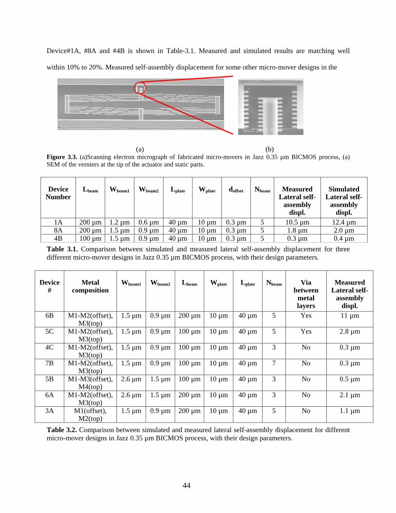
44
Device#1A, #8A and #4B is shown in Table-3.1. Measured and simulated results are matching well
within 10% to 20%. Measured self-assembly displacement for some other micro-mover designs in the
(a) (b) Figure 3.3. (a)Scanning electron micrograph of fabricated micro-movers in Jazz 0.35 µm BICMOS process, (a) SEM of the verniers at the tip of the actuator and static parts.
Table 3.1. Comparison between simulated and measured lateral self-assembly displacement for three different micro-mover designs in Jazz 0.35 µm BICMOS process, with their design parameters.
Table 3.2. Comparison between simulated and measured lateral self-assembly displacement for different micro-mover designs in Jazz 0.35 µm BICMOS process, with their design parameters.
Device
Number
Lbeam
Wbeam1
Wbeam2
Lplate
Wplate
doffset
Nbeam
Measured
Lateral self-assembly
displ.
Simulated
Lateral self-assembly
displ. 1A 200 µm 1.2 µm 0.6 µm 40 µm 10 µm 0.3 µm 5 10.5 µm 12.4 µm 8A 200 µm 1.5 µm 0.9 µm 40 µm 10 µm 0.3 µm 5 1.8 µm 2.0 µm 4B 100 µm 1.5 µm 0.9 µm 40 µm 10 µm 0.3 µm 5 0.3 µm 0.4 µm
Device
#
Metal
composition
Wbeam1
Wbeam2
Lbeam
Wplate
Lplate
Nbeam
Via
between metal layers
Measured
Lateral self-assembly
displ. 6B M1-M2(offset),
M3(top) 1.5 µm 0.9 µm 200 µm 10 µm 40 µm 5 Yes 11 µm
5C M1-M2(offset), M3(top)
1.5 µm 0.9 µm 100 µm 10 µm 40 µm 5 Yes 2.8 µm
4C M1-M2(offset), M3(top)
1.5 µm 0.9 µm 100 µm 10 µm 40 µm 3 No 0.3 µm
7B M1-M2(offset), M3(top)
1.5 µm 0.9 µm 100 µm 10 µm 40 µm 7 No 0.3 µm
5B M1-M3(offset), M4(top)
2.6 µm 1.5 µm 100 µm 10 µm 40 µm 3 No 0.5 µm
6A M1-M2(offset), M3(top)
2.6 µm 1.5 µm 200 µm 10 µm 40 µm 3 No 2.1 µm
3A M1(offset), M2(top)
1.5 µm 0.9 µm 200 µm 10 µm 40 µm 5 No 1.1 µm

45
Jazz 0.35 µm BICMOS process are given in Table-3.2, with their design parameters. The designs in
Table-3.2 do not have field oxide under the lowest metal layer.
3.1.2 Lateral Displacement from Electrothermal Actuation
Lateral displacements from electrothermal actuation in the TSMC 0.35 µm CMOS process and
the Jazz 0.35 µm BICMOS process will be presented in this section. Figure 3.4 is showing the
electrothermal lateral displacement versus input power both half-size and full-size actuators in TSMC
0.35 µm CMOS process. Both actuators have the same design parameters: Lbeam= 100 µm, Wbeam1= 1.5
µm, Wbeam2= 0.9µm, Lplate= 40 µm, Wplate = 8 µm, and Nbeam= 3. The full-size actuator has approximately
60% of the displacement at the same power input.
Figure 3.4. Electrothermal lateral displacement versus input power for half-size and full-size actuators in TSMC 0.35 µm CMOS process.
The lateral displacements from electrothermal actuation in Jazz 0.35 µm BICMOS process are
measured at different temperatures (325 K, 350 K, 375 K, 400 K, 425 K, 450 K). The comparison
between the measured and simulated electrothermal lateral displacements for Device#1A and #8A is
shown in Table-3.3. Measured and simulated results are matching well within 10% to 20%.
3.1.3 Frequency Response and Thermal Time Constant
Mechanical frequency response due to thermal heating can be determined by measuring the
lateral displacement optically at different frequencies using a MIT microvision system [47]. Measurement

46
results are shown in Figure 3.5(a, b) for a micro-mover in the Jazz 0.35 µm BICMOS process with the
design parameters: Lbeam= 168 µm, Wbeam1= 1.5 µm, Wbeam2= 0.9µm, Lplate= 43 µm, Wplate = 12 µm, and
Nbeam= 5.
(a)
(a) (b) Figure 3.5. Mechanical frequency response of the micro-mover during the electrothermal actuation. (a) 10 Hz to 600Hz. (b) 3 kHz to 200 kHz.
For the first step of characterization, measurements are taken from 10 Hz to 600 Hz to capture the
f3dB bandwidth and the thermal time constant. The measured values are f3dB = 178 Hz andτ = 1.12 ms.
Measured and analytically calculated τ results are matching within 11.6%. For the second step of
characterization, measurements are taken from 3 kHz to 200 kHz to capture the mechanical resonant
frequency. The measured value is fres = 26.3 kHz, while the calculated value using layout dimensions is
36.9 kHz. Because of the considerably big difference between measured and calculated value, the
parameter, Wbeam1, is measured by taking a close view of the beam (Figure 3.6(a)). The measured value is
Wbeam1 = 1.3 µm. When this measured value is entered to (2.10), the calculated value is found to be 30.5
kHz. With this consideration, measured and analytically calculated results are matching to within 15.9%.
3.1.4 Nanometer-scale Gap-closing Mechanism
A 1st generation nanometer-scale gap-closing mechanism is designed in the TSMC 0.35 µm
CMOS process. Because of the small lateral displacement from self-assembly, the micro-movers did not
f3dB
fres
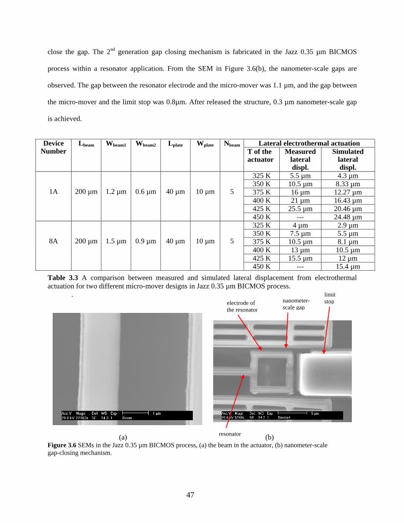
47
close the gap. The 2nd generation gap closing mechanism is fabricated in the Jazz 0.35 µm BICMOS
process within a resonator application. From the SEM in Figure 3.6(b), the nanometer-scale gaps are
observed. The gap between the resonator electrode and the micro-mover was 1.1 µm, and the gap between
the micro-mover and the limit stop was 0.8µm. After released the structure, 0.3 µm nanometer-scale gap
is achieved.
Table 3.3 A comparison between measured and simulated lateral displacement from electrothermal actuation for two different micro-mover designs in Jazz 0.35 µm BICMOS process.
.
(a)
(a) (b)
Figure 3.6 SEMs in the Jazz 0.35 µm BICMOS process, (a) the beam in the actuator, (b) nanometer-scale gap-closing mechanism.
Lateral electrothermal actuation Device Number
Lbeam Wbeam1 Wbeam2 Lplate Wplate Nbeam T of the actuator
Measured lateral displ.
Simulated lateral displ.
325 K 5.5 µm 4.3 µm 350 K 10.5 µm 8.33 µm 375 K 16 µm 12.27 µm 400 K 21 µm 16.43 µm 425 K 25.5 µm 20.46 µm
1A
200 µm
1.2 µm
0.6 µm
40 µm
10 µm
5
450 K --- 24.48 µm 325 K 4 µm 2.9 µm 350 K 7.5 µm 5.5 µm 375 K 10.5 µm 8.1 µm 400 K 13 µm 10.5 µm 425 K 15.5 µm 12 µm
8A
200 µm
1.5 µm
0.9 µm
40 µm
10 µm
5
450 K --- 15.4 µm
resonator
electrode of the resonator
nanometer-scale gap
limit stop

48
3.2 Characterization of RF MEMS Tunable Capacitors
Characterization results for various capacitor designs in different CMOS and BICMOS processes
will be presented in this section. The designs are listed in Table 3.4 with selected measured values. These
characterizations include quality factor versus frequency for 400 MHz to several gigahertz (3-6 GHz) and
capacitance versus control voltage. Data for quality factor and tuning characteristic measurements were
taken by measuring the scattering(S)-parameters with an Agilent E8364A network analyzer. Custom
matlab code, listed in Appendix 1, converts from S-parameters to quality factor and capacitance values.
The detailed post-CMOS micromachining flows are given in Appendix 2 for each foundry process used.
Table 3.4 Selected characterization results for different designs.
3.2.1 Gap & Area Tuning Topologies
1st Generation Capacitors with Gap & Area tuning:
There are two different designs for 1st generation capacitors, one, AMS1, in the AMS 0.6 µm
CMOS process and a later design, Agilent1, in the Agilent 0.5 µm CMOS process. The scanning electron
micrographs of fabricated 1st generation capacitors are shown in Figure 3.7(a) and Figure 3.8(a). During
CMOS post-processing, no releasing problems were observed.
Design AMS1 has a measured off capacitance of 153 fF and a measured Q of 24 at 1.5 GHz. The
capacitance change at 1.5 GHz is measured from 153 fF to 175 fF within a 12 V control voltage and
25.5 mW actuator power. Measured tuning range is 14.4%, which is smaller than expected due to the
lateral finger curl and fixed-fixed actuator issues explained in Section 2.2.1. The fingers exhibit excessive
lateral beam curling, as shown in Figure 3.7 (b), to the point where the fingers touch each other by self-
assembly. The snapped beams cannot move from their positions, and so cannot be tuned (Figure 3.7(b)).
Design # Tuning
Range
Process Layout dimensions (µm×µm)
CMIN (fF)
CMAX (fF)
Q @ 1.5GHz
Power (mW)
VTUNE (V)
AMS1 14.4% AMS 0.6 µm CMOS 170×220 153 175 24 25.5 12 Agilent1 35.9% Agilent 0.5 µm CMOS 230×270 209 284 28 72 24 TSMC1 352.4% TSMC 0.35 µm CMOS 228×250 42 148 52 34.2 12
Jazz1 36% Jazz 0.35 µm BICMOS 390×500 280 380 5 12 4 IBM1 18% IBM 6HP 0.25 µm BICMOS 220×350 265 313 17 13 4

49
(a) (b) (a) (b) Figure 3.7. Scanning electron micrograph (SEM) of fabricated 1st generation gap & area tuning RF MEMS capacitors, (a) AMS1 design in AMS 0.6 µm CMOS process, (b) close view of snapped interdigitated beams in the AMS1 design.
Design Agilent1 has a measured capacitance change at 1.5 GHz 209 fF to 284 fF within a 24 V
control voltage, and 72.4 mW actuator power, corresponding to a measured tuning range of 35.9%. The
tuning characteristic is shown in Figure 3.9(b). The observed behavior between capacitance and
controlling voltage is opposite from the original design intention. Increasing heating power was expected
to decrease the capacitance, as the finger gap increased. The reason for the measured behavior is due
initial curl mismatch between adjacent fingers. When the inner frame is heated, it curls down as expected.
However, the fingers also curl down, since they are also heated. The net effect is that the finger sidewall
overlap area increases with heating. The vertical latch mechanism did not work, because the
electrothermal actuators in Agilent 0.5 µm CMOS process displaced laterally in an opposite way of the
intended direction upon release. Measured S11 parameters of the Agilent1 design is shown in Figure 3.8(b)
from 45 MHz to 3 GHz.

50
(a) (b)
(a) (b) Figure 3.8. (a) Scanning electron micrograph (SEM) of a fabricated Agilent1 design, (b) Measured S11 parameters of the Agilent1 design.
(a) (b)
(a) (b) Figure 3.9. RF characterization of the Agilent1 design, (a) measured quality factor from 400 MHz to 3GHz, (b) measured tuning characteristic (capacitance versus controlling voltages).
45 MHz
3 GHz

51
Measured Q values at minimum capacitance versus frequency from 400MHz to 3GHz are shown
in Figure 3.9(a). The device has a Q above 38 up to 1 GHz and is 28 at 1.5 GHz. The power and the
controlling voltages are larger for Agilent1 design, because the area of the capacitor and capacitance
range of the Agilent1 design is bigger than the ones for AMS1 design.
2nd Generation Capacitors with Gap & Area tuning:
The 2nd generation capacitors are the TSMC1-4 and Jazz1 designs listed in Table 3.4 and Table
3.5. No releasing problems were observed for the TSMC 0.35 µm CMOS process.
Four different test capacitors were designed for the finger design topology in the TSMC 0.35 µm
CMOS process. Three design parameters are changed. The first parameter is the type of the tuning
actuator, called “half-size” and “full-size”. A capacitor with a full-size actuator is shown in Figure
3.10(a), and one with a half-size actuator is shown in Figure 3.10(b). The second parameter, the number
of finger yokes, is either 4 or 6. One finger yoke is identified in Figure 3.11(a). The third parameter is the
offset of the lower metal layers in the electrothermal actuator parts. Some of the capacitors have offset on
one side of the actuator beams, while others offset on the opposite side. When these capacitors were
designed, the direction of electrothermal motion and self-assembly was not known. The summary of the
experimental results of different TSMC test devices for area, CMAX, CMIN, tuning range, controlling
voltage (VTUNE), actuator power and Q are shown in Table-3.5.
Table 3.5. Experimental results for tunable capacitors in 0.35 µm TSMC CMOS process.
Measured tuning ranges are larger than those for the prior AMS1 and Agilent1 designs. The main
reason for this improvement in tuning range is the finger-yoke design. The measured tuning
characteristics for the TSMC1 and TSMC4 devices are shown in Figure 3.12(a) and (b) respectively. For
Design # Tuning Range
Actuator, Finger Yokes
Layout dimensions (µm×µm)
CMIN (fF)
CMAX (fF)
Q @ 1.5GHz
Power (mW)
VTUNE (V)
TSMC1 352.4% Full, 6yokes 228×250 42 148 52 34.2 12 TSMC2 352.4% Full, 4yokes 228×230 40 98 40 27.1 12 TSMC3 352.4% Half, 6yokes 150×250 53 108 35 22.4 6 TSMC4 352.4% Half, 4yokes 150×230 35 102 48 18.3 6

52
both of the devices in Figure 3.11 and Figure 3.12, the opposite offset direction compared to the layout of
the actuator in Figure 2.1 was designed. Unfortunately the measured motion is the opposite of the desired
(a) (b)
(a) (b) Figure 3.10. Scanning electron micrograph (SEM) of a fabricated TSMC1 and TSMC3 gap & area tuning capacitor, (a) TSMC1 capacitor with full-size actuators (b) TSMC3 capacitor with half-size actuators.
motion to engage the fingers. The correct orientation of the offset of metal layers in the actuator beams
was not known when designed. In Figure 3.12, after releasing the capacitor, the inner frame displaces due
to self-assembly and the fingers move to their engaged position. The fingers become disengaged, when
the controlling voltage is around 3 V for the capacitor design with half size actuators and 6 V for the one
with full-size actuators. The gaps between the fingers and between the inner and outer beams are 2.3 µm,
when the minimum capacitances are encountered, as seen in Figure 3.12. If the controlling voltages are
increased, the inner frame moves further and maximum capacitance is achieved when the inner yokes and
outer yokes get closer to each other. For the engaged position, the capacitance values are 4 times lower
than expected, because the finger did not engage all the way. The fingers only engaged 1 µm into 4.6 µm
deep-gap. Processing issues contributing to the inability to engage included the presence of a polymer
film on the sidewalls of the fingers and the bloating of the top metal-4 layer. The net effect is that the

53
(a) (b)
(a) (b) Figure 3.11. (a) one finger yoke in a capacitor, which has 4 finger yokes, (b) measured quality factor from 400 MHz to 3GHz for TSMC4 capacitor with half-size actuators and 4 finger yokes.
(a) (b)
(a) (b) Figure 3.12. Measured tuning characteristic (capacitance versus controlling voltages) of 2nd generation gap & area tuning capacitors, (a) TSMC1 capacitor with full-size actuator and 6 finger yokes, (b) for TSMC4 capacitor with half-size actuator and 4 finger yokes.

54
fingers are wider than the layout dimension by about 0.3 µm. The latch mechanism did not work, because
of the incorrect design orientation of the actuator metal offsets.
Measured Q values (at minimum capacitance) versus frequency from 400MHz to 3GHz for the
TSMC4 device, which employs 4 finger groups and half-size actuators are shown in Figure 3.11(b).
These 2nd generation capacitor designs have higher Q values and less power consumption compared to 1st
generation designs. All 4 metals layers are used in parallel to decrease the series resistance. In contrast,
the 1st generation designs employ only three metal interconnect layer in parallel.
The scanning electron micrograph of a fabricated Jazz1 2nd generation capacitor is shown in
Figure 3.13(a). During BICMOS post-processing, some micro-masking was observed, as indicated in
called micro-masking Figure 3.13(b). The micro-masking problem mainly depends on the die area
dimensions of the BICMOS chip. For the Jazz process, the die dimensions are 5mm by 5mm, which is
bigger than the prior runs in the other foundries (3mm by 3mm). There are two ways to solve this
problem by reducing these dimensions; one way is to dice the chip to 4 small quarters, and the second
way used here is to block the undesired areas on the chip by using captone tape before the post-
processing.
The latch mechanism worked for the disengaged state, but did not work the intended way for
engaged state. The observed self-assembly direction is the same as predicted. Starting from layout view in
Figure 2.10(b), the tuning frame moves in the east direction, and the latch actuator displaces to north
direction. After these two sequences, the latch mechanism for the disengaged state is shown in the SEM
(Figure3.13(c)). For the intended engaged state, the fingers move west and engage together by using
electrothermal actuation, but due to the finger width bloating, the fingers did not engage. An alternate
way to get a higher capacitance from the same capacitor design is to use self-assembly to close the gaps
between the inner yokes and outer yokes. This is a different state than these intended one, but it worked as
shown in (Figure 3.13(d)). This state is named the “engaged-yokes” state. The measured capacitance is
280 fF for the disengaged configuration and 380 fF for engaged-yokes state corresponding to a tuning
range of 36%. This is lower than predicted, since the fingers did not engage. A comparison for CMIN

55
between the measured, simulated (FEA) and analytically calculated results is shown Table 3-6. Analytical
equations with fringing fields match with the measured results better than the simulation and analytic
calculation with no fringing. A comparison between the measured and analytically calculated Q values (at
minimum capacitance) versus frequency from 800MHz to 6GHz is shown in Figure 3.14. Measured and
(a) (b)
(a) (b)
(a) (b)
(c) (d) Figure 3.13. Scanning electron micrograph (SEM) of a fabricated Jazz1 capacitor, (a) released tunable capacitor, (b) micro-masking problem, (c) capacitor in disengaged state, (d) capacitor in engaged-yokes state (not intended originally).

56
calculated results are matching well at 5-6 GHz, but the measured Q stays at around 5 for lower
frequencies.
Table 3.6. Comparison between simulated, calculated and measured CMIN results for the Jazz1 2nd generation gap & area tuning capacitors.
Figure 3.14 Comparison between calculated and measured Q versus frequency for the Jazz1 gap & area tuning capacitor.
3.2.2 Gap Tuning Topologies
For gap tuning topologies, the first capacitor (IBM1) was designed in IBM SiGe6HP 0.25 µm
BICMOS process, and the second capacitor (Jazz2) was designed in Jazz 0.35 µm BICMOS process. The
SEM of fabricated IBM1 capacitor is shown in Figure 3.15(a). During BICMOS post-processing, a micro-
masking problem similar to that encountered with the previous Jazz chips was again observed. For the die
in the IBM 6HP process, dimensions are 3mm by 3mm and the problem was solved by using the dicing
method. The latch mechanism worked for disengaged state, but did not work the intended way for the
Simulated with FEA
(Coventorware)
Calculated (without fringing
fields)
Calculated (with fringing
fields)
Measured
CMIN (disengaged) 117 fF 128 fF 313 fF 280 fF

57
engaged state (Figure 3.15(b, c)). The behavior is similar to the engaged-yokes state in Figure 3-13(d) for
the Jazz1 design. The capacitance is 265 fF in the disengaged position, and 313 fF in the engaged-yokes
position, resulting in a tuning range of 18%. The measured quality factor is 15 at 1.7 GHz for CMIN.
(a) (a)
(a)
(b) (c) Figure 3.15. Scanning electron micrograph (SEM) of a fabricated IBM1 gap tuning capacitors, (a) released tunable capacitor, (b) capacitor in disengaged state, (c) capacitor in engaged-yokes state.
The Jazz2 capacitor did not release, due to polymer layers on the sidewalls of the fingers. The
tuning operation has not been achieved, because of that processing problem. A comparison between the
measured and analytic Q values (at minimum capacitance) versus frequency from 1.2GHz to 6GHz is
shown in Figure 3.16. Measured Q is about a factor of two greater than the calculations over the entire
frequency range.
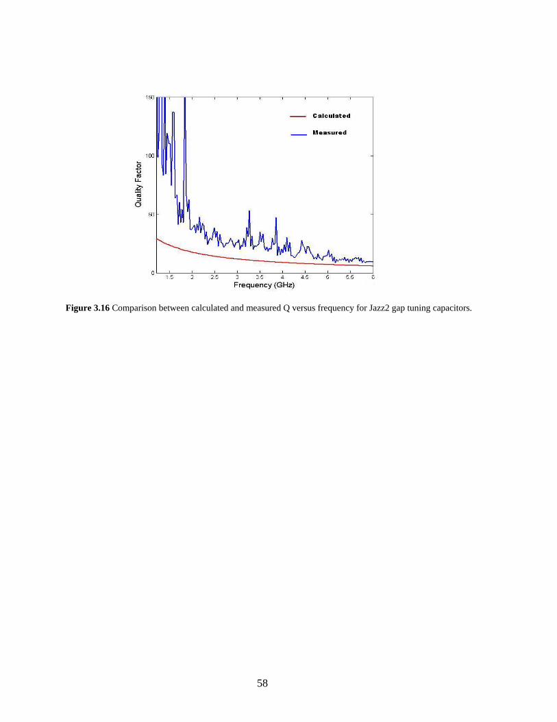
58
Figure 3.16 Comparison between calculated and measured Q versus frequency for Jazz2 gap tuning capacitors.

59
Chapter 4. Discussion and Conclusions
4.1 Discussion
Micro-movers with different design parameters are fabricated and tested to understand the scaling
laws for self assembly and electrothermal actuation as a function of these parameters. To understand the
scaling of self-assembly with beam length, Lbeam, three direct comparisons can be made from results in
Table 3.1 and Table 3.2: between Device#8A and #4B, between Device#6B and #5C and between
Device#5B and #6A. When the parameter value for Lbeam is doubled, the lateral self-assembly
displacement increases almost four times. Similarly to understand the scaling of self-assembly with the
design parameter of having vias between metal layers, two comparisons can be made: between
Device#8A and #6B and between Device#4B and #5C. Having vias on the beams of the actuator
increases the lateral self-assembly displacement around seven times, compared to the designs without
vias. To understand the scaling of self-assembly and electrothermal actuation with the beam width,
Wbeam1, and embedded metal width, Wbeam2, only one comparison, between Device#8A and #1A, can be
made. Changing Wbeam1 from 1.5 µm to 1.2 µm and Wbeam2 from 0.9 µm to 0.6 µm at the same time
increases the lateral self-assembly displacement by 5.8 times, and the electrothermal displacement by 1.5
times.
There are some limits for the design parameters of micro-movers related to process limits. The
embedded metal limit, Wbeam2, cannot be less than 0.5 µm for most of the commonly used CMOS and
BICMOS processes. To get the same ratio between Wbeam1 and Wbeam2 as in Device#1A and Device#8A,
Wbeam1 should be between 0.8 µm or 0.9 µm. A design with these small parameter values will be more
sensitive to process variations, like misalignment and bloat, which can be 0.1 µm to 0.2 µm depending on
the processes. Misalignment would result in undesirable asymmetric beam-bending behavior for the
folded-flexure micro-mover design.
To achieve faster switching time from micro-mover designs, the thermal capacitance must
decrease, or the thermal resistance must increase as seen from (2.7). Increasing thermal conductance

60
results in less thermal isolation, which raises the power required for actuator operation. That technique
can be efficient for some applications like mechanical latch structures, but it is not efficient in general.
Thermal capacitance, C, can be decreased by changing the design topologies. Heating only the beams in
the actuator instead of the whole actuator would be one technique to decrease C. By using this technique
to modify the micro-mover design in Section 2.1.3.3, the calculated C can be reduced to 4.61×10⁻⁸J/K and
f3dB can be increased to 180 Hz from 127 Hz. The improvements are more impressive for the designs with
vias between metal layers. For the same displacement, those designs have smaller Lbeam compared to the
designs without vias. Having smaller Lbeam decreases dramatically the thermal mass coming from beams
in the actuator.
The lateral latch mechanism for the most mature design operates sequentially as intended. The
most important reason for the failure for earlier designs is that the latch mechanisms were designed
without the detailed characterization of self-assembly and electrothermal actuation. For some processes
such as the TSMC 0.35 µm CMOS, the self-assembly displacement is so small, it is difficult to design a
compact mechanical latch.
The quality factor for the most mature gap tuning actuator is quite high compared to the earlier
designs. The measured Q is 52 at 1.7 GHz for 400 fF nominal capacitance (Figure 3.16). Q of 52 at
1.5 GHz for 42fF nominal capacitance is also achieved for a gap & area tuning capacitor design in TSMC
0.35 µm CMOS (Table-3.5). When comparing Q values at a frequency from different capacitor designs,
the nominal capacitance value should also be same for both of the cases, because capacitance affects the
Q, a shown in (2.34). Scaling the capacitance, the most mature design has 10 times better Q than the
earlier gap & area tuning design. To increase the Q, series resistance through the capacitor is reduced. The
sheet resistance is very small for thick metal layers in advanced BICMOS processes, like the Jazz
0.35 µm BICMOS. A great improvement in Q (2 times better) is achieved by using the static frame as the
signal electrode, and the rotor frame as the ground electrode. This technique is used in the most mature
gap tuning actuator.

61
The largest tuning factor from designs to date is 352% for a gap & area tuning capacitor design in
TSMC 0.35 µm CMOS (Table-3.5). This range is large, compared to the previous work. The most
important drawback of this design is the small magnitude of the maximum and minimum capacitance
value, which makes it impossible to be used for RF filters and VCOs in the 1 GHz to 5 GHz frequency
range. Even if these designs are used in the LC tanks with big inductors, poor Q value of the capacitors at
those high frequencies makes it impossible to be used for high performance circuits. The tuning range for
the most mature gap & area tuning capacitor in the Jazz 0.35 µm BICMOS is expected to be 800%, but it
is measured as 36%. The reason for this low tuning range is that the fingers do not engage together. A
polymer layer deposited on the sidewalls of the fingers during post-CMOS processing makes 0.6 µm gap
smaller. Additionally, the top thick metal layer is bloated. The measured width of the fingers with this top
metal layer is larger than its width in the layout, which makes the gap even smaller. New capacitors can
be designed with bigger finger gaps like 1.0 µm to make the design less sensitive to those two problems.
If gap & area and gap tuning topologies are compared for tuning range, gap & area tuning ones
are better, due to having two different tuning mechanisms at the same time. If the same comparison is
made for Q, it is found that gap tuning is better, since there is less series resistance of fingers for the same
capacitance value. If the information from self assembly and electrothermal actuation directions are not
known by the designer during the design process, the gap area tuning is better, as it is not sensitive to the
direction of self-assembly and electrothermal actuation.
The measured and simulated minimum and maximum capacitance values are matched within
10%, as shown in Table 3.6. To increase the accuracy of these analytic calculations, the models built in
Chapter 2 must be revised and fringing effects must be included that are more accurate.
4.2 Conclusions
This research demonstrated a technology to design micro-movers fabricated on CMOS/BICMOS
chips, which can be used for various applications, like tunable passive devices, RF switches or micro-
probes, mechanical latch structures. The tuning range and Q specifications of the fabricated devices point
to a significant improvement in power and agility of VCO’s and RF filters that use these new RF-MEMS

62
components. Future work should be done to increase the efficiency of Capacitance/Area. The reduction of
parasitic capacitance on chip will greatly improve the overall Q of applications in LC tanks.
Mechanical latch and nanometer-gap closing mechanisms are proven feasible. More work to
refine designs must be done. One future work can be done to employ new micro-mover designs like the
ones with vias between metal layers by these mechanisms to give the same displacements from smaller
area. This way the overall area for the designs can be reduced. Designing a technique to package these
mechanisms and also the tunable capacitor should be investigated to reduce cost per device.
63
Bibliography
[1] R. Borwick, P. Stupar, J. Denatale, R. Anderson, C. Tsai, and K. Garret, “A high Q, large tuning range tunable capacitor for RF applications,” in IEEE MEMS Conf. Tech. Dig., 2002, pp. 669–672.
[2] C. Tsai; P.A. Stupar, R.L. Berwick, P. Minfan, L. DeNatale, “An isolated tunable capacitor with a
linear capacitance voltage behavior,” in 2003 IEEE Int. Conference on Solid-State Sensors and Actuators (Transducers’ 03), Boston, MA, June 2003, Page(s): 833-836.
[3] D. J. Young, B. E. Boser, “A Micromachine-Based RF Low-Noise Voltage-Controlled Oscillator”,
in Custom Integrated Circuits Conference, 1997, Proceedings of the IEEE 1997, Page(s): 431 -434. [4] A. Dec and K. Suyama, “A 1.9-GHz CMOS VCO with micromachined electromechanically tunable
capacitors”, in IEEE Journal of Solid-State Circuits, Volume: 35 Issue: 8, Aug. 2000 Page(s): 1231 -1237.
[5] G. V. Ionis, A. Dec, K. Suyama, “Differential multi-finger MEMS tunable capacitors for RF
integrated circuits,” in 2002 IEEE MTT-S Int. Microwave Symposium Digest, Volume: 1, 2002, Page(s): 345 -348.
[6] D. J. Young, “Micromachined RF voltage-controlled oscillator with phase noise characterization”,
in 2002 9th International Conference on Electronics, Circuits and Systems, volume: 1, Sept. 2002, Page(s): 295 -298.
[7] H. Lakdawala, X. Zhu, H. Luo, S. Santhanam, L. R. Carley, and G. K. Fedder, “Micromachined
High-Q Inductors in 0.18 µm Cu Interconnect Low-K CMOS,” in IEEE Journal of Solid-State Circuits, Page 394-403, Volume: 37 Issue: 3, March 2002
[8] W. C. Tang, T. C. H. Nguyen, and R. T. Howe, “Laterally driven polysilicon resonant
microstructures,”in Sensors Actuators, vol. 20, pp. 25–32, 1989. [9] H. Fujita and K. J. Gabriel, “New opportunities for microactuators,” in Proc. IEEE Int. Conference
on Solid-State Sensors and Actuators (Transducers ’91), San Francisco, CA, June 1991, pp. 14–20. [10] H. Guckel, K. Fisher, and E. Stiers, “Closed loop controlled, large throw, magnetic linear
microactuator with 1000 _m structural height,” in Proc. IEEE International Workshop on Micro Electro Mechanical Systems (MEMS’98), Heidelberg, Germany, Jan. 1998, pp. 414–418.
[11] A. M. Flynn, L. S. Tavrow, S. F. Bart, R. A. Brooks, D. J. Ehrlich, K. R. Udayakumar, and L. E.
Cross, “Piezoelectric Micromotors,” in J. Microelectromech. Syst., vol. 1, pp. 44–52, Mar. 1992. [12] W. Riethmuller and W. Benecke, “Thermally excited silicon microactuators,” in IEEE Trans.
Electron Devices, vol. 35, pp. 758–763, June 1988. [13] X.-Q. Sun, X. Gu, and W. N. Carr, “Lateral in-plane displacement microactuators with combined
thermal and electrostatic drive,” in Proc. Solid-State Sensor and Actuator Workshop, Hilton Head, SC, June 1996, pp. 152–155.
[14] J. W. Judy, T. Tamagawa, and D. L. Polla, “Surface micromachined linear thermal actuator,” in
Proc. IEEE Electron Devices Meeting, pp. 26.5.1–26.5.4, Dec. 1990.
64
[15] A. Oz, G. K. Fedder, “CMOS Electrothermal Lateral Micromovers for Actuation and Self-
Assembly”, in Proc. of the SEM Annual Conference on Experimental and Applied Mechanics, June 2003.
[16] H. Guckel, J. Klein, T. Christenson, K. Skrobis, M. Laudon, and E. G. Lovell, “Thermo-magnetic
metal flexure actuators,” in Proc. Solid-State Sensor and Actuator Workshop (Hilton Head ’92), June 1992, pp. 73–75.
[17] J. H. Comtois, V. M. Bright, “Surface micromachined polysilicon thermal actuator arrays and
applications,” in Proc. Solid-State Sensor and Actuator Workshop (Hilton Head ’96), June 1996, pp. 174–177.
[18] J. H. Comtois, M. A. Michalicek, and C. C. Barron, “Characterization of electrothermal actuators in
a four-level, planarized surface-micromachined polycrystalline process,” in Proc. IEEE Int. Conf. on Solid-State Sensors and Actuators (Transducers ’97), Chicago, IL, June 1997, pp. 769–772.
[19] L. Que, J.-S. Park, and Y. B. Gianchandani, “Bent-beam electro-thermal actuators for high force
applications,” in Proc. IEEE Conf. on Micro Electro Mechanical Systems, Orlando, FL, Jan. 1999, pp. 31–36.
[20] L. Que, J.-S. Park, and Y. B. Gianchandani, “Bent-beam electrothermal actuators -I: single beam
and cascaded devices,” in J. Microelectromech. Syst., vol. 10, pp. 247–254, June 2001. [21] J.-S. Park, L. L. Chu, A. D. Oliver, and Y. B. Gianchandani, “Bent-beam electrothermal actuators—
Part II: Linear and rotary microengines,” in J. Microelectromech. Syst., vol. 10, pp. 255–262, June 2001.
[22] X.-Q. Sun, K. R. Farmer, and W. N. Carr, “Lateral in-plane displacement microactuators with
combined thermal and electrostatic drive,” in Proc. IEEE Conf. on Micro Electro Mechanical Systems, Heidelberg, Germany, Jan. 1998, pp. 154–159.
[23] Ph. Robert, D. Saias, C. Billard, S. Boret, N. Sillon, C. Maeder-Pachurka, P. L. Charvet, G. Bouche,
P. Ancey, P. Berruyer, “Integrated rf- mems switch based on a combination of thermal and electrostatic actuation,” in 2003 IEEE Int. Conference on Solid-State Sensors and Actuators (Transducers’ 03), Boston, MA, June 2003. Page(s): 1714-1717.
[24] L.A Field, D.L. Burriesci, P.R. Robrish and R.C. Ruby, “Micromachined 1*2 optical-fiber switch”,
in Sensor and Actuators A, 53, 311-315 (1996). [25] C. G. Keller and R. T. Howe, “Nickel-filled HEXSIL thermally actuated tweezers,” in Proc. IEEE
Int. Conference on Solid-State Sensors and Actuators (Transducers’ 95), Stockholm, Sweden, June 1995, pp. 376–379.
[26] M. Ataka, A. Omodaka, N. Takeshima, and H. Fujita, “Fabrication and operation of polyimide
bimorph actuators for a ciliary motion system,” in J. Microelectromech. Syst., vol. 2, pp. 146–150, Dec. 1993.
[27] A. A. Geisberger, N. Sarkar, M. Ellis, G. D. Skidmore, “Electrothermal properties and modeling of
polysilicon microthermal actuators,” in J. Microelectromech. Syst., vol. 12, pp. 513–523, Aug. 2003.

65
[28] J. M. Maloney, D. L. DeVoe, and D. S. Schreiber, “Analysis and design of electrothermal actuators
fabricated from single crystal silicon,” in Proc. Micro-Electro-Mechanical-Systems (MEMS)—ASME 2000, vol. 2, 2000, pp. 233-240.
[29] R. L. Borwick III, P. A. Stupar, J. DeNatale, R. Anderson, R. Erladson, “Variable MEMS
capacitors implemented into RF filter systems,” in Proc. IEEE Transactions on Microwave Theory and Techniques, Volume: 51 Issue: 1, Jan. 2003, Page(s): 315-319.
[30] A. Dec and K. Suyama, “Micromachined electro-mechanically tunable capacitors and their
applications to RF IC’s”, in IEEE Transaction on Microwave Theory and Techniques, Volume: 46 Issue: 12, Dec. 1998, Page(s): 2587-2596.
[31] J. Zou, C. Liu, J. Schutt-Aine, C. Jinghong, S.-M. Kang, “Development of a wide tuning range
MEMS tunable capacitor for wireless communication systems,” in Proc. 2000 Electron Devices Meeting International IEDM Technical Digest, Dec. 2000, Page(s): 403-406.
[32] E. S. Hung, S. D. Senturia, “Tunable capacitors with programmable capacitance-voltage
characteristic,” in Proc. Solid-State Sensors and Actuators Workshop Tech. Dig., 2000, pp. 292–295.
[33] T. Ketterl, T. Weller, D. Fries, “A micromachined tunable CPW resonator,” in 2001 IEEE MTT-S
International Microwave Symposium Digest, Volume: 1, May 2001, Page(s): 345-348. [34] Z. Feng, H. Zhang, W. Zhang, B. Su, K. Gupta, V. Bright, and Y. Lee, “MEMS-based variable
capacitor for millimeterwave applications,” in Proc. Solid-State Sensors and Actuators Workshop Tech. Dig., 2000, pp. 255-258.
[35] J. Y. Park, Y. J. Yee, H. J. Nam, J. U. Bu, “Micromachined RF MEMS tunable capacitors using
piezoelectric actuators,” in 2001 IEEE MTT-S International Microwave Symposium Digest, Volume: 3, May 2001, Page(s): 2111-2114.
[36] J. J. Yao, S. T. Park, R. Anderson, J. DeNatale, “High tuning-ratio MEMS-based tunable
capacitors for RF communication applications,” in Proc. Solid-State Sensors and Actuators Workshop Tech. Dig., 1998, pp. 124-127.
[37] J.-B. Yoon, C. T. Nguyen, “A high-Q tunable microelectromechanical capacitror with movable
dielectric for RF applications,” in Proc. 2000 International Electron Devices Meeting Technical Digest, Dec. 2000, Page(s): 489-492.
[38] A. Oz, G. K. Fedder, “RF CMOS-MEMS capacitor having large tuning range,” in Proc. 2003 IEEE
Int. Conference on Solid-State Sensors and Actuators (Transducers’ 03), Boston, MA, June 2003, Page(s): 851-854.
[39] A. Oz, G. K. Fedder, “CMOS-compatible RF-MEMS tunable capacitors,” in Proc. 2003 IEEE
MTT-S Int. Radio Frequency Integrated Circuits (RFIC) Symposium, June 2003, Page(s): 611-614. [40] A. Oz, D. Ramachandran, V. K. Saraf, M. Sperling, G. K. Fedder, T. Mukherjee, “Toward a
wideband frequency hopping RF MEMS receiver”, 2003 SRC Design Challenge: Team 29 Phase 2 Final Report, July, 2003.

66
[41] G. K. Fedder, S. Santhanam, M. L. Reed, S. C. Eagle, D. F. Guillou, M. S.-C. Lu, and L. R. Carley, “Laminated High-Aspect-Ratio Microstructures In A Conventional CMOS Process,” Sensors & Actuators, vol. A57, no. 2, pp. 103-110, March1997.
[42] H. Lakdawala and G. K. Fedder, “CMOS Micromachined Infrared Imager Pixel”, in Tech. Digest,
Transducers 01, Munich, Germany, June 10-14, 2001, pp. 556-559. [43] Coventorware User’s Manual, Coventor, Inc., Cary, NC 27513, http: //www.coventor.com. [44] H. Lakdawala, and G. K. Fedder, “Analysis Of Temperature-dependent Residual Stress Gradients
In CMOS Micromachined Structures,” in Proceedings of 10th International Conference on Solid State Sensors and Actuators (Transducers '99), Page 526-529, June 7-10, 1999, Sendai, Japan
[45] H. Lakdawala, “Temperature Control of CMOS Micromachined Sensors”, Ph.D. Thesis, ECE,
Carnegie Mellon Uiversity, April 2002. [46] T. H. Lee, “The Design of CMOS Radio-Frequency Integrated Circuits”, New York, Cambridge
University Press, 1998. [47] D. Freeman, A. Aranyosi, M. Gordon, S. Hong, “Multidimensional Motion Analysis of MEMS
Using Computer Microvision”, Solid State Sensor & Actuators Workshop, Hilton Head Is., SC, 1998, p. 150-155.

67
Appendix 1: Matlab code for converting S-parameters to quality factor and
capacitance values
sdata=dlmread('calib6GHZ.txt');
% sdata reads the s paramters data from the file,calib6GHZ.txt, that is generated during
% RF testing by network analyzer
freq=sdata(:,1);
Sreal=sdata(:,2);
Simag=sdata(:,3);
%first column data in the file is frequency information and written into the
%freq matrix. Similarly for real part of the S-parameters at that frequency value
%is written into a Sreal matrix.
for I = 1:201
Stot(I)=Sreal(I)+Simag(I)*i;
%Stot is the S parameter information with real and imaginary parts for 201 measurement data points.
Znum(I)= (1+Stot(I));
Zden(I)= (1-Stot(I));
ZL1(I)= (Znum(I)/Zden(I));
ZL2(I)= 50*ZL1(I);
%The conversion are calculated at this step for 201 data points.
end
ZL3= ZL2';
for I =1:201
Qdev(I)= imag(ZL3(I))/real(ZL3(I));
%Once the z parameters are calculated, quality factor is calculated from
%the ratio of imaginary to real parts.
ZL4(I)= 1/(imag(ZL3(I))*2*pi);
Cdev(I)= ZL4(I)/freq(I);
%Once the z parameters are calculated, cpacitance values are calculated from
%dividing the imaginary part by (2*pi*frequency).
end

68
Appendix 2: Post-CMOS / BICMOS Micromachining Recipes
AMS 0.6 µm CMOS Process
Step Chemical Flow rate Pressure Sys. power Time or platten power
O2 Plasma O2 50 sccm 150 mT 100 W 10 min Interconnect dielectric etch
O2 CHF3
32 sccm 22.5 sccm
125 mT 100 mT
100 W 100 W
130 min 10 min
Polymer solution rinse
EKC 6800 Solution Dip in Teflon Beaker 25 min
STS DRIE etch SF6 O2 C4F8
130 sccm 20 sccm 120 sccm
Etch 7 sec Passivate 5sec 15 mT
600 W 600 W 75 cycles
100 W 0 W 15 min
STS isotropic etch
SF6 130 sccm 50 mT 600 W 5 min, 12 W
Agilent 0.5 µm CMOS Process
Step Chemical Flow rate Pressure Sys. power Time or platten power
O2 Plasma O2 50 sccm 150 mT 100 W 10 min Interconnect dielectric etch
O2 CHF3
32 sccm 22.5 sccm
125 mT 100 mT
100 W 100 W
140 min 15 min
Polymer solution rinse
EKC 6800 Solution Dip in Teflon Beaker 25 min
STS DRIE etch SF6 O2 C4F8
130 sccm 20 sccm 120 sccm
Etch 7 sec Passivate 5sec 15 mT
600 W 600 W 75 cycles
100 W 0 W 15 min
STS isotropic etch
SF6 130 sccm 50 mT 600 W 5 min, 12 W
TSMC 0.35 µm CMOS Process
Step Chemical Flow rate Pressure Sys. power Time or platten power
Interconnect dielectric etch
O2 CHF3
16 sccm 22.5 sccm
125 mT 100 mT
100 W 100 W
185 min 50 min
Polymer solution rinse
EKC 6800 Solution Dip in Teflon Beaker 60 min
STS DRIE etch SF6 O2 C4F8
130 sccm 20 sccm 120 sccm
Etch 7 sec Passivate 5sec 15 mT
600 W 600 W 75 cycles
100 W 0 W 15 min
STS isotropic etch
SF6 130 sccm 50 mT 600 W 5 min, 12 W

69
Jazz 0.35 µm BICMOS Process
Step Chemical Flow rate Pressure Sys. power Time or platten power
Interconnect dielectric etch
O2 CHF3
16 sccm 22.5 sccm
100 mT 100 mT
100 W 100 W
250 min 50 min
Polymer solution rinse
EKC 6800 Solution Dip in Teflon Beaker 60 min
STS DRIE etch SF6 O2 C4F8
130 sccm 20 sccm 120 sccm
Etch 7 sec Passivate 5sec 15 mT
600 W 600 W 75 cycles
100 W 0 W 15 min
STS isotropic etch
SF6 130 sccm 50 mT 600 W 5 min, 12 W
IBM SiGe 6HP 0.25 µm BICMOS Process
Step Chemical Flow rate Pressure Sys. power Time or platten power
O2 Plasma O2 50 sccm 150 mT 100 W 30 min Passivation etch O2
CHF3 10 sccm 22.5 sccm
125 mT 100 W 20 min
Interconnect dielectric etch
O2 CHF3
16 sccm 22.5 sccm
125 mT 100 mT
100 W 100 W
240 min 90 min
Polymer solution rinse
EKC 6800 Solution 45 min
STS DRIE etch SF6 O2 C4F8
130 sccm 13 sccm 85 sccm
Etch 12 sec Passivate 8sec 58% APC
600 W 600 W 30 cycles
100 W 0 W 10 min
STS isotropic etch
SF6 130 sccm 58% APC 600 W 5 min, 12 W
Acknowledgements
I would like to gratefully acknowledge all those people who have helped me to complete this
thesis. First of all, I thank my advisor, Professor Gary K. Fedder, for his excellent guidance, support and
encouragement. Dr. Tamal Mukherjee deserves thanks for his insightful comments, discussions, and
advice. I am grateful to Mary Moore for all of her helps, and my friends and family for all of their
support.
This work was funded by the MARCO/DARPA Center for Circuits, Systems, and Software
(C2S2).