cmp’s transition to 450mm manufacturing
TRANSCRIPT

CMP’s Transition to 450mm Manufacturing: Engineering Consumables to Meet Process and
Efficiency Targets
Christopher Borst
College of Nanoscale Science and Engineering
Albany, NY

450mm Wafer / Technology HVM Intercept
- Steve Johnson, Intel, presented at the Silicon Valley Lunch Forum, April 25, 2013
05/15/2013 – NCCAVS CMP UG C. Borst 2
“…flawless and synchronized execution across the industry is required to realize (450mm) benefits…”

www.g450c.org
Global 450mm Consortium (G450C)
What is the Global 450 Consortium (G450C) Program? – The G450C is focused on building the 450mm wafer and equipment
development environment – The consortium, made up of 5 member companies (Intel, TSMC,
GLOBALFOUNDRIES, IBM, Samsung) and New York State partnering with the College of Nanoscale Science and Engineering (CNSE) of the University at Albany, State University of New York is:
– a New York based consortium – funded to collaboratively work with suppliers to develop 450mm equipment – using wafers, equipment, people and cleanroom space to develop and test
equipment to meet industry needs
05/15/2013 – NCCAVS CMP UG C. Borst 3

Global 450mm Consortium
Key elements
1. Near term (5-years, started ~1Q12) • Establish a program to develop Test
Wafer fabrication infrastructure, equipment prototypes & high-volume tools to enable industry transition to 450mm
2. Long term • Equipment set capable of advanced
semiconductor process module development installed and operational at CNSE
• Establish, staff, and support a follow on process technology development program
05/15/2013 – NCCAVS CMP UG C. Borst 4

GM/VP and Coordinator Paul Farrar, CNSE
Director, Integration (Samsung)
Director, Program Coordination
(Intel)
CVD/PVD/Implant Engineering Director
(IBM)
Co-Directors, Fab Operations (CNSE/TSMC)
VP/ GM, Internal / Operations John Lin, TSMC
VP/GM, Industry / Strategy Frank Robertson, Intel
Lithography Engineering Director (GLOBALFOUNDRIES)
CMP/Thermal/Cleans Engineering Director
(TSMC)
Etch Engineering Director
(Samsung)
• Industry consortium coordinated by not-for-profit entity • Leveraging NYS / CNSE funding, matched by all industry participants • Broadly-shared management of Program execution
• Over 60 staff on board now; >100 by 2014, and >60 Supplier engineers on site • CNSE infrastructure support, including synergistic engineering projects
G450C Program Organization
05/15/2013 – NCCAVS CMP UG C. Borst 5

12 tools installed in NY cleanroom,
Sorter, Stocker, FOUP wash PECVD Ox
LPCVD Poly SE/scatt, XRR, XRF Bare wafer particle
Macro/bevel inspect
3 additional metrology tools incoming 2Q’13
Rs, CD AFM Defect Review SEM
G450C Operations - CNSE NFN Cleanroom
05/15/2013 – NCCAVS CMP UG C. Borst 6
>8000 wafers >400 carriers
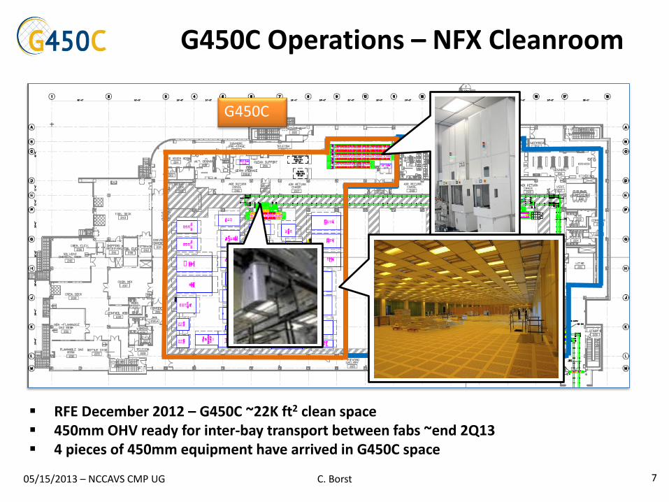
G450C Operations – NFX Cleanroom
RFE December 2012 – G450C ~22K ft2 clean space 450mm OHV ready for inter-bay transport between fabs ~end 2Q13 4 pieces of 450mm equipment have arrived in G450C space
05/15/2013 – NCCAVS CMP UG C. Borst 7
G450C

Equipment Performance Metrics (EPM)
• G450C will evaluate CMP equipment versus the current published Equipment Performance Metrics (EPM)
• The EPM: – was built with inputs from all G450C member companies – Targets the 14nm node
Priorities among the many attributes included in the EPM are generally as follows: • Process performance, including defectivity, is a baseline requirement; it
must be at 450mm as good as or better than that for the equivalent 300mm tools
• 450 mm tool productivity must be as good as or better than 300mm tools on a per-wafer basis for the same tool configuration by the time of HVM.
• Other components of performance such as batch size, process control, MTBF, etc. must be optimized to achieve the two overarching goals above
05/15/2013 – NCCAVS CMP UG C. Borst 8
www.g450c.org

CMP EPM - Oxide
SOBT3 = same or better than 300mm tool
05/15/2013 – NCCAVS CMP UG C. Borst 9

CMP EPM – Oxide (continued)
05/15/2013 – NCCAVS CMP UG C. Borst 10

Consumables Directions for 450mm
What may drive CMP consumable differences for 450mm equipment?
• Revisit the EPM: – 14nm node – Equivalent process performance to 300 – Equivalent equipment productivity to 300 – Edge exclusion 1.5mm – Equivalent normalized throughput
• Assume the probability of equipment configuration change due to size increase (2 platens)
• Assume that requirements of process/equipment yield for 450mm will drive CMP control improvements – (Wafer scrap hurts 2.25x as much)
05/15/2013 – NCCAVS CMP UG C. Borst 11

Consumables Directions for 450mm - Slurry
Slurry suppliers must work with equipment suppliers to co-develop / optimize slurry sets for larger wafers, while keeping flow rates reasonable
• Improvement of slurry stability / manufacturing tolerances – 14nm node requires lower defectivity; tighter particle size control – Better stability within drum, local reservoir, and slurry loop – Compatibility with inline or loop filtration (higher flow rates, more
susceptible to shear) – Successful and stable dilution in sub-fab and on-platen
• On-platen mixing – Two-platen designs could drive higher instance of ‘high rate and soft-
landing’ slurries on one platen – ‘Slurry sets’ with ensured compatibility could be much more important
05/15/2013 – NCCAVS CMP UG C. Borst 12

Consumables Directions for 450mm - Pad
Pad development for >40 inch platen must continue along (and expand upon) recent advancing trends
• Optimization of pad materials and groove configuration – to complement 14nm node advanced slurry engineering – to maximize performance with larger wafers – to further enable efficient on-platen slurry mixing or transition
• Uniformity of pad material properties – across pad (larger area, larger wafer contact area) – pad-to-pad (single-cast or batch uniformity controls)
• Maintain compatibility with improving process control / endpoint systems
05/15/2013 – NCCAVS CMP UG C. Borst 13

Consumables Directions for 450mm - Disk
Diamond conditioning, and other modes of pad refreshing or cleaning, increase in importance for >40 inch platens
• Platen size could drive disk changes – larger disks, and/or multiple disks per pad – better control / predictability at higher pressures may be required to
maintain through-life pad performance
• Platen size increase would benefit from improved ‘conditioner efficiency’ – higher slurry flow rates, larger slurry ‘capture area’ under wafer – developing a better disk, the physics of which are better understood, that
complements pad cleaning may have differentiating advantages
05/15/2013 – NCCAVS CMP UG C. Borst 14

Summary G450C’s mission is to evaluate equipment capability versus the EPM specification – which begins with demonstration of the supplier-selected BKM at the 14nm node
The certainties: • Wafer and pad get bigger, and process/equipment scrap frequency must reduce • IDMs require zero performance degradation vs 300mm (including defectivity)
and are pushing aggressive targets to consumable consumption rates
The assumptions: • Slurry flow rate increases (probably belongs above) • Two-platen configurations will be more prevalent
The projections: • Consumable manufacture, and performance during process, will require tighter
tolerances (slurry, pad, and disk) • On-platen slurry mixing may become more prevalent • Pad properties and grooving must be optimized to slurry set
450mm CMP tools are available now at supplier labs, and will be available to G450C starting 2H13 – results will confirm/refute projections and highlight new challenges 05/15/2013 – NCCAVS CMP UG C. Borst 15