cmt2219a gnd xin 960 mhz ook/(g)fsk receiveren)-rev1.0.pdf · 300 – 960 mhz ook/(g)fsk receiver...
TRANSCRIPT
CMT2219A
Rev 1.0 | Page 1/40
www.cmostek.com
CMT2219A 300 – 960 MHz OOK/(G)FSK Receiver
Copyright © By CMOSTEK
Features
Optional Chip Feature Configuration Schemes
On-Line Registers Configuration
Off-Line EEPROM Programming
Frequency Range: 300 to 960 MHz
FSK, GFSK and OOK Demodulation
Symbol Rate: 0.1 to 100 ksps
Sensitivity: -109 dBm @ 9.6 ksps, FSK, 868.35 MHz
4-wire SPI Interface
Direct, Buffer and Packet Mode Supported
Configurable Data Handler and 32-Byte FIFO
Manchester Decoding and Data De-Whitening
Supply Voltage: 1.8 to 3.6 V
Low Power Consumption: 5.7 mA
Low Sleep Current
60 nA when Sleep Timer Off
440 nA when Sleep Timer On
RoHS Compliant
16-pin QFN 3x3 Package
Applications
Low-Cost Consumer Electronics Applications
Home and Building Automation
Infrared Receiver Replacements
Industrial Monitoring and Controls
Remote Automated Meter Reading
Remote Lighting Control System
Wireless Alarm and Security Systems
Remote Keyless Entry (RKE)
Ordering Information
Part Number Frequency Package MOQ
CMT2219A-EQR 868.35 MHz QFN16 5,000 pcs
More Ordering Info: See Page35
Descriptions
The CMT2219A is an ultra low power, high performance,
OOK and (G)FSK receiver for various 300 to 960 MHz
wireless applications. It is part of the CMOSTEK
NextGenRFTM family, which includes a complete line of
transmitters, receivers and transceivers. All features can be
configured either by off-line EEPROM programming or
on-line registers writing. The configuration file to be written
into the registers is generated by the smart RFPDK. The
CMT2219A operates from a supply voltage of 1.8 V to 3.6
V, when it is always on, it consumes only 5.7 mA current
while achieving -109 dBm receiving sensitivity (FSK, 9.6
ksps symbol rate, 868.35 MHz), and only 60 nA sleep
current for superior battery life. The device supports packet
handling, 32-byte FIFO, Manchester decoding and data
de-whitening for the received data processing. Besides the
demodulated data and the sync clock, the device can also
send out the power-on reset, the system clock, as well as 2
configurable interrupts for the external device. CMT2219A
receiver together with the CMT211xA transmitter enables a
powerful RF link.
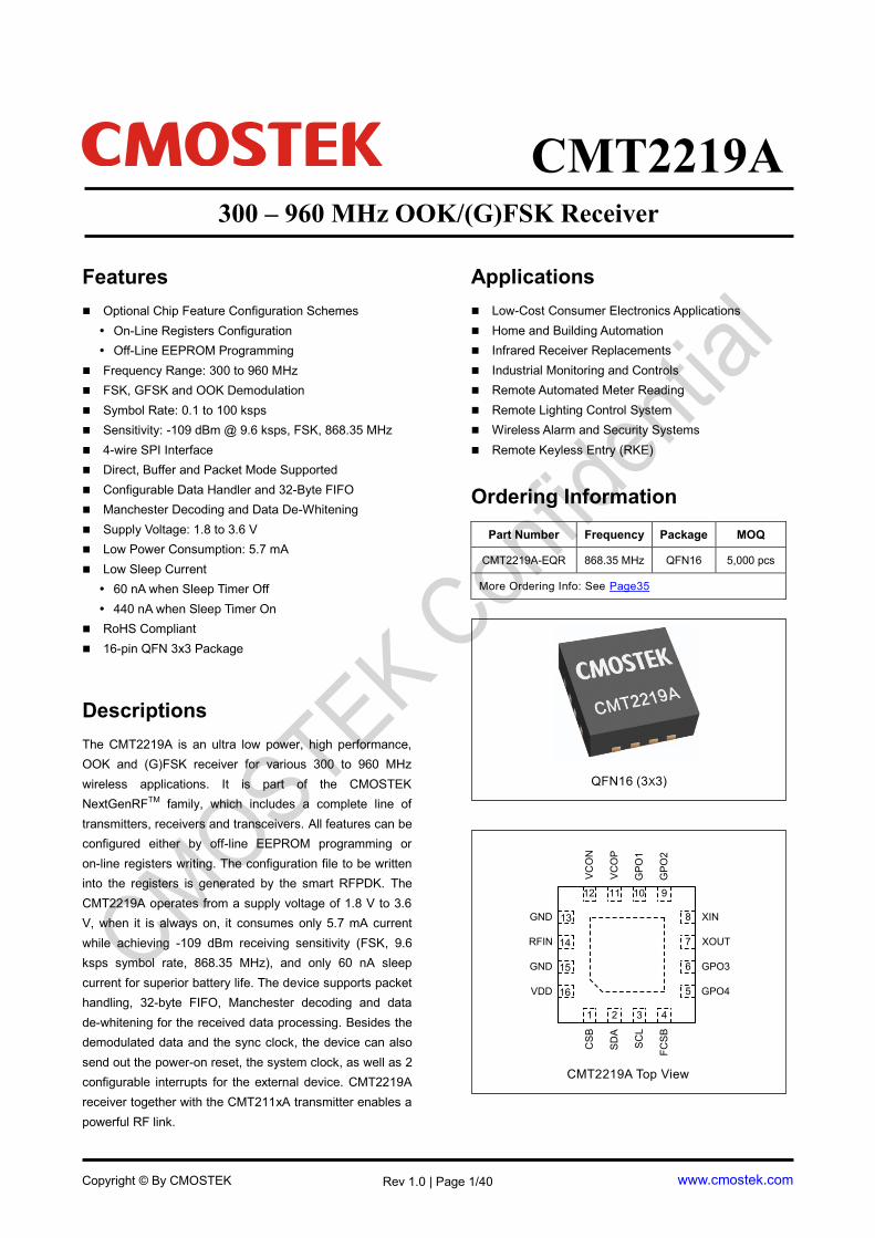
QFN16 (3X3)
GND
RFIN
GND
VDD
CS
B
SD
A
SC
L
FC
SB
XIN
XOUT
GPO3
GPO4
VC
ON
VC
OP
GP
O1
GP
O2
13
14
15
16
1 2 3 4
5
6
7
8
9101112
CMT2219A Top View
CMT2219A
Rev 1.0 | Page 2/40
www.cmostek.com
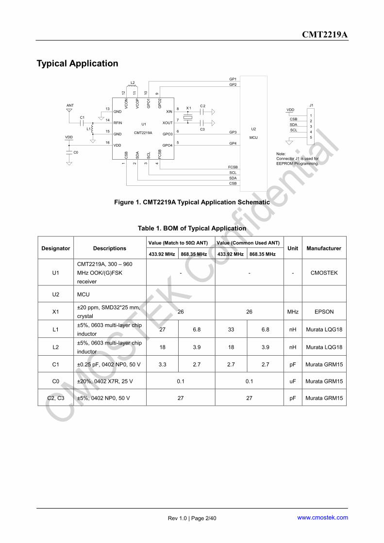
Typical Application
U1
CMT2219A
XIN
XOUT
GPO3
GPO4
GP
O2
GP
O1
VC
OP
VC
ON
GND
RFIN
GND
CS
B
SD
A
SC
L
FC
SB
VDD
L1
C1
C0
ANT13
14
15
16
910
11
12
5
6
7
8C 2
X 1
1 2 3 4
L2
C3
VDD
U2
MCU
GP1
GP2
GP3
GP4
FCSB
SCL
SDA
CSB
Note:
Connector J1 is used for
EEPROM Programming.
VDD
J1
1
2
3
4
5
CSB
SDA
SCL
Figure 1. CMT2219A Typical Application Schematic
Table 1. BOM of Typical Application
Designator Descriptions Value (Match to 50Ω ANT) Value (Common Used ANT)
Unit Manufacturer 433.92 MHz 868.35 MHz 433.92 MHz 868.35 MHz
U1
CMT2219A, 300 – 960
MHz OOK/(G)FSK
receiver
- - - CMOSTEK
U2 MCU
X1 ±20 ppm, SMD32*25 mm,
crystal 26 26 MHz EPSON
L1 ±5%, 0603 multi-layer chip
inductor 27 6.8 33 6.8 nH Murata LQG18
L2 ±5%, 0603 multi-layer chip
inductor 18 3.9 18 3.9 nH Murata LQG18
C1 ±0.25 pF, 0402 NP0, 50 V 3.3 2.7 2.7 2.7 pF Murata GRM15
C0 ±20%, 0402 X7R, 25 V 0.1 0.1 uF Murata GRM15
C2, C3 ±5%, 0402 NP0, 50 V 27 27 pF Murata GRM15

CMT2219A
Rev 1.0 | Page 3/40
www.cmostek.com
Abbreviations
Abbreviations used in this data sheet are described below.
ADC Analog to Digital Converter NP0 Negative-Positive-Zero
AFC Automatic-Frequency-Control NC Not Connected
AGC Automatic Gain Control OOK On-Off Keying
AN Application Notes PC Personal Computer
BER Bit Error Rate PCB Printed Circuit Board
BOM Bill of Materials PLL Phase Lock Loop
BSC Basic Spacing between Centers PN9 Pseudorandom Noise 9
BT bandwidth-time product POR Power On Reset
BW Bandwidth PUP Power Up
CRC
DC
Cyclic Redundancy Check
Direct Current
QFN Quad Flat No-lead
RESV Reserved
EEPROM Electrically Erasable Programmable Read-Only
Memory
RF Radio Frequency
RFPDK RF Products Development Kit
ESD Electro-Static Discharge RoHS Restriction of Hazardous Substances
ESR Equivalent Series Resistance RSSI Received Signal Strength Indicator
Ext Extended Rx Receiving, Receiver
FIFO First In First Out SAR Successive Approximation Register
FSK Frequency-Shift Keying SMD Surface Mounted Devices
GFSK Gauss frequency Shift Keying SPI Serial Port Interface
GPO General Purpose Output SR Symbol Rate
HEX Hexadecimal STBY Standby
IF Intermediate Frequency TH Threshold
LNA Low Noise Amplifier Tx Transmission, Transmitter
LO Local Oscillator Typ Typical
LPOSC Low Power Oscillator USB Universal Serial Bus
Max Maximum VCO Voltage Controlled Oscillator
MCU Microcontroller Unit WOR Wake-On Radio
Min Minimum XOSC Crystal Oscillator
MOQ Minimum Order Quantity XTAL/Xtal Crystal
NA Not Applicable/Not Available

CMT2219A
Rev 1.0 | Page 4/40
www.cmostek.com
Table of Contents
1. Electrical Characteristics ............................................................................................................................................ 6
1.1 Recommended Operation Conditions ................................................................................................................... 6
1.2 Absolute Maximum Ratings................................................................................................................................... 6
1.3 Receiver Specifications ......................................................................................................................................... 7
1.4 Crystal Oscillator ................................................................................................................................................... 8
1.5 LPOSC .................................................................................................................................................................. 8
2. Pin Descriptions .......................................................................................................................................................... 9
3. Typical Performance Characteristics ....................................................................................................................... 10
4. Typical Application Schematic ................................................................................................................................. 11
5. Functional Descriptions ............................................................................................................................................ 12
5.1 Overview ............................................................................................................................................................. 12
5.2 Modulation, Frequency and Symbol Rate ........................................................................................................... 12
5.3 Embedded EEPROM and RFPDK ...................................................................................................................... 13
5.4 All Configurable Options ..................................................................................................................................... 13
5.5 Internal Blocks Description .................................................................................................................................. 17
5.5.1 RF Front-end and AGC ............................................................................................................................ 17
5.5.2 IF Filter ..................................................................................................................................................... 17
5.5.3 RSSI ........................................................................................................................................................ 17
5.5.4 SAR ADC ................................................................................................................................................. 17
5.5.5 Crystal Oscillator ...................................................................................................................................... 17
5.5.6 Frequency Synthesizer ............................................................................................................................ 18
5.5.7 LPOSC ..................................................................................................................................................... 18
5.5.8 OOK Demodulation .................................................................................................................................. 18
5.5.9 (G)FSK Demodulation .............................................................................................................................. 18
5.6 SPI Interface ....................................................................................................................................................... 19
5.6.1 Register Read & Write Operation ............................................................................................................. 19
5.6.2 FIFO Read Operation .............................................................................................................................. 20
5.7 Operation States, Timing and Power .................................................................................................................. 21
5.7.1 Power-Up Sequence ................................................................................................................................ 21
5.7.2 Operating States ...................................................................................................................................... 21
5.8 GPOs and Interrupts ........................................................................................................................................... 23
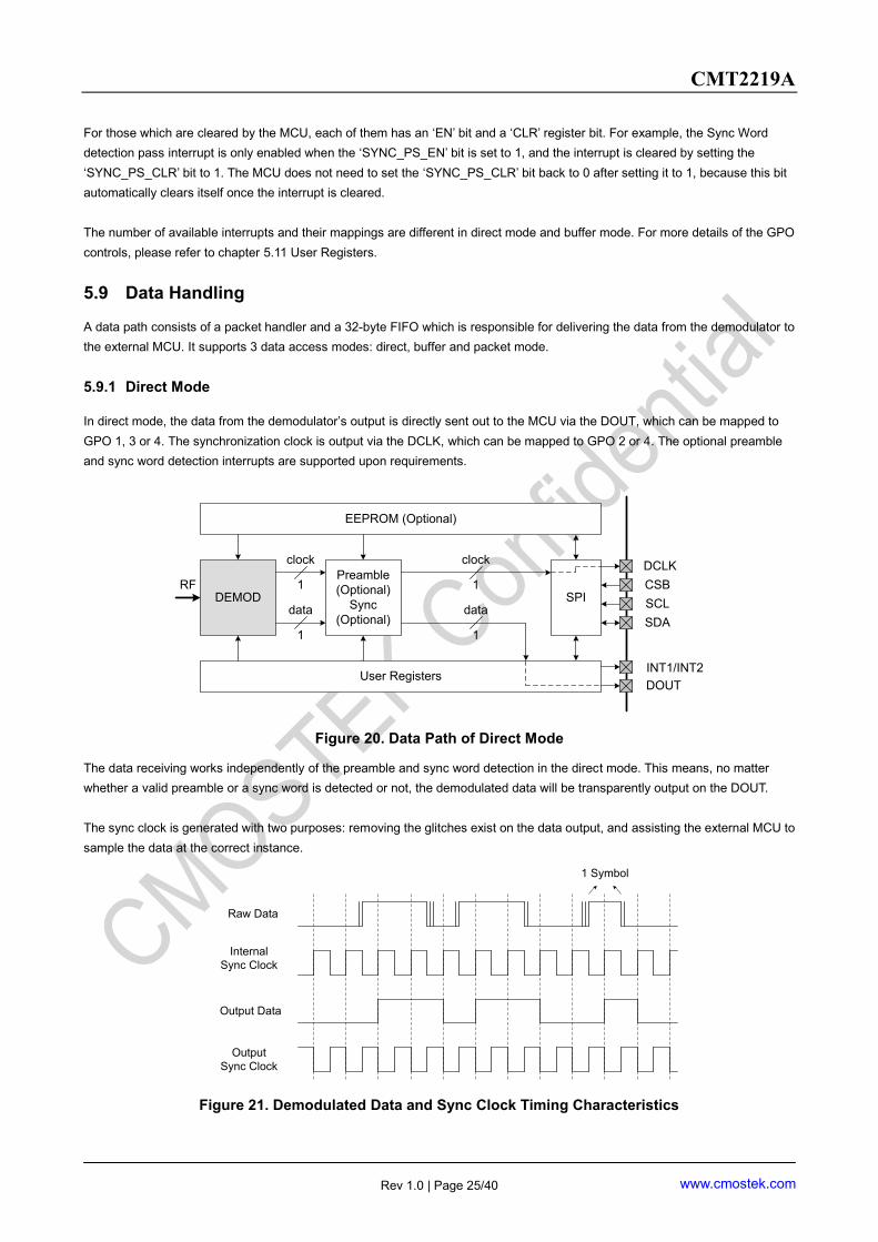
5.9 Data Handling ..................................................................................................................................................... 25
5.9.1 Direct Mode ............................................................................................................................................. 25
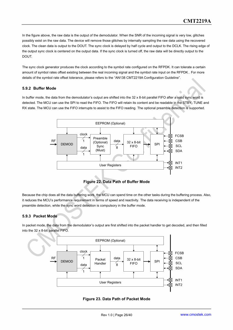
5.9.2 Buffer Mode ............................................................................................................................................. 26
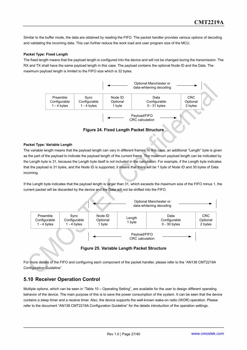
5.9.3 Packet Mode ............................................................................................................................................ 26
5.10 Receiver Operation Control ................................................................................................................................. 27
5.11 User Registers .................................................................................................................................................... 28
5.11.1 Configuration Bank .................................................................................................................................. 28
5.11.2 Control Bank ............................................................................................................................................ 28
6. Ordering Information ................................................................................................................................................. 35
7. Package Outline ......................................................................................................................................................... 36
CMT2219A
Rev 1.0 | Page 5/40
www.cmostek.com
8. Top Marking ............................................................................................................................................................... 37
8.1 CMT2219A Top Marking ..................................................................................................................................... 37
9. Other Documentations .............................................................................................................................................. 38
10. Document Change List.............................................................................................................................................. 39
11. Contact Information .................................................................................................................................................. 40
CMT2219A
Rev 1.0 | Page 6/40
www.cmostek.com
1. Electrical Characteristics
VDD = 3.3 V, TOP = 25 ℃, FRF = 868.35 MHz, sensitivities are measured in receiving a PN9 sequence and matching to 50 Ω
impedance, with the BER of 0.1%. All measurements are performed using the board CMT2219A-EM V1.0, unless otherwise
noted.
1.1 Recommended Operation Conditions
Table 2. Recommended Operation Conditions
Parameter Symbol Conditions Min Typ Max Unit
Operation Voltage Supply VDD 1.8 3.6 V
Operation Temperature TOP -40 85 ℃
Supply Voltage Slew Rate 1 mV/us
1.2 Absolute Maximum Ratings
Table 3. Absolute Maximum Ratings[1]
Parameter Symbol Conditions Min Max Unit
Supply Voltage VDD -0.3 3.6 V
Interface Voltage VIN -0.3 VDD + 0.3 V
Junction Temperature TJ -40 125 ℃
Storage Temperature TSTG -50 150 ℃
Soldering Temperature TSDR Lasts at least 30 seconds 255 ℃
ESD Rating[2] Human Body Model (HBM) -2 2 kV
Latch-up Current @ 85 ℃ -100 100 mA
Notes:
[1]. Stresses above those listed as “absolute maximum ratings” may cause permanent damage to the device. This is a stress
rating only and functional operation of the device under these conditions is not implied. Exposure to maximum rating
conditions for extended periods may affect device reliability.
[2]. The CMT2219A is high-performance RF integrated circuits with VCON/P pins having an ESD rating < 2 kV HBM.
Handling and assembly of this device should only be done at ESD-protected workstations.
Caution! ESD sensitive device. Precaution should be used when handling the device in order
to prevent permanent damage.
CMT2219A
Rev 1.0 | Page 7/40
www.cmostek.com
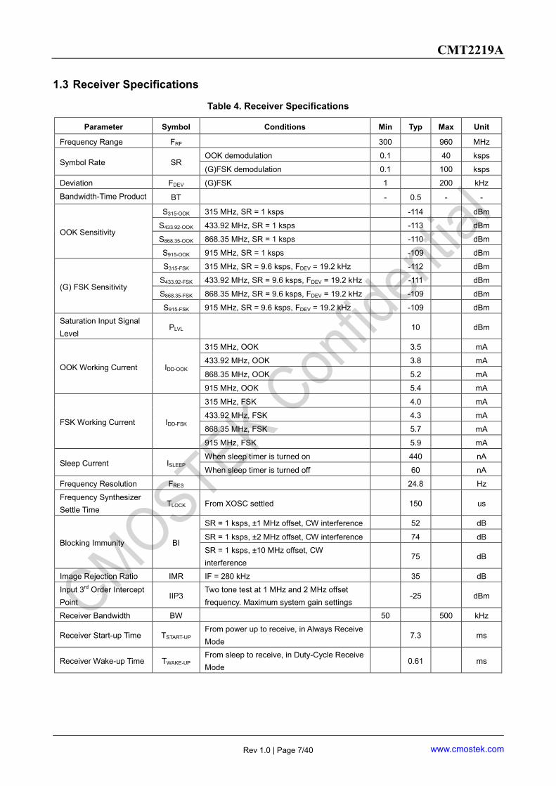
1.3 Receiver Specifications
Table 4. Receiver Specifications
Parameter Symbol Conditions Min Typ Max Unit
Frequency Range FRF 300 960 MHz
Symbol Rate SR
OOK demodulation 0.1 40 ksps
(G)FSK demodulation 0.1 100 ksps
Deviation FDEV (G)FSK 1 200 kHz
Bandwidth-Time Product BT - 0.5 - -
OOK Sensitivity
S315-OOK 315 MHz, SR = 1 ksps -114 dBm
S433.92-OOK 433.92 MHz, SR = 1 ksps -113 dBm
S868.35-OOK 868.35 MHz, SR = 1 ksps -110 dBm
S915-OOK 915 MHz, SR = 1 ksps -109 dBm
(G) FSK Sensitivity
S315-FSK 315 MHz, SR = 9.6 ksps, FDEV = 19.2 kHz -112 dBm
S433.92-FSK 433.92 MHz, SR = 9.6 ksps, FDEV = 19.2 kHz -111 dBm
S868.35-FSK 868.35 MHz, SR = 9.6 ksps, FDEV = 19.2 kHz -109 dBm
S915-FSK 915 MHz, SR = 9.6 ksps, FDEV = 19.2 kHz -109 dBm
Saturation Input Signal
Level PLVL 10 dBm
OOK Working Current IDD-OOK
315 MHz, OOK 3.5 mA
433.92 MHz, OOK 3.8 mA
868.35 MHz, OOK 5.2 mA
915 MHz, OOK 5.4 mA
FSK Working Current IDD-FSK
315 MHz, FSK 4.0 mA
433.92 MHz, FSK 4.3 mA
868.35 MHz, FSK 5.7 mA
915 MHz, FSK 5.9 mA
Sleep Current ISLEEP
When sleep timer is turned on 440 nA
When sleep timer is turned off 60 nA
Frequency Resolution FRES 24.8 Hz
Frequency Synthesizer
Settle Time TLOCK From XOSC settled 150 us
Blocking Immunity BI
SR = 1 ksps, ±1 MHz offset, CW interference 52 dB
SR = 1 ksps, ±2 MHz offset, CW interference 74 dB
SR = 1 ksps, ±10 MHz offset, CW
interference 75 dB
Image Rejection Ratio IMR IF = 280 kHz 35 dB
Input 3rd Order Intercept
Point IIP3
Two tone test at 1 MHz and 2 MHz offset
frequency. Maximum system gain settings -25 dBm
Receiver Bandwidth BW 50 500 kHz
Receiver Start-up Time TSTART-UP From power up to receive, in Always Receive
Mode 7.3 ms
Receiver Wake-up Time TWAKE-UP From sleep to receive, in Duty-Cycle Receive
Mode 0.61 ms
CMT2219A
Rev 1.0 | Page 8/40
www.cmostek.com
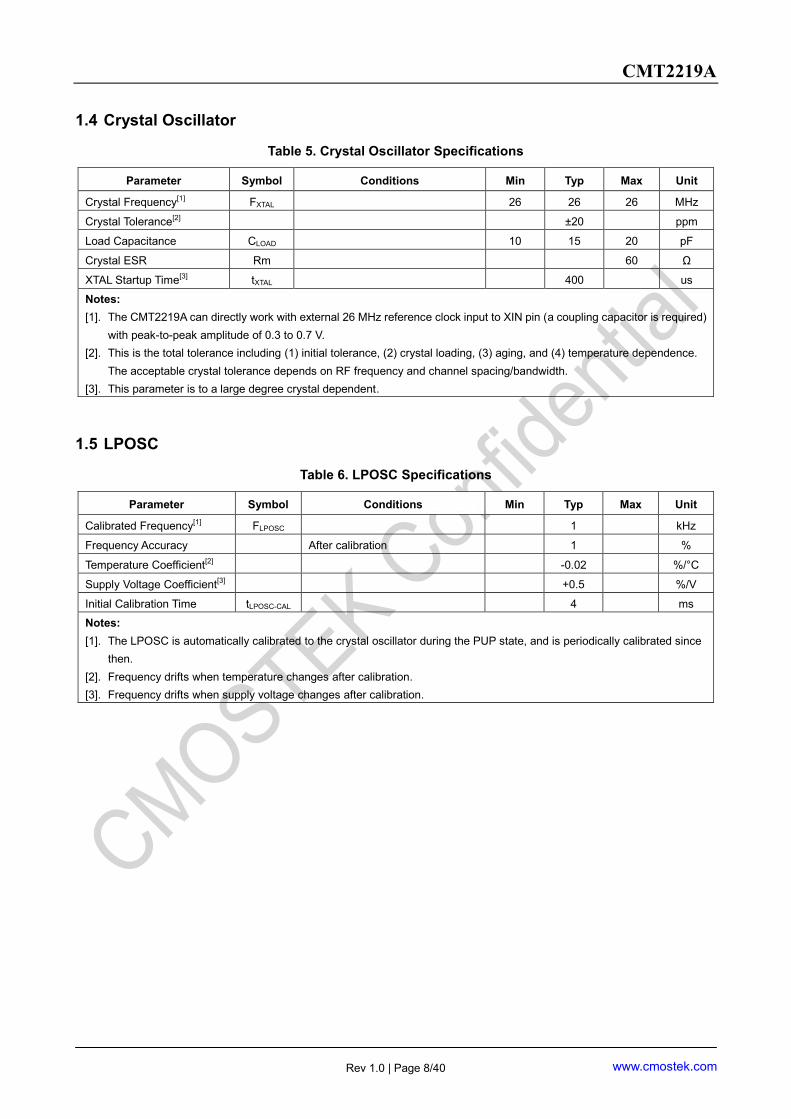
1.4 Crystal Oscillator
Table 5. Crystal Oscillator Specifications
Parameter Symbol Conditions Min Typ Max Unit
Crystal Frequency[1] FXTAL 26 26 26 MHz
Crystal Tolerance[2] ±20 ppm
Load Capacitance CLOAD 10 15 20 pF
Crystal ESR Rm 60 Ω
XTAL Startup Time[3] tXTAL 400 us
Notes:
[1]. The CMT2219A can directly work with external 26 MHz reference clock input to XIN pin (a coupling capacitor is required)
with peak-to-peak amplitude of 0.3 to 0.7 V.
[2]. This is the total tolerance including (1) initial tolerance, (2) crystal loading, (3) aging, and (4) temperature dependence.
The acceptable crystal tolerance depends on RF frequency and channel spacing/bandwidth.
[3]. This parameter is to a large degree crystal dependent.
1.5 LPOSC
Table 6. LPOSC Specifications
Parameter Symbol Conditions Min Typ Max Unit
Calibrated Frequency[1] FLPOSC 1 kHz
Frequency Accuracy After calibration 1 %
Temperature Coefficient[2] -0.02 %/°C
Supply Voltage Coefficient[3] +0.5 %/V
Initial Calibration Time tLPOSC-CAL 4 ms
Notes:
[1]. The LPOSC is automatically calibrated to the crystal oscillator during the PUP state, and is periodically calibrated since
then.
[2]. Frequency drifts when temperature changes after calibration.
[3]. Frequency drifts when supply voltage changes after calibration.
CMT2219A
Rev 1.0 | Page 9/40
www.cmostek.com
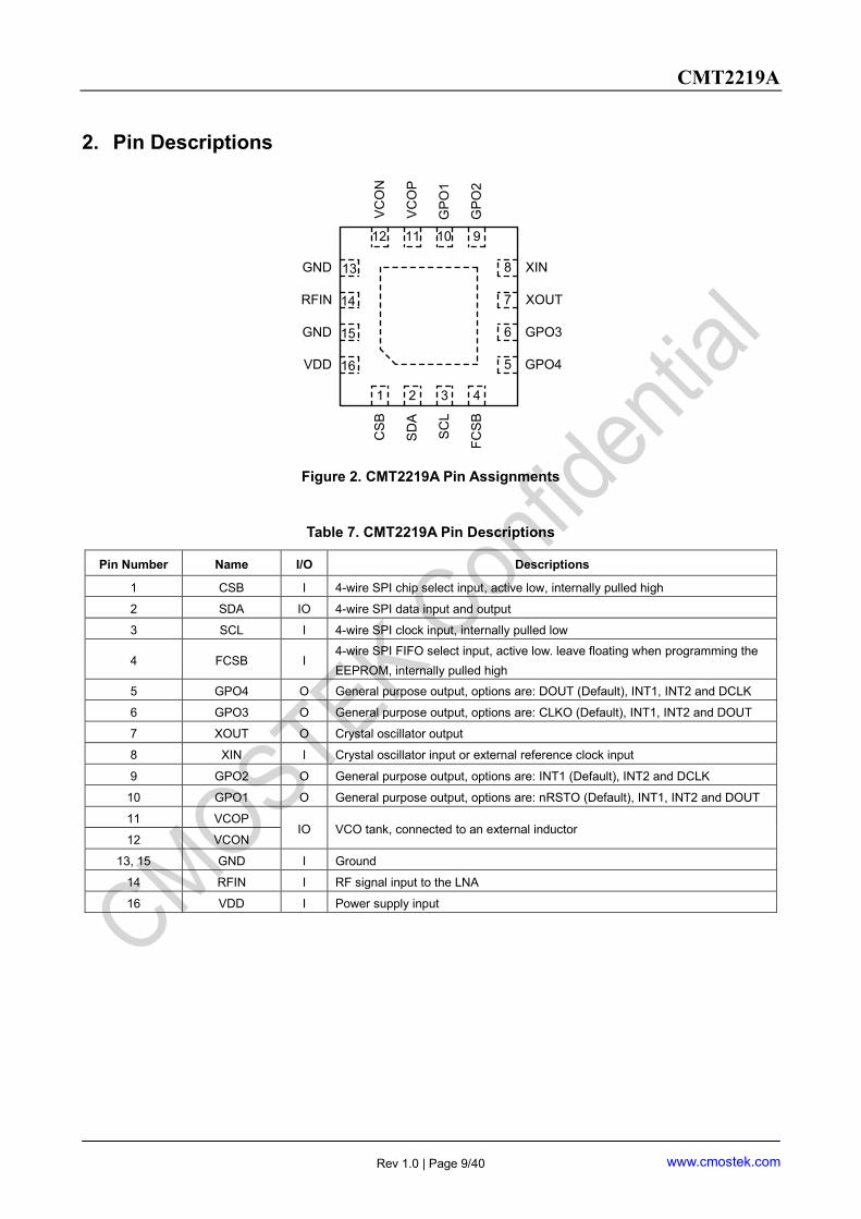
2. Pin Descriptions
GND
RFIN
GND
VDDC
SB
SD
A
SC
L
FC
SB
XIN
XOUT
GPO3
GPO4V
CO
N
VC
OP
GP
O1
GP
O2
13
14
15
16
1 2 3 4
5
6
7
8
9101112
Figure 2. CMT2219A Pin Assignments
Table 7. CMT2219A Pin Descriptions
Pin Number Name I/O Descriptions
1 CSB I 4-wire SPI chip select input, active low, internally pulled high
2 SDA IO 4-wire SPI data input and output
3 SCL I 4-wire SPI clock input, internally pulled low
4 FCSB I 4-wire SPI FIFO select input, active low. leave floating when programming the
EEPROM, internally pulled high
5 GPO4 O General purpose output, options are: DOUT (Default), INT1, INT2 and DCLK
6 GPO3 O General purpose output, options are: CLKO (Default), INT1, INT2 and DOUT
7 XOUT O Crystal oscillator output
8 XIN I Crystal oscillator input or external reference clock input
9 GPO2 O General purpose output, options are: INT1 (Default), INT2 and DCLK
10 GPO1 O General purpose output, options are: nRSTO (Default), INT1, INT2 and DOUT
11 VCOP IO VCO tank, connected to an external inductor
12 VCON
13, 15 GND I Ground
14 RFIN I RF signal input to the LNA
16 VDD I Power supply input

CMT2219A
Rev 1.0 | Page 10/40
www.cmostek.com
3. Typical Performance Characteristics
2.00
2.50
3.00
3.50
4.00
4.50
5.00
5.50
6.00
1.60 1.85 2.10 2.35 2.60 2.85 3.10 3.35 3.60 3.85
Cu
rren
t C
on
su
mp
tio
n (
mA
)
Supply Voltage (V)
Current vs. Supply Voltage
868.35 MHz
433.92 MHz
3.40
3.80
4.20
4.60
5.00
5.40
5.80
6.20
6.60
-50 -30 -10 10 30 50 70 90
Cu
rre
nt C
on
su
mp
tio
n (
mA)
Temperature (℃)
Current vs. Temperature
868.35MHz/3.6V
868.35MHz/3.3V
868.35MHz/1.8V
433.92MHz/3.6V
433.92MHz/3.3V
433.92MHz/1.8V
-115.0
-114.0
-113.0
-112.0
-111.0
-110.0
-109.0
-108.0
-107.0
1.6 1.9 2.2 2.5 2.8 3.1 3.4 3.7 4
Sen
sit
ivit
y (
dB
m)
Supply Voltage (V)
Sensitivity vs. Supply Voltage
868.35 MHz
433.92 MHz
-114
-113
-112
-111
-110
-109
-108
-50 -30 -10 10 30 50 70 90
Se
ns
itiv
ity
(d
Bm
)
Temperature (℃)
Sensitivity vs. Temperature
868.35 MHz
433.92 MHz
-120
-115
-110
-105
-100
-95
-90
0 5 10 15 20 25 30 35 40
Se
ns
itiv
ity
(d
Bm
)
Symbol Rate (ksps)
Sensitivity vs. Symbol Rate
868.35 MHz
433.92 MHz
-115
-114
-113
-112
-111
-110
-109
-108
0.01% 0.10% 1.00% 10.00%
Se
ns
itiv
ity
(d
Bm
)
Bit Error Rate
Sensitivity vs. BER
868.35 MHz
433.92 MHz
Figure 3. Current vs. Voltage, FRF = 433.92 /
868.35 MHz, OOK, SR = 1 ksps
Figure 8. Sensitivity vs. BER, FRF = 433.92 /
868.35 MHz, VDD = 3.3 V, SR = 1 ksps
Figure 4. Current vs. Temperature, FRF =
433.92 / 868.35 MHz, FSK, SR = 1 ksps
Figure 5. Sensitivity vs. Supply Voltage, SR
= 1 ksps, OOK, BER = 0.1%
Figure 7. Sensitivity vs. SR, FRF = 433.92 /
868.35 MHz, OOK, VDD = 3.3 V, BER = 0.1%
Figure 6. Sensitivity vs. Temperature, FRF = 433.92 /
868.35 MHz, FSK, VDD = 3.3 V, SR = 1 ksps, BER = 0.1%

CMT2219A
Rev 1.0 | Page 11/40
www.cmostek.com
4. Typical Application Schematic
U1
CMT2219A
XIN
XOUT
GPO3
GPO4
GP
O2
GP
O1
VC
OP
VC
ON
GND
RFIN
GND
CS
B
SD
A
SC
L
FC
SB
VDD
L1
C1
C0
ANT13
14
15
16
910
11
12
5
6
7
8C 2
X 1
1 2 3 4
L2
C3
VDD
U2
MCU
GP1
GP2
GP3
GP4
FCSB
SCL
SDA
CSB
Note:
Connector J1 is used for
EEPROM Programming.
VDD
J1
1
2
3
4
5
CSB
SDA
SCL
Figure 9. Typical Application Schematic
Notes:
1. Connector J1 is a must for the CMT2219A EEPROM access during development or manufacture stage.
2. The general layout guidelines are listed below. For more design details, please refer to “AN107 CMT221x Schematic and
PCB Layout Design Guideline”.
Use as much continuous ground plane metallization as possible.
Use as many grounding vias (especially near to the GND pins) as possible to minimize series parasitic inductance
between the ground pour and the GND pins.
Avoid using long and/or thin transmission lines to connect the components.
Place C0 as close to the CMT2219A as possible for better filtering.
3. The table below shows the BOM of typical application.
Table 8. BOM of Typical Application
Designator Descriptions Value (Match to 50Ω ANT) Value (Common Used ANT)
Unit Manufacturer 433.92 MHz 868.35 MHz 433.92 MHz 868.35 MHz
U1
CMT2219A, 300 – 960
MHz OOK/(G)FSK
receiver
- - - CMOSTEK
U2 MCU
X1 ±20 ppm, SMD32*25 mm,
crystal 26 26 MHz EPSON
L1 ±5%, 0603 multi-layer chip
inductor 27 6.8 33 6.8 nH Murata LQG18
L2 ±5%, 0603 multi-layer chip
inductor 18 3.9 18 3.9 nH Murata LQG18
C1 ±0.25 pF, 0402 NP0, 50 V 3.3 2.7 2.7 2.7 pF Murata GRM15
C0 ±20%, 0402 X7R, 25 V 0.1 0.1 uF Murata GRM15
C2, C3 ±5%, 0402 NP0, 50 V 27 27 pF Murata GRM15
CMT2219A
Rev 1.0 | Page 12/40
www.cmostek.com
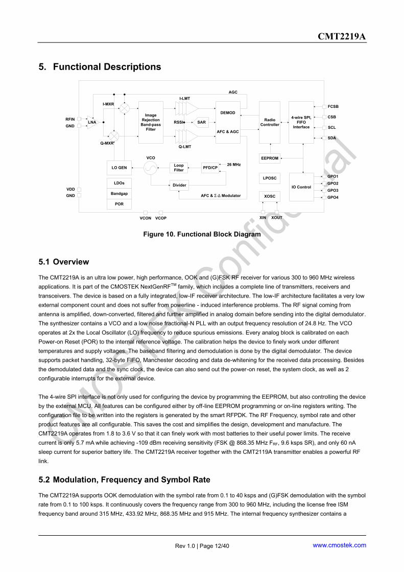
5. Functional Descriptions
Image
Rejection
Band-pass
Filter
DEMOD
AFC & AGC
LO GEN
AGC
Radio
ControllerLNA
IO Control
XOSCBandgap
I-LMT
Q-LMT
I-MXR
Q-MXR
SAR
POR
RSSIRFIN
GND
Loop
Filter
Divider
AFC & Σ-Δ Modulator
26 MHz
VCON VCOP XIN XOUT
CSB
SCL
SDA
LDOs
VCO
PFD/CP
VDD
GND
4-wire SPI,
FIFO
Interface
LPOSC
FCSB
EEPROM
GPO2
GPO3
GPO4
GPO1
Figure 10. Functional Block Diagram
5.1 Overview
The CMT2219A is an ultra low power, high performance, OOK and (G)FSK RF receiver for various 300 to 960 MHz wireless
applications. It is part of the CMOSTEK NextGenRFTM family, which includes a complete line of transmitters, receivers and
transceivers. The device is based on a fully integrated, low-IF receiver architecture. The low-IF architecture facilitates a very low
external component count and does not suffer from powerline - induced interference problems. The RF signal coming from
antenna is amplified, down-converted, filtered and further amplified in analog domain before sending into the digital demodulator.
The synthesizer contains a VCO and a low noise fractional-N PLL with an output frequency resolution of 24.8 Hz. The VCO
operates at 2x the Local Oscillator (LO) frequency to reduce spurious emissions. Every analog block is calibrated on each
Power-on Reset (POR) to the internal reference voltage. The calibration helps the device to finely work under different
temperatures and supply voltages. The baseband filtering and demodulation is done by the digital demodulator. The device
supports packet handling, 32-byte FIFO, Manchester decoding and data de-whitening for the received data processing. Besides
the demodulated data and the sync clock, the device can also send out the power-on reset, the system clock, as well as 2
configurable interrupts for the external device.
The 4-wire SPI interface is not only used for configuring the device by programming the EEPROM, but also controlling the device
by the external MCU. All features can be configured either by off-line EEPROM programming or on-line registers writing. The
configuration file to be written into the registers is generated by the smart RFPDK. The RF Frequency, symbol rate and other
product features are all configurable. This saves the cost and simplifies the design, development and manufacture. The
CMT2219A operates from 1.8 to 3.6 V so that it can finely work with most batteries to their useful power limits. The receive
current is only 5.7 mA while achieving -109 dBm receiving sensitivity (FSK @ 868.35 MHz FRF, 9.6 ksps SR), and only 60 nA
sleep current for superior battery life. The CMT2219A receiver together with the CMT2119A transmitter enables a powerful RF
link.
5.2 Modulation, Frequency and Symbol Rate
The CMT2219A supports OOK demodulation with the symbol rate from 0.1 to 40 ksps and (G)FSK demodulation with the symbol
rate from 0.1 to 100 ksps. It continuously covers the frequency range from 300 to 960 MHz, including the license free ISM
frequency band around 315 MHz, 433.92 MHz, 868.35 MHz and 915 MHz. The internal frequency synthesizer contains a

CMT2219A
Rev 1.0 | Page 13/40
www.cmostek.com
high-purity VCO and a low noise fractional-N PLL with an output frequency resolution of 24.8 Hz. See the table below for the
demodulation, frequency and symbol rate information.
Table 9. Modulation, Frequency and Symbol Rate
Parameter Value Unit
Demodulation OOK, FSK and GFSK -
Frequency 300 to 960 MHz
Frequency Resolution 24.8 Hz
Symbol Rate OOK: 0.1 to 40 ksps
(G)FSK: 0.1 to 100 ksps
5.3 Embedded EEPROM and RFPDK
The RFPDK is a PC application developed to help the user to configure the CMOSTEK NextGenRFTM products in the most
intuitional way. The user only needs to connect the USB Programmer between the PC and the device, fill in/select the proper
value of each parameter on the RFPDK, and click the “Burn” button to program the configurations into the device. The
configurations of the device will then remain unchanged until the next programming. No external MCU control is required in the
application program.
The RFPDK also allows the user to save the active configuration into a list by clicking on the “List” button, so that the saved
configuration can be directly reloaded from the list in the future. Furthermore, it supports exporting the configuration into a
hexadecimal file by clicking on the “Export” button. This file can be used to burn the same configuration into a large amount of
devices during the mass production, or used as an HEX file to load into the external MCU program for on-line configuration using
registers. See the figure below for the accessing of the EEPROM.
CMT2219A
InterfaceCMOSTEK USB
Programmer
SCL
SDA
RFPDK
EEPROM
CSB
Figure 11. Accessing Embedded EEPROM
For more details of the CMOSTEK USB Programmer and the RFPDK, please refer to “AN103 CMT211xA-221xA One-Way RF
Link Development Kits Users Guide”.
5.4 All Configurable Options
Besides the demodulation, frequency and symbol rate, more options can be used to customize the device. The following is a
table of all the configurable options. On the RFPDK, the Basic Mode only contains a few options allowing the user to perform
easy and fast configurations. The Advanced Mode shows all the options that allow the user to customize the device in a deeper
level. The options in “Basic Mode” are a subset of that in the “Advanced Mode”.
All the details of these parameters will be given in the document “AN138 CMT2219A Configuration Guideline”. In this datasheet,

CMT2219A
Rev 1.0 | Page 14/40
www.cmostek.com
only main features are introduced. Remember that there are two methods to load all these parameters into the device:
Off-line Configuration
Use the RFPDK to directly burn (program) them into the embedded EEPROM of the device. The configuration retains until the
next programming. This is called the off-line configuration.
On-line Configuration
Use the RFPDK to export a HEX file of these parameters, load the content of the HEX file into the external MCU program then
writes the content into the Configuration Bank of the User Registers (See Chapter 5.11) at the beginning of the applications. The
configuration retains until the power down of the device. This is called the on-line configuration.
Either of these method works. To save the external MCU’s effort, method 1 can be used. To save the EEPROM programming
step in the manufacturing stage, method 2 can be used. The table below shows all the configurable parameters.
Table 10. Configurable Parameters on RFPDK
Category Parameters Descriptions Default Mode
RF
Settings
Frequency The receive radio frequency, the range is from 300 to 960
MHz, with resolution of 0.01 MHz. 868.35 MHz
Basic
Advanced
Demodulation The demodulation type, the options are: OOK or (G)FSK
demodulation. (G)FSK
Basic
Advanced
Symbol Rate
The receiver symbol rate, the range is from 0.1 to 40 ksps
for OOK and from 0.1 to 100.0 ksps for (G)FSK, with
resolution of 0.1 ksps.
2.4 ksps Basic
Advanced
Squelch TH The threshold of the squelch circuit to suppress the noise,
the range is from 0 to 255. 0
Basic
Advanced
Xtal Tol. | Rx BW
The sum of the crystal frequency tolerance of the Tx and
the Rx, the range is from 0 to ±300 ppm. And the
calculated BW is configured and displayed.
±10 ppm |
100 kHz
Basic
Advanced
Xtal Stabilizing
Time
Time for the device to wait for the crystal to get settled
after power up. The options are: 78, 155, 310, 620, 1240
or 2480 us.
310 us Basic
Advanced
Operation
Settings
Operation Mode
This determines that the chip works in Active mode by
using off-line configuration or works in Passive mode by
using on-line configuration.
Passive Basic
Advanced
Sleep Timer This turns on/off the sleep timer. Off Basic
Advanced
Sleep Time
The sleep time has the range from 3 to 134,152,192 ms.
It is only available when Active mode is selected or Sleep
Timer is on in Passive mode.
10 ms Basic
Advanced
Rx Timer This turns on/off the receive timer. Off Basic
Advanced
Rx Time
The receive time has the range from 0.04 to 2,683,043.00
ms. It is only available when Active mode is selected or
Rx Timer is on in Passive mode.
1 ms Basic
Advanced
Rx Time Ext
The extended receive time has the range from 0.04 to
2,683,043.00 ms. It is only available when Wake-On
Radio is turned on and the Rx Timer is turned on.
200.00 ms Advanced
Rx Early-Exit Turn on/off the Rx early exit function, the options are: on
or off. Off Advanced
CMT2219A
Rev 1.0 | Page 15/40
www.cmostek.com
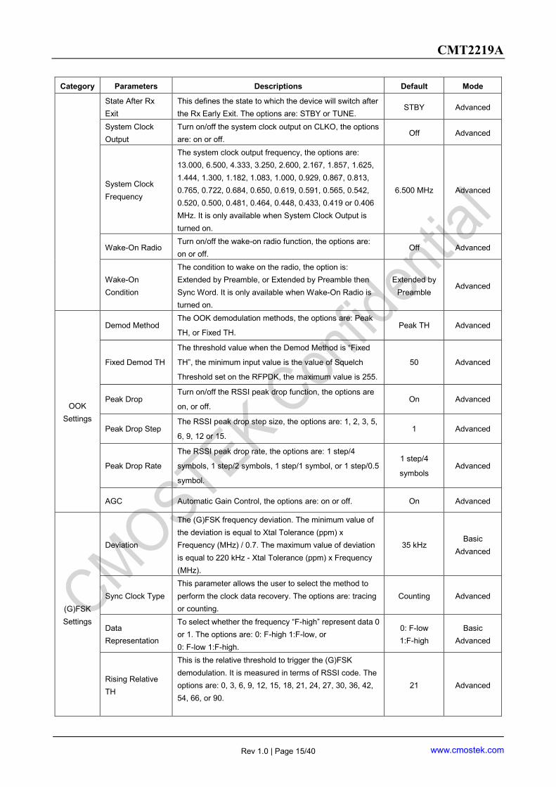
Category Parameters Descriptions Default Mode
State After Rx
Exit
This defines the state to which the device will switch after
the Rx Early Exit. The options are: STBY or TUNE. STBY Advanced
System Clock
Output
Turn on/off the system clock output on CLKO, the options
are: on or off. Off Advanced
System Clock
Frequency
The system clock output frequency, the options are:
13.000, 6.500, 4.333, 3.250, 2.600, 2.167, 1.857, 1.625,
1.444, 1.300, 1.182, 1.083, 1.000, 0.929, 0.867, 0.813,
0.765, 0.722, 0.684, 0.650, 0.619, 0.591, 0.565, 0.542,
0.520, 0.500, 0.481, 0.464, 0.448, 0.433, 0.419 or 0.406
MHz. It is only available when System Clock Output is
turned on.
6.500 MHz Advanced
Wake-On Radio Turn on/off the wake-on radio function, the options are:
on or off. Off Advanced
Wake-On
Condition
The condition to wake on the radio, the option is:
Extended by Preamble, or Extended by Preamble then
Sync Word. It is only available when Wake-On Radio is
turned on.
Extended by
Preamble Advanced
OOK
Settings
Demod Method The OOK demodulation methods, the options are: Peak
TH, or Fixed TH. Peak TH Advanced
Fixed Demod TH
The threshold value when the Demod Method is “Fixed
TH”, the minimum input value is the value of Squelch
Threshold set on the RFPDK, the maximum value is 255.
50 Advanced
Peak Drop Turn on/off the RSSI peak drop function, the options are
on, or off. On Advanced
Peak Drop Step The RSSI peak drop step size, the options are: 1, 2, 3, 5,
6, 9, 12 or 15. 1 Advanced
Peak Drop Rate
The RSSI peak drop rate, the options are: 1 step/4
symbols, 1 step/2 symbols, 1 step/1 symbol, or 1 step/0.5
symbol.
1 step/4
symbols Advanced
AGC Automatic Gain Control, the options are: on or off. On Advanced
(G)FSK
Settings
Deviation
The (G)FSK frequency deviation. The minimum value of
the deviation is equal to Xtal Tolerance (ppm) x
Frequency (MHz) / 0.7. The maximum value of deviation
is equal to 220 kHz - Xtal Tolerance (ppm) x Frequency
(MHz).
35 kHz Basic
Advanced
Sync Clock Type
This parameter allows the user to select the method to
perform the clock data recovery. The options are: tracing
or counting.
Counting Advanced
Data
Representation
To select whether the frequency “F-high” represent data 0
or 1. The options are: 0: F-high 1:F-low, or
0: F-low 1:F-high.
0: F-low
1:F-high
Basic
Advanced
Rising Relative
TH
This is the relative threshold to trigger the (G)FSK
demodulation. It is measured in terms of RSSI code. The
options are: 0, 3, 6, 9, 12, 15, 18, 21, 24, 27, 30, 36, 42,
54, 66, or 90.
21 Advanced

CMT2219A
Rev 1.0 | Page 16/40
www.cmostek.com
Category Parameters Descriptions Default Mode
Falling Relative
TH
This is the relative threshold to shut down the (G)FSK
demodulation. It is measured in terms of RSSI code. The
range is from 0 to 255.
255 Advanced
AFC Turn on/off the Automatic Frequency Control function.
The options are: On or Off. On Advanced
Decode
Settings
Data Mode The data acquisition mode, the options are: Direct, Buffer
or Packet. Packet
Basic
Advanced
Packet Type The device can support two packet types. The options
are: Fixed length or Variable length. Fixed Length
Basic
Advanced
FIFO Threshold
This defines the FIFO threshold that once it is reached,
an interrupt is generated to notify the external MCU. The
range is from 1 to 32, in terms of the FIFO address.
32 Basic
Advanced
De-Whitening
Seed
This parameter is only available when DC-Free Data
Decode is not set to “None”. The initial seed for the data
de-whitening polynomial. The range is from 0 to 255.
NA Basic
Advanced
DC-Free Decode
The options of DC-free data decoding are None,
Manchester 1 (01=one, 10=zero), Manchester 2 (10=
one, 01=zero), or Data De-whitening.
None Basic
Advanced
Preamble The size of the valid preamble, the options are: None,
1-byte, 2-byte, 3-byte, or 4-byte. 2-byte
Basic
Advanced
Sync Size
The size of the Sync Word, the options are: None, 1-byte,
2-byte, 3-byte, or 4-byte. This option cannot be set to
“None” in buffer mode.
3-byte Basic
Advanced
Sync Value
This parameter is only available when Sync Size is not
set to “None”. It defines the value of the Sync Word, the
range is from 0 to 2N-1, where N is determined by Sync
Size. For example, if Sync Size is 1-byte, N is 8; if Sync
Size is 2-byte, N is 16, etc.
0 Basic
Advanced
Sync Tolerance
The number of bits tolerated for the Sync Word
recognition. The options are: None, 1 Error, 2 Errors or 3
Errors.
None Basic
Advanced
Node ID Options
The options for the Node ID detection are: None, Detect
Node ID, Detect Node ID and 0x00, or Detect Node ID,
0x00 and 0xFF
None Basic
Advanced
Node ID Value
This parameter is only available when the Node ID
Options is not set to “None”. It defines the value of the
Node ID. The range is from 0 to 255.
NA Basic
Advanced
Data Length This defines the number of bytes of data in a fixed length
packet. The range is from 0 to 32. 32
Basic
Advanced
CRC Options The options for the CRC are: None, CCITT or IBM. None Basic
Advanced
CRC Seed
This parameter is only available when CRC Options is not
set to “None”. It defines the initial seed for the CRC
polynomial. The range is from 0 to 65535.
NA Basic
Advanced

CMT2219A
Rev 1.0 | Page 17/40
www.cmostek.com
5.5 Internal Blocks Description
5.5.1 RF Front-end and AGC
The CMT2219A features a low-IF receiver. The RF front-end of the receiver consists of a Low Noise Amplifier (LNA), I/Q mixer
and a wide-band power detector. Only a low-cost inductor and a capacitor are required for matching the LNA to any common
used antennas. The input RF signal induced on the antenna is amplified and down-converted to the IF frequency for further
processing.
By means of the wide-band power detector and the attenuation networks built around the LNA, the Automatic Gain Control (AGC)
loop regulates the RF front-end’s gain to get the best system linearity, selectivity and sensitivity performance, even though the
receiver suffers from strong out-of-band interference.
5.5.2 IF Filter
The signals coming from the RF front-end are filtered by the fully integrated 3rd-order band-pass image rejection IF filter which
achieves over 35 dB image rejection ratio typically. The IF center frequency is dynamically adjusted to enable the IF filter to
locate to the right frequency band, thus the receiver sensitivity and out-of-band interference attenuation performance are kept
optimal despite the manufacturing process tolerances. The IF bandwidth is automatically computed according to the three basic
system parameters input from the RFPDK: RF frequency, Xtal tolerance, and symbol rate.
5.5.3 RSSI
The subsequent multistage I/Q Log amplifiers enhance the output signal from IF filter before it is fed for demodulation. Receive
Signal Strength Indicator (RSSI) generators are included in both Log amplifiers which produce DC voltages that are directly
proportional to the input signal level in both of I and Q path. The resulting RSSI is a sum of both these two paths. Extending from
the nominal sensitivity level, the RSSI achieves over 66 dB dynamic range.
The CMT2219A integrates a patented DC-offset cancellation engine. The receiver sensitivity performance benefits a lot from the
novel, fast and accurate DC-offset removal implementation.
5.5.4 SAR ADC
The on-chip 8-bit SAR ADC digitalizes the RSSI output. When receiving a FSK or GFSK modulated signal, the digitized RSSI is
used to turn on and off the (G)FSK demodulator. When receiving an OOK modulated signal, it is used for OOK demodulation in
the digital domain.
5.5.5 Crystal Oscillator
The crystal oscillator is used as the reference clock for the PLL frequency synthesizer and system clock for the digital blocks. A
26 MHz crystal should be used with appropriate loading capacitors (C2 and C3 in Figure 9, Page 11). The values of the loading
capacitors depend on the total load capacitance CL specified for the crystal. The total load capacitance seen between the XIN
and XOUT pin should equal CL for the crystal to oscillate at 26 MHz.
CL =1
1C2
1C3
++ Cparasitic
The parasitic capacitance is constituted by the input capacitance and PCB tray capacitance. The ESR of the crystal should be
within the specification in order to ensure a reliable start-up. An external signal source can easily be used in place of a
conventional XTAL and should be connected to the XIN pin. The incoming clock signal is recommended to have a peak-to-peak
swing in the range of 300 mV to 700 mV and AC-coupled to the XIN pin.
CMT2219A
Rev 1.0 | Page 18/40
www.cmostek.com
5.5.6 Frequency Synthesizer
A fractional-N frequency synthesizer is used to generate the LO frequency for the down conversion I/Q mixer. The frequency
synthesizer is fully integrated except the VCO tank inductor which enables the ultra low-power receiver system design. Using the
26 MHz reference clock provided by the crystal oscillator or the external clock source, it can generate any receive frequency
between 300 to 960 MHz with a frequency resolution of 24.8 Hz.
The VCO always operates at 2x of LO frequency. A high Q (at VCO frequency) tank inductor should be chosen to ensure the
VCO oscillates at any conditions meanwhile burns less power and gets better phase noise performance. In addition, properly
layout the inductor matters a lot of achieving a good phase noise performance and less spurious emission. The recommended
VCO inductors for different LO frequency bands are shown as bellow.
Table 11. VCO Inductor for Common Used Frequency Bands
LO Frequency Band (MHz) 315 433.92 868.35 915
VCO Inductor (nH) 33 18 3.9 3.9
Multiple subsystem calibrations are performed dynamically to ensure the frequency synthesizer operates reliably in any working
conditions.
5.5.7 LPOSC
An internal 1 kHz low power oscillator is integrated in the CMT2219A. It generates a clock to drive the sleep timer to periodically
wake the device up from sleep state. The Sleep Time can be configured from 3 to 134,152,192 ms (more than 37 hours) when
the device works in duty-cycle receive mode. Since the frequency of the LPOSC drifts when the temperature and supply voltage
change, it is automatically calibrated during the PUP state, and is periodically calibrated since then. The calibration scheme
allows the LPOSC to maintain its frequency tolerance to less than ±1%.
5.5.8 OOK Demodulation
The OOK demodulation is done by comparing the RSSI to a demodulation threshold. The threshold is an 8-bit binary value that is
comparable to the 8-bit digitized RSSI. There are two methods of OOK demodulation supported: Fixed TH and Peak TH. The
symbol rate range for the OOK demodulation is from 0.1 to 40 ksps. More details of the OOK demodulation can be found in the
document “AN138 CMT2219A Configuration Guideline”.
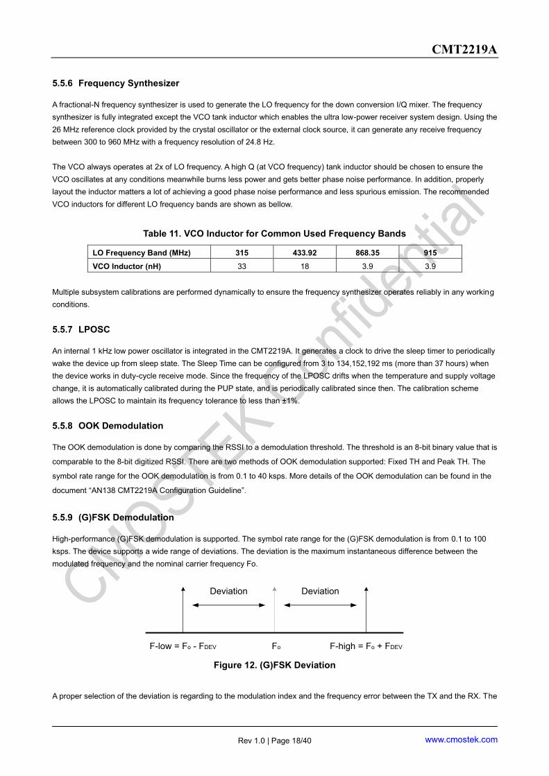
5.5.9 (G)FSK Demodulation
High-performance (G)FSK demodulation is supported. The symbol rate range for the (G)FSK demodulation is from 0.1 to 100
ksps. The device supports a wide range of deviations. The deviation is the maximum instantaneous difference between the
modulated frequency and the nominal carrier frequency Fo.
Deviation Deviation
F-low = Fo - FDEV F-high = Fo + FDEVFo
Figure 12. (G)FSK Deviation
A proper selection of the deviation is regarding to the modulation index and the frequency error between the TX and the RX. The

CMT2219A
Rev 1.0 | Page 19/40
www.cmostek.com
modulation index is given by:
Deviation x 2
Symbol RateModulation Index =
The value of crystal tolerance dominates the frequency error:
Xtal Tolerance x FrequencyFrequency Error >=
By obeying the following rules, the RFPDK automatically computed the minimum value of the deviation that can be configured.
0.7Deviation >=
Symbol Rate x 2Deviation >=
Frequency Error
This means the Modulation Index cannot be less than 1. Also, the deviation must be larger than the frequency error in order to
guarantee the reception. The RFPDK also computes the maximum value of the deviation that can be configured. The following
rule is obeyed:
220 kHz – Frequency Error Deviation <=
Therefore, once the Symbol Rate and Xtal Tolerance are configured on the RFPDK, the configurable range of the Deviation is
automatically obtained.
On the other hand, the FSK demodulation can be automatically turned on and off by detecting the RSSI relative thresholds to
save the power consumption of the device. Automatic Frequency Control (AFC) can be used by the user to minimize/remove the
frequency error between the Tx and the Rx. More details of the (G)FSK demodulation can be found in the document “AN138
CMT2219A Configuration Guideline”.
5.6 SPI Interface
The communication between the MCU and the chip is done via the 4-wire SPI interface. The active-low CSB indicates that the
MCU is trying to access to the registers. The active-low FCSB indicates that the MCU is trying to read the FIFO. The CSB and
FCSB cannot be both set low at the same time. The SCL is the serial clock. For both of the MCU and the chip, data is always sent
at the falling edge of SCL and captured at the rising edge of SCL. The SDA is a bi-directional data pin. Address and data is
always sent starting from the MSB.
5.6.1 Register Read & Write Operation
While accessing to the registers, an r/w bit is sent followed by a 7-bit register address. The MCU must pull the CSB to low at least
half SCL cycle before sending the r/w bit. After issuing the last falling edge of SCL, the MCU must wait for at least half SCL cycle
before pulling the CSB back to high.

CMT2219A
Rev 1.0 | Page 20/40
www.cmostek.com
SCL
CSB
SDA X 01234567 X
register address register read data
01234567
r/w = 1
FCSB
> 0.5 SCL cycle > 0.5 SCL cycle
Figure 13. SPI Read Register Timing
SCL
CSB
SDA X X 01234567 01234567
register address register write data
FCSB
r/w = 0
> 0.5 SCL cycle > 0.5 SCL cycle
Figure 14. SPI Write Register Timing
5.6.2 FIFO Read Operation
When reading the 32-byte FIFO, the internal read pointer will automatically increment after each byte is read out. The MCU must
pull the FCSB to low for at least 1 SCL cycle before issuing the first rising edge of SCL. After issuing the last falling edge of SCL,
the MCU must wait for at least 2 us before pulling the FCSB back to high. Furthermore, the MCU must pull up the FCSB for at
least 4 us before reading the next byte of the FIFO. It allows the internal circuit to generate the FIFO interrupts according to the
current status.
SCL
FCSB
SDA X X
FIFO read data
01234567 01234567X
FIFO read data
CSB
> 1 SCL cycle > 4 us> 2 us > 2 us> 1 SCL cycle
Figure 15. SPI Read FIFO Timing

CMT2219A
Rev 1.0 | Page 21/40
www.cmostek.com
5.7 Operation States, Timing and Power
5.7.1 Power-Up Sequence
The chip operation starts from a valid power-on reset. It usually takes about 0.5 ms for the valid power-on reset to release. Once
the POR is released the crystal oscillator start oscillating. The time taken for the crystal oscillator to get stable is fixed at 2.5 ms in
the first power-up. After the crystal gets stable, it takes about 6.5 ms for the chip to perform the internal blocks calibrations. The
calibrations are only performed once at the beginning of one power-on cycle.
POR
VDD
POR Release
<= 0.5 ms
XTAL Stablize
= 2.5 ms
Blocks Calibrations
<= 6.5 ms
Enters the SLEEP State
Ready to Work
Time
Figure 16. Power-Up Sequence Timing
The chip enters the SLEEP mode as soon as the calibrations are done. From this point on, the MCU can then actively switch the
chip into different operating states by writing the register bits OP_SWITCH<4:0>.
5.7.2 Operating States
There are in all 6 operating states: PUP, SLEEP, STBY, TUNE, RX and EEPROM, as shown in the below table.
Table 12. CMT2219A Operation States
State Command Active Blocks Optional Blocks
PUP soft_reset POR, XTAL None
SLEEP go_sleep SPI, POR LFOSC, Sleep Timer
STBY go_stby SPI, POR, XTAL, FIFO CLKO
TUNE go_tune SPI, POR, XTAL, PLL, FIFO CLKO
RX go_rx All CLKO, RX Timer
EEPROM go_eeprom SPI, POR, XTAL CLKO
The 6 commands used by the MCU to switch the states are simply register-writing operation. Please see OP_CTRL and
SOFTRST register description for the details. The MCU can arbitrarily switch the states, as long as it complies with the switching
time requirement and rules. For example, the MCU can directly switch the chip from SLEEP state to RX state, while it has to wait
for the time of “Xtal Stabilizing Time + 300 us + 20 us” before taking any further actions in the RX state. While switching the states
backward, the time cost is negligible. Switching to the EEPROM state is only allowed in the SLEEP state. The soft reset will pull
the device back to the PUP state and re-perform the blocks calibrations.
CMT2219A
Rev 1.0 | Page 22/40
www.cmostek.com
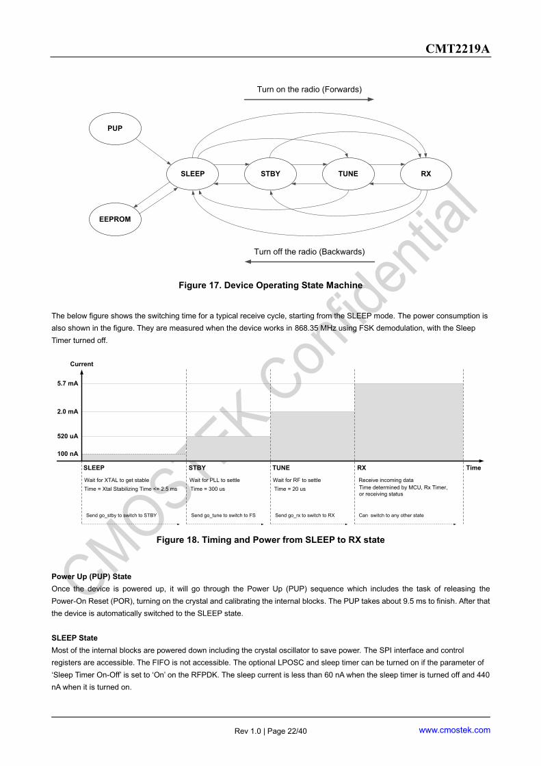
Turn off the radio (Backwards)
PUP
SLEEP STBY TUNE RX
Turn on the radio (Forwards)
EEPROM
Figure 17. Device Operating State Machine
The below figure shows the switching time for a typical receive cycle, starting from the SLEEP mode. The power consumption is
also shown in the figure. They are measured when the device works in 868.35 MHz using FSK demodulation, with the Sleep
Timer turned off.
SLEEP STBY TUNE RX
Send go_stby to switch to STBY Send go_tune to switch to FS Send go_rx to switch to RX
Wait for XTAL to get stable Wait for PLL to settle Wait for RF to settle Receive incoming data
Can switch to any other state
Time = Xtal Stabilizing Time <= 2.5 ms Time = 300 us Time = 20 us Time determined by MCU, Rx Timer,
or receiving status
Time
Current
100 nA
520 uA
2.0 mA
5.7 mA
Figure 18. Timing and Power from SLEEP to RX state
Power Up (PUP) State
Once the device is powered up, it will go through the Power Up (PUP) sequence which includes the task of releasing the
Power-On Reset (POR), turning on the crystal and calibrating the internal blocks. The PUP takes about 9.5 ms to finish. After that
the device is automatically switched to the SLEEP state.
SLEEP State
Most of the internal blocks are powered down including the crystal oscillator to save power. The SPI interface and control
registers are accessible. The FIFO is not accessible. The optional LPOSC and sleep timer can be turned on if the parameter of
‘Sleep Timer On-Off’ is set to ‘On’ on the RFPDK. The sleep current is less than 60 nA when the sleep timer is turned off and 440
nA when it is turned on.

CMT2219A
Rev 1.0 | Page 23/40
www.cmostek.com
STBY State
The crystal oscillator is turned on. The frequency synthesizer and RF front-end are turned off. The FIFO contents retain in the
STBY state. If the sleep timer is turned on, after the sleep timer timeout the chip is automatically switched to the STBY state and
waits for the MCU’s commands. It takes the time defined by the “Xtal Stabilizing Time” on the RFPDK for the device to switch
from the SLEEP state to the STBY state. The power consumption is about 520 uA in the STBY state.
TUNE State
The frequency synthesizer (PLL) is tuned and locked to the desired frequency. The RF front-end is turned off. The FIFO contents
retain in the TUNE state. It takes about 300 us to switch from the STBY state to the TUNE state. The power consumption is about
2 mA in the TUNE state.
RX State
All the blocks are turned on. The chip will receive the incoming signals, output the demodulated data from the GPO pin which is
configured as DOUT or perform the data decoding and buffering with the packet handler and the FIFO. The power consumption
of the RX state depends on the frequency band and the demodulation methods. It only takes about 20 us to switch from the
TUNE state to the RX state.
EEPROM State
This state is designed for the user to get access to the User Space of the EEPROM. The User Space is a 32-byte free space that
allows the users to store their own information. The User Space is independent from the Configuration Space which is used to
store all the parameters downloaded from the RFPDK. The details about how to get access to the User Space can be found in
the” AN136 Accessing the CMT2219A EEPROM”.
5.8 GPOs and Interrupts
Four General Purpose Outputs (GPOs) are available to use.
Table 13. General Purpose Outputs
Pin Name I/O Function
10 GPO1 O Programmable output, options are: nRSTO (default), INT1, INT2 and DOUT
9 GPO2 O Programmable output, options are: INT1 (default), INT2 and DCLK
6 GPO3 O Programmable output, options are: CLKO (default), INT1, INT2 and DOUT
5 GPO4 O Programmable output, options are: DOUT (default), INT1, INT2 and DCLK
The nRSTO and the CLKO are respectively the POR and clock output to drive the external MCU. They are designed to lower the
system application BOM. The DOUT is the demodulated data output and the DCLK is the sync clock output.
The INT1 and INT2 are the two interrupt outputs which response to multiple sources, as listed in table below.
Table 14. Interrupt Sources
Interrupts Descriptions Clearing Methods
RSSI_VLD The RSSI valid interrupt By External MCU
PREAM_VLD The preamble detection interrupt By External MCU
SYNC_PS The sync word detection interrupt By External MCU
NODE_PS The node ID detection interrupt in packet mode By External MCU
CRC_PS The CRC validation successful interrupt in packet mode By External MCU
PKT_DONE The packet receiving done interrupt in packet mode By External MCU
SL_TMO The sleep timer timeout interrupt By External MCU
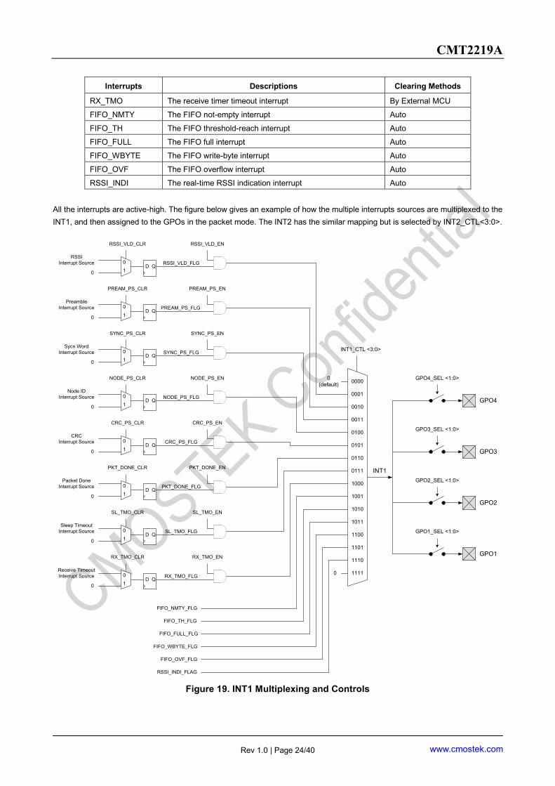
CMT2219A
Rev 1.0 | Page 24/40
www.cmostek.com
Interrupts Descriptions Clearing Methods
RX_TMO The receive timer timeout interrupt By External MCU
FIFO_NMTY The FIFO not-empty interrupt Auto
FIFO_TH The FIFO threshold-reach interrupt Auto
FIFO_FULL The FIFO full interrupt Auto
FIFO_WBYTE The FIFO write-byte interrupt Auto
FIFO_OVF The FIFO overflow interrupt Auto
RSSI_INDI The real-time RSSI indication interrupt Auto
All the interrupts are active-high. The figure below gives an example of how the multiple interrupts sources are multiplexed to the
INT1, and then assigned to the GPOs in the packet mode. The INT2 has the similar mapping but is selected by INT2_CTL<3:0>.
D Q0
10
0000
0001
0010
0011
0100
0101
0110
0111
1000
1001
1010
1011
1100
1101
1110
RSSI_VLD_FLG
RSSI_VLD_CLR RSSI_VLD_EN
D Q0
1
PREAM_PS_FLG
PREAM_PS_CLR PREAM_PS_EN
D Q0
1
SYNC_PS_FLG
SYNC_PS_CLR SYNC_PS_EN
D Q0
1
NODE_PS_FLG
NODE_PS_CLR NODE_PS_EN
D Q0
1
CRC_PS_FLG
CRC_PS_CLR CRC_PS_EN
D Q0
1
PKT_DONE_FLG
PKT_DONE_CLR PKT_DONE_EN
D Q0
1
SL_TMO_FLG
SL_TMO_CLR SL_TMO_EN
D Q0
1
RX_TMO_FLG
RX_TMO_CLR RX_TMO_EN
FIFO_NMTY_FLG
FIFO_TH_FLG
FIFO_FULL_FLG
FIFO_WBYTE_FLG
FIFO_OVF_FLG
RSSI_INDI_FLAG
0
(default)
11110
INT1
GPO4_SEL <1:0>
GPO4
GPO3_SEL <1:0>
GPO3
GPO2_SEL <1:0>
GPO2
GPO1_SEL <1:0>
GPO1
RSSI
Interrupt Source
0
Preamble
Interrupt Source
0
Sycn Word
Interrupt Source
0
Node ID
Interrupt Source
0
CRC
Interrupt Source
0
Packet Done
Interrupt Source
0
Sleep Timeout
Interrupt Source
0
Receive Timeout
Interrupt Source
INT1_CTL <3:0>
Figure 19. INT1 Multiplexing and Controls
CMT2219A
Rev 1.0 | Page 25/40
www.cmostek.com
For those which are cleared by the MCU, each of them has an ‘EN’ bit and a ‘CLR’ register bit. For example, the Sync Word
detection pass interrupt is only enabled when the ‘SYNC_PS_EN’ bit is set to 1, and the interrupt is cleared by setting the
‘SYNC_PS_CLR’ bit to 1. The MCU does not need to set the ‘SYNC_PS_CLR’ bit back to 0 after setting it to 1, because this bit
automatically clears itself once the interrupt is cleared.
The number of available interrupts and their mappings are different in direct mode and buffer mode. For more details of the GPO
controls, please refer to chapter 5.11 User Registers.
5.9 Data Handling
A data path consists of a packet handler and a 32-byte FIFO which is responsible for delivering the data from the demodulator to
the external MCU. It supports 3 data access modes: direct, buffer and packet mode.
5.9.1 Direct Mode
In direct mode, the data from the demodulator’s output is directly sent out to the MCU via the DOUT, which can be mapped to
GPO 1, 3 or 4. The synchronization clock is output via the DCLK, which can be mapped to GPO 2 or 4. The optional preamble
and sync word detection interrupts are supported upon requirements.
DEMODdata
clock
1
1
User Registers
EEPROM (Optional)
RFSPI
CSB
SCL
SDA
DCLK
DOUT
Preamble
(Optional)
Sync
(Optional)data
clock
1
1
INT1/INT2
Figure 20. Data Path of Direct Mode
The data receiving works independently of the preamble and sync word detection in the direct mode. This means, no matter
whether a valid preamble or a sync word is detected or not, the demodulated data will be transparently output on the DOUT.
The sync clock is generated with two purposes: removing the glitches exist on the data output, and assisting the external MCU to
sample the data at the correct instance.
Raw Data
Internal
Sync Clock
Output Data
Output
Sync Clock
1 Symbol
Figure 21. Demodulated Data and Sync Clock Timing Characteristics
CMT2219A
Rev 1.0 | Page 26/40
www.cmostek.com
In the figure above, the raw data is the output of the demodulator. When the SNR of the incoming signal is very low, glitches
possibly exist on the raw data. The device will remove those glitches by internally sampling the raw data using the recovered
clock. The clean data is output to the DOUT. The sync clock is delayed by half cycle and output to the DCLK. The rising edge of
the output sync clock is centered on the output data. If the sync clock is turned off, the raw data will be directly output to the
DOUT.
The sync clock generator produces the clock according to the symbol rate configured on the RFPDK. It can tolerate a certain
amount of symbol rates offset existing between the real incoming signal and the symbol rate input on the RFPDK.. For more
details of the symbol rate offset tolerance, please refers to the “AN138 CMT2219A Configuration Guideline”.
5.9.2 Buffer Mode
In buffer mode, the data from the demodulator’s output are shifted into the 32 x 8-bit parallel FIFO after a valid sync word is
detected. The MCU can use the SPI to read the FIFO. The FIFO will retain its content and be readable in the STBY, TUNE and
RX state. The MCU can use the FIFO interrupts to assist to the FIFO reading. The optional preamble detection is supported.
DEMOD32 x 8-bit
FIFO
User Registers
EEPROM (Optional)
RFSPI
CSB
SCL
SDA
FCSB
INT1
INT2
data
clock
data
8
1
1
Preamble
(Optional)
Sync
(Must)
Figure 22. Data Path of Buffer Mode
Because the chip does all the data buffering work, the MCU can spend time on the other tasks during the buffering process. Also,
it reduces the MCU’s performance requirement in terms of speed and reactivity. The data receiving is independent of the
preamble detection, while the sync word detection is compulsory in the buffer mode.
5.9.3 Packet Mode
In packet mode, the data from the demodulator’s output are first shifted into the packet handler to get decoded, and then filled
into the 32 x 8-bit parallel FIFO.
DEMODPacket
Handler
32 x 8-bit
FIFOdata
clock
data
8
1
1
User Registers
EEPROM (Optional)
RFSPI
CSB
SCL
SDA
FCSB
INT1
INT2
Figure 23. Data Path of Packet Mode
CMT2219A
Rev 1.0 | Page 27/40
www.cmostek.com
Similar to the buffer mode, the data are obtained by reading the FIFO. The packet handler provides various options of decoding
and validating the incoming data. This can further reduce the work load and user program size of the MCU.
Packet Type: Fixed Length
The fixed length means that the payload length is configured into the device and will not be changed during the transmission. The
RX and TX shall have the same payload length in this case. The payload contains the optional Node ID and the Data. The
maximum payload length is limited to the FIFO size which is 32 bytes.
Preamble
Configurable
1 - 4 bytes
Sync
Configurable
1 - 4 bytes
Node ID
Optional
1 byte
Data
Configurable
0 - 31 bytes
CRC
Optional
2 bytes
Optional Manchester or
data-whitening decoding
Payload/FIFO
CRC calculation
Figure 24. Fixed Length Packet Structure
Packet Type: Variable Length
The variable length means that the payload length can vary in different frames. In this case, an additional “Length” byte is given
as the part of the payload to indicate the payload length of the current frame. The maximum payload length can be indicated by
the Length byte is 31, because the Length byte itself is not included in the calculation. For example, if the Length byte indicates
that the payload is 31 bytes, and the Node ID is supported, it means that there will be 1 byte of Node ID and 30 bytes of Data
incoming.
If the Length byte indicates that the payload length is larger than 31, which exceeds the maximum size of the FIFO minus 1, the
current packet will be discarded by the device and the Data will not be shifted into the FIFO.
Preamble
Configurable
1 - 4 bytes
Sync
Configurable
1 - 4 bytes
Node ID
Optional
1 byte
Data
Configurable
0 - 30 bytes
CRC
Optional
2 bytes
Length
1 byte
Payload/FIFO
CRC calculation
Optional Manchester or
data-whitening decoding
Figure 25. Variable Length Packet Structure
For more details of the FIFO and configuring each component of the packet handler, please refer to the “AN138 CMT2219A
Configuration Guideline”.
5.10 Receiver Operation Control
Multiple options, which can be seen in “Table 10 – Operating Setting”, are available for the user to design different operating
behavior of the device. The main purpose of this is to save the power consumption of the system. It can be seen that the device
contains a sleep timer and a receive timer. Also, the device supports the well-known wake-on radio (WOR) operation. Please
refer to the document “AN138 CMT2219A Configuration Guideline” for the details introduction of the operation settings.
CMT2219A
Rev 1.0 | Page 28/40
www.cmostek.com
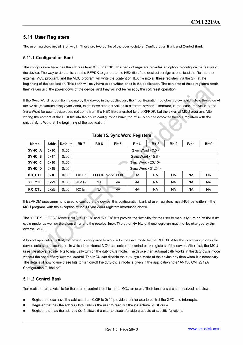
5.11 User Registers
The user registers are all 8-bit width. There are two banks of the user registers: Configuration Bank and Control Bank.
5.11.1 Configuration Bank
The configuration bank has the address from 0x00 to 0x3D. This bank of registers provides an option to configure the feature of
the device. The way to do that is: use the RFPDK to generate the HEX file of the desired configurations, load the file into the
external MCU program, and the MCU program will write the content of HEX file into all these registers via the SPI at the
beginning of the application. This bank will only have to be written once in the application. The contents of these registers retain
their values until the power down of the device, and they will not be reset by the soft reset operation.
If the Sync Word recognition is done by the device in the application, the 4 configuration registers below, which store the value of
the 32-bit (maximum size) Sync Word, might have different values in different devices. Therefore, in that case, the value of the
Sync Word for each device does not come from the HEX file generated by the RFPDK, but the external MCU program. After
writing the content of the HEX file into the entire configuration bank, the MCU is able to overwrite these 4 registers with the
unique Sync Word at the beginning of the application.
Table 15. Sync Word Registers
Name Addr Default Bit 7 Bit 6 Bit 5 Bit 4 Bit 3 Bit 2 Bit 1 Bit 0
SYNC_A 0x16 0x00 Sync Word <7:0>
SYNC_B 0x17 0x00 Sync Word <15:8>
SYNC_C 0x18 0x00 Sync Word <23:16>
SYNC_D 0x19 0x00 Sync Word <31:24>
DC_CTL 0x1F 0x00 DC En LFOSC Mode <1:0> NA NA NA NA NA
SL_CTL 0x23 0x00 SLP En NA NA NA NA NA NA NA
RX_CTL 0x25 0x00 RX En NA NA NA NA NA NA NA
If EEPROM programming is used to configure the device, this configuration bank of user registers must NOT be written in the
MCU program, with the exception of the 4 Sync Word registers introduced above.
The “DC En”, “LFOSC Mode<1:0>”, “SLP En” and “RX En” bits provide the flexibility for the user to manually turn on/off the duty
cycle mode, as well as the sleep timer and the receive timer. The other NA bits of these registers must not be changed by the
external MCU.
A typical application is that, the device is configured to work in the passive mode by the RFPDK. After the power-up process the
device enters the sleep state, in which the external MCU can setup the control bank registers of the device. After that, the MCU
uses the above register bits to manually turn on the duty cycle mode. The device then automatically works in the duty-cycle mode
without the need of any external control. The MCU can disable the duty-cycle mode of the device any time when it is necessary.
The details of how to use these bits to turn on/off the duty-cycle mode is given in the application note “AN138 CMT2219A
Configuration Guideline”.
5.11.2 Control Bank
Ten registers are available for the user to control the chip in the MCU program. Their functions are summarized as below.
Registers those have the address from 0x3F to 0x44 provide the interface to control the GPO and interrupts.
Register that has the address 0x45 allows the user to read out the instantiate RSSI value.
Register that has the address 0x46 allows the user to disable/enable a couple of specific functions.

CMT2219A
Rev 1.0 | Page 29/40
www.cmostek.com
Register that has the address 0x47 allows the user to set and verify the operation modes.
Register that has the address 0x4F is dedicated to the soft reset command.
Table 16. Control Bank Registers
Name Addr Default Bit 7 Bit 6 Bit 5 Bit 4 Bit 3 Bit 2 Bit 1 Bit 0
INT_EN 0x3F 0x00 SL_TMO_EN RX_TMO_EN RSSI_VLD_EN PREM_PS_EN NODE_PS_EN SYNC_PS_EN CRC_PS_EN PKT_DONE_EN
IO_SEL 0x40 0x00 GPO4_SEL<1:0> GPO3_SEL<1:0> GPO2_SEL<1:0> GPO1_SEL<1:0>
INTCTL_A 0x41 0x00 INT2_CTL<3:0> INT1_CTL<3:0>
INTCTL_B 0x42 0x00 SL_TMO_CLR RX_TMO_CLR RSSI_VLD_CLR PREM_PS_EN NODE_PS_CLR SYNC_PS_CLR CRC_PS_CLR PKT_DONE_CLR
INTCTL_C 0x43 0x00 SL_TMO_FLG RX_TMO_FLG RSSI_VLD_FLG PREM_PS_FLG NODE_PS_FLG SYNC_PS_FLG CRC_PS_FLG PKT_DONE_FLG
INTCTL_D 0x44 0x00 RESV FIFO_FULL_FLG FIFO_NMTY_FLG FIFO_TH_FLG FIFO_OVF_FLG FIFO_PKT_CLR RESV RESV
RSSI 0x45 0x00 RSSI_VALUE<7:0>
FUNC_EN 0x46 0x04 RESV SLTIMER_STOP PROD_TEST_EN RESV RESV HS_SPI_EN RESV RESV
OP_CTRL 0x47 0x00 OP_STATUS<2:0> OP_SWITCH<4:0>
SOFTRST 0x4F NA SOFT_RST<7:0>
The detailed descriptions of each register are given below.
Table 17. INT_EN Register
Register Bit RW Bit Name Descriptions
INT_EN
(0x3F)
7 r/w SL_TMO_EN 0: Disable the sleep timer timeout interrupt (default).
1: Enable the sleep timer timeout interrupt.
6 r/w RX_TMO_EN 0: Disable the receive timer timeout interrupt (default).
1: Enable the receive timer timeout interrupt.
5 r/w RSSI_VLD_EN 0: Disable the RSSI valid interrupt (default).
1: Enable the RSSI valid interrupt.
4 r/w PREAM_PS_EN 0: Disable the preamble detection pass interrupt (default).
1: Enable the preamble detection pass interrupt.
3 r/w SYNC_PS_EN 0: Disable the sync word detection pass interrupt (default).
1: Enable the sync word detection pass interrupt.
2 r/w NODE_PS_EN 0: Disable the node ID detection pass interrupt (default).
1: Enable the node ID detection pass interrupt.
1 r/w CRC_PS_EN 0: Disable the CRC validation pass interrupt (default).
1: Enable the CRC validation pass interrupt.
0 r/w PKT_DONE_EN 0: Disable the packet receive finish interrupt (default).
1: Enable the packet receive finish interrupt.
CMT2219A
Rev 1.0 | Page 30/40
www.cmostek.com
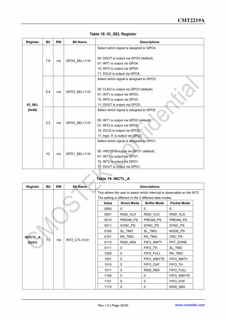
Table 18. IO_SEL Register
Register Bit RW Bit Name Descriptions
IO_SEL
(0x40)
7:6 r/w GPO4_SEL<1:0>
Select which signal is assigned to GPO4.
00: DOUT is output via GPO4 (default).
01: INT1 is output via GPO4.
10: INT2 is output via GPO4.
11: DCLK is output via GPO4.
5:4 r/w GPO3_SEL<1:0>
Select which signal is assigned to GPO3.
00: CLKO is output via GPO3 (default).
01: INT1 is output via GPO3.
10: INT2 is output via GPO3.
11: DOUT is output via GPO3.
3:2 r/w GPO2_SEL<1:0>
Select which signal is assigned to GPO2.
00: INT1 is output via GPO2 (default).
01: INT2 is output via GPO2.
10: DCLK is output via GPO2.
11: logic ‘0’ is output via GPO2.
10: r/w GPO1_SEL<1:0>
Select which signal is assigned to GPO1.
00: nRSTO is output via GPO1 (default).
01: INT1 is output via GPO1.
10: INT2 is output via GPO1.
11: DOUT is output via GPO1.
Table 19. INCTL_A
Register Bit RW Bit Name Descriptions
INTCTL_A
(0x41) 7:4 r/w INT2_CTL<3:0>
This allows the user to select which interrupt is observable on the INT2.
The setting is different in the 3 different data modes.
Value Direct Mode Buffer Mode Packet Mode
0000 0 0 0
0001 RSSI_VLD RSSI_VLD RSSI_VLD
0010 PREAM_PS PREAM_PS PREAM_PS
0011 SYNC_PS SYNC_PS SYNC_PS
0100 SL_TMO SL_TMO NODE_PS
0101 RX_TMO RX_TMO CRC_PS
0110 RSSI_INDI FIFO_NMTY PKT_DONE
0111 0 FIFO_TH SL_TMO
1000 0 FIFO_FULL RX_TMO
1001 0 FIFO_WBYTE FIFO_NMTY
1010 0 FIFO_OVF FIFO_TH
1011 0 RSSI_INDI FIFO_FULL
1100 0 0 FIFO_WBYTE
1101 0 0 FIFO_OVF
1110 0 0 RSSI_INDI

CMT2219A
Rev 1.0 | Page 31/40
www.cmostek.com
The details of each interrupt are introduced in the registers INTCTL_B,
INTCTL_C and INTCTL_D.
The FIFO_WBYTE is the FIFO write-byte strobe that pulses up when
each byte is filled into the FIFO. Because it is a pulse, It cannot be seen
in the INTCTL_C register which reflects the interrupt flags.
3:0 r/w INT1_CTL<3:0> This allows the user to select which interrupt is observable on the INT1.
The interrupt mapping is identical to that of the INT2.
Table 20. INTCTL_B
Register Bit RW Bit Name Descriptions
INTCTL_B[1]
(0x42)
7 w SL_TMO_CLR 0: Keep the sleep timer timeout interrupt (default).
1: Clear the sleep timer timeout interrupt.
6 w RX_TMO_CLR 0: Keep the receive timer timeout interrupt (default).
1: Clear the receive timer timeout interrupt.
5 w RSSI_VLD_CLR 0: Keep the RSSI valid interrupt (default).
1: Clear the RSSI valid interrupt.
4 w PREAM_PS_CLR 0: Keep the preamble detection pass interrupt (default).
1: Clear the preamble detection pass interrupt.
3 w SYNC_PS_CLR 0: Keep the sync word detection pass interrupt (default).
1: Clear the sync word detection pass interrupt.
2 w NODE_PS_CLR 0: Keep the node ID detection pass interrupt (default).
1: Clear the node ID detection pass interrupt.
1 w CRC_PS_CLR 0: Keep the CRC validation pass interrupt (default).
1: Clear the CRC validation pass interrupt.
0 w PKT_DONE_CLR 0: Keep the packet receive finish interrupt (default).
1: Clear the packet receive finish interrupt.
Note:
[1]. Every bit in this register only takes effect in STBY, TUNE, RX and EEPROM state.
Table 21. INTCTL_C
Register Bit RW Bit Name Descriptions
INTCTL_C
(0x43)
7 r SL_TMO_FLG
This interrupt is generated when the sleep timer is turned on and the
SL_TMO_EN is set to 1. The flag goes high at the sleep timer timeout. It
can be cleared by setting the SL_TMO_CLR to 1.
6 r RX_TMO_FLG
This interrupt is generated when the receive timer is turned on and the
RX_TMO_EN is set to 1. The flag goes high at the receive timer timeout.
It can be cleared by setting the RX_TMO_CLR to 1.
5 r RSSI_VLD_FLG
This interrupt is generated when (G)FSK demodulation is used and the
RSSI_VLD_EN is set to 1. The flag goes high when the RSSI exceeds
the FSK Trigger Threshold. It can be cleared by setting the
RSSI_VLD_CLR to 1.
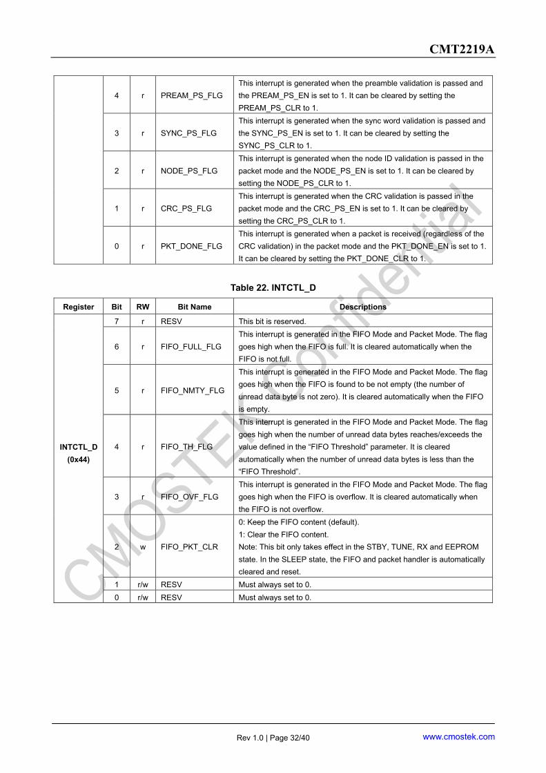
CMT2219A
Rev 1.0 | Page 32/40
www.cmostek.com
4 r PREAM_PS_FLG
This interrupt is generated when the preamble validation is passed and
the PREAM_PS_EN is set to 1. It can be cleared by setting the
PREAM_PS_CLR to 1.
3 r SYNC_PS_FLG
This interrupt is generated when the sync word validation is passed and
the SYNC_PS_EN is set to 1. It can be cleared by setting the
SYNC_PS_CLR to 1.
2 r NODE_PS_FLG
This interrupt is generated when the node ID validation is passed in the
packet mode and the NODE_PS_EN is set to 1. It can be cleared by
setting the NODE_PS_CLR to 1.
1 r CRC_PS_FLG
This interrupt is generated when the CRC validation is passed in the
packet mode and the CRC_PS_EN is set to 1. It can be cleared by
setting the CRC_PS_CLR to 1.
0 r PKT_DONE_FLG
This interrupt is generated when a packet is received (regardless of the
CRC validation) in the packet mode and the PKT_DONE_EN is set to 1.
It can be cleared by setting the PKT_DONE_CLR to 1.
Table 22. INTCTL_D
Register Bit RW Bit Name Descriptions
INTCTL_D
(0x44)
7 r RESV This bit is reserved.
6 r FIFO_FULL_FLG
This interrupt is generated in the FIFO Mode and Packet Mode. The flag
goes high when the FIFO is full. It is cleared automatically when the
FIFO is not full.
5 r FIFO_NMTY_FLG
This interrupt is generated in the FIFO Mode and Packet Mode. The flag
goes high when the FIFO is found to be not empty (the number of
unread data byte is not zero). It is cleared automatically when the FIFO
is empty.
4 r FIFO_TH_FLG
This interrupt is generated in the FIFO Mode and Packet Mode. The flag
goes high when the number of unread data bytes reaches/exceeds the
value defined in the “FIFO Threshold” parameter. It is cleared
automatically when the number of unread data bytes is less than the
“FIFO Threshold”.
3 r FIFO_OVF_FLG
This interrupt is generated in the FIFO Mode and Packet Mode. The flag
goes high when the FIFO is overflow. It is cleared automatically when
the FIFO is not overflow.
2 w FIFO_PKT_CLR
0: Keep the FIFO content (default).
1: Clear the FIFO content.
Note: This bit only takes effect in the STBY, TUNE, RX and EEPROM
state. In the SLEEP state, the FIFO and packet handler is automatically
cleared and reset.
1 r/w RESV Must always set to 0.
0 r/w RESV Must always set to 0.
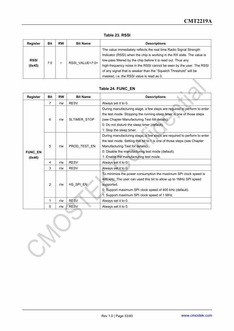
CMT2219A
Rev 1.0 | Page 33/40
www.cmostek.com
Table 23. RSSI
Register Bit RW Bit Name Descriptions
RSSI
(0x45) 7:0 r RSSI_VALUE<7:0>
The value immediately reflects the real time Radio Signal Strength
Indicator (RSSI) when the chip is working in the RX state. The value is
low-pass filtered by the chip before it is read out. Thus any
high-frequency noise in the RSSI cannot be seen by the user. The RSSI
of any signal that is weaker than the “Squelch Threshold” will be
masked, i.e. the RSSI value is read as 0.
Table 24. FUNC_EN
Register Bit RW Bit Name Descriptions
FUNC_EN
(0x46)
7 r/w RESV Always set it to 0.
6 r/w SLTIMER_STOP
During manufacturing stage, a few steps are required to perform to enter
the test mode. Stopping the running sleep timer is one of those steps
(see Chapter Manufacturing Test for details).
0: Do not disturb the sleep timer (default).
1: Stop the sleep timer.
5 r/w PROD_TEST_EN
During manufacturing stage, a few steps are required to perform to enter
the test mode. Setting this bit to 1 is one of those steps (see Chapter
Manufacturing Test for details).
0: Disable the manufacturing test mode (default).
1: Enable the manufacturing test mode.
4 r/w RESV Always set it to 0.
3 r/w RESV Always set it to 0.
2 r/w HS_SPI_EN
To minimize the power consumption the maximum SPI clock speed is
400 kHz. The user can used this bit to allow up to 1MHz SPI speed
supported.
0: Support maximum SPI clock speed of 400 kHz (default).
1: Support maximum SPI clock speed of 1 MHz.
1 r/w RESV Always set it to 0.
0 r/w RESV Always set it to 0.
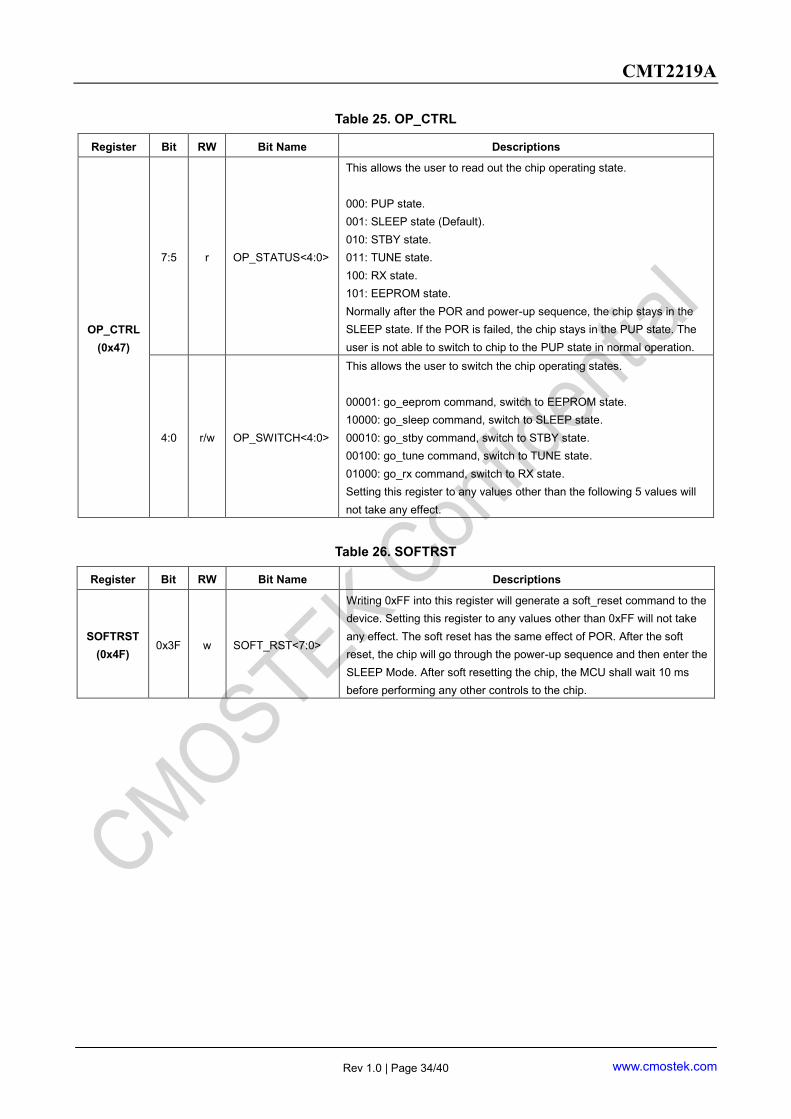
CMT2219A
Rev 1.0 | Page 34/40
www.cmostek.com
Table 25. OP_CTRL
Register Bit RW Bit Name Descriptions
OP_CTRL
(0x47)
7:5 r OP_STATUS<4:0>
This allows the user to read out the chip operating state.
000: PUP state.
001: SLEEP state (Default).
010: STBY state.
011: TUNE state.
100: RX state.
101: EEPROM state.
Normally after the POR and power-up sequence, the chip stays in the
SLEEP state. If the POR is failed, the chip stays in the PUP state. The
user is not able to switch to chip to the PUP state in normal operation.
4:0 r/w OP_SWITCH<4:0>
This allows the user to switch the chip operating states.
00001: go_eeprom command, switch to EEPROM state.
10000: go_sleep command, switch to SLEEP state.
00010: go_stby command, switch to STBY state.
00100: go_tune command, switch to TUNE state.
01000: go_rx command, switch to RX state.
Setting this register to any values other than the following 5 values will
not take any effect.
Table 26. SOFTRST
Register Bit RW Bit Name Descriptions
SOFTRST
(0x4F) 0x3F w SOFT_RST<7:0>
Writing 0xFF into this register will generate a soft_reset command to the
device. Setting this register to any values other than 0xFF will not take
any effect. The soft reset has the same effect of POR. After the soft
reset, the chip will go through the power-up sequence and then enter the
SLEEP Mode. After soft resetting the chip, the MCU shall wait 10 ms
before performing any other controls to the chip.

CMT2219A
Rev 1.0 | Page 35/40
www.cmostek.com
6. Ordering Information
Table 27. CMT2219A Ordering Information
Part Number Descriptions Package
Type
Package
Option
Operating
Condition
MOQ /
Multiple
CMT2219A-EQR[1] 300 – 960 MHz OOK/(G)FSK
receiver QFN16 (3x3) Tape & Reel
1.8 to 3.6 V,
-40 to 85 ℃ 5,000
Note:
[1]. “E” stands for extended industrial product grade, which supports the temperature range from -40 to +85 ℃.
“Q” stands for the package type of QFN16 (3x3).
“R” stands for the tape and reel package option, the minimum order quantity (MOQ) for this option is 5,000 pieces.
The default frequency for CMT2219A is 868.350 MHz, for the other settings, please refer to the Table 10 of Page 14.
Visit www.cmostek.com/products to know more about the product and product line.
Contact [email protected] or your local sales representatives for more information.
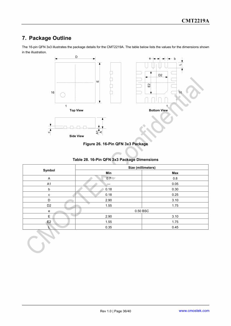
CMT2219A
Rev 1.0 | Page 36/40
www.cmostek.com
7. Package Outline
The 16-pin QFN 3x3 illustrates the package details for the CMT2219A. The table below lists the values for the dimensions shown
in the illustration.
D2
E2
be
L
D
EAA1c
Top View Bottom View
Side View
11
16 16
Figure 26. 16-Pin QFN 3x3 Package
Table 28. 16-Pin QFN 3x3 Package Dimensions
Symbol Size (millimeters)
Min Max
A 0.7 0.8
A1 — 0.05
b 0.18 0.30
c 0.18 0.25
D 2.90 3.10
D2 1.55 1.75
e 0.50 BSC
E 2.90 3.10
E2 1.55 1.75
L 0.35 0.45
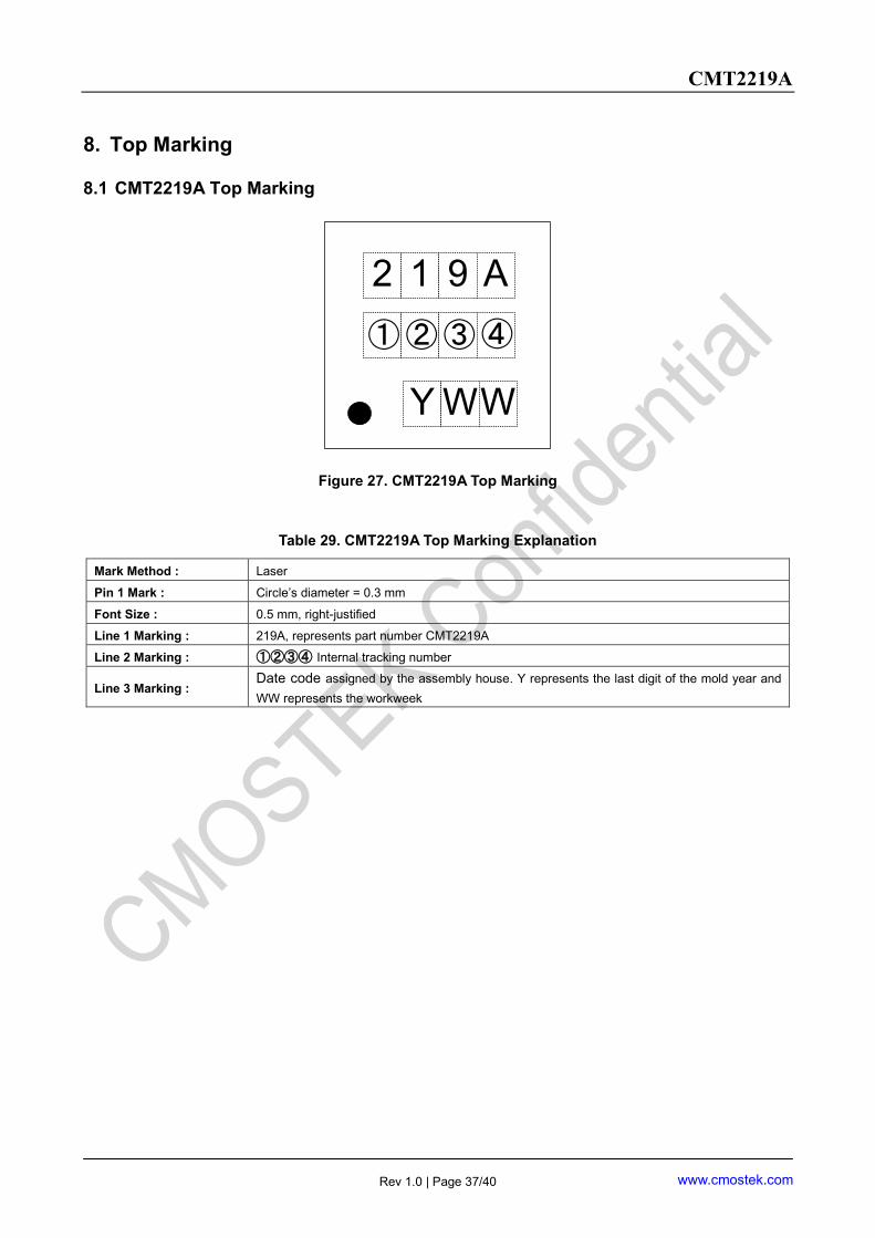
CMT2219A
Rev 1.0 | Page 37/40
www.cmostek.com
8. Top Marking
8.1 CMT2219A Top Marking
2 1 9 A
①②③④
Y WW
Figure 27. CMT2219A Top Marking
Table 29. CMT2219A Top Marking Explanation
Mark Method : Laser
Pin 1 Mark : Circle’s diameter = 0.3 mm
Font Size : 0.5 mm, right-justified
Line 1 Marking : 219A, represents part number CMT2219A
Line 2 Marking : ①②③④ Internal tracking number
Line 3 Marking : Date code assigned by the assembly house. Y represents the last digit of the mold year and
WW represents the workweek

CMT2219A
Rev 1.0 | Page 38/40
www.cmostek.com
9. Other Documentations
Table 30. Other Documentations for CMT2219A
Brief Name Descriptions
AN103 CMT211xA-221xA One-Way RF Link
Development Kits Users Guide
User’s Guides for CMT211xA/221xA Development Kits,
including Evaluation Board and Evaluation Module, CMOSTEK
USB Programmer and RFPDK.
AN136 AN136 Accessing the CMT2219A
EEPROM. Details of how to access the CMT2219A EEPROM.
AN107 CMT221x Schematic and PCB Layout
Design Guideline
Details of CMT221x PCB schematic and layout design rules, RF
matching network and other application layout design related
issues.
AN138 CMT2219A Configuration Guideline Details of configuring CMT2219A features on the RFPDK.
CMT2219A
Rev 1.0 | Page 39/40
www.cmostek.com
10. Document Change List
Table 31. Document Change List
Rev. No. Chapter Description of Changes Date
0.2 All Initial released version 2014-09-10
0.6 5 Update Table 10 2014-09-12
0.7 5.11.2 Correct the typos in Table 19, the higher 4-bit’s Bit Name is
INT2_CTL<3:0> 2014-12-09
0.8 5 Update Table 10, Table 15 and Table 16. 2015-01-23
0.9 0, 4 Update Table 1 and Table8 2015-05-21
1.0 All VCO inductor change 18nH for 433.92MHz 2017-07-11

CMT2219A
Rev 1.0 | Page 40/40
www.cmostek.com
11. Contact Information
CMOSTEK Microelectronics Co., Ltd.
Room 202, Honghai Building, Qianhai Road. Nanshan District
Shenzhen, Guangdong, China PRC
Zip Code:518000
Tel: 0755 - 83235017
Fax: 0755 - 82761326
Sales: [email protected]
Technical support: [email protected]
www.cmostek.com
The information furnished by CMOSTEK is believed to be accurate and reliable. However, no responsibility is assumed for
inaccuracies and specifications within this document are subject to change without notice. The material contained herein is
the exclusive property of CMOSTEK and shall not be distributed, reproduced, or disclosed in whole or in part without prior
written permission of CMOSTEK. CMOSTEK products are not authorized for use as critical components in life support
devices or systems without express written approval of CMOSTEK. The CMOSTEK logo is a registered trademark of
CMOSTEK Microelectronics Co., Ltd. All other names are the property of their respective owners.
Copyright. CMOSTEK Microelectronics Co., Ltd. All rights are reserved.