cny17
DESCRIPTION
CNY17TRANSCRIPT

CNY17 & CNY17F 6-PIN DIP PHOTOTRANSISTOR
OPTOCOUPLER
Product: CNY17 & CNY17F Date: February 1, 2011 Page 1 of 16
Version# 1.1
Feature:
High Isolation voltage between input and output
(Viso = 5000V rms)
Current transfer ratio
CNY17-1, CNY17F-1: 40~80%
CNY17-2, CNY17F-2: 63~125%
CNY17-3, CNY17F-3: 100~200%
CNY17-4, CNY17F-4: 160~320%
Creepage distance > 7.6mm
Operating temperature up to +100°C
The CNY17F Series offers no external base
connection for minimum noise susceptibility
Compact dual-in-line package
Packed in tube or Tape and reel
Conventional black housing package
Schematic:
Certification & Compliance:
Pb free and RoHS Compliant
UL recognized (File # E338132)
VDE recognized (File # 40030457)

CNY17 & CNY17F 6-PIN DIP PHOTOTRANSISTOR
OPTOCOUPLER
Product: CNY17 & CNY17F Date: February 1, 2011 Page 2 of 16
Version# 1.1
Dimension: (Dot location indicates pin 1)
6-Pin Dip (standard):
Wide lead bend (Option W):

CNY17 & CNY17F 6-PIN DIP PHOTOTRANSISTOR
OPTOCOUPLER
Product: CNY17 & CNY17F Date: February 1, 2011 Page 3 of 16
Version# 1.1
SMD lead bend (Option S):
- All Dimensions are in mm
- Tolerance = +/- 0.1mm
CNY17 & CNY17F 6-PIN DIP PHOTOTRANSISTOR
OPTOCOUPLER
Product: CNY17 & CNY17F Date: February 1, 2011 Page 4 of 16
Version# 1.1
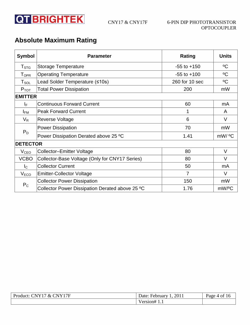
Absolute Maximum Rating
Symbol Parameter Rating Units
TSTG Storage Temperature -55 to +150 ºC
TOPR Operating Temperature -55 to +100 ºC
TSOL Lead Solder Temperature (≤10s) 260 for 10 sec ºC
PTOT Total Power Dissipation 200 mW
EMITTER
IF Continuous Forward Current 60 mA
IFM Peak Forward Current 1 A
VR Reverse Voltage 6 V
PD
Power Dissipation 70 mW
Power Dissipation Derated above 25 ºC 1.41 mW/ ºC
DETECTOR
VCEO Collector–Emitter Voltage 80 V
VCBO Collector-Base Voltage (Only for CNY17 Series) 80 V
IC Collector Current 50 mA
VECO Emitter-Collector Voltage 7 V
PC
Collector Power Dissipation 150 mW
Collector Power Dissipation Derated above 25 ºC 1.76 mW/ºC

CNY17 & CNY17F 6-PIN DIP PHOTOTRANSISTOR
OPTOCOUPLER
Product: CNY17 & CNY17F Date: February 1, 2011 Page 5 of 16
Version# 1.1
Electrical Characteristic (TA=25 oC)
Symbol Characteristic Device Test Condition Range
Unit Min Typ Max
Emitter
VF Forward Voltage CNY17
CNY17F
If = 60mA - - 1.65 V
IR Reverse Current VR = 6V - - 10 µA
Cin Input Capacitance V = 0, f = 1MHz - 18 - pF
Detector Min Typ Max
ICBO Collector-Base Dark Current
CNY17
VCB = 10V, IF= 0 mA
- - 20 nA
BVCBO Collector-Base Breakdown Voltage
IC = 0.1mA, IF= 0 mA
80 - - V
ICEO Collector-Emitter Dark Current
CNY17F
VCE = 10V, IF= 0 mA
- - 50 nA
BVCEO Collector-Emitter Breakdown Voltage
IC = 1mA, IF= 0 mA
80 - - V
BVECO Emitter-Collector Breakdown Voltage
CNY17 CNY17F
IE = 0.1mA, IF= 0 mA
7 - - V
CCE Collector-Emitter Capacitance VCE = 0V, f=1MHz - 8 - pF

CNY17 & CNY17F 6-PIN DIP PHOTOTRANSISTOR
OPTOCOUPLER
Product: CNY17 & CNY17F Date: February 1, 2011 Page 6 of 16
Version# 1.1
DC TRANSFER CHARACTERISTIC
Symbol Characteristic Device Test Condition Range
Unit Min Typ Max
CTR Current Transfer Ratio
CNY17-1 CNY17F-1
VCE = 5V, IF = 10mA
40 - 80
%
CNY17-2 CNY17F-2
63 - 125
CNY17-3 CNY17F-3
100 - 200
CNY17-4 CNY17F-4
160 - 320
CTR Current Transfer Ratio
CNY17-1 CNY17F-1
VCE = 5V, IF = 1mA
13 - -
%
CNY17-2 CNY17F-2
22 - -
CNY17-3 CNY17F-3
34 - -
CNY17-4 CNY17F-4
56 - -
VCE(SAT) Collector-Emitter Saturation Voltage
CNY17 CNY17F
IC = 10mA, IF = 2.5mA
- - 0.3 V
Isolation Characteristic
Symbol Characteristic Device Test Condition Range
Unit Min Typ Max
RIO Isolation Resistance
CNY17 CNY17F
VIO = 500Vdc 1011 - - Ω
CIO Input-output capacitance
VIO = 0, f = 1MHz - 0.5 - pF
Viso Isolation Voltage AC for 1 minute,
R.H. = 40~60%R.H. 5000
V rms
AC Characteristic
Symbol Characteristic Device Test Condition Range
Unit Min Typ Max
Ton Turn-on Time
CNY17 CNY17F
VCC = 10V, IC = 2mA,
RL = 100 Ω
- 10 12
µs
Toff Turn-off Time - 9 12
Tr Rise Time - 6 10
Tf Fall Time - 8 10
Tr Rise Time VCC = 5V, IF = 10mA,
- 2 10
Tf Fall Time - 3 10

CNY17 & CNY17F 6-PIN DIP PHOTOTRANSISTOR
OPTOCOUPLER
Product: CNY17 & CNY17F Date: February 1, 2011 Page 7 of 16
Version# 1.1
RL = 75 Ω
Characteristic Curves:

CNY17 & CNY17F 6-PIN DIP PHOTOTRANSISTOR
OPTOCOUPLER
Product: CNY17 & CNY17F Date: February 1, 2011 Page 8 of 16
Version# 1.1
CNY17 & CNY17F 6-PIN DIP PHOTOTRANSISTOR
OPTOCOUPLER
Product: CNY17 & CNY17F Date: February 1, 2011 Page 9 of 16
Version# 1.1
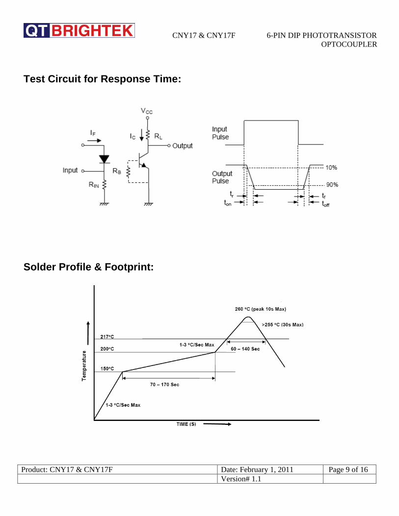
Test Circuit for Response Time:
Solder Profile & Footprint:

CNY17 & CNY17F 6-PIN DIP PHOTOTRANSISTOR
OPTOCOUPLER
Product: CNY17 & CNY17F Date: February 1, 2011 Page 10 of 16
Version# 1.1
Recommended Solder Footprint for SMD Leadform
Units: mm tolerance: +/- 0.1mm

CNY17 & CNY17F 6-PIN DIP PHOTOTRANSISTOR
OPTOCOUPLER
Product: CNY17 & CNY17F Date: February 1, 2011 Page 11 of 16
Version# 1.1
Packing & Labeling: Tape Dimensions:

CNY17 & CNY17F 6-PIN DIP PHOTOTRANSISTOR
OPTOCOUPLER
Product: CNY17 & CNY17F Date: February 1, 2011 Page 12 of 16
Version# 1.1
Device Marking:
Q = QT-Brightek Corporation CNY17(F)-X = Device Part Number (X: 1, 2, 3 or 4) Y = Year WW = Week V = VDE Option

CNY17 & CNY17F 6-PIN DIP PHOTOTRANSISTOR
OPTOCOUPLER
Product: CNY17 & CNY17F Date: February 1, 2011 Page 13 of 16
Version# 1.1
Ordering Information:
Part Number
Orderable Part Number
Options Description Quantity per packing
CNY17-1
CNY17-1 None Standard 6pin DIP 60pcs / Tube
CNY17-1V None Standard 6pin DIP With VDE marking
60pcs / Tube
CNY17-1TA W Wide lead bend (0.4 inch spacing) 60pcs / Tube
CNY17-1TAV W Wide lead bend (0.4 inch spacing) + VDE marking
60pcs / Tube
CNY17-1STA S SMD lead form with tape and reel option
1000pcs / reel
CNY17-1STAV S SMD lead form with tape and reel option + VDE marking
1000pcs / reel
CNY17-2
CNY17-2 None Standard 6pin DIP 60pcs / Tube
CNY17-2V None Standard 6pin DIP With VDE marking
60pcs / Tube
CNY17-2TA W Wide lead bend (0.4 inch spacing) 60pcs / Tube
CNY17-2TAV W Wide lead bend (0.4 inch spacing) + VDE marking
60pcs / Tube
CNY17-2STA S SMD lead form with tape and reel option
1000pcs / reel
CNY17-2STAV S SMD lead form with tape and reel option + VDE marking
1000pcs / reel
CNY17-3
CNY17-3 None Standard 6pin DIP 60pcs / Tube
CNY17-3V None Standard 6pin DIP With VDE marking
60pcs / Tube
CNY17-3TA W Wide lead bend (0.4 inch spacing) 60pcs / Tube
CNY17-3TAV W Wide lead bend (0.4 inch spacing) + VDE marking
60pcs / Tube
CNY17-3STA S SMD lead form with tape and reel option
1000pcs / reel
CNY17-3STAV S SMD lead form with tape and reel option + VDE marking
1000pcs / reel

CNY17 & CNY17F 6-PIN DIP PHOTOTRANSISTOR
OPTOCOUPLER
Product: CNY17 & CNY17F Date: February 1, 2011 Page 14 of 16
Version# 1.1
Part Number
Orderable Part Number
Options Description Quantity per packing
CNY17-4
CNY17-4 None Standard 6pin DIP 60pcs / Tube
CNY17-4V None Standard 6pin DIP With VDE marking
60pcs / Tube
CNY17-4TA W Wide lead bend (0.4 inch spacing) 60pcs / Tube
CNY17-4TAV W Wide lead bend (0.4 inch spacing) + VDE marking
60pcs / Tube
CNY17-4STA S SMD lead form with tape and reel option
1000pcs / reel
CNY17-4STAV S SMD lead form with tape and reel option + VDE marking
1000pcs / reel
CNY17F-1
CNY17F-1 None Standard 6pin DIP 60pcs / Tube
CNY17F-1V None Standard 6pin DIP With VDE marking
60pcs / Tube
CNY17F-1TA W Wide lead bend (0.4 inch spacing) 60pcs / Tube
CNY17F-1TAV W Wide lead bend (0.4 inch spacing) + VDE marking
60pcs / Tube
CNY17F-1STA S SMD lead form with tape and reel option
1000pcs / reel
CNY17F-1STAV S SMD lead form with tape and reel option + VDE marking
1000pcs / reel
CNY17F-2
CNY17F-2 None Standard 6pin DIP 60pcs / Tube
CNY17F-2V None Standard 6pin DIP With VDE marking
60pcs / Tube
CNY17F-2TA W Wide lead bend (0.4 inch spacing) 60pcs / Tube
CNY17F-2TAV W Wide lead bend (0.4 inch spacing) + VDE marking
60pcs / Tube
CNY17F-2STA S SMD lead form with tape and reel option
1000pcs / reel
CNY17F-2STAV S SMD lead form with tape and reel option + VDE marking
1000pcs / reel

CNY17 & CNY17F 6-PIN DIP PHOTOTRANSISTOR
OPTOCOUPLER
Product: CNY17 & CNY17F Date: February 1, 2011 Page 15 of 16
Version# 1.1
Part Number
Orderable Part Number
Options Description Quantity per packing
CNY17F-3
CNY17F-3 None Standard 6pin DIP 60pcs / Tube
CNY17F-3V None Standard 6pin DIP With VDE marking
60pcs / Tube
CNY17F-3TA W Wide lead bend (0.4 inch spacing) 60pcs / Tube
CNY17F-3TAV W Wide lead bend (0.4 inch spacing) + VDE marking
60pcs / Tube
CNY17F-3STA S SMD lead form with tape and reel option
1000pcs / reel
CNY17F-3STAV S SMD lead form with tape and reel option + VDE marking
1000pcs / reel
CNY17F-4
CNY17F-4 None Standard 6pin DIP 60pcs / Tube
CNY17F-4V None Standard 6pin DIP With VDE marking
60pcs / Tube
CNY17F-4TA W Wide lead bend (0.4 inch spacing) 60pcs / Tube
CNY17F-4TAV W Wide lead bend (0.4 inch spacing) + VDE marking
60pcs / Tube
CNY17F-4STA S SMD lead form with tape and reel option
1000pcs / reel
CNY17F-4STAV S SMD lead form with tape and reel option + VDE marking
1000pcs / reel

CNY17 & CNY17F 6-PIN DIP PHOTOTRANSISTOR
OPTOCOUPLER
Product: CNY17 & CNY17F Date: February 1, 2011 Page 16 of 16
Version# 1.1
Revision History:
Description: Revision # Revision Date
Initial of CNY17 & CNY17F Series 1.0 4/27/2010
Feature, certification & compliance and ordering information updates
1.1 02/01/2011
Disclaimer
QT-BRIGHTEK reserves the right to make changes without further notice to any products herein to improve reliability, function or design. QT-BRIGHTEK does not assume any liability arising out of the application or use of any product or circuit described herein; neither does it convey any license under its patent rights, nor the rights of others.
Life Support Policy
QT-BRIGHTEK’s products are not authorized for use as critical components in life support devices or systems without the express written approval of QT-BRIGHTEK. As used herein: 1. Life support devices or systems are devices or systems which, (a) are intended for surgical implant into the body, or (b) support or sustain life, and (c) whose failure to perform when properly used in accordance with instructions for use provided in the labeling, can be reasonably expected to result in a significant injury of the user. 2. A critical component in any component of a life support device or system whose failure to perform can be reasonably expected to cause the failure of the life support device or system, or to affect its safety or effectiveness.