co-emulation of scan-chain based designs utilizing sce-mi
TRANSCRIPT

UNLV Theses, Dissertations, Professional Papers, and Capstones
5-1-2014
Co-Emulation of Scan-Chain Based Designs Utilizing SCE-MI Co-Emulation of Scan-Chain Based Designs Utilizing SCE-MI
Infrastructure Infrastructure
Bill Jason Pidlaoan Tomas University of Nevada, Las Vegas
Follow this and additional works at: https://digitalscholarship.unlv.edu/thesesdissertations
Part of the Computer Engineering Commons, Computer Sciences Commons, and the Electrical and
Computer Engineering Commons
Repository Citation Repository Citation Tomas, Bill Jason Pidlaoan, "Co-Emulation of Scan-Chain Based Designs Utilizing SCE-MI Infrastructure" (2014). UNLV Theses, Dissertations, Professional Papers, and Capstones. 2152. http://dx.doi.org/10.34917/5836171
This Thesis is protected by copyright and/or related rights. It has been brought to you by Digital Scholarship@UNLV with permission from the rights-holder(s). You are free to use this Thesis in any way that is permitted by the copyright and related rights legislation that applies to your use. For other uses you need to obtain permission from the rights-holder(s) directly, unless additional rights are indicated by a Creative Commons license in the record and/or on the work itself. This Thesis has been accepted for inclusion in UNLV Theses, Dissertations, Professional Papers, and Capstones by an authorized administrator of Digital Scholarship@UNLV. For more information, please contact [email protected].

CO-EMULATION OF SCAN-CHAIN BASED DESIGNS UTILIZING SCE-MI
INFRASTRUCTURE
By:
Bill Jason Pidlaoan Tomas
Bachelor‟s Degree of Electrical Engineering
Auburn University 2011
A thesis submitted in partial fulfillment of the requirements for the
Masters of Science in Engineering – Electrical Engineering
Department of Electrical and Computer Engineering
Howard R. Hughes College of Engineering
The Graduate College
University of Nevada, Las Vegas
May 2014
ii
THE GRADUATE COLLEGE
We recommend the thesis prepared under our supervision by
Bill Jason Pidlaoan Tomas
entitled
Co-Emulation of Scan-Chain Based Designed Utilizing SCE-MI
Infrastructure
is approved in partial fulfillment of the requirements for the degree of
Master of Science in Electrical Engineering
Department of Electrical and Computer Engineering
Yingtao Jiang, Ph.D., Committee Chair
Mei Yang, Ph.D., Committee Member
Henry Selvaraj, Ph.D., Committee Member
Evangelos Yfantis, Ph.D., Graduate College Representative
Kathryn Hausbeck Korgan, Ph.D., Interim Dean of the Graduate College
May 2014

iii
Abstract Simulation times of complex System-on-Chips (SoC) have grown exponentially as
designs reach the multi-million ASIC gate range. Verification teams have adopted emulation as a
prominent methodology, incorporating high-level testbenches and FPGA/ASIC hardware for
system-level testing (SLT). In addition to SLT, emulation enables software teams to incorporate
software applications with cycle-accurate hardware early on in the design cycle. The Standard for
Co-Emulation Modeling Interface (SCE-MI) developed by the Accelera Initiative, is a widely
used communication protocol for emulation which has been accepted by major electronic design
automation (EDA) companies.
Scan-chain is a design-for-test (DFT) methodology used for testing digital circuits. To
allow more controllability and observability of the system, design registers are transformed into
scan registers, allowing verification teams to shift in test vectors and observe the behavior of
combinatorial logic. As SoC complexity increases, thousands of registers can be used in a design,
which makes it difficult to implement full-scan testing. More so, as the complexity of the scan
algorithm is dependent on the number of design registers, large SoC scan designs can no longer
be verified in RTL simulation unless portioned into smaller sub-blocks. To complete a full scan
cycle in RTL simulation for large system-level designs, it may take hours, days, or even weeks
depending on the complexity of the circuit.
This thesis proposes a methodology to decrease scan-chain verification time utilizing
SCE-MI protocol and an FPGA-based emulation platform. A high-level (SystemC) testbench and
FPGA synthesizable hardware transactor models are developed for the ISCAS89 S400
benchmark circuit for high-speed communication between the CPU workstation and FPGA
emulator. The emulation results are compared to other verification methodologies, and found to
be 82% faster than regular RTL simulation. In addition, the emulation runs in the MHz speed

iv
range, allowing the incorporation of software applications, drivers, and operating systems, as
opposed to the Hz range in RTL simulation.

v
Acknowledgements The work of this thesis owes the utmost of gratitude to those who contributed to my
academic, professional, and personal growth. Compiled over span of three and a half years, my
thesis has been a collection of industrial experience in the electronic and design automation
(EDA) industry, and a strong foundation of the electrical engineering field set by my professors.
I would like thank my graduate advisor and professor/s, Dr. Yingtao Jiang and Dr. Mei
Yang, for instilling the fundamental theorems, ideas, and principles for verifying digital designs
using field programmable gate arrays (FPGAs). Through a mixture of challenging semester-long
projects and hands-on lab experiments, Dr. Jiang and Dr. Yang ensured my readiness to enter the
industry with experience utilizing the latest tools used by design verification engineers and
system-on-chip designers. Dr. Jiang has also mentored me throughout my entire experience as a
graduate student. He has allowed me to maintain my coursework, providing me flexibility in
balancing the workload between being a student and a verification engineer.
For the duration of my time as a hardware emulation product engineer, I would like to
thank Kryzstof Szcur and Zbigniew Zalewski of Aldec, Inc. Krysztof and Zibi provided me the
opportunity to learn the basics of FPGA-based emulation systems, often begin patient with me
through numerous questions and run-time errors. Together, they both understood that young
engineers brought new ideas to the table when solving existing problems in the emulation
industry. Coupled with guidance in teaching the Standards Co-Emulation Modeling Interface
(SCE-MI), my experience at with Krysztof and Zibi at Aldec allowed me to build on my
verification experience by utilizing the latest in technology and standards.

vi
While studying for my bachelor‟s degree in computer engineering at Auburn University,
I would like to give much appreciation and gratitude to Dr. Charles Stroud. Dr. Stroud provided
me the opportunity to learn more about reconfigurable logic, placing me on his undergraduate
research team working on fault simulation of embedded multiplier built-in-self-test (BIST). With
his extensive background working at Bell Labs, Dr. Stroud taught me everything he knew about
FPGAs, and undoubtedly, is the main reason why I chose digital hardware design and verification
as my main focus in my career.
Lastly, I would like to thank my family and friends for keeping me focused on reaching
my goals, all the while maintaining a sense of humility. The life lessons learned in being both a
student and practicing engineer at times were overwhelming, but thanks to my family and friends,
the weight on my shoulders always seemed manageable.

vii
Table of Contents
Abstract ........................................................................................................................................... iii
Acknowledgements ......................................................................................................................... iv
List of Tables .................................................................................................................................. ix
List of Figures .................................................................................................................................. x
Introduction ...................................................................................................................................... 1
Scan Chain Scalability ................................................................................................................. 2
Scan Insertion .............................................................................................................................. 3
Abstraction Level of Verification ................................................................................................ 5
Event-Based RTL Simulation Bottleneck .................................................................................... 7
HW/SW Development Platforms & Debug ............................................................................... 10
Standard Co-Emulation Modeling Interface (SCE-MI)[19] ............................................................. 16
Usage ......................................................................................................................................... 17
Macro-based message passing interface .................................................................................... 17
Untimed Software Level ........................................................................................................ 18
Cycle-accurate Hardware Level ............................................................................................. 19
Transactions ........................................................................................................................... 20
Controlled and Uncontrolled Time ........................................................................................ 21
Methodology Test Plan .................................................................................................................. 22
Design Under Test – ISCAS S400 Benchmark ......................................................................... 22
Test Bench & Plan ..................................................................................................................... 24
RTL Simulation & Profiling ...................................................................................................... 26
Simulation Acceleration............................................................................................................. 27
Transaction-Based Emulation .................................................................................................... 31
Modified Transaction-Based Emulation ................................................................................ 39
FPGA-based Emulator [22] ...................................................................................................... 41
Results & Analysis ......................................................................................................................... 42
RTL Simulation Results ............................................................................................................. 42
Simulation Acceleration Results ................................................................................................ 46
Transaction-Based Emulation Results ....................................................................................... 49

viii
Pass-Through Transactor ....................................................................................................... 49
FSM Transactor ..................................................................................................................... 54
Complexity Analysis .................................................................................................................. 56
Resource Analysis ...................................................................................................................... 58
Future Work ................................................................................................................................... 61
Conclusion ..................................................................................................................................... 63
Bibliography .................................................................................................................................. 66
CV .................................................................................................................................................. 68

ix
List of Tables
Table 1: Xilinx FPGA Device Properties ........................................................................................ 3
Table 2: Synthesizable vs. Non-Synthesizable Logic .................................................................... 28
Table 3: Test Sequences................................................................................................................. 33
Table 4: RTL Simulation Results .................................................................................................. 45
Table 5: RTL Profiler Results ........................................................................................................ 46
Table 6: Simulation Acceleration Synthesizable Logic ................................................................. 48
Table 7: Synthesizable Logic with Debug Resources .................................................................... 48
Table 8: Simulation Acceleration Results ...................................................................................... 49
Table 9: Estimated vs. Measured Simulation Acceleration Speedup ............................................ 49
Table 10: SCE-MI Pass Through Synthesizable Logic ................................................................. 50
Table 11: SCE-MI Pass Through Synthesizable Logic Debug Resources .................................... 51
Table 12: SCE-MI Pass Through Transactor Results .................................................................... 53
Table 13: Pass Through Transactor Emulation Comparison ......................................................... 54
Table 14: SCE-MI FSM Transactor Synthesizable Logic ............................................................. 55
Table 15: SCE-MI FSM Transactor Synthesizable Logic Debug Resources ................................ 55
Table 16: SCE-MI FSM Transactor Results .................................................................................. 56
Table 17: SCE-MI Emulation Comparisons .................................................................................. 56
Table 18: RTL Simulation Clock Cycle Workload ....................................................................... 57
Table 19: SCE-MI Controlled Clock Cycle Results ...................................................................... 58
x
List of Figures
Figure 1: UVM-based Test Environment......................................................................................... 6
Figure 2: TLM-based Test Environment ......................................................................................... 7
Figure 3: Scan Chain Event-based Simulation ................................................................................ 9
Figure 4: Verification Techniques for Different Levels of Logic .................................................. 10
Figure 5: Aldec FPGA-based Prototyping Platform HES-7 .......................................................... 12
Figure 6: Speed-up vs. HDL Testbench Time ............................................................................... 14
Figure 7: SCE-MI Infrastructure .................................................................................................... 18
Figure 8: Untimed Testbench Models Connected to DUT ............................................................ 19
Figure 9: SCE-MI Abstraction Bridge ........................................................................................... 20
Figure 10: SCE-MI Clocking ......................................................................................................... 22
Figure 11: DFF Scan Conversion .................................................................................................. 23
Figure 12: Top-Level DUT with Scan FFs Instantiated................................................................. 24
Figure 13: Testbench Reset Assertion ........................................................................................... 25
Figure 14: S400 Scan Chain Test Sequence .................................................................................. 26
Figure 15: RTL Simulation Test Environment .............................................................................. 27
Figure 16: Simulation Acceleration Test Enviornment ................................................................. 29
Figure 17: Splitting RTL Simulation Environment for Simulation Acceleration .......................... 30
Figure 18: Emulation Setup Flow .................................................................................................. 31
Figure 19: Testbench Scan Sequence............................................................................................. 34
Figure 20: Transactor Pass Through Assignments ........................................................................ 35
Figure 21: SCE-MI Message In-Port ............................................................................................. 36
Figure 22: SCE-MI Message In-Port Software Implementation .................................................... 37
Figure 23: SCE-MI Pass Through Test Environment .................................................................... 39
Figure 24: SCE-MI FSM Test Environment .................................................................................. 40
Figure 25: Transactor FSM Transitions ......................................................................................... 41
Figure 26: Aldec HES-5 Prototyping Board .................................................................................. 42
Figure 27: TCL Timer Processes ................................................................................................... 44
Figure 28: Simulation Acceleration Emulation Setup ................................................................... 47
Figure 29: SCE-MI Generated XML ............................................................................................. 52
Figure 30: Resource Utilization for Acceleration and Emulation .................................................. 59
Figure 31: LUT Utilization Pre/Post Debug Implementation ........................................................ 61

1
Introduction Integrated circuitry on a grand scale is prevalent in everyday human interaction. These
systems range in complexity from small motor control circuits to large mobile phone system-on-
chips (SoC). As technological processes continue to advance, customers are demanding smaller,
faster, and higher throughput devices. Engineers developing these very large scale integrated
(VLSI) devices, are faced with the challenges of verifying systems which can consists of millions
of gates, mixed-signal (digital and analog) implementations, and new physical characteristics.
To gain controllability and observability into a digital system, designers utilize the „Scan-
Chain‟ testing methodology. This methodology transforms a register to a scan register
(sometimes referred to as a scan flip-flop), by adding a multiplexer circuit at the input of the
register, and a control signal which enables the designer to select between the primary IO and
scan IO [1]. These registers are then serially connected to one another creating a scan chain. With
the scan-chain signals tied to device IO, designers and verification engineers can serially input a
test sequence, and observe the resulting output.
The overall goal of this thesis is to address the issues of scan chain implementation in
large scale SoC devices, and provide a solution which can be quickly integrated into the
traditional digital design and verification flow. In the proceeding section, we observe problems
regarding scan chain scalability when working with multi-million gate system designs. The next
section will cover issues dealing with inserting scan logic into the design at the register transfer
level (RTL). We will also discuss how the abstraction level of digital design verification is being
elevated toward a software-based approach utilizing high-level models. This approach when
coupled with scan chain presents new issues, since hardware developers and software engineers
co-exist on the same platform. Next, the introduction will cover the bottleneck that event-based

2
RTL simulators when simulating scan chain designs. The section will conclude with covering
HW/SW development platforms, in which scan chain designs can be run and debugged.
Scan Chain Scalability
Test methodologies have encountered many issues when dealing with large scale SoC
designs, simply due to the magnitude and complexity of the SoC. Complete systems now
encompass multiple blocks ranging from mixed-signal modules, embedded processors, 3rd
party
intellectual property (IP), and more. Gate count of these systems can quickly grow as all these
modules are put together to form a complete SoC device. Today, an average mobile SoC device is
greater than 4M ASIC gates, and can utilize thousands of registers [2]. For scan chain designs, the
increase in register count is directly dependent on the complexity of the full scan algorithm and
test time [3]. The complexity for full scan method can be calculated as follow:
1. A test vector takes „n‟ clock cycles to be completely shifted in serially to the scan chain
and assert to the combinatorial logic (n+1).
2. The total number of possible combinations for an „n‟ register scan chain is since each
register can exercise a 0 or 1 state.
3. The last test vector takes „n‟ clock cycles to be completely shifted out serially from the
scan chain.
Scan chain implementation transforms a single register to a scan register by
implementing switch logic at the input. This transform causes an additional area penalty to the
circuit, since every register in the design has to undergo the scan transformation. FPGA systems,
platforms commonly used to verify digital designs, are limited by the number of look-up-tables

3
(LUTs) and flip flops available on the device. Although LUT count has steadily increased in
FPGA devices, as shown in table 1 below for Xilinx FPGAs[3] [4] [5] , SoC designs are
advancing at a faster pace than their technological counterpart.
Virtex-5
(XC5VLX330T)
Virtex-6
(XC6VLX760)
Virtex-7
(XC7V2000T)
Slices 51,840 118,560 305,400
LUT Count 207,360 474,240 1,221,600
Max Distributed RAM
(Kb)
3420 8,280 21,550
Table 1: Xilinx FPGA Device Properties
There exist variant scan methodologies, such as partial-scan, in which only a subset of all
registers are transformed into a scan-chain mitigating the area penalty. This variance decreases
the test time and area penalty, but also decreases the effectiveness of the test since all registers
and logic are not tested [7]. For the remainder of this thesis, the scan methodology which will be
used is the full-scan implementation, which utilizes all registers in the design. In addition to full
scan, this thesis will utilize complete test vector set, meaning all possible combinations are
exercised at the scan input. Test compression and automatic test pattern generation (ATPG)
methodologies used to reduce the number of vectors to attain a certain fault coverage (FC%), are
not used in this thesis.
Scan Insertion
Hardware designs typically begin with a user specifications outlining required IO, system
functionality, and expected output. Designer engineers utilize hardware description languages
(HDL) to characterize the system on the RTL level, to be able to observe signal data between
synchronous elements. Verification engineers, often working concurrently with design engineers,
develop testbenches which are used to verify that the circuit is functioning as expected.

4
Testbenches can vary in complexity from simple reset sequences, to comparing packet transfers
between a master and slave device. For scan chain insertion, users have two choices to transform
design RTL code:
1. Manually manipulate the RTL – This includes coding the scan registers at the RTL
level, and adding them to a design hierarchy. This of course it not accomplished on
the system level since it requires scan registers to be added to every block of the
design. The top level only serves to instantiate connections between the modules, or
in this focus, connect scan registers from one block to another The system level
testbench will also require modification, since the system must be tested with the
inserted scan chain. This includes toggling between test data from the user, and
normal system functionality. Manually manipulating the RTL incurs a large time
penalty, since it requires extra coding and verification, but does not require the extra
cost in software test tools.
2. EDA Design-for-Test (DFT) Insertion [8] – EDA vendors tool typically transform
RTL code into a single synthesized netlist. This netlist maps RTL code to gate-level
primitives for ASIC devices, or FPGA primitives for FPGA devices. For the latter,
primitives are stored in FPGA libraries specific for each FPGA vendor. EDA tools
input these FPGA libraries, and transform your design using primitives for the
targeted device. For scan insertion, the user generally specifies test signals to be used
in the design. The DFT-insertion tool generally has its own libraries used for scan
insertion, which modify the primitives used by the FPGA vendor. This way they can
manipulate the netlist by adding scan logic to existing register primitives. Most
software tools also contain scan compression algorithms and built-in fault simulators,
which can generate automatic testbenches for the scan inserted design. Although this

5
allows for faster bring-up of the design, DFT-insertion tools can be quite expensive.
For projects with a restricted budget, extra test software/hardware may not be
feasible.
The difficulty in using scan test for large SoC designs, is balancing the verification of
scan logic and test time. Companies with large design teams have dedicated bandwidth for DFT-
implementation or have access to software tools. Most of the project time is consumed by
verification engineers, since every mode and functionality of the circuit must be exercised in the
testbench [9]. From the previous section, we can see that the complexity of the scan algorithm
exponentially increases as the number of registers in the design increases. Since the testbench
HDL has to be modified to observe data signals from the scan registers, this incurs a longer
verification cycle if a large amount of registers are used.
Abstraction Level of Verification
When designing systems on the block level, hardware designers create testbenches
specific to that blocks functionality. When block level specifications are finished, verification
teams validate the top level, or system functionality. Tests on the system level are more complex
than the block level, since the system usually has to communicate with outside interfaces which
transmit real-time data. For example, when developing a router, the DUT has to interface with a
host workstation via Ethernet to observe packet transfers. To tackle the complexity of validating
at the system-level, verification engineers typically utilize higher levels of abstraction with
hardware verification languages (HVL). HVL‟s such as SystemVerilog, SystemC, C, and C++
contain libraries which contain sequencers, scoreboards, code coverage, and many other tools
which aid in the verification process. Figure 1 showcases a test environment based of the
universal verification methodology (UVM), a verification extension of the SystemVerilog
language [10].

6
Figure 1: UVM-based Test Environment
Since higher levels of abstraction are being used to validate SoC designs, they should
also incorporate test environments aimed specifically for scan design. Classes and functions
utilizing HVLs can be created to automatically handle each step in the scan process. This allows
for different possibilities in handling scan data such as: dumping data to text files, comparing
output vectors against a golden set, and utilizing software constructs for scan automation. This
however poses a challenge since design and verification engineers use different languages in
accomplishing their goals.
Design engineers utilize low-level of abstraction with Verilog and VHDL, while
verification engineers mainly commonly SystemVerilog, SystemC, C, and C++. While there has
been a push for integration between HVLs and HDLs, typically engineering teams use this
structure. For example, SystemC is an event-drive interface between high-level C++ and RTL,
which provide SW engineers an environment to simulate hardware models [11]. These models,
called transaction level modeling (TLM) blocks are written in C++ and can be simulated and
connected to HW RTL models through a programming language interface (PLI). Moreover,

7
software engineers can utilize these high level HW models into an environment to test against
while developing software drivers, applications, and operating systems [12]. Figure 2 showcases
a complete verification environment encompassing TLM models with verification constructs
available in HVLs.
Figure 2: TLM-based Test Environment
For scan based design in today SoC, a verification methodology must be developed
which integrates high level verification, with low level functionality. These two environments and
teams should be separated when establishing scan RTL and verification plans for the scan chain,
but must utilize a standard process which encapsulates both into a single validation cycle. This
will allow the verification team to develop test plans and TLM models with high levels of
abstraction for HW/SW integration, while allowing HW engineers to reuse pre-existing RTL
testbenches.
Event-Based RTL Simulation Bottleneck
The previous sections outlined various issues dealing with algorithm complexity and
RTL issues when adding scan registers to large scale SoC systems. This section will discuss
issues during verification of scan chain systems using RTL simulators. RTL simulation test time
is dictated by the complexity of the test bench and the design, and the workstation CPU. Another
factor is the RTL simulation tool used by the verification team. There are two types of RTL

8
simulators used for verification: event-based and cycle-based. Since the simulator we will be
using (Aldec Riviera-PRO) in this thesis will be event-based, we will focus on its specific
bottleneck.
An event-based simulator updates whenever an event occurs, be it combinatorial or
sequential [13]. Event-based simulators can capture transitions through a combinatorial datapath,
which may not be aligned with a clock edge allowing users to capture issues such as glitches.
Events are placed in a timing queue, which is evaluated in the order the events are placed [14]. In
terms of CPU usage, a majority of the workload is utilized to update the events queue. For a
design with a large number of events, the design queue will be constantly updated, leading to
large simulation times.
For scan chain verification, there exist a large number of events, since data must pass
through both sequential and combinational paths in a single clock cycle. Figure 3 shows cases a
scan chain operation, and how an event-based simulator would fill the timing queue. First is to
assert test mode through all switch logic on the scan registers. Since all events are captured, the
transition from normal mode to test mode is placed in the events queue for all scan registers.
After inputting data the TDI pin, a clock is applied, and the state of each register changes. The
clock transitions and register states changing are all added to the timing queue. After applying the
complete vector into the chain, the test mode is de-asserted, and all switch logic must be
transitioned back to normal mode. As previous, all state changes to the switch logic is then added
to the queue. After a clock cycle is applied, register data must pass through combinational logic in
which the numbers of events added are dependent on logic level/gates. If there is a large amount
of combination logic between registers, than the events queue can grow quickly since there exists
combination paths between all „n‟ number of registers.

9
Scan Chain Operation
Event-based Simulation
Queue
Assert test mode Assert test mode
Input TDI (single bit) Scan register 0 MUX switches to test mode
.
Scan register „n‟ MUX switches to test mode
Apply clock Input TDI (single bit)
Repeat for „N‟ number of registers and clock
cycles until complete vector is shifted-in
Apply clock
De-assert test mode Repeat for „N‟ number of registers and clock
cycles until complete vector is shifted-in
Apply clock De-assert test mode
Output TDO (single bit) Scan register 0 MUX switches to normal mode
.
Scan register „n‟ MUX switches to normal mode
Repeat for possible combinations Apply Clock
Data signal changes through combinatorial path 0
.
.
Data signal changes through combination path n
Output TDO (single bit)
Repeat for possible combinations
Figure 3: Scan Chain Event-based Simulation

10
As seen how above, depending on the number of registers, and the combinatorial path
between those registers, the event queue can grow very large. Since large SoC designs can
contain thousands of registers, simulation time can take hours or even days depending on the
system complexity. Also, a bulk of the transitions occurs between the combinatorial paths
between all scan registers. To speed up this process, we need to utilize a development platform
which will allow us to place the scan chain into hardware and remove it from the simulation
environment.
HW/SW Development Platforms & Debug
In the previous sections, I discussed the challenges in verifying scan based designs such
as: scan insertion, high level of abstraction with HVLs, and increased algorithm complexity when
dealing with a large number of scan registers. This section will address issues and use cases
when utilizing different development platforms for scan testing. Each platform has advantages
and disadvantages in terms of: speed, cost, debug capabilities, and bring-up. Figure 4 showcases
the various platforms with the different HW/SW levels which is applicable for verification [15].
Figure 4: Verification Techniques for Different Levels of Logic

11
For each platform, we will discuss use cases and how scan chain verification can be
accomplished. The four main HW/SW development platforms for SoC designs are:
1. Testbench (RTL) Simulation – This is the main way of verifying design blocks utilizing
Verilog, VHDL, or SystemVerilog. Besides utilizing language specific constructs such as
monitors, random sequence generators, waveform dumps, etc., verification
methodologies such as UVM or OVM have made the verification process more complete.
For scan testing, a user can simply initialize test vectors established from fault simulation
into a text file, and use HDL constructs to feed the data serially into the scan data input.
In similar fashion, data from the scan out can be outputted to a text file to be analyzed at
a later time or compared to against a golden set. The biggest advantage of using RTL
simulation is that all signal transitions are presented to the user through waveform
viewers, schematic editors, and various debug tools available for each EDA vendor. If
there is an incorrect value in the scan out output, user can observe all signals in the chain
as well as the current state all scan registers. This allows the user to quickly debug a
broken scan chain. Although this is the lowest cost of all platforms, we see from the
previous sections that large SoC designs incur very long simulation cycles. In this
manner, a scan chain cannot quickly be verified on the system level because bugs can
only be found at the end of the simulation run.
2. FPGA-based Prototyping – Prototyping platforms, such as the Aldec HES-7 show in
Figure 5 below, utilize FPGA place and route process with a generated bitstream which is
implemented onto FPGA memory [16]. RTL is synthesized and mapped to FPGA
primitives, which then runs through a placer which connects the primitives with FPGA
interconnect. All data being passed through the FPGA place and route (PNR) process
must be synthesizable, meaning the code must be able to be mapped onto FPGA

12
primitives. This does not include typical testbench constructs such: delays, initial values,
or system functions.
Figure 5: Aldec FPGA-based Prototyping Platform HES-7
Most prototyping boards include peripherals and connectors, (PCIe, RS232, USB,) which
the user can map design IO to a target device. Since the entire design is running in
hardware, it is capable of running at faster clock frequency than RTL simulation. The
disadvantage of using an FPGA-based prototype is there is little debug capabilities since
signals cannot be observed using a waveform viewer [16]. On-board logic analyzers such
as Xilinx ChipScope Pro and Altera SignalTap, mitigate the issue, but with a limited
number of bits to be sampled, they do not provide a complete debug environment.
Debugging a scan chain is difficult when implemented onto an FPGA, since users can
only observe the scan in and scan out data. If a scan register contains an incorrect value,
it must propagate through the entire chain before being observed at the output.

13
3. Acceleration/Emulation – Acceleration and emulation platforms combine the debugging
environment from RTL simulation with the speed of an FPGA prototype. In these
systems, a workstation with an RTL simulator directly connects to a FPGA prototype via
high-speed interfaces (Ethernet, PCIe). Emulation teams develop hardware drivers for
the physical interface and a software library to establish communication between the
hardware and software. From this point, users can utilize two different modes of
operation:
a. Simulation Acceleration [16]
– With this mode, synthesizable constructs are
implemented onto the FPGA hardware, while non-synthesizable (Testbench)
constructs remain in the RTL simulator. Simulation acceleration is a signal-based
interface, as data is passed serially through the high speed channel. This mode is
faster than RTL simulation, if the majority of the simulation time is not spent
inside the testbench. If the testbench contains a majority of the simulation time,
than the emulator will spend a most of the time in the communication structure
between the hardware and software. Most simulators have a profiler tool which
allows the user to locate this module requires the largest amount of CPU usage
and simulation time. With this information, the amount of speedup can be
determined prior to running acceleration. In Figure 6 below, a table is show with
the amount of speed up a design can attain depending on the time spend in the
test bench.
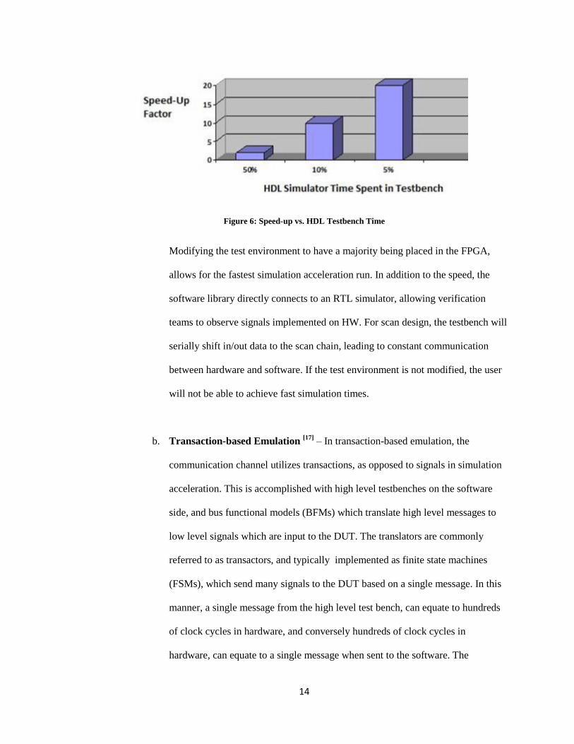
14
Figure 6: Speed-up vs. HDL Testbench Time
Modifying the test environment to have a majority being placed in the FPGA,
allows for the fastest simulation acceleration run. In addition to the speed, the
software library directly connects to an RTL simulator, allowing verification
teams to observe signals implemented on HW. For scan design, the testbench will
serially shift in/out data to the scan chain, leading to constant communication
between hardware and software. If the test environment is not modified, the user
will not be able to achieve fast simulation times.
b. Transaction-based Emulation [17]
– In transaction-based emulation, the
communication channel utilizes transactions, as opposed to signals in simulation
acceleration. This is accomplished with high level testbenches on the software
side, and bus functional models (BFMs) which translate high level messages to
low level signals which are input to the DUT. The translators are commonly
referred to as transactors, and typically implemented as finite state machines
(FSMs), which send many signals to the DUT based on a single message. In this
manner, a single message from the high level test bench, can equate to hundreds
of clock cycles in hardware, and conversely hundreds of clock cycles in
hardware, can equate to a single message when sent to the software. The

15
Accelera Systems Initiative, the creators of SystemC, developed the standard co-
emulation modeling interface (SCEMI), which defines a model for simulations to
run in an emulation environment and vice versa. SCE-MI defines the
communication between transactor/ message port models running in hardware
(clock edges) and high-level testbenches (C/C++ processing). Debug can be
accomplished in the RTL simulator, since the hardware encompasses the
transactor and DUT within the FPGA. Signals sent from the software side
(through the transactor) and the scan chain can be observed on the waveform
viewer, allowing users to debug broken scan chains which have incorrect values.
Since SCE-MI standards define all system clock operations (which includes the
capability to „freeze‟ the clock) – users do have to worry about how clocking and
reset synchronization occurs.
4. Virtual Prototyping [18]
– Virtual platforms allow software engineers to model system-
level behavior using TLM models. These high-level models can be paired with the
development of a software stack, which can model the behavior of a system at real-time
speeds. Today‟s virtual platform systems have a large portfolio of operating systems,
peripherals, processors, bus models, and various blocks which are commonly found in
SoC devices. Software engineers can utilize the TLM models for customer demos which
can present an early reference model prior to hardware development. The disadvantage of
using a virtual prototype is that they are not a good representation of cycle accurate
hardware behavior. In hardware, data signals transition based on clock edges, while TLM
models are processed serially line by line similar to a C/C++ program. Although
SystemC models have improved since being developed in 1999 to model hardware
closely, it cannot be directly translated to FPGA or ASIC gate primitives as easily as
RTL. For scan design, the virtual prototypes utilize high level models, so a high-level

16
model for a serial communication device (ex. JTAG) can be directly connected to the
scan chain. Engineers can utilize C/C++ debugging tools such as the GNU Debugger
(GDB) to observe the software stack while signals transition in and out of the scan chain.
Since these are high-level models, and will not be implemented into an FPGA, they are
only representative of the hardware functionality, and not its implementation behavior.
Depending on which platform is used for hardware and software development, the
debugging capabilities for verifying scan chain implementation differs. The best option
would be to utilize a transaction-based emulation platform, since the scan chain will
implemented on hardware, and can be verified utilizing transactions from high-level
testbenches. Another option available by some FPGA vendors is an FPGA-based emulation
platform, which combines the capabilities of an FPGA-based prototyping board with a
transaction-based emulator. With this test environment, virtual models available from virtual
prototyping solutions can be directly connected to an emulator workstation via software TLM
libraries developed by emulation vendors. With high-level models and verification constructs,
the scan chain can be verified utilizing timing accurate behavior made available by hardware.
Standard Co-Emulation Modeling Interface (SCE-MI)[19]
This thesis will utilize the SCE-MI standard, which was developed by Accelera in 2007
for communication between hardware and software in emulation platforms. It is worth to note a
description of the protocol, to better understand its basic architecture, and use cases when utilized
by verification and design teams. Today, Emulation systems and prototyping platforms have
emerged as popular verification tools when dealing with large scale SoC designs. Unfortunately
engineers have come to many roadblocks when dealing with such tools such as: no debug
capabilities, slow emulation speed, and limited API provided by EDA vendors. The SCE-MI
protocol was developed to solve the many issues presented by verification teams which were
communication bottleneck between hardware and software.

17
Usage
SCE-MI implements a communication infrastructure which allows messages
(transactions) to be passed between high-level software models to the device under test
implemented in hardware. Ports are established on both sides of the hardware and software link,
and messages are conveyed through the link. Since the software side has no notion of a clock,
which is commonly used to control events in hardware, data is processed in a „un-timed‟ fashion.
The SCE-MI architecture is the bridge between the un-timed messages in software and the
„timed‟ clock events occurring in hardware.
Macro-based message passing interface
There are three types of SCE-MI interfaces: macro-based, function-based, and pipes-
based. For this thesis, we will be using function-based and omit the two latter interfaces. There
are 3 main environments when describing the SCE-MI macro-based interface: the hardware side,
the software side, and the SCE-MI bridge. On the hardware side, SCE-MI defines a set of
synthesizable message ports which relay messages to and from the software side. The transactor
is a bus functional model, which translates high level calls from the software side to bit sequences
for the DUT. The SCE-MI Infrastructure (shown in Figure 7 below) also contains dedicated clock
and reset control logic to be able to control system clocks.

18
Figure 7: SCE-MI Infrastructure
The software side on the host workstation contains a set of message port proxies, which
are implemented as C++ objects which allow the SCE-MI API to access the channel. From the
connection to the channel, the proxy can connect to any untimed C model (UTC). The SCE-MI
bridge utilizes a dual –ready handshake, in which software proxies and hardware message ports
use Receive/Transmit ready signals to inform the other side that it is ready to receive or send data.
The bridge channel acts as bi-directional network socket, which carry the message, but it is the
responsibility of the transactor to deliver cycle-accurate information to the DUT.
Untimed Software Level
An untimed environment consists of system level model with a test structure utilizing
C/C++ abstract data types (Figure 8 below). These testbench structures can operate a manner
similar to RTL testbenches, but can incorporate object oriented programming (OOP) features
such as classes, functions, etc. On this level, software engineers can connect the untimed-model
to software applications, drivers, or operating systems to send real-time data to the DUT and
analyze system-level outputs. Eventually the DUT is prepared with RTL models, which describes
the model based on cycle-accurate events. This HDL representation of the DUT will eventually
be compiled and synthesized onto a hardware platform. To save time however, the same test

19
structures which were used in the high-level model can be reused in emulation with low-level
RTL models.
Figure 8: Untimed Testbench Models Connected to DUT
Cycle-accurate Hardware Level
For a cycle-accurate hardware model, the DUT is implemented based on clocked events
which is a more accurate behavior compared to an untimed model on the software side. The SCE-
MI infrastructure enacts message ports on hardware, and defines how transaction can be sent to
those ports from proxies established on the software side. Along with the message input/output
ports are transactors, which translate the high level calls to a sequence of bits which are input
stimuli to the DUT. Conversely output data from the DUT is processed in the transactor, and is
sent to the software side. The SCE-MI standard guarantees delivery of the untimed message
through the transport layer established by the macro-based interface. Figure 9 below, there can
multiple instantiations of transactors connected to multiple blocks with a DUT. For example,

20
multiple high-level testbenches can be testing PCIe, USB, and Ethernet interfaces simultaneously
on a SoC DUT, by instantiating multiple transactor cores and software proxy models.
Figure 9: SCE-MI Abstraction Bridge
Transactions
Transactions beginning on the software side are not constrained to any clocking structure
or event as in hardware. With this capability, they can utilize many OOP techniques such as
functions, classes, or Boolean vectors when sending data to the hardware. This allows passing
messages by value or by reference, but whatever means is chosen, needs to be serialized prior to
traveling over the communication channel. It is the job of the proxy to construct the bit vector,
based on what is sent from the software model. Another job of the proxy is to analyze bit vectors

21
traveling from the hardware to the software side, since it needs to be sent to the software model
(which can be a class, function, etc.).
The hardware side relies on the transactor core to apply stimulus to the DUT based on the
input data delivered from the software side. Based on the data, the transactor applies a sequence
of stimulus which relies on clock edges. Output data from the DUT, is processed from the
transactor core, which is then sent back to the software side for post-processing and debug. The
data which is constructed back to an abstract data type in the software, can span over hundreds of
clock cycles in hardware.
Controlled and Uncontrolled Time
There exist two different clocks in the SCE-MI infrastructure: uncontrolled clock
(Uclock), and controlled clock (Cclock). Uncontrolled clock is the fastest clock available, and is
usually provided by an oscillator on an emulator‟s hardware board. Controlled clock, is the DUT
clock which feeds to all the registers in the system design. Data must be able to traverse the
abstraction bridge from the software side to hardware, without interrupting the current operation
occurring in hardware. When data is sent across the bridge to the message port of a transactor, the
controlled clock „freezes‟ the Cclock and DUT operation, and enables the transactor operation
through the Uclock. Figure 10 displays depicts how frozen cclock would appear on a waveform
viewer. Since the top level of the system is running on Uclock, it can be interfaced with operating
systems, such as Linux, which require a high speed environment to run applications.

22
Figure 10: SCE-MI Clocking
Methodology Test Plan
Design Under Test – ISCAS S400 Benchmark
The DUT which will be used for this thesis is the 1989 International Symposium on
Circuits and Systems (ISCAS89) S400 sequential benchmark circuit. The S400 is a netlist
description of a traffic light controller, which contains 21 registers and 3 primary inputs and 6
primary outputs [20]. The circuit is built with 58 inverters and 106 gates (11 ANDs + 36 NANDs
+ 25 ORs + 34 NORs). The 400 in the circuit description, represents the number of interconnect
lines among the circuit primitives. Amongst the primitives, is a low-level description of a register
module built using inverters, tri-states, and NMOS transistors. To modify the benchmark to
include scan registers, a scan_dff module is defined using an RTL description (Figure 11 below).

23
After the module is defined, all 21 scan registers are daisy-chained to another, with the
first input and last output connected to test data in and test data out respectively. In addition, each
register will have a reset signal to be able to reset the register to a known state prior to the scan
sequence. A „ScanEnable‟ signal is also added to each register to be able to put each register into
test mode or allow normal functionality when de-asserted. Figure 12 below shows the top level of
the DUT with the first 3 scan registers connected to one another. The output of the first scan
register (DFF_0) „TESTL‟ is connected directly to the second scan register (DFF_1) via
ScanDataIn. The original signal is connected to the registers data input, and can be toggled with
the ScanEnable signal. This daisy chain propagates through all 21 scan flip flops, and the output
of DFF_21 is connected to the signal „out_DUT_to_xtor_ScanDataOut_Top‟ which feeds back to
Figure 11: DFF Scan Conversion

24
the transactor. To verify the functionality of the DUT, a testbench will be generated exercising all
possible vector inputs ( and verified using RTL simulation.
Figure 12: Top-Level DUT with Scan FFs Instantiated
Test Bench & Plan
The testbench will verify the functionality of the circuit during RTL simulation. Prior to
creating the testbench, a test plan needs to be created to exercise all modes of operation. Since we
are primarily focusing on scan chain operation, we will need to create multiple test sequences for
the DUT. The four test sequences which will be used are the reset toggle, scan enable toggle, scan
sequence, and clock generation.
The first two test sequence puts the DUT into a known state, and enables operation of the
scan chain. For the reset toggle in Figure 13, an active-high reset signal initializes all scan
registers with a „0‟ value, allowing the DUT to clear any data which may be held during circuit
initialization. During the testbench initialization, the reset is set low and is asserted/de-asserted

25
prior to the scan enable toggle sequence. The scan enable toggle sequence, allows the testbench to
shift in test vectors serially into the test data in port of the first scan register. The scan enable de-
asserts when the vector is completely shifted into the scan-chain, capturing the output of the
combination logical back into the scan chain registers. When the capture is finished, the scan
enable is asserted once more, which shifts out the current vector in the chain while
simultaneously shifting in the next vector in the test sequence.
Figure 13: Testbench Reset Assertion
The scan sequence serially shifts in test vectors in the DUT when the scan enable toggle
sequence is occurring. For the scan sequence, we will exercise full-scan mode, which utilizes all
test vectors from all zeroes to all ones (Figure 14). Since the reset toggle sequence sets the
registers to all zeroes, we can eliminate the first bit vector, and observe the output of combination
logic without the first shift sequence. The next vector (21‟d1) is initialized with a counter, which
increments after the last vector is completely shifted into the scan chain. The counter is
constrained to vectors, and when it reaches the upper-bound, the testbench automatically

26
exits following the last vector being shifted out. The clock generation, generates the clock pulse,
which feeds the scan registers and controls the speed of the DUT. For this simulation we will set
the clock speed to 100MHz with a force command in the simulators debug properties. The main
focus during RTL simulation is to determine where the testbench is spending a majority of the
simulation time in the testbench. Although the clock speed can be adjusted, the CPU will throttle
the performance based on current processes occurring, CPU multi-thread capabilities, CPU cores
available, etc. Using the simulators profiler tool, we can gather a better understanding of how the
CPU handles different portions of the testbench [16].
Figure 14: S400 Scan Chain Test Sequence
RTL Simulation & Profiling
The modified ISCAS S400 netlist will be first simulated with the Aldec Riviera-PRO
functional verification platform [21]. Test bench and test sequence will reside in the workstation
CPU. RTL simulation serves as the median to verify circuit operation, and allow debugging using
the waveform viewer tool. Another feature of Riviera-PRO is the schematic view of the system
(Figure 15), which allows users to visualize data transfers between instances in the DUT. The
testbench based on the test sequence in the prior section (full-scan) is implemented on a HP

27
Laptop with an Intel Core Duo CPU clocked at 2.13 GHz. Scripts are generated for the simulator
to be able to run in batch mode, allowing the CPU to run with less resources than running the
simulator with a graphical user interface (GUI). To be able to benchmark the simulation run-time,
Tcl scripts are created with processes which evaluate system time at the beginning and end of the
simulation.
Figure 15: RTL Simulation Test Environment
Two types of HDL simulation will be run: one run without profiler disabled and one with
profiler enabled. The disabled profiler run, allows us to verify functionality and ensure the circuit
is operating correctly, but does not allow us see the communication bottleneck between the DUT
and the testbench. Since there are possible vectors to be fed as primary inputs, profiler
information is needed to assess the possible speedup that can be attained in simulation
acceleration.
Simulation Acceleration
To reduce the number of events occurring in the CPU, the DUT will be transferred to the
FPGA hardware, and will connect physically to the workstation via PCIe connector. The PCIe
connector will facilitate information serially between the hardware and simulator via a co-
simulation interface. With this methodology, there are two portions of the HDL code:
synthesizable and non-synthesizable.

28
Synthesizable (Implemented on FPGA) Non-Synthesizable (Remains in HDL
Simulator)
Ports Delay statements
Signals and variables Device initialization
Procedures Assign statements
Modules User defined primitives
Functions Force and release
Tasks Time constructs
Table 2: Synthesizable vs. Non-Synthesizable Logic
The DUT portion of the system (ISCAS S400) is a Verilog gate-level netlist, with a scan
flip flop module inserted. Since the DUT is fully synthesizable, it is able to me mapped to FPGA
LUTs and implemented onto hardware. The testbench however contains numerous non-
synthesizable constructs which aid in the debugging process in addition to the waveform and
schematic view. Such tasks include system functions ($display, $strobe, $finish, etc.) which allow
output from the design to the simulator console, which can be dumped to a text file for offline
debug. Scan chain vectors are fed in through dedicated test pins from external sources, so the test
environment must simulate this correctly. The external source in this case will be the HDL
simulator, which will serially input the vectors into each scan register in the DUT implemented
onto the FPGA board (Figure 16). The resultant vector will feed out back to the testbench which
will be outputted onto the console and waveform viewer.

29
Figure 16: Simulation Acceleration Test Enviornment
Figure 17 below displays the separation between the system components which are non-
synthesizable and synthesizable. The emulation compiler, Aldec Hardware Emulation Solutions
Design Verification Manager [22], automatically analyzed RTL sources, and distinguishes
between code which will remain in the simulator, and code which will be implemented onto HW.
The DUT is fully synthesizable and implemented to FPGA LUTs, while the testbench constructs
remain in the HDL simulator. For this design, the non-synthesizable constructs include: Clock
generation, Reset sequence, Scan Sequence, and Scan Enable Sequence. The sequences are
described more in detail in the previous section describing the testbench. The communication
between the HDL simulator and DUT are signal-based, meaning a single bit is transferred over a
single-ended (SE) IO line available on the FPGA. The design has 7 inputs and 7 outputs,
requiring a total of 14 SE IO, but the speed of the simulation is dictated by the transferring of data

30
on these lines.
Figure 17: Splitting RTL Simulation Environment for Simulation Acceleration
The advantage of using simulation acceleration is that the pre-existing testbench from
RTL simulation can be reused. This is beneficial to SoC design teams which are separated into
design and verification units, as there requires no modification to port the design to an
acceleration system. Since the testbench containing all test sequences are already defined [16],
they are ported directly into the emulator for analysis. The complete process for simulation
acceleration is shown in Figure 13 below [23]. The design import stage of acceleration allows
importing the FPGA design libraries or simulation libraries which were used during RTL
simulation. Each file in the library in analyzed by the emulator, and automatically determines the
synthesizable and non-synthesizable code. After the code is analyzed, the user selects a top-level
instance, and configures the emulation options in the second stage. A user can instrument debug
probes, partition design instances in multiple FPGAs, and synthesize the DUT with selected
options with FPGA vendor tools. After running a place-and-route process, which physically maps
the design to FPGA primitives, scripts are automatically generated which instantiate the
communication between the hardware and simulator.

31
Figure 18: Emulation Setup Flow
Transaction-Based Emulation
To utilize transaction-based emulation, there needs to be modification to the done on the
hardware and software side. The pre-existing testbench cannot be used, since the interface SCE-
MI interface uses transactions for communication, as opposed to signals in simulation
acceleration.
Software Side Modifications
1. SystemC Testbench – The biggest change of the test environment will be converting the
testbench sequences to high-level SystemC constructs. Whereas the RTL testbench relied
on events such as the rising edge of a clock, the SystemC testbench focus more towards
the implementation of the sequence, rather than its trigger events. This will be done
through two primary functions: timulus and read. The purpose of the stimulus function is
to generate all test sequences defined from the RTL testbench. Using C/C++ constructs
they are converted to high-level implementation. The sequences are converted as follows:
a. Clock Generation – The clock sequence no longer needs to be implemented in
the testbench since the SCE-MI standard defines clock operations with the
uncontrolled clock and controlled clock. Since the clock itself is required for
hardware operation, two clock related ports must be defined to operate correctly:

32
clock port and clock control. These two ports are directly synthesized onto the
FPGA, and have parameters which can be modified for multiple clocks,
positive/negative edge triggers, duty cycle, and phase.
b. Reset Toggle – Similar to clock generation, SCE-MI defines the reset sequence
of the system with and uncontrolled and controlled reset parameter. The reset
signals are defined in the clock control and clock port, which are directly
synthesized onto the FPGA. User can modify HDL parameters to define the
length of the reset sequence.
c. Scan Enable Toggle – The scan enable toggle sequence is accomplished by
generating a 7-bit vector (similar implementation to RTL
simulation/acceleration), and setting the scan enable input high. For the TDI
value, a value of 0x1 is shifted in after the reset. The data in the scan chain is
shifted out, and verified when received by the results function in the testbench.
After the reset sequence, all scan registers should have a value 0x0, and by
shifting a value of 0x1 into chain, it verifies all registers can change states
correctly. The stimulus function outputs are shown in following table:

33
Test Sequence Stimulus Function Results Function
Clock Generation N/A
(SCE-MI defines system clocks)
N/A
(SCE-MI defines system
clocks)
Reset Toggle N/A
(SCE-MI defines Reset )
N/A
(SCE-MI defines Reset )
Scan Enable Toggle
-Scan Enable = 0 1
-Test Mode = 0 1
-Primary IO = X
-Send testbit „1‟
-Scan Enable= 1 0
Read output vector from
message proxy, and display to
output string construct. Verify
bit vector is of value „1‟.
Scan Sequence
-Scan Enable = 0 1
-Test Mode = 0 1
-Primary IO = X
-input all bit of first test vector
serially to TDI pin with FOR loop
-Scan Enable = 1 0
-Increment test vector
-Loop last 3 steps for all vector
Read output vector from
message proxy, and display to
output string construct
Table 3: Test Sequences
d. Scan Sequence – After the scan enable sequence, the shift register has been
verified to switch reach the 0 state (reset sequence) and 1 state (scan enable
sequence). For this SystemC testbench, there is a 7-bit message which will be
sent to the hardware side. One of the inputs is a dedicated scan in port, which a

34
21-bit test vector will be serially shifted in. In Figure 19 on the left below, shows
the shift and write sequence controlled by a FOR loop construct. The data is first
shifted into hardware, and written to the message port. In the next section, a FSM
is added to decrease the number of write tasks to the hardware. After the FOR
loop has finished for all 21 bits, the data is checked if all combinations have
been exercised, and if not, the testbench deasserts the scan enable, and
increments the test vector (shown in Figure 19 on the right).
Figure 19: Testbench Scan Sequence
2. SCE-MI Software Infrastructure Implementation –The software implementation of
the SCE-MI infrastructure includes the message ports, service handlers, error detection,
and other SCE-MI functionality. The Aldec HES-DVM emulator contains all necessary
C/C++ files for implementing the SCE-MI software infrastructure [22]. The main focus
of the end user (verification team/design team), is to create the high-level testbench and
the transactor with hardware implementation. For this portion, the software SCE-MI
implementation has been tested and verified to operate correctly.
Hardware Side Modifications
1. Transactor development
a. Transactor core – The transactor core receives the transactions from the software
side (inMessage) and sends them to the DUT as signals. For this implementation,

35
the SystemC testbench controls the shift sequence with a FOR loop, so data from
the transactor core is passed connected directly to the DUT. This is sometimes
referred to as a „dummy‟ transactor (shown in Figure 20), since there is no
manipulation of data in the transactor core. In the next section, I will describe a
FSM implementation in HW, which will decrease communication for bit shifts
into the DUT.
Figure 20: Transactor Pass Through Assignments
b. SCE-MI Message Ports – The message port consists of an inPort and outPort.
The outPort sends data from the transactor to the software side, and the inPort
receives data from the software side to the transactor core. The message ports
utilize a dual ready handshake protocol with three primary I/O‟s: ReceiveReady,
TransmitReady, and message as shown in Figure 21 below.

36
Figure 21: SCE-MI Message In-Port
When both the ReceiveReady and TransmitReady are asserted high, the message
is sent to the destination across the channel. This occurs on the active edge of the
Uclock, which allows the ports to be written and read to while DUT is still in
operation. On the software side, when a message port is instantiated (whether it
be in or out) in the testbench, a first-in first-out memory is created where
instructions are stored prior to entering and leaving the proxy. The instruction
from the testbench is sent to the FIFO, where the proxy will wait for the
ReceiveReady on the hardware side. The proxy will assert a TransmitReady (for
an inPort) or ReceiveReady (for an outPort) when the FIFO contains data, and
flush the data out, when ready on the hardware side. Figure 22 below is the C++
implementation of the SCE-MI InPort developed by Aldec which is used in the
SystemC TB.

37
Figure 22: SCE-MI Message In-Port Software Implementation
c. SCE-MI Clock Port – The SCE-MI clock port provides the DUT with a
controlled reset and clock. Through a set of parameters such as clock duty, clock
ratio, phase, and reset cycles, the user can customize how timing and reset is
handled in the circuit. For circuits with multiple clock frequencies, multiple clock
ports have to be instantiated with parameters customized for each clock
frequency. Since the system used in this thesis contains only a single global
clock, one clock port and clock control is needed. If no parameters for the
clocking are set, SCE-MI automatically generates a 1/1 ratio clock, a single clock
with the highest frequency in the system. Most of the time, SCE-MI will grab this
clock from oscillators available on the emulation board. Each EDA vendor
provides the input clock for SCE-MI based on tests and delay analysis on a
specific FPGA board. The end-user need not focus on the clock implementation
in the HW, but only create the necessary clock port, which will call the correct
frequency built on the emulation API.
d. SCE-MI Clock Control – The SCE-MI clock control macro is a macro which
aligns clock edges from the uncontrolled clock and controlled clock. This clock
control enables freezing the DUT controlled clock, while still operating the

38
transactor to receive incoming data from the software side. The main advantage
of this control module, which will be used in the modified core implementation,
is the ability to perform operations on data while the DUT is still „frozen‟.
ReadyForCclock is a signal in the control module that allows the DUT clock to
advance. If data received from the software of the DUT needs to be analyzed,
ReadyForCclock can be set low, which allows operation on the data from the
DUT or software side to occur without the DUT clock running.
To implement the transaction-based approach, there needs to be multiple changes in
the hardware and software environment. This can be difficult, if verification teams
are not accustomed to emulation environment. Standards such as SCE-MI continue to
evolve, as verification teams adopt the standard to speed up verification for multi-
million gate SoC. With all the changes to the test environment, the block level of the
system is shown in Figure 23 below. Two proxies will be instantiated on the software
side, which will be to pass transactions to and from the HW. A C++ function called
„Stimulus‟, will generate all the necessary signals, and generate the test vector which
will be serially shifted into the inPort on the hardware side. The serial shifting is
occurring in the software and is sent bit by bit to the inPort. This method will show
that even though the transactor core and testbench is not optimized, it still incurs a
speedup due to the high-level testbench and hardware implementation. The inPort
will pass through a dummy transactor on the active edge of Uclock (which pauses the
Cclock operating the DUT), and be sent directly to the IO of the DUT. The transactor
will then activate Cclock, allowing the DUT data to propagate to the output signals.
The output data is passed to the outPort, where it is serialized into a single bit vector,
and sent to a Read function which analyzed the data and displays on the user console.
The data can be stored in an output text file for later future analysis.

39
Figure 23: SCE-MI Pass Through Test Environment
Modified Transaction-Based Emulation
For the next implementation, we will modify the previous approach by adding data
manipulation inside the transactor core. Previously a 21-bit vector was generated in the software
and serially shifted via a FOR loop to the dummy transactor core, which passed it directly to the
DUT. For the modified implementation, the test vector will be generated in the software, but the
entire vector will be within the message sent to the transactor core. This cuts out the serial
processing of each bit to the inPort, and the number of writes/reads between the HW/SW
interfaces. The message vector and signals will pass through the transactor core, which contains a
FSM (Figure 24 below) that will serially shift data in to the DUT.

40
Figure 24: SCE-MI FSM Test Environment
The FSM machine (Figure 25), which is regulated by Uclock, will contain multiple state
for all inPort/outPort calls, vector reads, and shifting. As the FSM cycles through all the states,
the scan control signals also regulate the flow of data to the scan chain, as opposed to being in the
testbench in the previous implementation. The inPort/outPort calls regulate the dual ready
handshake protocol, which asserts appropriate signals before and after the shift sequence. After
the shift sequence has finished, the output port transmits data, while new data is called to the
inPort simultaneously. After new data is received the shift sequence begins again. The FSM must
be reset appropriately, so all signals are initialized. The Ureset initializes all signals prior to the
data exchange sequence between the hardware and software. This ensures that the FSM does not
begin in an unknown state.

41
Figure 25: Transactor FSM Transitions
FPGA-based Emulator [22]
The FPGA-based prototype solution which will be used for this thesis is the Aldec
HES5XLX660EX (Figure 26 below), which utilizes two Xilinx XC5VLX330T FPGAs for a total
capacity of 5 million ASIC gates. Users are able to connect the HES5 board to a host workstation
via PCI Express x8 lane communication. A dedicated FPGA provides host interface logic when
connecting the Aldec HES-DVM emulator with the FPGA prototyping board. On the board are
two SO-DIMM sockets, which users can utilize up to 2GB of DDR2 memory for memory
expansion. Also available are external clock inputs, on-board oscillators, and PLL circuitry for
users to implement different clocking schemes in their SoC designs. Users can utilize
daughterboard SAMTEC connectors, each with 124 LVDS to connect external targets to the
FPGA prototyping board. Since the DUT is fairly small, no partitioning will be needed which
enables faster speed. If partitioning was required (large number of IO or large design capacity),
the HES-5 provides 428 SE/ 219 LVDS IO for inter-FPGA communication. The data would need

42
some serial/de-serialization methodology which would enable multiple signals to be processes
over a single IO or LVDS pair.
Figure 26: Aldec HES-5 Prototyping Board
Results & Analysis
RTL Simulation Results
A Verilog testbench is generated for the S400 DUT, with processes executing each of the
test sequences. The testbench is roughly ~150 lines of code, and includes the instantiation of the
DUT module. Inside the testbench is a 21-bit count register, which increments after a test
sequence is fully shifted into the scan chain. After the initial reset sequence, the count value is
serially shifted into the test data input from least significant bit (LSB) to most significant bit.
When the test vector is shifted in, a flag to stop the shift is asserted, and the capture process
begins. The data in the scan chain passes through the gate-level logic, and is captured back into
the scan registers. The data is then shifted out with the same Verilog process that shifts in the
data. For all Verilog files, a timescale of 10ns period is used which equates to a 100MHz clock

43
frequency. The scan out vector is saved in a text file, and when beginning a new shift cycle,
moves to a new line in the text file.
Using Aldec Riviera-PRO functional verification tool, compilation and simulation
macros/scripts are created to automate the simulation process. The simulation process will be
done through batch mode, which utilizes a command line interface as opposed to a graphical user
interface, which requires a larger amount of CPU resources. To calculate the runtime of the
simulation, a TCL script (Figure 27) captures the time of the CPU before and after the simulation
run, and determines the difference between the two times. The time difference is then saved to
text file, which can be observed after the simulation has finished. Riviera-PRO has a TCL based
console, which allows the timer script to be integrated into the macro which runs the compilation
and simulation. The timer process begins once the design is compiled and elaborated. The
elaboration time, is the time required by the simulator to process the RTL source files, and
establish the events queue. This time will not be include in the final run-time calculation, since it
is EDA vendor dependent, and can differ depending on how the simulator processes the RTL
code. After running through Riviera-PRO, the benchmark time for RTL simulation was 921
seconds. The sequence ends with the Verilog $finish command after the last test vector is scanned
out and saved to the text file. The test vectors will be later used as a baseline, or golden reference,
when the test environment is ported to simulation acceleration and emulation.

44
Figure 27: TCL Timer Processes
The next step is a simulation run with profiler to determine which portions of the test
environment (DUT + TB) take a majority of the total simulation time. To activate profiler,
Riviera-PRO uses special debug switches during compilation, which analyzes the design structure
for debug purposes. This analysis however requires additional effort by the CPU to analyze the
data since there is a large amount of data compared to a simulation run without profiler.
Typically, design profilers or debug capabilities are meant for regression testing since they
elongate the simulation run-time. After including the additional debug switches to the
compilation scripts, the design was re-run with the data shown in the table below. The original
simulation time of 921 seconds increased to 1346 seconds when profiler was activated, a
difference of 421 seconds compared to the original run.

45
Simulation Time (s)
RTL Simulation
(DUT + TB)
921
RTL Simulation w/ Profiler
(DUT +TB)
1346
Total Profiler Time 421
Table 4: RTL Simulation Results
The profiler calculates CPU ticks for each process accessed during the test time, along
with all sub-processes which are called. Clock generation is a continuous process which runs in
sequence of all events of the design. Since the DUT operates on clock generated sequences, the
clock process took a majority of the CPU resources during the simulation. Withholding the clock
generation sequence gives us a better understanding of the test sequences that directly correlate to
the scan chain sequence. The profiler reported the following results for simulation time
percentages. The TB and DUT had near equal amounts at 44.71% and 55.29% respectively. Of
the testbench processes, the reset sequence totaled 1.2%, the scan enable sequence 7.3%, and
36.21% for the scan sequence. The largest portion of the testbench is circulated around the scan
sequence, since it requires running all test vectors through the scan chain serially. The DUT alone
takes about 55.29% of the simulation time, which correlates to the shifting between scan registers
and the combinatorial datapath. With the profiler results, we can estimate the amount of speedup
which we can achieve with simulation acceleration.

46
Module Simulation Time (%) Simulation Time (s)
TB 44.71 411.78
Reset Sequence 1.2 11.05
Scan Enable Sequence 7.3 67.23
Scan Sequence 36.21 333.49
S400 DUT 55.29 509.22
Table 5: RTL Profiler Results
To estimate the speedup for acceleration, we need to use the percentage of the HDL
simulator time spent in the testbench. This portion of test environment includes all non-
synthesizable HDL logic which cannot be implemented on FPGA fabric, and must remain in the
HDL simulator. Since the testbench is driver logic for the DUT, it will need to communicate the
signals over the physical link to the acceleration platform. If the majority of the acceleration time
is spent in the testbench and physical link, the speedup factor will not be large. The relationships
between the two are indirectly proportional as the simulator time % increases the speedup factor
decreases. With a testbench percentage at 44.71%, the simulation acceleration factor can be
estimated at about 2.23x faster than RTL simulation. This would mean with the testbench
implemented in the HDL simulator and the DUT synthesized onto FPGA logic, we can expect to
see a simulation time of roughly 440-450 seconds with simulation acceleration.
Simulation Acceleration Results
With simulation acceleration, the existing test environment can be reused without any
modification. Prior to running simulation acceleration, we need to setup the test environment with
Aldec HES emulation software. The emulator process, described in earlier sections, takes in RTL
sources files and splits all synthesizable and non-synthesizable logic. The synthesizable logic is
then translated into FPGA flip flop and LUT primitives who are mapped onto FPGA fabric. In
Figure 28 below, the design structure (TB + DUT) is shown with the DUT module mapped onto

47
hardware. The DUT itself can be manually separated and partitioned amongst separate FPGAs,
but since we are targeting speed as the end result, it is best to place all logic into a single FPGA.
The emulator then scans the design hierarchy, and provides a report on all the resources used
when the design is translated using Xilinx synthesis tool
Figure 28: Simulation Acceleration Emulation Setup
The DUT portion requires only 21 of 207360 flip flops (scan registers), and 53 of 207360
look-up tables of the Xilinx Virtex-5 FPGA. Since the DUT will be synthesized onto hardware,
the signals within the design will not be observable. To be able to debug the design, additional
instrumentation needs to be implemented for each signal the user chooses to debug. The number
of signals needed to debug is directly proportional to the amount of logic added by the emulator.
Since we need to observe all primary IO and internal signals which connect all scan chains, I
mark all signals and IO as „static debug‟ signals. During the acceleration run, the debug data is
captured with additional registers, and can be analyzed within the RTL simulator. In addition to
debug instrumentation, additional logic is required for the interface logic and the emulation
controller. The controller interface provides the necessary signals to be able to connect to the host
workstation over the physical channel. Aldec HES-5 board comes with an additional „interface
FPGA‟ which houses this emulation interface, so user logic availability is not reduced [16]. After
user chooses debug and partition options, the design is resynthesized with the logic added into the
netlist. Prior to place and route, the emulator provides an updated resource report which includes

48
the DUT and emulator inserted logic. In the second table below, we see that the emulator inserted
81 additional registers and 10 additional look-up tables for the debug logic. This equates to a flip
flop percent increase of 385/71% and 18.86% for look-up tables. We find that although,
simulation acceleration provides an increase in speed, it requires additional area to be able to
debug signals. This is a tradeoff between speed and debug which I will discuss further in detail in
later sections.
Synthesizable Logic (DUT)
Resources Amount Used / Amount Available
Flip Flops 21/ 207360 (0%)
Look-Up Tables 53/207360 (0%)
Table 6: Simulation Acceleration Synthesizable Logic
Synthesizable Logic (DUT + Emulator Logic)
Resources Amount Used /
Amount Available
Additional
Resources Required
by Emulator
% Increase
Flip Flops 102/ 207360 (0%) 81 385.71
Look-Up Tables 63/207360 (0%) 10 18.86
Table 7: Synthesizable Logic with Debug Resources
After the place and route process, a bit file is generated, along with the necessary scripts
to instantiate the acceleration. The scripts just need to be integrated into the design directory,
which in this case, is the original simulation directory. After connecting the scripts to the design
directory, the simulation acceleration is run. After the run, the benchmark text file is observed for
the new simulation time, in addition to ensuring that the golden vectors are matched correctly
from the original simulation run. The table below shows the acceleration results. Compared to the

49
original RTL simulation time of 921 seconds, the simulation acceleration time is 435 seconds, a
time difference of 486 seconds faster than RTL simulation.
Simulation Time (s)
RTL Simulation 921
Simulation Acceleration 435
Time Difference 486
Table 8: Simulation Acceleration Results
Expected Speedup from Profiler Actual Speedup Attained
2.23x 2.11x
Table 9: Estimated vs. Measured Simulation Acceleration Speedup
Looking at the 2.23x expected speedup determined by the profiler, we attained a speedup
value of 2.11x during the acceleration run. The delta between the two speedup values is due to the
PCIe physical channel, in which signals have to traverse as they pass from the hardware side to
the software side. If the number of signals is large, and there is constant communication between
the two interfaces, the speedup factor can decrease. Using the profiler tool with the simulation
acceleration run, we can see that the PCIe physical link takes up 10% of the simulation run, as the
other 90% is testbench logic. Since the DUT portion is no longer computed by the CPU, there are
less instructions and events to process by the simulator, thus speeding up the simulation time.
Transaction-Based Emulation Results
Pass-Through Transactor
To accomplish transaction-based emulation, changes needed to be made to the testbench
and RTL. A SystemC testbench is created which generates a test vector, and serially shifts it to
the DUT via message ports implemented onto the FPGA. In addition to the message ports, clock

50
ports and clock control modules are implemented onto hardware which control the system clock
and reset. The top-level portions of the design which will be implemented with the emulator are
the DUT, transactor core, and clock ports. The transactor core instantiates the message ports and
clock control modules, as well as the logic which translated the top-level message to low-level
signals which will be sent to the DUT. Prior to implementation on hardware, Aldec provides a
SCE-MI simulation environment, which allows users simulate SCE-MI modules with the DUT
prior to moving to hardware. In this test environment, the testbench is a SystemC executable,
while the hardware portion is simulated in the RTL simulation. After verifying that transactions
are correct in the waveform, I move the design into the emulation tool.
Design import in the emulator tool automatically recognizes SCE-MI module definitions,
and sets up the proper environment variables for emulation. Since the emulation platform will
contain the SCE-MI modules, transactor logic, and the DUT, the area is much greater as
compared to simulation acceleration. The area used for emulation with the pass through transactor
is 64 flip flops and 97 LUTs prior to implementing any debug logic. This is 43 flip flops and 44
LUTs greater than simulation acceleration.
Synthesizable Logic (DUT + Transactor Logic + SCE-MI Modules)
Resources Amount Used / Amount Available
Flip Flops 64/ 207360 (0%)
Look-Up Tables 97/207360 (0%)
Table 10: SCE-MI Pass Through Synthesizable Logic
With emulation, there are two options for debugging. Dynamic debugging is an option
which utilizes Xilinx readback, which reads FPGA registers dynamically during run-time,
allowing the user to pause the emulation run [24]. The advantage is that debug instrumentation is
lessened, since debugging it done through a Xilinx standard process. The disadvantage is that the
readback process can be long, if the placement tool spreads the logic throughout the FPGA fabric.

51
Another option is to utilize the debugging process used in simulation acceleration, which
instruments more logic, but doesn‟t affect the simulation time as much as the readback. For this
process, we use the later process, and instrument additional logic, since the design is fairly small.
With additional debug probes, the logic grows to 102 flip flops and 143 LUTs, a percent increase
of 59.37% and 47.42% respectively compared to no debug logic added.
Synthesizable Logic (DUT + SCE-MI Modules + Emulator Logic)
Resources Amount Used /
Amount Available
Additional
Resources Required
by Emulator
% Increase
Flip Flops 102/ 207360 (0%) 38 59.37
Look-Up Tables 143/207360 (0%) 46 47.42
Table 11: SCE-MI Pass Through Synthesizable Logic Debug Resources
After the logic is implemented through the transactor, the emulator outputs an XML file
(shown in Figure 29 below) in addition to scripts containing information regarding the message
and clock ports in the hardware. The XML provides all parameters to each module such as
message port width, clock port duty cycle, clock port ratio, reset cycles, etc. The XML file along
with the scripts, are processed by the SystemC TB, which sets up the parameters for the proxies
on the testbench side. Also, the FIFOs are set up on the incoming and outgoing ports determined
by the width provided in the XML.

52
Figure 29: SCE-MI Generated XML
The open source SystemC initiative (OSCI) and TLM standards can be downloaded from
the Accelera Systems Initiative website [11]. This file contains all the required headers and C++
files required to process SystemC files. After being downloaded, a SystemC testbench can be
processed using any Linux terminal in a similar fashion processing a C/C++ file. The SystemC
testbench cycles through all tests described in earlier sections, and use the terminal console to
display messages to the user. To determine the simulation time, the testbench captures the time
before and after the simulation, in a similar fashion to simulation acceleration. The HES emulator
also provides two frequencies, the system frequency and the DUT frequency. The system
frequency is the uncontrolled clock which feeds the transactor. Uncontrolled clock runs freely,
and if the user were to integrate a software application, driver, or operating system, this is the
frequency it would be able to operate. The DUT frequency is the controlled clock, which feeds
directly to the registers in the scan design. It is worth to note that since the uncontrolled clock is
running freely, it is generally faster than the DUT frequency. For this measure, we will look at the
simulation run-time, DUT frequency, and number of reads from the software side from the
hardware side. The number of reads from the testbench is the data being passed directly from the
SystemC testbench to the hardware. The emulator does some internal packing of vectors being
passed from the software to hardware, so there may be optimizations done on the read cycles
occurring.

53
The SystemC testbench is started from a Linux console with the scripts generated by the
emulator and the XML file. For the pass through transactor implementation, the results are shown
in the table below. The total emulation time is 379 seconds, not including the time to download
the bit file to the FPGA. The system frequency (uncontrolled) clock is 8.33 MHz, and the DUT
frequency is 254.75 KHz with a read value of 3,241,936. The transactions being read back by the
SystemC testbench analyzes each vector, and saves them to a text file in a similar fashion the
golden vectors are used in RTL simulation. Prior to benchmarking the emulation, the vectors
were verified against the golden vector for correctness.
Description Value
Emulation Time 379 seconds
System Frequency 8.33 MHz
DUT Frequency 254.75 KHz
Read Value 3241936
Table 12: SCE-MI Pass Through Transactor Results
Comparing the emulation run time to RTL simulation and simulation acceleration,
emulation is 2.43x faster than simulation, but only 1.14x faster than simulation acceleration with
a difference of 56 seconds. This is due to the structure of the transactor core, since the pass
through transactor serially shifts in data from the testbench to the DUT, a similar test environment
as simulation acceleration. Compared to RTL simulation with a time difference of 542 seconds,
verification of the scan chain has been reduced by 58.8%. For large designs, this percentage can
equate to hours or even days based on the complexity of the DUT. To optimize the emulation
results, the transactor core needs to be modified in a way that reduces the number of reads from
the SystemC testbench. After some vector compacting and optimizations to the proxy and
message ports by the emulator, there is a total of 3241936 reads from the hardware side to the
software side. Since the hardware side has to read the data from the software during each clock

54
cycle, the number of reads can be large. This value is the bottleneck between the hardware and
software in a similar manner the testbench is in simulation acceleration. Reducing this number
will increase the bandwidth between the two interfaces, and allow for a faster emulation.
Simulation Time (s)
RTL Simulation 921
Simulation Acceleration 435
Transaction- Based Emulation
(Pass Through Transactor)
379
Time Difference between Emulation and
Simulation Acceleration
56
Time Difference between Emulation and
RTL Simulation
542
Table 13: Pass Through Transactor Emulation Comparison
FSM Transactor
The FSM transactor core is a modified transactor which incorporates a FSM to serially
shift in data sent from the software side. The software side sends a complete 21-bit test vector,
and the transactor core has states which send each bit to the DUT. All control signals such as the
scan enable and message calls to the software are maintained by the transactor FSM. The
modifications are done on both the software and hardware side prior to porting the source files
into the emulation setup tool. Compared to the pass-through transactor in the previous approach,
the FPGA area is larger since it incorporates more logic. For the amount of synthesizable logic
(show in table below), the FSM transactor implementation uses 148 flip flops and 206 LUTs.
Compared to the pass-through transactor implementation, the FSM transactor uses 84 additional
flip flops and 109 additional LUTs. For debug instrumentation, the same signals probed for debug

55
in the pass-through are used in the FSM implementation. This allows reuse of scripts which
initialize all debug instrumentation. With the debug logic added (shown in table below), the total
area used is 193 flip flops and 264 LUTs, an increase of 30.40% for flip flops and 28.15 for
LUTs.
Synthesizable Logic (DUT + Transactor Logic + SCE-MI Modules)
Resources Amount Used / Amount Available
Flip Flops 148/ 207360 (0%)
Look-Up Tables 206/207360 (0%)
Table 14: SCE-MI FSM Transactor Synthesizable Logic
Synthesizable Logic (DUT + SCE-MI Modules + Emulator Logic)
Resources Amount Used /
Amount Available
Additional
Resources Required
by Emulator
% Increase
Flip Flops 193/ 207360 (0%) 45 30.40
Look-Up Tables 264/207360 (0%) 58 28.15
Table 15: SCE-MI FSM Transactor Synthesizable Logic Debug Resources
Re-running the emulation with the FSM transactor yields the following results (shown in
tables below). The total emulation time is 158 seconds with a system frequency of 8.33 MHz. The
DUT frequency is 681.84 KHz, and has a read value of 1383556. Comparing both emulation
implementations, the FSM transactor is 221 seconds faster (2.4x speedup). Since the read value
has been reduced by a value of 1858380 reads (57.23% decrease), the transactor does not have to
freeze the controlled clock to the DUT as much as the pass-through transactor implementation.
This allows the controlled clock feeding the DUT to run a faster clock rate. The FSM transactor
implementation runs at 681.84 KHz, while the pass-through transactor runs at 254.75 KHz, a

56
difference of 427.09 KHz (167.65% increase).The system frequency is dictated by on-board
oscillators, which are set by emulation vendors based on board IO skew, internal testing, and
worst case scenarios. Since the system frequency remains the same at 8.33 MHz for both
emulation implementations, the oscillators must be locked at 8.33 MHz as a ceiling value for each
FPGA on the HES-5 prototyping board.
Description Value
Emulation Time 158 seconds
System Frequency 8.33 MHz
DUT Frequency 681.84 KHz
Read Value 1383556
Table 16: SCE-MI FSM Transactor Results
Pass-through
Transactor
FSM Transactor Difference
Emulation Time 379 seconds 158 seconds 221 seconds
System
Frequency
8.33 MHz 8.33 MHz -
DUT Frequency 254.75 KHz 681.84 KHz 427.09 KHz
Read Value 3241936 1383556 1858380
Table 17: SCE-MI Emulation Comparisons
Complexity Analysis
As we discussed in the introduction, the complexity of scaling scan chain designs is
dictated by a complexity of . Scan methodologies such as partial-scan
works to reduce the complexity by creating a subset of the test vector set to implement the scan
chain versus all possible combinations. Since we are using a full-scan methodology, we must

57
work on reducing the shift-in/shift-out process since we will be using all possible test vectors. In
this this thesis we optimize the shift-in/out process by using various RTL simulation and
hardware verification, but each of these methodology has a specific bottleneck.
RTL profiler showcases how the CPU handles each process in the test environment
which includes the testbench and the DUT. The testbench took up 44.71% of the total complexity,
which a majority of the time was in the scan sequence. If we apply the complexity algorithm for
the S400 scan-chain DUT, we incur a complexity of
. Applying the profiler results to the
complexity, the testbench takes about 20628015 clock cycles, which will remain in the RTL
simulator environment. The other 25509349 clock cycles will be implemented onto FPGA
primitives in the hardware emulator. As the testbench percentage increases, more clock cycles
will remain in the testbench, increasing the time of the simulation. Table 18 below shows that as
the testbench percentage increases, the larger the number of clock cycles implemented in the
HDL simulator.
Testbench Percentage Clock Cycles Implemented in TB
80 46137365*.8 = 36909892
60 46137365*.6 = 27682419
40 46137365*.4 = 18454946
20 46137365*.2 = 9227473
Table 18: RTL Simulation Clock Cycle Workload
SCE-MI provides a run-time API which allows users to probe the controlled and
uncontrolled clock. The controlled clock is the number of running cycles in the DUT, while the
uncontrolled clock is the free-running clock dictated by the board hardware. In the SystemC
testbench, a debug function was created to probe the number of controlled clock sequences for the

58
scan sequence. The results for the controlled clock reading for both SCE-MI runs are shown in
table 19 below.
SCE-MI Run Controlled Clocks Required for Test
Pass-Through 25211651
FSM 8238807
Table 19: SCE-MI Controlled Clock Cycle Results
FSM implementation controlled the scan sequence within the transactor, so the serial
shifting which took a majority of the test time, was handled outside of the DUT. We can see that
comparing the FSM to the overall complexity of the scan chain, that the FSM transactor runs 5.6x
faster than the estimated 46137365 clock cycles. The pass through implementation incurs a
speedup of 1.71x, a smaller value due to the serial shifting from the SystemC testbench which
connects directly to the DUT inputs from the registered data from the transactor. From this
information, we can conclude that the RTL simulation and acceleration speedup is based on the
complexity of the testbench, while for SCE-MI emulation, the speedup is dependent on the
complexity of the transactor.
Resource Analysis
Transitioning from simulation acceleration to emulation, we see a steady linear growth of
FPGA resources used. Although the S400 if a fairly small design, today‟s SoC designs push the
max of FPGA resource utilization and are bound by a finite set of resources. Adding additional
resources to the DUT may require a larger emulation platform with multiple FPGAs, which
incurs a larger cost. Emulation capabilities such as debug, automatic partitioning, and memory
interfaces generally are added by the EDA vendor through custom IP with a small (around 5-10%
FPGA utilization) footprint. However, some emulation tools (ex. Debug probes) can have a large
effect on FPGA resources, requiring the user to utilize other debug methodologies such as debug
daughter boards and logic analyzers.

59
The chart bellows shows the resource utilization (LUTs and Flip Flops) for each
acceleration and emulation run. In simulation acceleration, only 21 FFs were required (scan-FFs)
since we were reusing the existing test environment in RTL simulation. As we moved toward
FSM emulation, we increased flip flop to 148, a growth of 127 flip flops. Since we are adding
more resources onto the FPGA (transactor + SCE-MI modules) for emulation, the utilization
grows depending on the complexity of the transactor. This is evident when comparing the pass-
through emulation run with the FSM emulation run. Since the pass-through transactor just
connected signals between the SystemC TB and the DUT, the amount of logic required was not
that large. Compared to simulation acceleration, the pass-through transactor only required 64 flip
flops and 97 LUTs, a difference of 43 flip flops and 44 LUTs. The main bottleneck when
additional resources are utilized in emulation is the complexity of the transactor. Also, if the DUT
requires multiple transactors to test separate functionality (ex. Transactor for ingoing and
outgoing traffic to a USB port), than the number can increase.
Figure 30: Resource Utilization for Acceleration and Emulation
Debug probes have a large effect on speed and FPGA resources utilized in simulation
acceleration and emulation. To be able to bring design top-level ports or internal signals

60
synthesized on FPGA into a waveform environment for debug requires additional logic
implemented by the emulator. Since the emulator encases the DUT with a wrapper connecting the
internal logic to the external interface – additional registers/LUTs need to be implemented to
bring those signals to the top-level of the wrapper. If a large amount of signals need to be
debugged, than more registers are requires. As the number of registers/LUTs increase, the number
of events occurring between the hardware and software interfaces increases, having an effect on
simulation speed. The chart below shows how the LUTs increase pre-debug and the final reported
number in PNR. Prior to debug in the pass-through emulation run, the LUT count was 97, and
grew to 143 (47.42% percent change) after debug signals were implemented. This increase was
due to a large number of wide (32-bit) signals which were messages from both the inPort and
outPort SCE-MI modules. In addition to DUT top-level signals, SCE-MI control signals (clocks,
resets, etc) were also required to validate the incoming and outgoing transmission of data. Also,
as the transactor complexity increased, more signals were required for debug to verify the
transactor logic was correct after PNR occurs and module is implemented onto the FPGA. The
FSM emulation run required 206 LUTs pre-debug, and 264 LUTs were reported during the PNR
process. Since the transactor core was implemented with a state machine with multiple states
controlling the scan sequence, the LUT count increase was greater than the other two runs. For
the pass-through run, the LUT count increases by 46 while the FSM transactor increased the LUT
count by 58 LUTs. As the complexity of the transactor logic increases, the number of signals
required for debugging increases since the logic needs to be verified in conjunction with the
DUT, that proper data is being sent and received. A strategy many verification teams utilize is
inserting debugging probes only during regression runs to save on emulation time. The initial
emulation is run, and if the data is found to be incorrect, than additional time and resources is
utilized to debug the circuit. This saves time and FPGA utilization, since multiple designs can be
verified in parallel implementing debug probes only when necessary.

61
Figure 31: LUT Utilization Pre/Post Debug Implementation
Future Work With the results attained from the acceleration and emulation runs, there are multiple
possibilities for future work with emulation and DFT methodologies. These configurations focus
on attaining a faster emulation run (higher system speed) and/or utilizing the SystemVerilog
verification language.
The first option for a faster emulation run would be to implement a fully synthesizable
testbench within the FPGA hardware. In the emulation run, test vectors were created in the
SystemC testbench and sent to the FSM transactor which serially shifted in the data to the DUT.
For future work, a synthesizable system could be created which generates the vectors from some
counting logic, and serially shifts the data through a shift register connected to the scan-in port.
Another shift register can be used at the output to serially shift the data out. A global reset can be
used for the DUT and test logic to initialize the registers and scan flip flops so all sequential logic
is initialized to a known state. With a fully synthesizable testbench, the entire system can be
implemented onto the FPGA fabric of a prototyping board without any emulation system, for

62
high-speed verification at a lower cost. However, there are multiple issues which the users must
address [15]. First, the size of the DUT and the synthesizable testbench might not fit onto a single
FPGA device, requiring partitioning the system across multiple FPGAs. This is challenge since
each FPGA has a limited number of IO available for each device. Data would need to be
serialized/de-serialized across the IO, which would add an extra degree of complexity since the
user must guarantee the system functionality (timing, correctness, etc) across multiple devices.
Next, the user would have to address the limited scope of debugging with an FPGA prototype.
FPGA vendors provide logic analyzer tools which are limited by the availability of block RAM
which is used to store data during debugging [25]. Concluding, the fully synthesizable testbench
provides a faster run, but engineers must address multiple issues. Larger systems will need to be
partitioning across multiple devices using some serialization/deserialization logic, and there are
few debugging options when working with a pure prototyping system [26].
Another possibility for future work is to utilize the SystemVerilog hardware verification
language. SystemVerilog provides multiple benefits when integrating its verification capabilities
with SCE-MI emulation [27]. The SystemVerilog language is quickly becoming the language of
choice amongst verification teams with the adoption of the universal verification methodology, an
Accelera standard used to verify integrated circuits with such tools as checkers, number
generators, scoreboards, etc [10]. SCE-MI 2.1 takes advantage of the SystemVerilog Direct
Programming Interface (DPI), which directly accesses C/C++ functions from HDLs [19]. In this
thesis emulation run, the transactor logic packed the data which was received and transmitted via
the message ports. SystemVerilog DPI allows users to define the C/C++ function, and call it
directly from the hardware. In this fashion, the actual transaction between both interfaces is the
function call which is defined by the user, simplifying the emulation implementation. Also, as
opposed to the macro SCE-MI approach, the SystemVerilog DPI SCE-MI implementation does
not have a pre-defined API, allowing users to create their own functions for the system. The

63
challenges in utilizing SystemVerilog DPI SCE-MI stem from its continued growth of
capabilities. The flexibility of the DPI interface integrates many of the C/C++ constructs with
hardware, which a synthesis tools must recognize prior to moving to FPGA fabric [28]. Vendors
such as Verific, create SystemVerilog parsers which analyze and elaborate SystemVerilog code
[29]. This code must be directly connected to the C/C++ functions written on the software side.
Next, not many SystemVerilog constructs are synthesizable, which poses problems when
implementing on the FPGA device. Common constructs in C/C++ such as multipliers and
dividers, need to be translated into FPGA blocks (block RAMs, embedded DSP cores). The
parser and synthesis tool must work together to ensure proper utilization rates are met, and that
the logic is properly translated into FPGA blocks.
Conclusion The main goal of this thesis was to integrate scan testing methodology with
acceleration/emulation platforms for faster verification and increased performance. During my
research, new standards (such as SCE-MI) and hardware verification languages (SystemVerilog,
SystemC) were being utilized to move the abstraction level of verification higher than the typical
HDL approach. FPGA-based emulation platforms provide significant speedup for a wide variety
of applications across multiple industries. My original contribution for this thesis would be to
utilize a SCE-MI infrastructure for testing scan-chain implemented designs on an FPGA-based
prototype for reduced verification time and increased system performance.
Multiple methodologies were researched prior to determining which configuration would
result in the emulation run with the largest speedup. These methodologies (RTL Simulation,
Simulation Acceleration, Transaction-based emulation) were first analyzed against a set of
various factors such as: HW/SW bottleneck, ease of porting from RTL simulation, debugging
constraints, cost, etc. From these constraints, the test environments were created for each
configuration. For RTL simulation, the DUT portion was modified to implement scan flip flops,

64
and a Verilog testbench was created to exercise all possible combinations. The RTL simulation
environment was reused for simulation acceleration, as the Aldec emulation tool partitioned the
synthesizable code onto the FPGA-based prototype, as the non-synthesizable code remained in
the HDL simulator. Next, to move to transaction-based emulation, the test environment had to be
modified for a high-level SystemC testbench, and additional macro modules which were needed
to implemented SCE-MI infrastructure. In addition to the macro modules, transactor logic had to
be created to manipulate high-level message from the software interface to low-level bits for the
DUT. During the emulation run, two types of transactor modules were created: pass-through
(dummy) and FSM to showcase how transactor logic can have an effect on emulation speed and
performance.
The results from all the runs showcased how utilization of transaction-based emulation
can achieve reduced verification time and an increase in system performance. During RTL
simulation, we verified the scan-chain ISCAS S400 benchmark circuit in 921 seconds, and while
reusing the same test environment accomplished an acceleration time of 435 seconds. This 2.11x
speedup from RTL simulation allowed us to maintain a level of visibility of internal signals
utilizing the static debugging capabilities of the emulator. Although there was a degree of
overhead due to the addition of debugging logic, the signals were able to be viewed on the RTL
simulators waveform viewer for online and offline use. Moving to the transaction-based
emulation environment, we saw an emulation time of 379 seconds for the pass-through transactor,
and 158 seconds for the FSM transactor. Compared to the RTL simulation implementation, the
FSM transactor was able to accomplish a 5.8x speedup, with a maximum system frequency of
8.33 MHz. With emulation, the FSM transactor was able to completely offload the scan-in and
scan-out process to the hardware, decreasing the scan complexity by a factor of .
Future areas of research and improvements to this thesis were presented which would
enable faster emulation times and the integration of different HVLs (SystemVerilog and SystmC).

65
Fully synthesizable testbenches allow the entire system to be implemented onto hardware, but
presents many issues with limited debugging capabilities and partitioning a system across
multiple FPGAs. SCE-MI standard can be integrated with the SystemVerilog DPI interface
allowing users to make direct calls to software without a pre-defined API. This provides
verification teams with the flexibility to define function calls which will become the transaction
data between the hardware and software interfaces. Although the flexibility of the SCE-MI
SystemVerilog provides multiple uses, much of the language capabilities need to be parsed and
elaborated with special compilers. These compilers must be able to map the SystemVerilog
constructs in a manner which does not require a high utilization rate in the FPGA.
The results of this thesis allow large scale scan-chain based SoC designs to be verified in
a high-speed environment. Running the system in the sub-megahertz range as accomplished in
transaction-based emulation, also allows verification teams to integrate software early in the
verification cycle. Integrating high-level testbenches with the latest in emulation standards allows
a wider set of verification techniques to be implemented as opposed to typical HDL testbenches.
In addition, the integration of scan testing and acceleration/emulation platforms, allow for more
complex DFT methods to be developed and tested on a large scale system, decreasing the time to
market for products.

66
Bibliography
[1] M. Abramovici , M. A. Breuer and A. D. Friedman, “Digital Systems Testing and
Testable
Design,” IEEE Press, 1990.
[2] Bricaud, P., “Who drives SoC Chips: Application or Silicon,” Seminaire Intech‟
Sophia,2003. PDF file.
[3] Kim, Insoo; Min, Hyoung Bok, "Operation about multiple scan chains based on system-
on-chip," SoC Design Conference, 2008. ISOCC '08. International , vol.02, no., pp.II-
191,II-194, 24-25 Nov. 2008 doi: 10.1109/SOCDC.2008.4815716
[4] Xilinx. “Virtex-5 Family Overview”. Web. 6 Feb. 2009.
http://www.xilinx.com/support/documentation/data_sheets/ds100.pdf
[5] Xilinx. “ Virtex-6 Family Overview”. Web. 19 Jan. 2012.
http://www.xilinx.com/support/documentation/data_sheets/ds150.pdf
[6] Xilinx. “7 Series FPGAs Overview”. Web. 18 Feb. 2014.
http://www.xilinx.com/support/documentation/data_sheets/ds180_7Series_Overview.pdf
[7] Bennetts, R. G.; Beenker, F. P M, "Partial scan: what problem does it solve?," European
Test Conference, 1993. Proceedings of ETC 93., Third , vol., no., pp.99,106, 19-22 Apr
1993
doi: 10.1109/ETC.1993.246528
[8] Cadence Design Systems. “Encounter DFT Architect Datasheet”. Web. 2013.
http://www.cadence.com/rl/Resources/datasheets/6083_EncTestArch_DS2.pdf
[9] Gavrielov, M.“Addressing the Verification Bottleneck.” EETimes. Web. 13 Dec. 1999.
http://www.eetimes.com/document.asp?doc_id=1275994
[10] "UVM/OVM." - Mentor Graphics. N.p., n.d. Web. 11 Mar. 2014.
[11] Accellera Property Specification Language Reference Manual (2004). Web.
http://www.accellera.org
[12] Aldec. “Using FPGA Prototyping Board as an SoC Verification and Integration
Platform”. Aldec White Paper. 25 May 2010. PDF.
[13] Nardi, Alessandra. “Digital Systems Verification”. File last modified 17 Oct. 2002.
Microsoft Powerpoint File. www.lsi.die.upm.es/.../simulacion.x2.pdf
[14] Jun, Young-Hyun; Hajj, I.N.; Lee, Sang-Heon; Park, Song-Bai, "High speed VLSI logic
simulation using bitwise operations and parallel processing," Computer Design: VLSI in

67
Computers and Processors, 1990. ICCD '90. Proceedings, 1990 IEEE International
Conference on , vol., no., pp.171,174, 17-19 Sep 1990 doi: 10.1109/ICCD.1990.130193
[15] Cadence Design Systems. “Concurrent Hardware/Software Development Platforms
Speed System Integration and Bring-Up”.Web. 2013.
http://www.cadence.com/rl/Resources/white_papers/system_dev_wp.pdf
[16] Aldec. “Accelerate SoC with newer generation FPGAs”. Aldec White Paper.2013. PDF
[17] Aldec. “HES Verification with TLM”. Aldec White Paper.2013. PDF
[18] Aldec. “HES Integration With Imperas OVP”. Aldec White Paper.2013. PDF
[19] Standard Co-Emulation Modeling Interface (SCE-MI) Reference Manual, ver. 2.1,
Accellera Interfaces Technical Committee, Jan. 21, 2011
[20] "International Symposium on Circuits and Systems | International Symposium on Circuits
and Systems. " International Symposium on Circuits and Systems. Web. 11 Mar. 2014.
[21] "Riviera-PRO - Functional Verification - Products - Aldec." Riviera-PRO
Functional Verification -Products - Aldec. Web. 11 Mar. 2014.
[22] "HES-DVM - Emulation - Products - Aldec." HES-DVM - Emulation - Products -
Aldec. Web. 11 Mar. 2014.
[23] Aldec. “Simulation Acceleration with HES”. Aldec White Paper.2013.PDF.
[24] Xilinx. “Configuration and Readback of Virtex FPGAs Using JTAG Boundary Scan”.
Web. 14 Feb. 2007.
http://www.xilinx.com/support/documentation/application_notes/xapp139.pdf
[25] Aldec. “ARM Cortex SoC Prototyping for Industrial Applications”. Aldec White Paper.
2013. Web. http://www.aldec.com/en/downloads/private/492
[26] Ruan, A.W.; Huang, H. C.; Li, C. Q.; Song, Z. J.; Liao, Y.B.; Tang, W., "Debugging
methodology for a synthesizable testbench FPGA emulator," Integrated Circuits (ISIC),
2011 13th International Symposium on , vol., no., pp.593,596, 12-14 Dec. 2011 doi:
10.1109/ISICir.2011.6131932
[27] Tomas, Bill. "Integrating SystemVerilog and SCE-MI for Faster Emulation
Speed." Aldec Blog. Aldec, 2013. Web. 13 Mar. 2014.
http://www.aldec.com/en/company/blog/55--integrating-systemverilog-and-sce-mi-for-
faster-emulation-speed.
[28] Synopsys. “SystemVerilog, A Design and Synthesis Perspective”. Web. 2014.
http://www.synopsys.com/Community/Interoperability/Documents/devforum_pres/2003o
ct/Synthesis_perspective.pdf
[29] "Verific Design Automation -- Verilog/SystemVerilog/VHDL Front Ends
(parsers/analyzers/elaborators)." Verific Design Automation --
Verilog/SystemVerilog/VHDL Front Ends (parsers/analyzers/elaborators). Web. 13 Mar.
2014.

68
CV
BILL JASON P. TOMAS 390 Elan Village Ln. #101 | San Jose, CA 95134
Cell (Preferred): (706) 536-0494 | Office (Preferred): (408) 914-6015 | [email protected]
EDUCATION Master of Science in Electrical Engineering; May 2014 (Expected)
University of Nevada, Las Vegas
GPA: 3.95/4.0
Thesis Topic: Co-Emulation of Scan-Chain Based Designs Utilizing SCE-MI
Infrastructure
Bachelors of Electrical and Computer Engineering; August 2011
Auburn University; Auburn, AL
GPA: 3.55/4.0
Honors: Cum Laude
QUALIFICATIONS Digital Hardware Design and Verification Languages: Verilog and VHDL, SCE-MI (Co-
Emulation)
FPGA Hardware: Xilinx Spartan-3, Xilinx Virtex-5, Xilinx Virtex-7
Hardware Tools: Aldec Riviera-PRO, Aldec Active-HDL, Aldec HES-DVM (Emulation Setup
Software), Aldec HES-5 (FPGA based Prototyping Board), Xilinx ISE/Vivado, Altera Quartus II,
Mentor Graphics ModelSim, Synopsys Design Compiler, Synopsys DFT Compiler (Scan Design),
Synopsys TetraMax ATPG
Programming Languages: C; C++; Java
ACADEMIC RESEARCH Master‟s Thesis Topic: Co-Emulation of Scan-Chain Based Designs Utilizing SCE-MI Infrastructure
Implemented and functionally verified ISCAS S298 RTL benchmark circuit for Scan design
with RTL Simulation and bit-level acceleration utilizing Xilinx Virtex-5 FPGA prototyping board.
Developed synthesizable transactor with Verilog HDL and SystemC testbench which can
communicate with SCE-MI infrastructure for transaction-level co-emulation increasing run-time speed
and performance.
PROFESSIONAL EXPERIENCE Member of Technical Staff- HW December 2013 – current
Cadence Design Systems. – San Jose, CA
Product Engineer August 2012 – November 2013
Aldec Inc. – Henderson, NV
Coordinate and manage Aldec Hardware Assisted Verification Line consisting of SoC / ASIC
prototyping Board (HES-7) and Emulation Design Verification Manager (Simulation
Acceleration & Transaction-Level Co-Emulation).
Automated and ported customer RTL design for Hardware emulation utilizing debugging
probes, memory mapped RTL models, and partitioning schemes.
Provided post-sales technical expertise during installation, implementation, and maintenance of
Hardware Emulation products
Established and refined product requirements based on customer interactions
Test Engineer June 2012 – August 2012
BMM Compliance – Las Vegas, NV

69
Verified manufacturer‟s source code (C++, C, and JAVA) adhered to jurisdictional regulation
and technical standards
Statistical analysis of gaming device and game probabilities
Utilized Slot-Accounting-System and Gaming-to-System protocol simulators
Developed hardware and software test cases for electrical gaming machines (EGMs)
Certified four game suites for operation in Panama, Peru, and US regions utilizing National
Indian Gaming Commission standards.
Graduate Assistant August 2011 – Jun 2012
Academic Success Center; University of Nevada- Las Vegas; Las Vegas, NV
Created and ran university wide tutoring lab for multi-disciplinary engineering students
Oversight of three tutors by managing administrative paperwork and ensuring adherence to
department regulations
Tutor freshmen to senior level electrical and computer engineering, civil engineering,
mathematics, and physics courses.
Computer Architecture Lab January 2011 – May 2011
Department of Electrical and Computer Engineering; Auburn University; Auburn, AL
Designed a RISC CPU in VHDL modeling language
Verification via Mentor Graphics “ModelSim EE” simulator on SUN workstations, and
implementation on Xilinx Spartan-3 FPGA
Design included Instruction Set Architecture, Datapath, and Control Unit
Digital System Design Lab; August 2010 – December 2010
Department of Electrical and Computer Engineering; Auburn University; Auburn, AL
Schematic capture, design verification, and simulation of combination and sequential logic
circuits using Xilinx ISE and ModelSim
VHDL modeling, simulation, and synthesis in a Xilinx Spartan-3 FPGA
Analyze and design hierarchical digital systems implemented using Xilinx MicroBlaze Soft
Processor
Develop and simulate register-level models of hierarchical digital systems
Undergraduate Research Assistant; January 2010 – May 2010
Department of Electrical and Computer Engineering; Auburn University; Auburn, AL
Fault Simulation on Field Programmable Gate Array (FPGA) Multipliers
Research in DFT techniques for FPGAs
Research on Built-In-Self-Test (BIST) approaches
Study the basic elements and operations of FPGA‟s
Funded by National Science Foundation Grant# NSF-CNS-0708962-B
PUBLICATIONS & LIVE WEBINARS
Aldec White paper- Bill Jason P. Tomas & Louie De Luna, “Accelerate SoC Simulation
Time of Newer Generation FPGAs”
Aldec White paper- Bill Jason P. Tomas, “ARM Cortex SoC Prototyping Platform for
Industrial Applications”
Aldec Live Webinar- Bill Jason P. Tomas, “ASIC / SoC Prototyping with Aldec’s new
HES-7 Prototyping Board”
Student Journal-Bill Jason P. Tomas, Charles E. Stroud, “Fault Simulation of
Embedded Multiplier Built-In-Self-Test”, Seventh Annual Auburn Undergraduate
Research Forum, 2010