combinatorial and sequential cmos circuits dr. lynn fuller · combinatorial and sequential logic...
TRANSCRIPT

© October 27, 2016 Dr. Lynn Fuller
Combinatorial and Sequential Logic
Page 1
Rochester Institute of Technology
Microelectronic Engineering
ROCHESTER INSTITUTE OF TECHNOLOGYMICROELECTRONIC ENGINEERING
Combinatorial and Sequential CMOS Circuits
Dr. Lynn FullerWebpage: http://people.rit.edu/lffeee
Microelectronic EngineeringRochester Institute of Technology
82 Lomb Memorial DriveRochester, NY 14623-5604
Tel (585) 475-2035Email: [email protected]
Department webpage: http://www.microe.rit.edu
10-27-2016 Combinational_Sequential_Circuits.ppt

© October 27, 2016 Dr. Lynn Fuller
Combinatorial and Sequential Logic
Page 2
Rochester Institute of Technology
Microelectronic Engineering
ADOBE PRESENTER
This PowerPoint module has been published using Adobe Presenter. Please click on the Notes tab in the left panel to read the instructors comments for each slide. Manually advance the slide by clicking on the play arrow or pressing the page down key.

© October 27, 2016 Dr. Lynn Fuller
Combinatorial and Sequential Logic
Page 3
Rochester Institute of Technology
Microelectronic Engineering
OUTLINE
InntroductionVTC of NAND and NOR CMOS AND-OR-INVERT GateXOR and XNOREncoder, Decoder, Multiplexer, DemultiplexerSet-Reset LatchFlip-FlopPower DissipationEnergy and DelayReferencesHomework

© October 27, 2016 Dr. Lynn Fuller
Combinatorial and Sequential Logic
Page 4
Rochester Institute of Technology
Microelectronic Engineering
INTRODUCTION
In this module we want to look at combining transistors to make CMOS logic gates. In general we want the logic gate to function correctly for static operation, we want the noise margin to be similar to that of the CMOS inverter and the speed at which the gate operates to be similar to that of the CMOS inverter.
© October 27, 2016 Dr. Lynn Fuller
Combinatorial and Sequential Logic
Page 5
Rochester Institute of Technology
Microelectronic Engineering
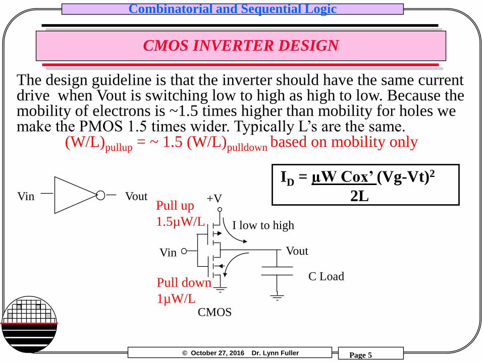
CMOS INVERTER DESIGN
The design guideline is that the inverter should have the same current drive when Vout is switching low to high as high to low. Because the mobility of electrons is ~1.5 times higher than mobility for holes we make the PMOS 1.5 times wider. Typically L’s are the same.
(W/L)pullup = ~ 1.5 (W/L)pulldown based on mobility only
Vin Vout
ID = µW Cox’ (Vg-Vt)2
2LPull up
1.5µW/L
Vin
CMOS
+V
Vout
C Load
I low to high
Pull down
1µW/L

© October 27, 2016 Dr. Lynn Fuller
Combinatorial and Sequential Logic
Page 6
Rochester Institute of Technology
Microelectronic Engineering
CMOS NOR AND NAND
VA VoutVB+V
NANDVA
VB
VAVout
VB+V
NOR
VA VB
3W
W 2W
2W
3W
W
1.5W1.5W
NOR NANDVB
0 0 1 1
0 1 0 1
1 0 0 1
1 1 0 0
VA
The design guideline for other logic gates is to provide the same current drive as the inverter. For the NOR gate we can go from high to low by starting with both inputs at zero and then making either input high or both high. The worst case condition is making only one input high. For that condition we want the same current drive as the inverter. Thus the width of the NMOS should be W. If both the inputs were switching high at the same time the current would be twice as much (that’s okay) For a low to high transition the current goes through two PMOS in series. The equivalent L for the series combination is 2L. If the width for each transistor was 3W the combined value is 3W/2L which is 1.5W/L as desired for equal drive current as the inverter.

© October 27, 2016 Dr. Lynn Fuller
Combinatorial and Sequential Logic
Page 7
Rochester Institute of Technology
Microelectronic Engineering
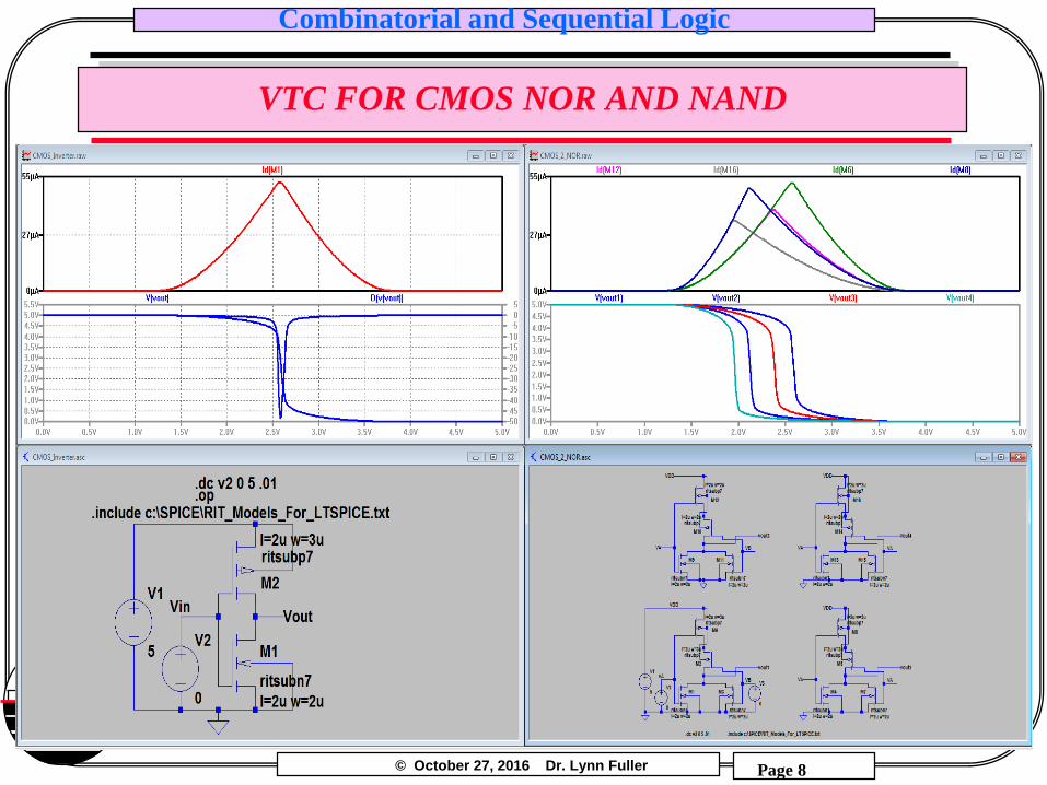
VTC FOR CMOS NOR AND NAND
Vout1 PMOS L=2u, W=3u, VA Sweep 0 to 5, VB=zeroVout2 PMOS L=2u, W=3u, VA Sweep 0 to 5, VB=VAVout3 PMOS L=2u, W=2u, VA Sweep 0 to 5, VB=zeroVout4 PMOS L=2u, W=2u, VA Sweep 0 to 5, VB=VA
NMOSL=2uW=2u
Vout1
Vout2
Vout3
Vout4
© October 27, 2016 Dr. Lynn Fuller
Combinatorial and Sequential Logic
Page 8
Rochester Institute of Technology
Microelectronic Engineering
VTC FOR CMOS NOR AND NAND

© October 27, 2016 Dr. Lynn Fuller
Combinatorial and Sequential Logic
Page 9
Rochester Institute of Technology
Microelectronic Engineering
VTC FOR 3-INPUT NAND
The three NMOS transistors each have different source to substrate voltages which will change the threshold voltage of those transistors and as a result will change the VTC depending on which transistors are switching. This causes a horizontal shift in the VTC.
VA VOUTVB
NAND
VC NANDVB
0 0 0 1
0 0 1 1
0 1 0 1
0 1 1 1
1 0 0 1
1 0 1 1
1 1 0 1
1 1 1 0
VA +V
VA
VB
VC
VOUTM1
M3
M2
© October 27, 2016 Dr. Lynn Fuller
Combinatorial and Sequential Logic
Page 10
Rochester Institute of Technology
Microelectronic Engineering
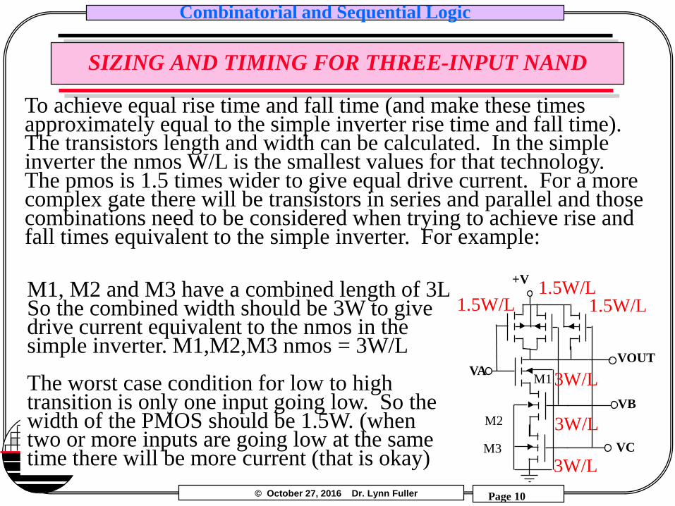
SIZING AND TIMING FOR THREE-INPUT NAND
To achieve equal rise time and fall time (and make these times approximately equal to the simple inverter rise time and fall time). The transistors length and width can be calculated. In the simple inverter the nmos W/L is the smallest values for that technology. The pmos is 1.5 times wider to give equal drive current. For a more complex gate there will be transistors in series and parallel and those combinations need to be considered when trying to achieve rise and fall times equivalent to the simple inverter. For example:
+V
VA
VB
VC
VOUT
M1
M3
M2
M1, M2 and M3 have a combined length of 3LSo the combined width should be 3W to give drive current equivalent to the nmos in the simple inverter. M1,M2,M3 nmos = 3W/L
The worst case condition for low to high transition is only one input going low. So the width of the PMOS should be 1.5W. (when two or more inputs are going low at the same time there will be more current (that is okay)
1.5W/L
3W/L
3W/L
3W/L
1.5W/L1.5W/L

© October 27, 2016 Dr. Lynn Fuller
Combinatorial and Sequential Logic
Page 11
Rochester Institute of Technology
Microelectronic Engineering
3-INPUT NAND
Vout1Vout2
Vout1 has M2 and M3 NMOS on and M1 NMOS switchingVout2 has M1 and M2 NMOS on and M3 NMOS switchingOther combinations are also possible.
+V
VA
VB
VC
VOUTM1
M3
M2
© October 27, 2016 Dr. Lynn Fuller
Combinatorial and Sequential Logic
Page 12
Rochester Institute of Technology
Microelectronic Engineering
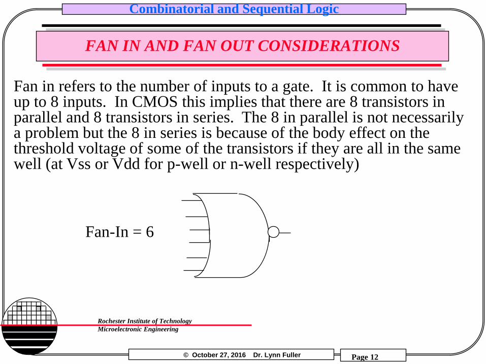
FAN IN AND FAN OUT CONSIDERATIONS
Fan in refers to the number of inputs to a gate. It is common to have up to 8 inputs. In CMOS this implies that there are 8 transistors in parallel and 8 transistors in series. The 8 in parallel is not necessarily a problem but the 8 in series is because of the body effect on the threshold voltage of some of the transistors if they are all in the same well (at Vss or Vdd for p-well or n-well respectively)
Fan-In = 6

© October 27, 2016 Dr. Lynn Fuller
Combinatorial and Sequential Logic
Page 13
Rochester Institute of Technology
Microelectronic Engineering
FAN OUT CONSIDERATIONS
Fan out refers to the number of gates connected to the output of a gate. Each gate adds more capacitance to be charged or discharged during switching which has implications on rise time, fall time and gate delay. The size (W and L) of the MOSFETS can be made to keep the gate delay small.
Fan-Out = 6

© October 27, 2016 Dr. Lynn Fuller
Combinatorial and Sequential Logic
Page 14
Rochester Institute of Technology
Microelectronic Engineering
PSEUDO – CMOS
There are situations where we want a large number of inputs. Rather than have CMOS where there will be many transistors in series (which will not work) we can use a single PMOS/NMOS transistor that is always on.
VIN
CMOS
+V
VO
Idd
VIN
Pseudo CMOS
Inverter
+V
VO
Idd
VA
Pseudo CMOS
4 Input NOR
+V
VO
Idd
VB VC VD

© October 27, 2016 Dr. Lynn Fuller
Combinatorial and Sequential Logic
Page 15
Rochester Institute of Technology
Microelectronic Engineering
OTHER BASIC LOGIC GATES
VAVOUT
VB
VOUTVB
0 0 0 0
0 0 1 0
0 1 0 0
0 1 1 0
1 0 0 0
1 0 1 0
1 1 0 0
1 1 1 1
VAVOUTVOUTVB
0 0 0
0 1 0
1 0 0
1 1 1
VA VB
0 0 0
0 1 1
1 0 1
1 1 1
VA
VB
VAVOUT
ORAND 3 INPUT OR3 INPUT AND
VC VOUTVBVA
0 0 0 0
0 0 1 1
0 1 0 1
0 1 1 1
1 0 0 1
1 0 1 1
1 1 0 1
1 1 1 1
VC
VAVA
VB VBVC VC
VOUT VOUT
© October 27, 2016 Dr. Lynn Fuller
Combinatorial and Sequential Logic
Page 16
Rochester Institute of Technology
Microelectronic Engineering
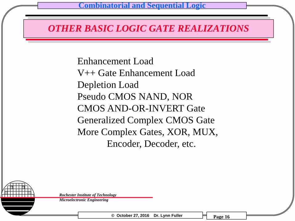
OTHER BASIC LOGIC GATE REALIZATIONS
Enhancement Load
V++ Gate Enhancement Load
Depletion Load
Pseudo CMOS NAND, NOR
CMOS AND-OR-INVERT Gate
Generalized Complex CMOS Gate
More Complex Gates, XOR, MUX,
Encoder, Decoder, etc.

© October 27, 2016 Dr. Lynn Fuller
Combinatorial and Sequential Logic
Page 17
Rochester Institute of Technology
Microelectronic Engineering
GENERALIZED COMPLEX GATE
A
B
C
.
.
A
B
C
.
.
+V Design a gate that provides this output
Network
of PMOS
transistors
Network
of NMOS
transistors
The PMOS network can make the output go high. The NMOS network
can make the output go low. NMOS transistor turn on when the input
goes high while PMOS transistor turn on when the input goes low. The
NMOS and PMOS networks are complementary. Working with the
NMOS network allows you to create a NMOS network that connects the
output low when the appropriate inputs as high (look at what is under the
invert line).
F = (A B) + C
F = (A+B) C
ABC F F
0 0 0 1
0 0 1 1
0 1 0 1
0 1 1 0
1 0 0 1
1 0 1 0
1 1 0 1
1 1 1 0

© October 27, 2016 Dr. Lynn Fuller
Combinatorial and Sequential Logic
Page 18
Rochester Institute of Technology
Microelectronic Engineering
CMOS AND-OR-INVERT GATE
+V
A
BC
VOUT = (A B)+C

© October 27, 2016 Dr. Lynn Fuller
Combinatorial and Sequential Logic
Page 19
Rochester Institute of Technology
Microelectronic Engineering
EXCLUSIVE OR (XOR) DESIGN EXAMPLE
Functional Description – This digital logic circuit returns a true
(high) value when one of two inputs is high and returns a false
(zero) otherwise.
Truth Table
Gate Level Design
VOUTVB
0 0 0
0 1 1
1 0 1
1 1 0
VAExclusive OR
XOR
A
COUT
B

© October 27, 2016 Dr. Lynn Fuller
Combinatorial and Sequential Logic
Page 20
Rochester Institute of Technology
Microelectronic Engineering
GATE LEVEL SIMULATION OF XOR – AND/OR
© October 27, 2016 Dr. Lynn Fuller
Combinatorial and Sequential Logic
Page 21
Rochester Institute of Technology
Microelectronic Engineering
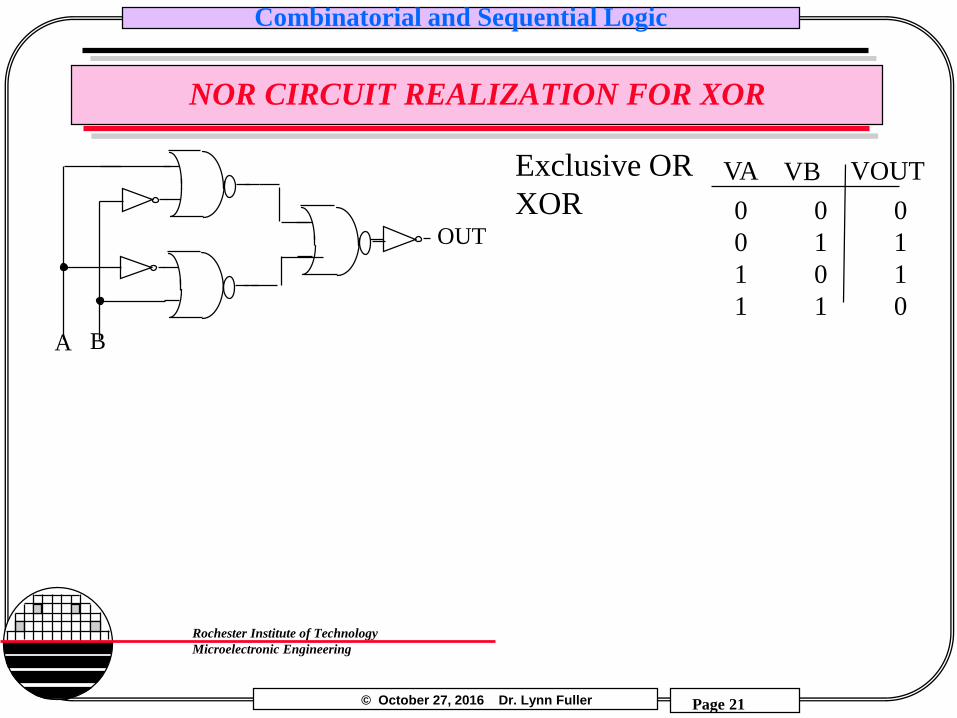
NOR CIRCUIT REALIZATION FOR XOR
VOUTVB
0 0 0
0 1 1
1 0 1
1 1 0
VAExclusive OR
XOROUT
BA

© October 27, 2016 Dr. Lynn Fuller
Combinatorial and Sequential Logic
Page 22
Rochester Institute of Technology
Microelectronic Engineering
GATE LEVEL SIMULATION OF XOR – ALL/NOR

© October 27, 2016 Dr. Lynn Fuller
Combinatorial and Sequential Logic
Page 23
Rochester Institute of Technology
Microelectronic Engineering
TRANSISTOR LEVEL SIMULATION OF XOR – ALL/NOR
18 Transistors

© October 27, 2016 Dr. Lynn Fuller
Combinatorial and Sequential Logic
Page 24
Rochester Institute of Technology
Microelectronic Engineering
XOR CMOS REALIZATION
A
B
C
.
.
A
B
C
.
.
+V
F = (A B)+(A B)
F = (VA+VB) (VA+VB)
+V
A
B
VOUT
B A
B
B
A
12 Transistors
© October 27, 2016 Dr. Lynn Fuller
Combinatorial and Sequential Logic
Page 25
Rochester Institute of Technology
Microelectronic Engineering
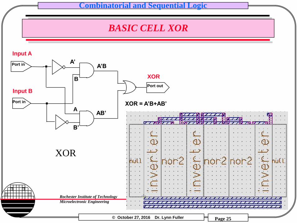
BASIC CELL XOR
Port out
Input A
XOR
Input B
Port in
Port in
XOR = A’B+AB’
A’
B
B’
A
A’B
AB’
XOR

© October 27, 2016 Dr. Lynn Fuller
Combinatorial and Sequential Logic
Page 26
Rochester Institute of Technology
Microelectronic Engineering
LAYOUT FOR XOR

© October 27, 2016 Dr. Lynn Fuller
Combinatorial and Sequential Logic
Page 27
Rochester Institute of Technology
Microelectronic Engineering
BASIC DIGITAL CELLS WITH PADS
Multiplexer XOR Full Adder Encoder Decoder Demux
Edge Triggered D FF
Decoder
JK FF

© October 27, 2016 Dr. Lynn Fuller
Combinatorial and Sequential Logic
Page 28
Rochester Institute of Technology
Microelectronic Engineering
4 TO 1 MULTIPLEXER
I0
I1
I2
I3
Q
A
B

© October 27, 2016 Dr. Lynn Fuller
Combinatorial and Sequential Logic
Page 29
Rochester Institute of Technology
Microelectronic Engineering
4 TO 1 MUX - GATE LEVEL SIMULATION

© October 27, 2016 Dr. Lynn Fuller
Combinatorial and Sequential Logic
Page 30
Rochester Institute of Technology
Microelectronic Engineering
ADDITION IN BINARY
IN BASE 10
7
+2
___
9
IN BINARY
11 CARRY
0111
0010
___
1001 SUM
0 0000
1 0001
2 0010
3 0011
4 0100
5 0101
6 0110
7 0111
8 1000
9 1001
10 1010
11 1011
12 1100
13 1101
14 1110
15 1111
SUM COUTBA
0 0 0 0 0
0 0 1 1 0
0 1 0 1 0
0 1 1 0 1
1 0 0 1 0
1 0 1 0 1
1 1 0 0 1
1 1 1 1 1
CIN
TRUTH TABLE
FOR ADDITION
RULES

© October 27, 2016 Dr. Lynn Fuller
Combinatorial and Sequential Logic
Page 31
Rochester Institute of Technology
Microelectronic Engineering
AND-OR CIRCUIT REALIZATION OF SUM
SUM COUTBA
0 0 0 0 0
0 0 1 1 0
0 1 0 1 0
0 1 1 0 1
1 0 0 1 0
1 0 1 0 1
1 1 0 0 1
1 1 1 1 1
CIN
TRUTH TABLE
FOR ADDITION
RULES
A
SUM
CinB

© October 27, 2016 Dr. Lynn Fuller
Combinatorial and Sequential Logic
Page 32
Rochester Institute of Technology
Microelectronic Engineering
CIRCUIT REALIZATION OF CARRY OUT (COUT)
SUM COUTBA
0 0 0 0 0
0 0 1 1 0
0 1 0 1 0
0 1 1 0 1
1 0 0 1 0
1 0 1 0 1
1 1 0 0 1
1 1 1 1 1
CIN
TRUTH TABLE
FOR ADDITION
RULES
A
COUT
CinB
© October 27, 2016 Dr. Lynn Fuller
Combinatorial and Sequential Logic
Page 33
Rochester Institute of Technology
Microelectronic Engineering
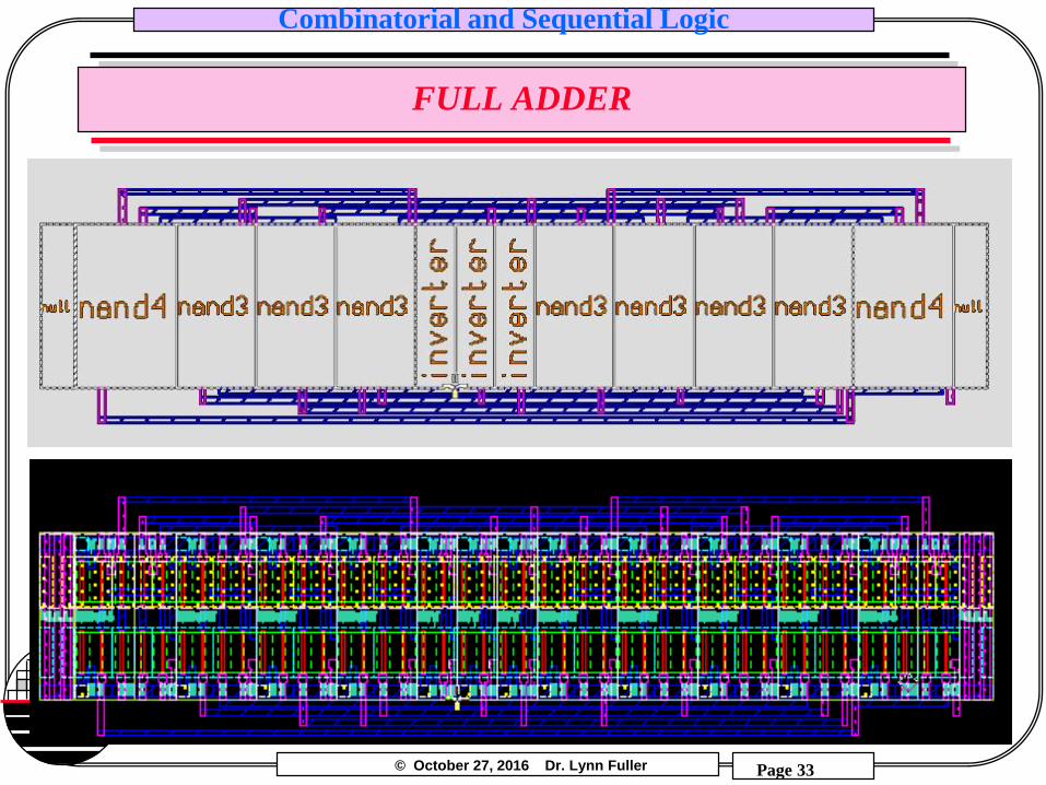
FULL ADDER
© October 27, 2016 Dr. Lynn Fuller
Combinatorial and Sequential Logic
Page 34
Rochester Institute of Technology
Microelectronic Engineering
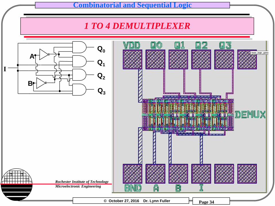
1 TO 4 DEMULTIPLEXER
A
B
I
Q0
Q1
Q2
Q3

© October 27, 2016 Dr. Lynn Fuller
Combinatorial and Sequential Logic
Page 35
Rochester Institute of Technology
Microelectronic Engineering
DECODER
Q0
Q1
Q2
Q3
A
B

© October 27, 2016 Dr. Lynn Fuller
Combinatorial and Sequential Logic
Page 36
Rochester Institute of Technology
Microelectronic Engineering
ENCODER
Q0 Q1
0 0
0 1
1 0
1 1
A B C D
1 0 0 0
0 1 0 0
0 0 1 0
0 0 0 1
Q0Q1Q2
Qn
Coded
Output
Lines
Digital Encoder
512 inputs can be coded into 9 lines
which is a more dramatic benefit
AB
CD
Q1
Q2No Connection

© October 27, 2016 Dr. Lynn Fuller
Combinatorial and Sequential Logic
Page 37
Rochester Institute of Technology
Microelectronic Engineering
FILP-FLOPS
RS FLIP FLOP
QBARS
R Q
D FLIP FLOP
Q
QBARDATA
QS
0 0 Qn-1
0 1 1
1 0 0
1 1 INDETERMINATE
R
Q=DATA IF CLOCK IS HIGH
IF CLOCK IS LOW Q=PREVIOUS DATA VALUE
CLOCK

© October 27, 2016 Dr. Lynn Fuller
Combinatorial and Sequential Logic
Page 38
Rochester Institute of Technology
Microelectronic Engineering
MASTER-SLAVE D FLIP FLOP
DATA
CLOCK
Q
QBAR
NEGATED INPUT NOR IS EQUAL TO AND
B
0 0 1
0 1 1
1 0 0
1 1 0
A OUT
1 1 0
0 1 0
1 1 0
0 0 1
BA OUT
B
=OUT
B
AA
A
B

© October 27, 2016 Dr. Lynn Fuller
Combinatorial and Sequential Logic
Page 39
Rochester Institute of Technology
Microelectronic Engineering
ALL NOR MASTER SLAVE D FLIP FLOP
DATA
CLOCK
Q
DATA
CLOCK
Q
ALL NOR NMOS REALIZATION
ALLOWS FOR LOWER SUPPLY VOLTAGE

© October 27, 2016 Dr. Lynn Fuller
Combinatorial and Sequential Logic
Page 40
Rochester Institute of Technology
Microelectronic Engineering
CMOS CLOCKED DATA LATCH USING AND-OR-INV
CLK
D
Q
_ Q
V D D
C L K
D
Q
C L K _
Q _
D
V D D
© October 27, 2016 Dr. Lynn Fuller
Combinatorial and Sequential Logic
Page 41
Rochester Institute of Technology
Microelectronic Engineering
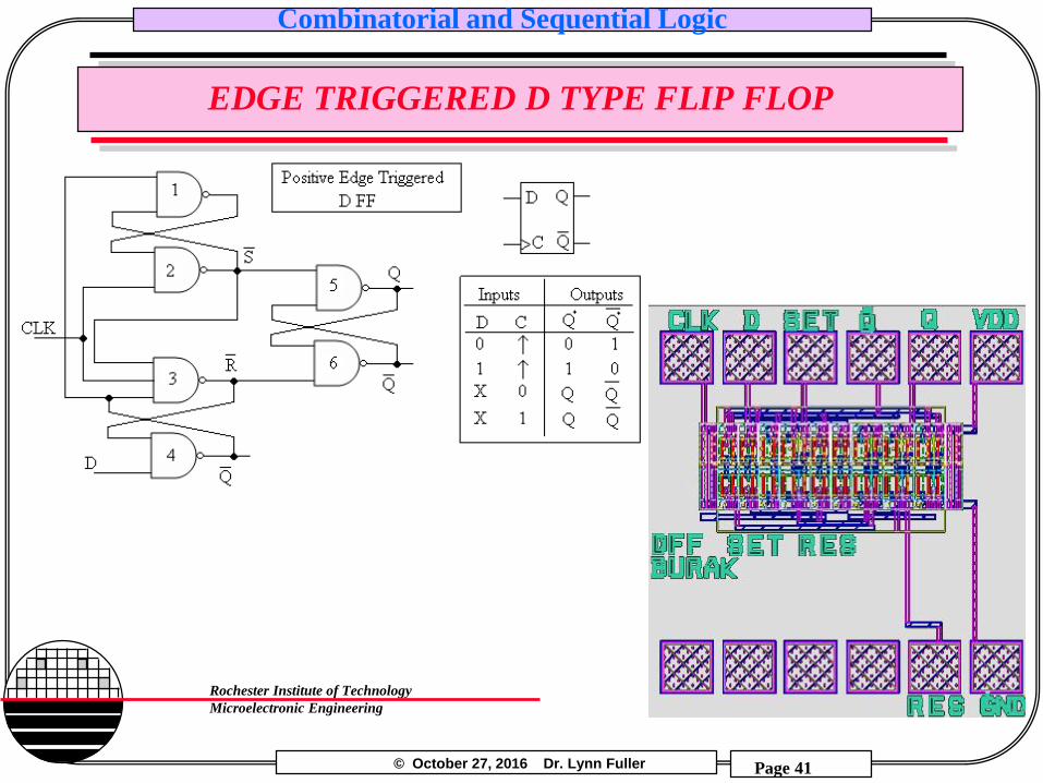
EDGE TRIGGERED D TYPE FLIP FLOP

© October 27, 2016 Dr. Lynn Fuller
Combinatorial and Sequential Logic
Page 42
Rochester Institute of Technology
Microelectronic Engineering
JK FLIP FLOP

© October 27, 2016 Dr. Lynn Fuller
Combinatorial and Sequential Logic
Page 43
Rochester Institute of Technology
Microelectronic Engineering
T-TYPE FILP-FLOP
TOGGEL FLIP FLOP
Q
QBAR
Q: Toggles High and Low with Each Input
QQn-1
0 0 0
0 1 1
1 0 1
1 1 0
T
T

© October 27, 2016 Dr. Lynn Fuller
Combinatorial and Sequential Logic
Page 44
Rochester Institute of Technology
Microelectronic Engineering
BINARY COUNTER USING T TYPE FLIP FLOPS
TOGGEL FLIP FLOP
QQn-1
0 0 0
0 1 1
1 0 1
1 1 0
T
BA
0 0 0 0 0 1 0 0 1
0 0 1 0 1 0 0 1 1
0 1 0 0 1 1 0 0 1
0 1 1 1 0 0 1 1 1
1 0 0 1 0 1 0 0 1
1 0 1 1 1 0 0 1 1
1 1 0 1 1 1 0 0 1
1 1 1 0 0 0 1 1 1
C
State Table for Binary Counter
Present Next F-F
State State InputsBA C TA TB TC
ABC 0 1
00
01
11
10
0
0
0
1 1
0
00
Input
Pulses
TA
ABC 0 1
00
01
11
10
0
1
0
1 1
1
00
TB
ABC 0 1
00
01
11
10
1
1
1
1 1
1
11
TC
A
A
TA
B
B
TB
C
C
Tc
© October 27, 2016 Dr. Lynn Fuller
Combinatorial and Sequential Logic
Page 45
Rochester Institute of Technology
Microelectronic Engineering
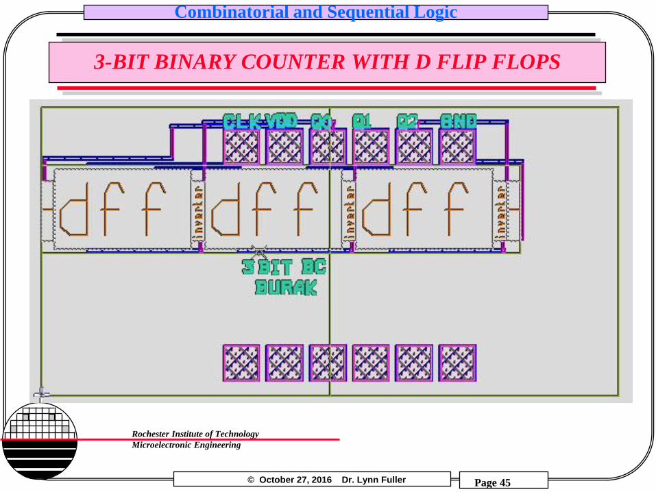
3-BIT BINARY COUNTER WITH D FLIP FLOPS

© October 27, 2016 Dr. Lynn Fuller
Combinatorial and Sequential Logic
Page 46
Rochester Institute of Technology
Microelectronic Engineering
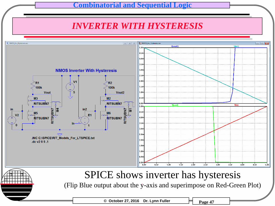
INVERTER WITH HYSTERESIS
1
2
V1
5V
+
-
V2=0-5
Or 5-0
+
-
M1
R=100K
7
3Vout
M3
M2Inverter with Hysteresis
Vin
Vout
The voltage on node 7 is different depending on if Vout is high or low. Changing the Voltage from source to substrate which changes the threshold voltage of M2
© October 27, 2016 Dr. Lynn Fuller
Combinatorial and Sequential Logic
Page 47
Rochester Institute of Technology
Microelectronic Engineering
INVERTER WITH HYSTERESIS
SPICE shows inverter has hysteresis(Flip Blue output about the y-axis and superimpose on Red-Green Plot)

© October 27, 2016 Dr. Lynn Fuller
Combinatorial and Sequential Logic
Page 48
Rochester Institute of Technology
Microelectronic Engineering
RC OSCILLATOR USING INVERTER WITH HYSTERESIS
R
C
RC Oscillator
Vout

© October 27, 2016 Dr. Lynn Fuller
Combinatorial and Sequential Logic
Page 49
Rochester Institute of Technology
Microelectronic Engineering
BUFFERS
R
C
RC Oscillator
VoutVout’
Buffers

© October 27, 2016 Dr. Lynn Fuller
Combinatorial and Sequential Logic
Page 50
Rochester Institute of Technology
Microelectronic Engineering
CMOS INVERTER WITH HYSTERESIS
SPICE show this inverter has hysteresis

© October 27, 2016 Dr. Lynn Fuller
Combinatorial and Sequential Logic
Page 51
Rochester Institute of Technology
Microelectronic Engineering
OSCILLATOR CMOS INVERTER WITH HYSTERESIS
R
CRC Oscillator
Vout

© October 27, 2016 Dr. Lynn Fuller
Combinatorial and Sequential Logic
Page 52
Rochester Institute of Technology
Microelectronic Engineering
REFERNCES
1. Hodges Jackson and Saleh, Analysis and Design of Digital Integrated Circuits, Chapter 4.
2. Sedra and Smith, Microelectronic Circuits, Sixth Edition, Chapter 13.
3. Dr. Fuller’s Lecture Notes, http://people.rit.edu/lffeee

© October 27, 2016 Dr. Lynn Fuller
Combinatorial and Sequential Logic
Page 53
Rochester Institute of Technology
Microelectronic Engineering
HOMEWORK – LOGIC
1. Design a pseudo CMOS NAND gate. Use 1um technology. Show it will work using SPICE.
2. Look up the data sheet for the MM74C14 CMOS inverter with hystersis. Design a 10 Khz oscillator.
3. Use SPICE (transistor level) to simulate the 1 to 4 Demultiplexer.
4. Use SPICE (transistor level) to simulate the positive edge triggered D-type Flip-Flop.
5. Use SPICE to simulate a CMOS RC Oscillator with Buffers.

© October 27, 2016 Dr. Lynn Fuller
Combinatorial and Sequential Logic
Page 54
Rochester Institute of Technology
Microelectronic Engineering
SPICE MODELS FOR CD4007 MOSFETS
*SPICE MODELS FOR RIT DEVICES - DR. LYNN FULLER 8-7-2015*LOCATION DR.FULLER'S WEBPAGE - http://people.rit.edu/lffeee/CMOS.htm**Used in Electronics II for CD4007 inverter chip*Note: Properties L=10u W=170u Ad=8500p As=8500p Pd=440u Ps=440u NRD=0.1 NRS=0.1.MODEL RIT4007N7 NMOS (LEVEL=7+VERSION=3.1 CAPMOD=2 MOBMOD=1+TOX=4E-8 XJ=2.9E-7 NCH=4E15 NSUB=5.33E15 XT=8.66E-8 +VTH0=1.4 U0= 1300 WINT=2.0E-7 LINT=1E-7 +NGATE=5E20 RSH=300 JS=3.23E-8 JSW=3.23E-8 CJ=6.8E-8 MJ=0.5 PB=0.95+CJSW=1.26E-10 MJSW=0.5 PBSW=0.95 PCLM=5+CGSO=3.4E-10 CGDO=3.4E-10 CGBO=5.75E-10)**Used in Electronics II for CD4007 inverter chip*Note: Properties L=10u W=360u Ad=18000p As=18000p Pd=820u Ps=820u NRS=O.54 NRD=0.54.MODEL RIT4007P7 PMOS (LEVEL=7+VERSION=3.1 CAPMOD=2 MOBMOD=1+TOX=5E-8 XJ=2.26E-7 NCH=1E15 NSUB=8E14 XT=8.66E-8+VTH0=-1.65 U0= 400 WINT=1.0E-6 LINT=1E-6+NGATE=5E20 RSH=1347 JS=3.51E-8 JSW=3.51E-8 CJ=5.28E-8 MJ=0.5 PB=0.94+CJSW=1.19E-10 MJSW=0.5 PBSW=0.94 pCLM=5+CGSO=4.5E-10 CGDO=4.5E-10 CGBO=5.75E-10)

© October 27, 2016 Dr. Lynn Fuller
Combinatorial and Sequential Logic
Page 55
Rochester Institute of Technology
Microelectronic Engineering
SPICE MODELS FOR MOSFETS
* From Sub-Micron CMOS Manufacturing Classes in MicroE ~ 1um Technology
.MODEL RITSUBN7 NMOS (LEVEL=7
+VERSION=3.1 CAPMOD=2 MOBMOD=1
+TOX=1.5E-8 XJ=1.84E-7 NCH=1.45E17 NSUB=5.33E16 XT=8.66E-8
+VTH0=1.0 U0= 600 WINT=2.0E-7 LINT=1E-7
+NGATE=5E20 RSH=1082 JS=3.23E-8 JSW=3.23E-8 CJ=6.8E-4 MJ=0.5 PB=0.95
+CJSW=1.26E-10 MJSW=0.5 PBSW=0.95 PCLM=5
+CGSO=3.4E-10 CGDO=3.4E-10 CGBO=5.75E-10)
*
*From Sub-Micron CMOS Manufacturing Classes in MicroE ~ 1um Technology
.MODEL RITSUBP7 PMOS (LEVEL=7
+VERSION=3.1 CAPMOD=2 MOBMOD=1
+TOX=1.5E-8 XJ=2.26E-7 NCH=7.12E16 NSUB=3.16E16 XT=8.66E-8
+VTH0=-1.0 U0= 376.72 WINT=2.0E-7 LINT=2.26E-7
+NGATE=5E20 RSH=1347 JS=3.51E-8 JSW=3.51E-8 CJ=5.28E-4 MJ=0.5 PB=0.94
+CJSW=1.19E-10 MJSW=0.5 PBSW=0.94
+CGSO=4.5E-10 CGDO=4.5E-10 CGBO=5.75E-10)

© October 27, 2016 Dr. Lynn Fuller
Combinatorial and Sequential Logic
Page 56
Rochester Institute of Technology
Microelectronic Engineering
SPICE MODELS FOR MOSFETS
*4-4-2013 LTSPICE uses Level=8
* From Electronics II EEEE482 FOR ~100nm Technology
.model EECMOSN NMOS (LEVEL=8
+VERSION=3.1 CAPMOD=2 MOBMOD=1
+TOX=5E-9 XJ=1.84E-7 NCH=1E17 NSUB=5E16 XT=5E-8
+VTH0=0.4 U0= 200 WINT=1E-8 LINT=1E-8
+NGATE=5E20 RSH=1000 JS=3.23E-8 JSW=3.23E-8 CJ=6.8E-4 MJ=0.5 PB=0.95
+CJSW=1.26E-10 MJSW=0.5 PBSW=0.95 PCLM=5
+CGSO=3.4E-10 CGDO=3.4E-10 CGBO=5.75E-10)
*
*4-4-2013 LTSPICE uses Level=8
* From Electronics II EEEE482 FOR ~100nm Technology
.model EECMOSP PMOS (LEVEL=8
+TOX=5E-9 XJ=0.05E-6 NCH=1E17 NSUB=5E16 XT=5E-8
+VTH0=-0.4 U0= 100 WINT=1E-8 LINT=1E-8
+NGATE=5E20 RSH=1000 JS=3.51E-8 JSW=3.51E-8 CJ=5.28E-4 MJ=0.5 PB=0.94
+CJSW=1.19E-10 MJSW=0.5 PBSW=0.94 PCLM=5
+CGSO=4.5E-10 CGDO=4.5E-10 CGBO=5.75E-10)
*