communication architecture design for reconfigurable multimedia soc platform
TRANSCRIPT

Des Autom Embed Syst (2010) 14: 1–20DOI 10.1007/s10617-009-9048-0
Communication architecture design for reconfigurablemultimedia SoC platform
Ganghee Lee · Yongjin Ahn · Seokhyun Lee ·Jeongki Son · Kiwook Yoon · Kiyoung Choi
Received: 2 April 2008 / Accepted: 28 September 2009 / Published online: 11 November 2009© Springer Science+Business Media, LLC 2009
Abstract Memory and communication architecture have a significant impact on the perfor-mance, cost, and power of complex multiprocessor system-on-chip designs. In this paper, wepresent an automated bus matrix synthesis flow for efficient transaction-level design spaceexploration of communication architecture in a reconfigurable multimedia system-on-chipplatform. Specifically, we consider hardware interface selection problem, which has sig-nificant effect on the overall cost of area and power. We propose a method to solve suchhardware interface selection problem through static analysis of communication behavior.We experiment with JPEG encoder and H.264 encoder examples and the results show thereduction of area by 56.91% and power by 48.61% of bus matrix with 0.58% performanceoverhead on average compared to the case of maximum performance. According to our HWinterface selection algorithm, we also experiment MPEG4 video decoder example. And theresult is evaluated on the FPGA prototyping board.
Keywords Multiprocessor system-on-chip · Transaction level model · Coarse-grainedreconfigurable architecture · Schedule · Design space exploration
G. Lee (�) · Y. Ahn · S. Lee · J. Son · K. ChoiSeoul National University, Seoul, South Koreae-mail: [email protected]
Y. Ahne-mail: [email protected]
S. Leee-mail: [email protected]
J. Sone-mail: [email protected]
K. Choie-mail: [email protected]
K. YoonSoft development division, CORELOGIC Ltd., Seoul, South Koreae-mail: [email protected]
2 G. Lee et al.
1 Introduction
As billion transistors system-on-chip (SoC) design becomes a reality, the productivity gapbetween rapidly increasing design complexity and designer productivity lagging behind isbecoming a more serious problem to be solved [32]. To reduce the gap, it is a current trendto move the focus toward higher levels of abstraction [14]. The designer starts with a veryabstract mathematical model such as a process network or a finite state machine, and then themodel is refined step by step to lower levels of abstraction before the final implementationis obtained [1]. Each refinement step typically requires generating an executable model forsimulation to validate the refined design, which is a cumbersome and error-prone process ifit is done manually. Another method to reduce the productivity gap is intellectual property(IP) reuse. Designing parameterized IP cores [10] with a well defined interface [28] allowscores to be quickly customized and integrated in multiple design projects. The VSIA [34]and OCP-IP [24] standards have produced specifications of interfaces.
Among many parameters used for customizing an IP core, we focus in this paper on theparameter that determines whether the core is to be implemented as a master or a slave. Ifmore IP cores are implemented as masters, communication concurrency will be improved(we assume that multiple communications can occur concurrently through multiple busesand a crossbar switch). However, adding too many masters causes a complex communi-cation system requiring unnecessary area overhead. If IP cores are implemented as slaves,all their communications can be accomplished by one master or Direct Memory Access(DMA) module, thereby minimizing the cost. Therefore, we need to find an optimal pointwhere some cores get master interface and others get slave interface so that we can achievemaximal performance at minimal area cost. This is what we call hardware (HW) interfaceselection problem. In a previous paper [18], we presented an automated bus matrix synthe-sis flow including transaction-level code generation, HW interface selection, synthesis ofthe interface, and simulation.
General purpose processors are in general flexible enough to support various applica-tions, and fit well with various demands of the customers. But they may not provide suffi-cient performance to cope with the complexity of the applications. On the other hand, Ap-plication Specific Integrated Circuits (ASICs) are good at performance but have little flex-ibility. To achieve both performance and flexibility, recent researchers have considered re-configurable architecture. Generally there are two kinds of reconfigurable architecture: fine-grained [6] and coarse-grained [15]. Our platform embeds a coarse-grained ReconfigurableComputing Module (RCM), since the fine-grained one requires long latency for reconfigura-tion. In this paper, we introduce an extended bus matrix synthesis flow with coarse-grainedreconfiguration architecture. The result is demonstrated on FPGA with MPEG4 video de-coder example.
1.1 Backgrounds
In this section, we present previous researches in on-chip communication architecture designas well as the coarse-grained reconfigurable architecture that we are adopting.
1.1.1 On-chip communication architecture design
Many leading research groups have been studying memory and communication architec-tures. Hierarchical shared bus communication architectures such as those proposed by
Communication architecture design for reconfigurable multimedia 3
AMBA [4], CoreConnect [13], and STBus [30] can connect few tens of IPs in a cost-effective manner but are not scalable to cope with the demands of modern MultiProces-sor SoC (MPSoC). Network-on-Chip (NoC) communication architectures [8] have emergedas a promising alternative to handle communication needs for the next generation of high-performance designs, but it fits better with rather larger chips with hundreds of IPs. Sowe believe that multi-layered bus matrix [22] is currently the most practical way of realiz-ing concurrent communications among tens of modules from the viewpoint of performanceand area. Ogawa et al. [23] have proposed a transaction-based simulation environment thatallows designers to explore and design a bus matrix. But the designer needs to manuallyspecify the communication topology, which is too time-consuming for today’s complex sys-tems. Automated synthesis approaches such as STBus crossbar [21], AXI-based bus matrix[25–27], and cascaded bus matrix [36] have been proposed, but their analysis does not con-sider the HW interface synthesis and the relationship with DMA.
Our design flow is based on SoCDAL [2] (System-on-Chip Design AcceLerator) whichhas been developed for efficient SoC design space exploration. We start from the mappingresult of SoCDAL, and refine the communication architecture considering HW interface.
1.1.2 Coarse-grained reconfigurable architecture
Recently, many researchers have suggested coarse-grained reconfigurable architectures suchas Morphosys, XPP, and ADRES [7, 19, 29]. A typical coarse-grained reconfigurable archi-tecture consists of a general purpose processor for executing irregular code segments anda Reconfigurable Computing Module (RCM) for executing computation-intensive regularcode segments, and these execution units are connected with a shared bus.
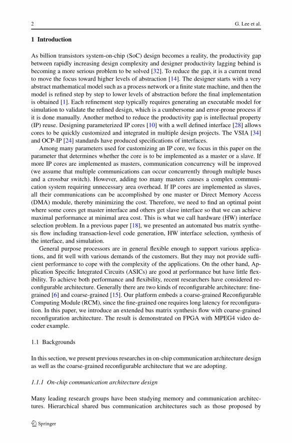
The RCM used in our platform consists of an array of processing elements (PEs), severalsets of frame buffers, and a configuration cache memory [15]. Figure 1 shows the typicalstructure of the RCM. In the PE array, each PE can be dynamically reconfigured to performarithmetic and logical operations. It is connected with the nearest neighboring PEs-top, bot-tom, left, and right. Frame buffer is used for storing the data and it consists of two sets ofmemory each of which consists of three banks: one connected to the write bus and the othertwo connected to the read buses. Any of the three banks can be connected to any of theread or write buses. The configuration cache is composed of spatial Cache Elements (CEs),temporal CEs, and a cache controller for controlling each of the CE. Each CE has severallayers so that each PE can be reconfigured independently with different contexts. The hybridstructure of configuration cache combining spatial cache and temporal cache helps reducingpower consumption without degrading performance [16].
1.2 Contributions
We propose an efficient communication architecture design methodology that includes HWinterface selection. The HW interface selection is based on the previous paper [18], butin this paper: (i) we modify the algorithm which includes extensions to support coarse-grained RCM and add experimental results obtained by this modified algorithm, (ii) we addthe power aspect along with the performance and area in the experimental results, (iii) toevaluate our results, we prototype our coarse-grained reconfigurable architect on FPGA withMPEG4 video decoder example.
4 G. Lee et al.
Fig. 1 Typical structure of the reconfigurable computing module
1.3 Paper organization
The remainder of this paper is organized as follows. In Sect. 2, we briefly introduce our SoCdesign flow and target platform. In Sect. 3, we explain the method for efficient bus matrixdesign based on HW interface selection. In Sect. 4, we show some experimental resultswith JPEG encoder, H.264 encoder, and MPEG4 video decoder examples. Especially wepresent the FPGA prototyping of an MPEG4 video decoder example through the proposedapproach. Finally, we conclude with some remarks on future work in Sect. 5.
2 SoC design flow and target platform
In this section, we describe our SoC design flow and target platform. The design flow isbased on an existing design environment called SoCDAL [2]. In this work, we add severalnew features to it and extend the target platform with RCM.
2.1 SoCDAL (System-on-Chip AcceLerator)
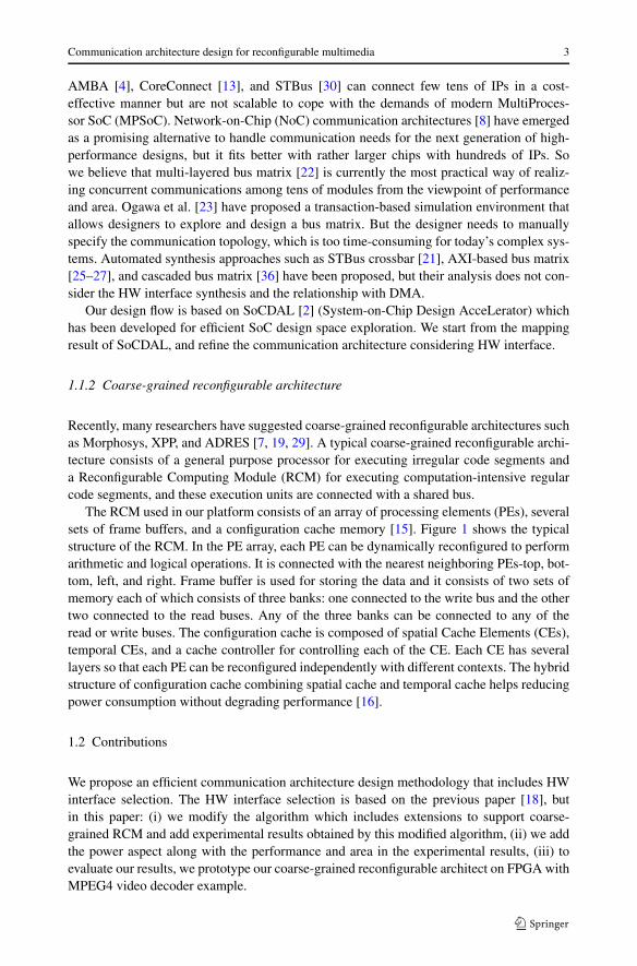
Figure 2 shows the overall design flow of SoCDAL. From a process network model in Sys-temC [31], it generates a hierarchical model consisting of Synchronous Data Flow (SDF)models and Finite State Machines (FSMs) using an automatic conversion tool. The conver-sion tool forks into two paths. In one path, it parses the input SystemC files using Lex/Yacc
Communication architecture design for reconfigurable multimedia 5
Fig. 2 Overall design flow of SoCDAL
to extract the connection information of ports between processes. In the other path, it extractsthe behavior from the SystemC files and generates the corresponding C files, and then, fromthese results, the conversion tool generates a model composed hierarchically of FSM graphsand SDF graphs through control/data flow analysis using SUIF1 compiler [33].
The hierarchical model graph and C codes are the inputs to static SW/HW estimation.For SW estimation, it compiles the generated C codes, generates an executable image andgenerates a basic block graph through control flow analysis. And then it generates a set ofInteger Linear Programming (ILP) formulas and solves it with an ILP solver to obtain worstcase execution time. The estimated results are annotated into the hierarchical model. ForHW estimation, it generates Control Data Flow Graph (CDFG) from C codes using SUIF1.Initially, the C codes are optimized through basic SUIF1 optimization and further optimizedin the form of the generated CDFGs, including constant folding and common subexpres-sion elimination. Then it performs high-level synthesis on the generated CDFGs to obtainsynthesized CDFGs (CDFGs annotated with the synthesis results). From the synthesizedCDFGs, it generates a set of ILP formulas and solves it with an ILP solver in the same wayas SW estimation.
The estimated results are also annotated into the hierarchical model and used to map theapplication to the target architecture. To estimate the performance of the whole system, itschedules the system statically. At this stage, it also tries to minimize the buffer size whileavoiding deadlock problem.
The mapping tool takes the hierarchical model and target architecture information whichcontains processor allocation, bus architecture, communication overhead, OS information,and so on. It maps actors to the target architecture using an extended version of quantum-inspired evolutionary algorithm [11] with the cost function of performance, area, and power.Finally, it synthesizes codes to be executed on processors or hard-wired logics accordingto the mapping result, and then we validate the system by simulation at various levels ofabstraction such as transaction level, bus-cycle-accurate level, etc. Refer to [2] for the detailsof SoCDAL.
6 G. Lee et al.
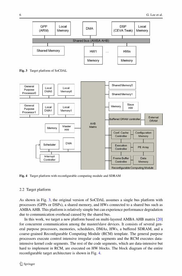
Fig. 3 Target platform of SoCDAL
Fig. 4 Target platform with reconfigurable computing module and SDRAM
2.2 Target platform
As shown in Fig. 3, the original version of SoCDAL assumes a single bus platform withprocessors (GPPs or DSPs), a shared memory, and HWs connected to a shared bus such asAMBA AHB. This platform is relatively simple but can experience performance degradationdue to communication overhead caused by the shared bus.
In this work, we target a new platform based on multi-layered AMBA AHB matrix [20]for concurrent communication among the master/slave devices. It consists of several gen-eral purpose processors, memories, schedulers, DMAs, HWs, a buffered SDRAM, and acoarse-grained Reconfigurable Computing Module (RCM) template. The general purposeprocessors execute control intensive irregular code segments and the RCM executes data-intensive kernel code segments. The rest of the code segments, which are data-intensive buthard to implement in RCM, are executed on HW blocks. The block diagram of the entirereconfigurable target architecture is shown in Fig. 4.

Communication architecture design for reconfigurable multimedia 7
Fig. 5 Communicationarchitecture design flow
3 Communication architecture design
In this section, we explain the proposed methodology for communication architecture designwith HW interface selection. Figure 5 shows the overall flow of the communication archi-tecture design integrated into SoCDAL. For the communication architecture, it synthesizesa priority-based bus matrix like multi-layered AHB. In this paper, among many design prob-lems to be solved for synthesizing the optimized bus matrix, we focus on interface selectionproblem.
3.1 Timed functional SystemC model generation and simulation
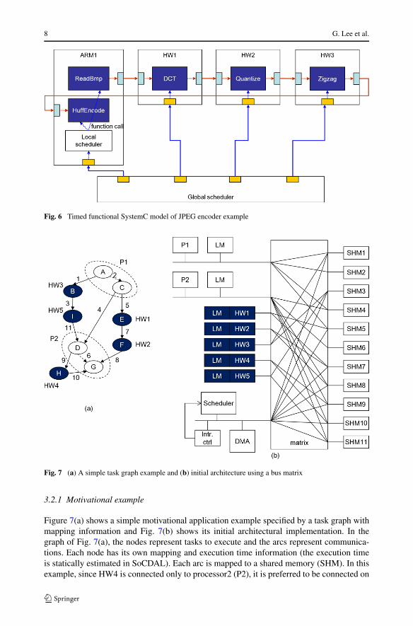
As show in Fig. 5, from the given mapping and scheduling result from SoCDAL, we firstgenerate timed functional SystemC (TFSC) codes. Figure 6 shows TFSC model of JPEGencoder example. These codes are used for extracting communication information, as wellas quickly evaluating the mapping and scheduling results obtained in the prior design stage.The TFSC codes run with static scheduling which is given from SoCDAL. There is a globalscheduler which schedules all the components. If the computing module must run severaltasks, (which means that the module is processor or reconfigurable computing module) weput local scheduler, where using a function call mechanism. The communication mechanismamong the modules is FIFO in SystemC. The module executes the tasks when the data isready and received a signal from the scheduler. We get communication conflict informationfrom this TFSC model generation and simulation.
3.2 Bus matrix synthesis
In the stage of bus matrix synthesis, we map logical communication channels of TFSCcodes to physical buses in optimized bus matrix architecture. In addition to applying existingtechniques [1, 17, 27, 35] for the optimization of the bus matrix architecture, we apply ourown HW interface selection technique to further improve the architecture, which is the mainfocus of this subsection.
8 G. Lee et al.
Fig. 6 Timed functional SystemC model of JPEG encoder example
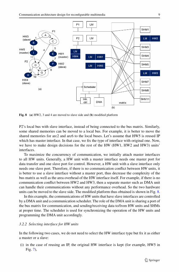
Fig. 7 (a) A simple task graph example and (b) initial architecture using a bus matrix
3.2.1 Motivational example
Figure 7(a) shows a simple motivational application example specified by a task graph withmapping information and Fig. 7(b) shows its initial architectural implementation. In thegraph of Fig. 7(a), the nodes represent tasks to execute and the arcs represent communica-tions. Each node has its own mapping and execution time information (the execution timeis statically estimated in SoCDAL). Each arc is mapped to a shared memory (SHM). In thisexample, since HW4 is connected only to processor2 (P2), it is preferred to be connected on
Communication architecture design for reconfigurable multimedia 9
Fig. 8 (a) HW2, 3 and 4 are moved to slave side and (b) modified platform
P2’s local bus with slave interface, instead of being connected to the bus matrix. Similarly,some shared memories can be moved to a local bus. For example, it is better to move theshared memories for arc2 and arc6 to the local buses. Let’s assume that HW5 is reused IPwhich has master interface. In that case, we fix the type of interface with original one. Now,we have to make design decisions for the rest of the HW (HW1, HW2 and HW3) units’interfaces.
To maximize the concurrency of communication, we initially attach master interfacesto all HW units. Generally, a HW unit with a master interface needs one master port fordata transfer and one slave port for control. However, a HW unit with a slave interface onlyneeds one slave port. Therefore, if there is no communication conflict between HW units, itis better to use a slave interface without a master port, thus decrease the complexity of thebus matrix as well as the area overhead of the HW interface itself. For example, if there is nocommunication conflict between HW2 and HW3, then a separate master such as DMA unitcan handle their communications without any performance overhead. So the two hardwareunits can be moved to the slave side. The modified platform thus obtained is shown in Fig. 8.
In this example, the communications of HW units that have slave interfaces are controlledby a DMA unit and a communication scheduler. The role of the DMA unit is sharing a port ofthe bus matrix for communication, and sending/receiving data to/from HW units and SHMsat proper time. The scheduler is used for synchronizing the operation of the HW units andprogramming the DMA unit accordingly.
3.2.2 Selecting interface for HW units
In the following two cases, we do not need to select the HW interface type but fix it as eithera master or a slave:
(i) in the case of reusing an IP, the original HW interface is kept (for example, HW5 inFig. 7),
10 G. Lee et al.
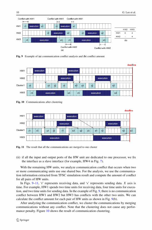
Fig. 9 Example of (a) communication conflict analysis and (b) conflict amount
Fig. 10 Communications after clustering
Fig. 11 The result that all the communications are merged to one cluster
(ii) if all the input and output ports of the HW unit are dedicated to one processor, we fixthe interface as a slave interface (for example, HW4 in Fig. 7).
With the remaining HW units, we analyze communication conflict that occurs when twoor more communicating units use one shared bus. For the analysis, we use the communica-tion information extracted from TFSC simulation result and compute the amount of conflictfor all pairs of HW units.
In Figs. 9–11, ‘r’ represents receiving data, and ‘s’ represents sending data. X axis istime. For example, HW1 spends two time units for receiving data, four time units for execu-tion, and two time units for sending data. In the example of Fig. 9, there is no communicationconflict between HW1 and HW2 but HW3 has conflicts with the other two units. We cancalculate the conflict amount for each pair of HW units as shown in Fig. 9(b).
After analyzing the communication conflict, we cluster the communications by mergingcommunications without any conflict. Note that the clustering does not cause any perfor-mance penalty. Figure 10 shows the result of communication clustering.
Communication architecture design for reconfigurable multimedia 11
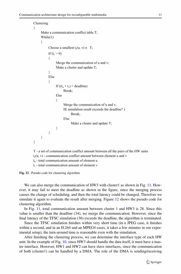
Fig. 12 Pseudo code for clustering algorithm
We can also merge the communication of HW3 with cluster1 as shown in Fig. 11. How-ever, it may fail to meet the deadline as shown in the figure, since the merging processcauses the change of scheduling, and then the total latency could be changed. Therefore wesimulate it again to evaluate the result after merging. Figure 12 shows the pseudo code forclustering algorithm.
In Fig. 11, total communication amount between cluster 1 and HW3 is 28. Since thisvalue is smaller than the deadline (34), we merge the communication. However, since thefinal latency of the TFSC simulation (36) exceeds the deadline, the algorithm is terminated.
Since the TFSC simulation finishes within very short time (in a JPEG case, it finisheswithin a second, and in an H.264 and an MPEG4 cases, it takes a few minutes in our exper-imental setup), the turn-around time is reasonable even with the simulation.
After finishing the clustering process, we can determine the interface type of each HWunit. In the example of Fig. 10, since HW3 should handle the data itself, it must have a mas-ter interface. However, HW1 and HW2 can have slave interfaces, since the communicationof both (cluster1) can be handled by a DMA. The role of the DMA is sending/receiving
12 G. Lee et al.
data to/from the HW units at proper time. The number of necessary DMA is the numberof clusters. Since each DMA has to handle several HW units which have slave interfaces,scheduling is required. The schedule of services for multiple DMA requests is automaticallygenerated by the order of communication in a cluster. For the schedule of services for mul-tiple DMA requests, we apply first-come first-served policy and if multiple requests takeplace at the same time, then we serve them according to the priority. The user can set thepriority of each HW unit. In our algorithm, the task which has prior data dependency getshigher priority.
Since our algorithm is targeting real time systems design, it guarantees meeting the dead-line. However it does not guarantee optimum solution. It generates an efficient communica-tion architecture which meets the performance constraint with minimal area and power.
3.2.3 Design problems and solutions in the extended platform
An RCM can be reused again and again to execute different tasks by just reconfiguring it.Since the reconfiguration has little overhead (takes only one cycle), task switching can bedone on the fly during the execution of the application. Mapping more tasks on the RCMdoes not increase the area cost provided that their executions are scheduled properly.1 So anRCM can be treated much like a processor running SW, even though it achieves HW-likeperformance through parallelism. So we try to map as many computation-intensive tasks aspossible on the RCM.
We extend our HW interface selection algorithm with this extended platform which hasan RCM. In our algorithm, the RCM is treated as special HW which acts like a processor.Since the behavior of the processor is already implemented in our TFSC model, there is nooverhead of implementing the behavior of the RCM in the TFSC model. Once the TFSCmodel is given, the remaining steps for synthesizing the communication architecture are thesame.
3.3 Bus cycle accurate model generation and simulation
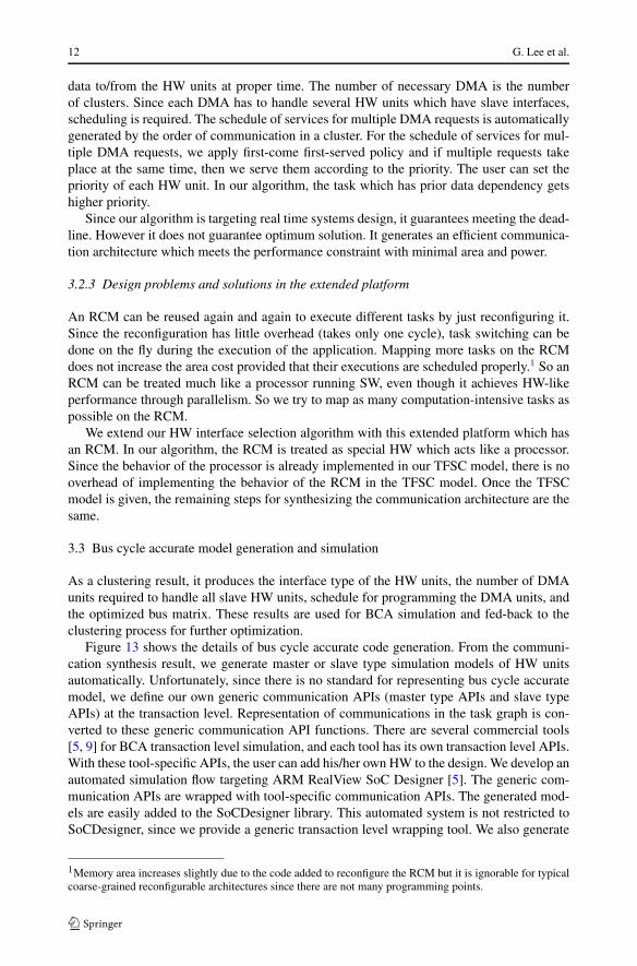
As a clustering result, it produces the interface type of the HW units, the number of DMAunits required to handle all slave HW units, schedule for programming the DMA units, andthe optimized bus matrix. These results are used for BCA simulation and fed-back to theclustering process for further optimization.
Figure 13 shows the details of bus cycle accurate code generation. From the communi-cation synthesis result, we generate master or slave type simulation models of HW unitsautomatically. Unfortunately, since there is no standard for representing bus cycle accuratemodel, we define our own generic communication APIs (master type APIs and slave typeAPIs) at the transaction level. Representation of communications in the task graph is con-verted to these generic communication API functions. There are several commercial tools[5, 9] for BCA transaction level simulation, and each tool has its own transaction level APIs.With these tool-specific APIs, the user can add his/her own HW to the design. We develop anautomated simulation flow targeting ARM RealView SoC Designer [5]. The generic com-munication APIs are wrapped with tool-specific communication APIs. The generated mod-els are easily added to the SoCDesigner library. This automated system is not restricted toSoCDesigner, since we provide a generic transaction level wrapping tool. We also generate
1Memory area increases slightly due to the code added to reconfigure the RCM but it is ignorable for typicalcoarse-grained reconfigurable architectures since there are not many programming points.
Communication architecture design for reconfigurable multimedia 13
Fig. 13 The details of bus cycle accurate model
C codes for SW part to be executed on ISS’s. The generated C codes contain a functioncall based static scheduler. The schedule includes programming DMA units. Finally, theevaluation results are fed-back to the mapping stage to find a better solution.
4 Experimental results
4.1 Experiments
In this section, we experiment with JPEG encoder, H.264 encoder, and MPEG4 video de-coder examples for HW interface selection problem. The results are evaluated with com-mercial transaction-level tool.
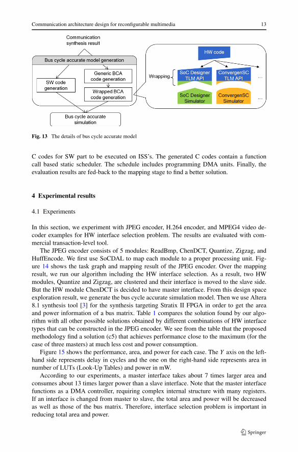
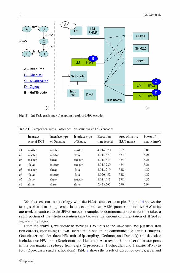
The JPEG encoder consists of 5 modules: ReadBmp, ChenDCT, Quantize, Zigzag, andHuffEncode. We first use SoCDAL to map each module to a proper processing unit. Fig-ure 14 shows the task graph and mapping result of the JPEG encoder. Over the mappingresult, we run our algorithm including the HW interface selection. As a result, two HWmodules, Quantize and Zigzag, are clustered and their interface is moved to the slave side.But the HW module ChenDCT is decided to have master interface. From this design spaceexploration result, we generate the bus cycle accurate simulation model. Then we use Altera8.1 synthesis tool [3] for the synthesis targeting Stratix II FPGA in order to get the areaand power information of a bus matrix. Table 1 compares the solution found by our algo-rithm with all other possible solutions obtained by different combinations of HW interfacetypes that can be constructed in the JPEG encoder. We see from the table that the proposedmethodology find a solution (c5) that achieves performance close to the maximum (for thecase of three masters) at much less cost and power consumption.
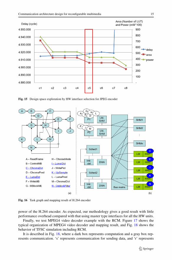
Figure 15 shows the performance, area, and power for each case. The Y axis on the left-hand side represents delay in cycles and the one on the right-hand side represents area innumber of LUTs (Look-Up Tables) and power in mW.
According to our experiments, a master interface takes about 7 times larger area andconsumes about 13 times larger power than a slave interface. Note that the master interfacefunctions as a DMA controller, requiring complex internal structure with many registers.If an interface is changed from master to slave, the total area and power will be decreasedas well as those of the bus matrix. Therefore, interface selection problem is important inreducing total area and power.
14 G. Lee et al.
Fig. 14 (a) Task graph and (b) mapping result of JPEG encoder
Table 1 Comparison with all other possible solutions of JPEG encoder
Interface Interface type Interface type Execution Area of matrix Power of
type of DCT of Quantize of Zigzag time (cycle) (LUT num.) matrix (mW)
c1 master master master 4,914,870 717 7.80
c2 master master slave 4,915,573 424 5.26
c3 master slave master 4,915,644 424 5.26
c4 slave master master 4,915,789 424 5.26
c5 master slave slave 4,918,219 338 4.32
c6 slave master slave 4,920,452 338 4.32
c7 slave slave master 4,918,945 338 4.32
c8 slave slave slave 5,429,563 230 2.94
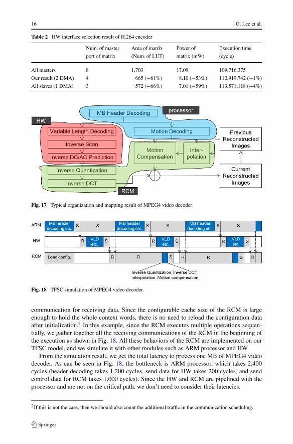
We also test our methodology with the H.264 encoder example. Figure 16 shows thetask graph and mapping result. In this example, two ARM processors and five HW unitsare used. In contrast to the JPEG encoder example, its communication conflict time takes asmall portion of the whole execution time because the amount of computation of H.264 issignificantly larger.
From the analysis, we decide to move all HW units to the slave side. We put them intotwo clusters, each using its own DMA unit, based on the communication conflict analysis.One cluster includes three HW units (Upsampling, Dctluma, and Deblock) and the otherincludes two HW units (Dctchroma and Idctluma). As a result, the number of master portsin the bus matrix is reduced from eight (2 processors, 1 scheduler, and 5 master HWs) tofour (2 processors and 2 schedulers). Table 2 shows the result of execution cycles, area, and
Communication architecture design for reconfigurable multimedia 15
Fig. 15 Design space exploration by HW interface selection for JPEG encoder
Fig. 16 Task graph and mapping result of H.264 encoder
power of the H.264 encoder. As expected, our methodology gives a good result with littleperformance overhead compared with that using master type interfaces for all the HW units.
Finally, we test MPEG4 video decoder example with the RCM. Figure 17 shows thetypical organization of MPEG4 video decoder and mapping result, and Fig. 18 shows thebehavior of TFSC simulation including RCM.
It is described in Fig. 18, where a dark box represents computation and a gray box rep-resents communication. ‘s’ represents communication for sending data, and ‘r’ represents
16 G. Lee et al.
Table 2 HW interface selection result of H.264 encoder
Num. of master Area of matrix Power of Execution time
port of matrix (Num. of LUT) matrix (mW) (cycle)
All masters 8 1,703 17.09 109,716,375
Our result (2 DMA) 4 665 (−61%) 8.10 (−53%) 110,919,742 (+1%)
All slaves (1 DMA) 3 572 (−66%) 7.01 (−59%) 113,571,118 (+4%)
Fig. 17 Typical organization and mapping result of MPEG4 video decoder
Fig. 18 TFSC simulation of MPEG4 video decoder
communication for receiving data. Since the configurable cache size of the RCM is largeenough to hold the whole context words, there is no need to reload the configuration dataafter initialization.2 In this example, since the RCM executes multiple operations sequen-tially, we gather together all the receiving communications of the RCM in the beginning ofthe execution as shown in Fig. 18. All these behaviors of the RCM are implemented on ourTFSC model, and we simulate it with other modules such as ARM processor and HW.
From the simulation result, we get the total latency to process one MB of MPEG4 videodecoder. As can be seen in Fig. 18, the bottleneck is ARM processor, which takes 2,400cycles (header decoding takes 1,200 cycles, send data for HW takes 200 cycles, and sendcontrol data for RCM takes 1,000 cycles). Since the HW and RCM are pipelined with theprocessor and are not on the critical path, we don’t need to consider their latencies.
2If this is not the case, then we should also count the additional traffic in the communication scheduling.
Communication architecture design for reconfigurable multimedia 17
Table 3 Requested averagecycle count according to theimage size
Frame size Cycles allotted per MB
CIF 352 × 288 22,381
SD/D1 720 × 480 6,568
HD 720p 1280 × 720 2,463
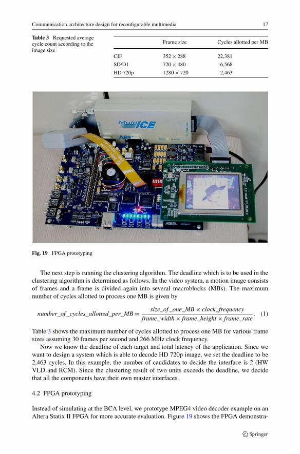
Fig. 19 FPGA prototyping
The next step is running the clustering algorithm. The deadline which is to be used in theclustering algorithm is determined as follows. In the video system, a motion image consistsof frames and a frame is divided again into several macroblocks (MBs). The maximumnumber of cycles allotted to process one MB is given by
number_of _cycles_allotted_per_MB = size_of _one_MB × clock_frequency
frame_width × frame_height × frame_rate. (1)
Table 3 shows the maximum number of cycles allotted to process one MB for various framesizes assuming 30 frames per second and 266 MHz clock frequency.
Now we know the deadline of each target and total latency of the application. Since wewant to design a system which is able to decode HD 720p image, we set the deadline to be2,463 cycles. In this example, the number of candidates to decide the interface is 2 (HWVLD and RCM). Since the clustering result of two units exceeds the deadline, we decidethat all the components have their own master interfaces.
4.2 FPGA prototyping
Instead of simulating at the BCA level, we prototype MPEG4 video decoder example on anAltera Statix II FPGA for more accurate evaluation. Figure 19 shows the FPGA demonstra-
18 G. Lee et al.
Table 4 Implementation details of the architecture
Area Power
LUT number Embedded memory Bits Etc. (DSP number) (mW)
Processor (ARM7TDMI-s) 6,435 – 8 61.56
Master interface 655 – – 3.41
Slave interface 23 – – 0.78
Matrix (3 masters and 4 slaves) 521 – – 3.23
RCM (8 × 8 array PEs) 110,714 95,296 32 1,325.55
HW (VLD) 15,652 1,344 – 121.42
Buffered DRAM controller 2,905 16,384 – 18.93
Fig. 20 Internal structure ofbuffered DRAM controller
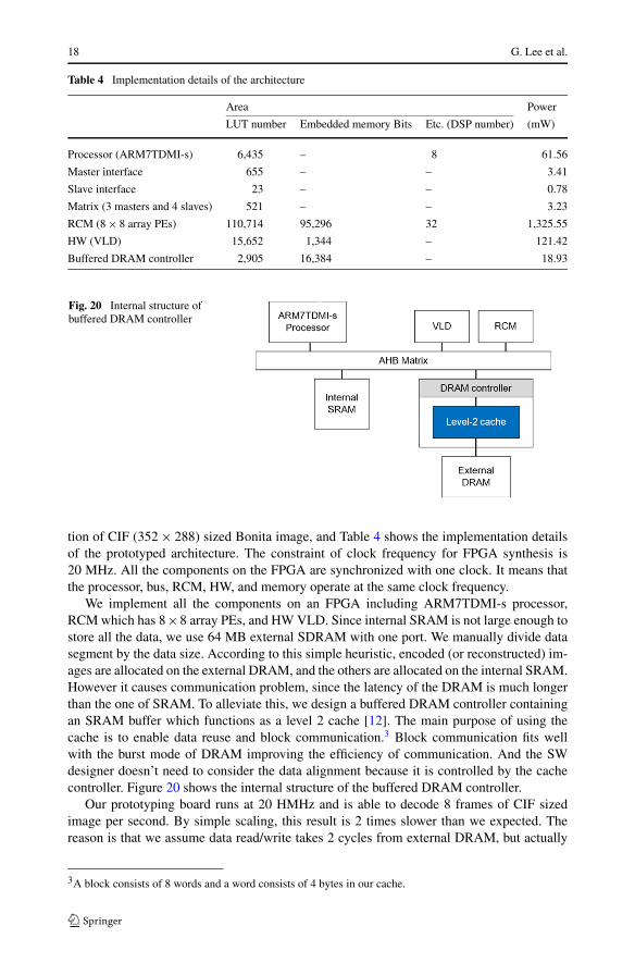
tion of CIF (352 × 288) sized Bonita image, and Table 4 shows the implementation detailsof the prototyped architecture. The constraint of clock frequency for FPGA synthesis is20 MHz. All the components on the FPGA are synchronized with one clock. It means thatthe processor, bus, RCM, HW, and memory operate at the same clock frequency.
We implement all the components on an FPGA including ARM7TDMI-s processor,RCM which has 8×8 array PEs, and HW VLD. Since internal SRAM is not large enough tostore all the data, we use 64 MB external SDRAM with one port. We manually divide datasegment by the data size. According to this simple heuristic, encoded (or reconstructed) im-ages are allocated on the external DRAM, and the others are allocated on the internal SRAM.However it causes communication problem, since the latency of the DRAM is much longerthan the one of SRAM. To alleviate this, we design a buffered DRAM controller containingan SRAM buffer which functions as a level 2 cache [12]. The main purpose of using thecache is to enable data reuse and block communication.3 Block communication fits wellwith the burst mode of DRAM improving the efficiency of communication. And the SWdesigner doesn’t need to consider the data alignment because it is controlled by the cachecontroller. Figure 20 shows the internal structure of the buffered DRAM controller.
Our prototyping board runs at 20 HMHz and is able to decode 8 frames of CIF sizedimage per second. By simple scaling, this result is 2 times slower than we expected. Thereason is that we assume data read/write takes 2 cycles from external DRAM, but actually
3A block consists of 8 words and a word consists of 4 bytes in our cache.
Communication architecture design for reconfigurable multimedia 19
it takes two times longer. It is our future work to modify our DRAM controller for higherefficiency.
5 Conclusions
In this paper, we present an automatic bus matrix synthesis flow. To maximize concurrencyin the communication between HW units, we analyze communication conflicts and performeHW interface selection. The resulting design is simulated with a commercial transaction-level simulator. The proposed synthesis flow is successfully integrated in the MPSoC de-sign environment called SoCDAL with an extended platform with reconfigurable computingmodule.
We demonstrate the effectiveness of the proposed approach with JPEG encoder andH.264 encoder examples, which show 56.91% area and 48.61% power reduction of bus ma-trix with 0.58% delay overhead on average compared to the case of maximum performance.We also test an MPEG4 video decoder through the algorithm, and the result is demonstratedon the FPGA successfully.
As a future research, we are planning to develop an efficient communication architecturedesign for reconfigurable computing module, which includes optimization of HW interfaceas well as SW compiler.
Acknowledgements This work was supported by KOSEF under NRL Program Grant (R0A-2008-000-20126-0) funded by MEST, NIPA under ITRC support program (NIPA-2009-(C1090-0902-0024)) funded byMKE.
References
1. Abdi S, Shin D, Gajski D (2003) Automatic communication refinement for system level design. In: Procof DAC
2. Ahn Y, Han K, Lee G, Song H, Yoo J, Choi K (2008) SoCDAL: System-on-chip design AcceLerator. In:ACM Trans Des Autom Electr Syst
3. Altera Quartus II. http://www.altera.com4. ARM AMBA specifications rev 2.0. http://www.arm.com5. ARM RealView SoCDesigner. http://www.arm.com6. Bauer L, Shafique M, Kramer S, Henkel J (2007) RISPP: rotating instruction set processing platform.
In: Proc of DAC7. Becker J, Vorbach M (2003) Architecture, memory and interface technology integration of an industrial/
academic configurable system-on-chip (CSoC). In: Proc of ISVLSI8. Benini L, Micheli G (2002) Networks on chips: a new SoC paradigm. In: Proc of IEEE comput, Jan
20029. ConvergenSC/Incisive design flow. http://www.coware.com
10. Givargis T, Vahid F (2000) Parameterized system design. In: Proc of CODES11. Han K, Kim J (2004) Quantum-inspired evolutionary algorithms with a new termination criterion, Hε
gate, and two phase scheme. IEEE Trans Evol Comput 812. Hidaka H, Matsuda Y, Asakura M, Fujishima K (1990) The cache DRAM architecture: a DRAM with
an on-chip cache memory. IEEE Trans Microwave13. IBM on-chip CoreConnect bus architecture. http://www.chips.ibm.com14. Keutzer K, Malik S, Newton R, Rabaey J, Sangiovanni-Vincentelli A (2000) System-level design: or-
thogonalization of concerns and platform-based design. IEEE Trans Comput-Aided Des Integr CircuitsSyst
15. Kim Y, Kiemb M, Park C, Jung J, Choi K (2005) Resource sharing and pipelining in coarse-grainedreconfigurable architecture for domain-specific optimization. In: Proc of DATE
16. Kim Y, Park I, Choi K, Paek Y (2006) Power-conscious configuration cache structure and code mappingfor coarse-grained reconfigurable architecture. In: Proc of ISLPED
20 G. Lee et al.
17. Lahiri K, Raghunathan A, Dey S (2004) Design space exploration for optimizing on-chip communicationarchitectures. IEEE Trans Comput-Aided Des Integr Circuits Syst
18. Lee G, Lee S, Ahn Y, Choi K (2007) Automatic bus matrix synthesis based on hardware interface selec-tion for fast communication design space exploration. In: Proc of SAMOS
19. Mei B, Vernalde S, Verkest D, Lauwereins R (2004) Design methodology for a tightly coupledVLIW/reconfigurable matrix architecture: a case study. In: Proc of DATE
20. Multi-layer AHB matrix. http://www.arm.com21. Murali S, De Micheli G (2005) An application specific design methodology for STbus crossbar genera-
tion. In: Proc of DATE22. Nakajima M, Yamamoto T, Ozaki S, Sezaki T, Kanakogi T, Furuzono T, Sakamoto T, Aruga T, Sumita
M, Tsutsumi M, Ueda A, Ichinomiya T (2002) A 400 MHz 32b embedded microprocessor core AM34-1with 4.0 Gb/s cross-bar bus switch for SoC. In: Proc of ISSCC
23. Ogawa O, Noyer S, Chauvet P, Shinohara K, Watanabe Y, Niizuma H, Sasaki T, Takai Y (2003) Apractical approach for bus architecture optimization at transaction level. In: Proc of DATE
24. Open Core Protocol International Partnership (OCP-IP). OCP datasheet. http://www.ocpip.org25. Pasricha S (2002) Transaction level modeling of SoC using SystemC 2.0. 2002. In: Proc of synopsys
user group conference26. Pasricha S, Ben-Romdhane M, Dutt N (2005) Using TLM for exploring bus-base SoC communication
architectures. In: Proc of ASAP27. Pasricha S, Ben-Romdhane M, Dutt N (2006) Constraint-driven bus matrix synthesis for MPSoC. In:
Proc of ASP-DAC28. Rowson J, Sangiovanni-Vincentelli AL (1997) Interface-based design. Proc of DAC29. Singh H, Lee M, Lu G, Kurdahi F, Bagherzadeh N, Filho E (2000) MorphoSys: an integrated reconfig-
urable system for data-parallel and computation-intensive applications. In: IEEE Trans Comput30. STBus communication system: concepts and definitions. In: Reference guide, STMicroelectonics,
Geneva, Switzerland, May 200331. SystemC Intuitive. http://www.systemc.org32. The international technology roadmap for semiconductors, ITRS (2008)33. The SUIF 1.x compiler system. http://suif.stanford.edu/suif/suif1/index.html34. Virtual Socket Interface Alliance Component Interface Standard (OCB 2 1.0) (2000) VSI Alliance35. Yen T, Wolf W (1995) Communication synthesis for distributed embedded systems. In: Proc of ICCAD36. Yoo J, Lee D, Yoo S, Choi K (2007) Communication architecture synthesis of cascaded bus matrix. In:
Proc of ASP-DAC