communication semiconductors c4fm data modem · mux adc 1 thresholds averaging thresholds averaging...
TRANSCRIPT

CML MicrocircuitsCOMMUNICATION SEMICONDUCTORS
CMX7031CMX7041
The Two-Way Radio ProcessorC4FM Data Modem
© 2007 CML Microsystems Plc
D/7031/41_FI3.0/2 April 2007 DATASHEET Advance Information
CMX7031 / CMX7041 – FI 3.0: Baseband Data Processor with Auxiliary System Clocks, ADCs and DACs
Features • C4FM Modem • 4.8 and 9.6 kbits/s Option • Automatic Frame Sync Detection • Raw Mode, Data Pump • Automatic Preamble & Frame Sync Insertion • Auxiliary System Clock Outputs • 2 x Auxiliary ADCs and 4 x Auxiliary DACs • Tx Outputs for Two Point or I & Q Modulation
• 3 x Analogue Inputs (Mic or Discriminator) • Available in 48 or 64-pin, LQFP or VQFN Packages
• C-BUS Serial Interface to Host µController • Low-power (3.0V to 3.6V) Operation
• 2 RF Synthesisers (CMX7031 only) • Flexible Powersave Modes
• Soft Decision Decoding Option for use with with a Vocoder
DatasheetUser
Manual
This document contains:
1 Brief Description
The CMX7031/CMX7041 FI-3.0 is a half-duplex C4FM modem suitable for use in PMR/LMR radio designs in conjunction with a suitable host controller and RF circuits.
The CMX7041 is identical in functionality to the CMX7031 with the exception that the two on-chip RF Synthesisers have been deleted, which enables it to be supplied in a smaller package.
Continued...
CMX7031 / CMX7041The Two-Way Radio Processor
Modulator
RFDiscriminator
Host µCSystem Clock 1
System Clock 2
Optional Vocoder for digital voice
applications
Reference Clock
DAC outputs ADC inputs
3.0V to 3.6V
Built on FirmASIC® technology
GPIO
RF Synthesiser 1RF Synthesiser 2
CMX7031 only

C4FM Data Modem CMX7031/CMX7041
© 2007 CML Microsystems Plc Page 2 D/7031/41_FI3.0/2
The device utilises CML’s proprietary FirmASIC® component technology. On-chip sub-systems are configured by a Function Image™: this is a data file that is uploaded during device initialisation and defines the device's function and feature set. The Function Image™ can be loaded automatically from an external EEPROM or host µController over the built-in C-BUS serial interface. The device's functions and features may be enhanced by subsequent Function Image™ releases, facilitating in-the-field upgrades. This document refers specifically to the features provided by Function Image™ 3.0.
The same device can be loaded with FI-1.x to provide Analogue functionality including simultaneous processing of subaudio and inband signalling and audio band processing (with frequency inversion scrambling, companding and pre- or de-emphasis).
Other features include two Auxiliary ADCs with four selectable inputs and four auxiliary DAC interfaces (with an optional RAMDAC on the first DAC output, to facilitate transmitter power ramping).
The device has flexible powersaving modes and is available in both LQFP and VQFN packages.
Note that text shown in pale grey indicates features that will be supported in future versions of the device.
This Datasheet is the first part of a two-part document comprising Datasheet and User Manual: the User Manual can be obtained by registering your interest in this product with your local CML representative.

C4FM Data Modem CMX7031/CMX7041
© 2007 CML Microsystems Plc Page 3 D/7031/41_FI3.0/2
CONTENTS
Section Page
1 Brief Description.....................................................................................................................1 2 Block Diagram ........................................................................................................................6 3 Signal List................................................................................................................................7 4 External Components ..........................................................................................................10
4.1 Recommended External Components ......................................................................12
5 PCB Layout Guidelines and Power Supply Decoupling...................................................13
6 General Description .............................................................................................................15 6.1 CMX7031/CMX7041 FI 3.0 Features........................................................................15 6.2 System Design ..........................................................................................................15 6.3 Introduction................................................................................................................17
6.3.1 Modulation ...........................................................................................................17 6.3.2 Demodulation ......................................................................................................19 6.3.3 Framing................................................................................................................20 6.3.4 FEC and Coding ..................................................................................................20 6.3.5 Voice Coding .......................................................................................................20 6.3.6 Radio Performance Requirements ......................................................................20
7 Detailed Descriptions...........................................................................................................21 7.1 Xtal Frequency ..........................................................................................................21 7.2 Host Interface ............................................................................................................21
7.2.1 C-BUS Operation.................................................................................................21 7.3 Function Image™ Loading ........................................................................................23
7.3.1 FI Loading from Host Controller ..........................................................................23 7.3.2 FI Loading from EEPROM...................................................................................25
7.4 Device Control ...........................................................................................................26 7.4.1 General Notes .....................................................................................................26 7.4.2 Interrupt Operation ..............................................................................................26 7.4.3 Signal Routing .....................................................................................................27 7.4.4 Modem Control ....................................................................................................27 7.4.5 Tx Mode...............................................................................................................28 7.4.6 Rx Mode ..............................................................................................................29 7.4.7 Other Modem Modes...........................................................................................30 7.4.8 Data Transfer.......................................................................................................30
7.5 Squelch Operation.....................................................................................................31 7.6 GPIO Pin Operation...................................................................................................31 7.7 Auxiliary ADC Operation ...........................................................................................32 7.8 Auxiliary DAC / RAMDAC Operation.........................................................................32 7.9 RF Synthesisers (CMX7031 only) .............................................................................32 7.10 Digital System Clock Generators ..............................................................................36
7.10.1 Main Clock Operation .........................................................................................37 7.10.2 System Clock Operation .....................................................................................37
7.11 Signal Level Optimisation..........................................................................................37 7.11.1 Transmit Path Levels ..........................................................................................37 7.11.2 Receive Path Levels ...........................................................................................37
C4FM Data Modem CMX7031/CMX7041
© 2007 CML Microsystems Plc Page 4 D/7031/41_FI3.0/2
7.12 Tx Spectrum Plots .....................................................................................................38 7.13 C-BUS Register Summary ........................................................................................39
8 Performance Specification ..................................................................................................40 8.1 Electrical Performance ..............................................................................................40
8.1.1 Absolute Maximum Ratings.................................................................................40 8.1.2 Operating Limits ..................................................................................................41 8.1.3 Operating Characteristics....................................................................................42 8.1.4 Parametric Performance......................................................................................48
8.2 C-BUS Timing............................................................................................................49 8.3 Packaging..................................................................................................................50
Table Page
Table 1 Xtal/Clock Frequency Settings for Program Block 3........................................................ 21 Table 2 BOOTEN Pin States ........................................................................................................ 23 Table 3 Modem Mode Selection ................................................................................................... 27 Table 4 Modem Control Selection.................................................................................................. 28 Table 5 C-BUS Data Registers ..................................................................................................... 31 Table 6 C-BUS Registers.............................................................................................................. 39
Figure Page
Figure 1 CMX7031 / 7041 Block Diagram ....................................................................................... 6 Figure 2 CMX7031 Recommended External Components ........................................................... 10 Figure 3 CMX7041 Recommended External Components ........................................................... 11 Figure 4 CMX7031 Power Supply and De-coupling ...................................................................... 13 Figure 5 CMX7041 Power Supply and De-coupling ...................................................................... 14 Figure 6 Digital Voice Rx and Tx Blocks........................................................................................ 16 Figure 7 C4FM PRBS Waveform (eye diagram) ........................................................................... 18 Figure 8 Modulation Performance ................................................................................................. 19 Figure 9 C-BUS Transactions ........................................................................................................ 22 Figure 10 FI Loading from Host ..................................................................................................... 24 Figure 11 FI Loading from EEPROM............................................................................................. 25 Figure 12 Tx Data Flow.................................................................................................................. 29 Figure 13 Rx Data Flow ................................................................................................................. 30 Figure 14 Example RF Synthesiser Components for a 512MHz Receiver .................................. 33 Figure 15 Single RF Channel Block Diagram............................................................................... 34 Figure 16 Digital Clock Generation Schemes................................................................................ 36 Figure 17 Tx Modulation Spectra, 9600bps, 2-point modulation mode......................................... 38 Figure 18 C-BUS Timing................................................................................................................ 49 Figure 19 Mechanical outline for 64-pad VQFN (Q1) .................................................................... 50 Figure 20 Mechanical outline for 64-pin LQFP (L9)....................................................................... 50 Figure 21 Mechanical Outline of 48-pin VQFN (Q3)...................................................................... 51 Figure 22 Mechanical Outline of 48-pin LQFP (L4) ....................................................................... 51

C4FM Data Modem CMX7031/CMX7041
© 2007 CML Microsystems Plc Page 5 D/7031/41_FI3.0/2
Information in this data sheet should not be relied upon for final product design. It is always recommended that you check for the latest product datasheet version from the CML website: [www.cmlmicro.com]. Note: This product is in development: Changes and additions will be made to this
specification. Items marked TBD or left blank will be included in later issues.

C4FM Data Modem CMX7031/CMX7041
© 2007 CML Microsystems Plc Page 6 D/7031/41_FI3.0/2
2 Block Diagram
ALT IN
DISC
GPIO 1/Tx ENABLE
GPIO 2/Rx ENABLE
GPIO A
GPIO B
Data Demodulator
Transmit FunctionsMOD1
AUDIO OUT
MOD2
MIC IN
ADC I/P 1
ADC I/P 2
ADC I/P 3
ADC I/P 4
DAC 1
EPSCLK
BO
OT
EN
1
BO
OT
EN
2
EPCSN
Output 2
Output 1
SYS CLK 1
SYS CLK 2
DAC 2
DAC 3
DAC 4
AV
DD
VB
IAS
AV
SS
XT
AL/
CLK
XT
ALN
EPSO
EPSI
Auxiliary Multiplexed ADCs
Auxiliary DACs
Auxiliary System Clocks
System Control
Internal Signal
TxModulato
rMode
Sinc-1
Filter
Raised CosineFilter
4-level Modulator
TxData
Buffer
Data Modulator
AnalogueRouting
VBIAS
VBIAS
VBIAS
SincFilter
Rx Eye
AFSD
DemodulatorRx
DataBuffer
GPIO
FI Configured I/O
DAC 1
DAC 2
DAC 3
DAC 4
Ramp Profile RAM
MUX
ADC 1Thresholds
Averaging
Thresholds
Averaging
System Clock 1
System Clock 2
C-BUSInterface
IRQN
REPLY DATA
CSN
CMD DATA
SERIAL CLK
Power Control
Registers
EEPROMInterface
Bias
DV
DD
VD
EC
DV
SS
BiasCrystal
Oscillator
Boot Control
Main Clock PLL
Auxiliary Functions
Receive Functions Tone Generator
ADC 2
Synthesiser 1
RF1-
CP1OUT
ISET1
Synthesiser 1
RF2-
CP2OUT
ISET2
RFVDD
CPVDD
RFVSS
RFCLKRF Synthesisers
(CMX7031 only)
GPIO(CMX7041 only)
RF1+
RF2+
MIC FB
ALT FB
DISC FB
Raw Data
Test Mode
Raw Data
Figure 1 CMX7031 / 7041 Block Diagram
C4FM Data Modem CMX7031/CMX7041
© 2007 CML Microsystems Plc Page 7 D/7031/41_FI3.0/2
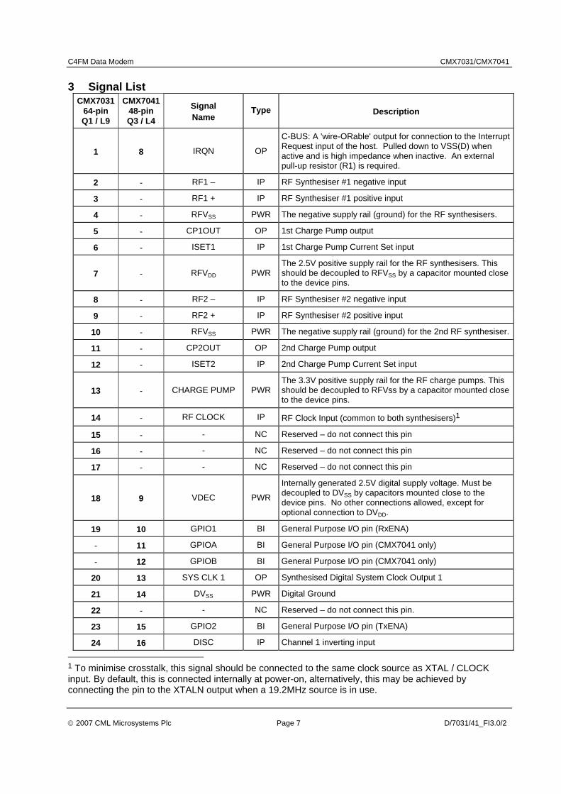
3 Signal List CMX7031
64-pin Q1 / L9
CMX7041 48-pin Q3 / L4
Signal Name
Type Description
1 8 IRQN OP
C-BUS: A 'wire-ORable' output for connection to the Interrupt Request input of the host. Pulled down to VSS(D) when active and is high impedance when inactive. An external pull-up resistor (R1) is required.
2 - RF1 – IP RF Synthesiser #1 negative input
3 - RF1 + IP RF Synthesiser #1 positive input
4 - RFVSS PWR The negative supply rail (ground) for the RF synthesisers.
5 - CP1OUT OP 1st Charge Pump output
6 - ISET1 IP 1st Charge Pump Current Set input
7 - RFVDD PWR The 2.5V positive supply rail for the RF synthesisers. This should be decoupled to RFVSS by a capacitor mounted close to the device pins.
8 - RF2 – IP RF Synthesiser #2 negative input
9 - RF2 + IP RF Synthesiser #2 positive input
10 - RFVSS PWR The negative supply rail (ground) for the 2nd RF synthesiser.
11 - CP2OUT OP 2nd Charge Pump output
12 - ISET2 IP 2nd Charge Pump Current Set input
13 - CHARGE PUMP PWR The 3.3V positive supply rail for the RF charge pumps. This should be decoupled to RFVss by a capacitor mounted close to the device pins.
14 - RF CLOCK IP RF Clock Input (common to both synthesisers)1
15 - - NC Reserved – do not connect this pin
16 - - NC Reserved – do not connect this pin
17 - - NC Reserved – do not connect this pin
18 9 VDEC PWR
Internally generated 2.5V digital supply voltage. Must be decoupled to DVSS by capacitors mounted close to the device pins. No other connections allowed, except for optional connection to DVDD.
19 10 GPIO1 BI General Purpose I/O pin (RxENA)
- 11 GPIOA BI General Purpose I/O pin (CMX7041 only)
- 12 GPIOB BI General Purpose I/O pin (CMX7041 only)
20 13 SYS CLK 1 OP Synthesised Digital System Clock Output 1
21 14 DVSS PWR Digital Ground
22 - - NC Reserved – do not connect this pin.
23 15 GPIO2 BI General Purpose I/O pin (TxENA)
24 16 DISC IP Channel 1 inverting input
1 To minimise crosstalk, this signal should be connected to the same clock source as XTAL / CLOCK input. By default, this is connected internally at power-on, alternatively, this may be achieved by connecting the pin to the XTALN output when a 19.2MHz source is in use.

C4FM Data Modem CMX7031/CMX7041
© 2007 CML Microsystems Plc Page 8 D/7031/41_FI3.0/2
CMX7031 64-pin Q1 / L9
CMX7041 48-pin Q3 / L4
Signal Name
Type Description
25 17 DISCFB OP Channel 1 input amplifier feedback
26 18 ALT IP Channel 2 inverting input
27 19 ALTFB OP Channel 2 input amplifier feedback
28 20 MICFB OP Channel 3 input amplifier feedback
29 21 MICIN IP Channel 3 inverting input
30 22 AVSS PWR Analog Ground
31 23 MOD1 OP Modulator 1 output
32 24 MOD2 OP Modulator 2 output
33 25 VBIAS OP
Internally generated bias voltage of about AVDD/2, except when the device is in ‘Powersave’ mode when VBIAS will discharge to AVSS. Must be decoupled to AVSS by a capacitor mounted close to the device pins. No other connections allowed.
34 26 AUDIO OUT OP Reserved for future use2
35 27 AUXADC1 IP Auxiliary ADC input 1
36 28 AUXADC2 IP Auxiliary ADC input 2
37 29 AUXADC3 IP Auxiliary ADC input 3
38 30 AUXADC4 IP Auxiliary ADC input 4
39 31 AVDD PWR
Analog +3.3V supply rail. Levels and thresholds within the device are proportional to this voltage. This pin should be decoupled to AVSS by capacitors mounted close to the device pins.
40 32 AUXDAC1 OP Auxiliary DAC output 1 / RAMDAC
41 33 AUXDAC2 OP Auxiliary DAC output 2
42 34 AVSS PWR Analog Ground
43 35 AUXDAC3 OP Auxiliary DAC output 3
44 36 AUXDAC4 OP Auxiliary DAC output 4
- 37 DVSS PWR Digital Ground
45 38 VDEC PWR
Internally generated 2.5V supply voltage. Must be decoupled to DVSS by capacitors mounted close to the device pins. No other connections allowed, except for the optional connection to RFVDD.
46 39 XTAL / CLOCK IP Input from the external clock source or Xtal
47 40 XTALN OP The output of the on-chip Xtal oscillator inverter. NC if external Clock used.
48 41 DVDD PWR Digital +3.3V supply rail. This pin should be decoupled to DVSS by capacitors mounted close to the device pins.
49 42 COMMAND DATA IP C-BUS: Serial data input from the µC. 2 The AUDIO OUT pin is not currently used in this FI, however it has been included here for compatibility with FI 1.x

C4FM Data Modem CMX7031/CMX7041
© 2007 CML Microsystems Plc Page 9 D/7031/41_FI3.0/2
CMX7031 64-pin Q1 / L9
CMX7041 48-pin Q3 / L4
Signal Name
Type Description
50 43 REPLY DATA TS OP C-BUS: A 3-state C-BUS serial data output to the µC. This output is high impedance when not sending data to the µC.
51 44 - NC Reserved – do not connect this pin.
52 45 DVSS PWR Digital Ground.
53 - - NC Reserved – do not connect this pin.
54 46 SERIAL CLOCK IP C-BUS: The C-BUS serial clock input from the µC.
55 47 SYS CLK 2 OP Synthesised Digital System Clock Output 2.
56 48 CSN IP C-BUS: The C-BUS chip select input from the µC
57 - - NC Reserved – do not connect this pin.
58 1 EPSI OP EEPROM Serial Interface: SPI bus Output.
59 2 EPSCLK OP EEPROM Serial Interface: SPI bus Clock.
60 3 EPSO IP+PD EEPROM Serial Interface: SPI bus Input.
61 4 EPSCSN OP EEPROM Serial Interface: SPI bus Chip Select.
62 5 BOOTEN1 IP+PD Used in conjunction with BOOTEN2 to determine the operation of the bootstrap program.
63 6 BOOTEN2 IP+PD Used in conjunction with BOOTEN1 to determine the operation of the bootstrap program.
64 7 DVSS PWR Digital Ground
Notes: IP = Input (+ PU/PD = internal pullup / pulldown resistor) OP = Output BI = Bidirectional TS OP = 3-state Output PWR = Power Connection NC = No Connection - should NOT be connected to any signal.

C4FM Data Modem CMX7031/CMX7041
© 2007 CML Microsystems Plc Page 10 D/7031/41_FI3.0/2
4 External Components
Figure 2 CMX7031 Recommended External Components

C4FM Data Modem CMX7031/CMX7041
© 2007 CML Microsystems Plc Page 11 D/7031/41_FI3.0/2
AuxADC
AuxDAC
CBUS
18C5
C7 C6
AUX DAC 2
AUX DAC 1
VD
EC
VDEC AUX ADC 2
AUX ADC 4
AVDD
DVDD
DVDD
AVDD
XTA
L/C
LKAUX ADC 1
AUX ADC 3IRQN
XTA
LN
DV S
S
DVSS
AUDIO OUT Audio
AVSS AVSS
DV S
SDVSS
DVSS
AVSS AVSS
DV D
D
SYS
CLK
2
VBIAS
CO
MM
AND
DAT
A
SER
IAL
CLO
CK
RE
PLY
DAT
A
CS
N
n/c
EPSI
EPSCLK
EPSO
EPSCSN
BOOTEN1
BOOTEN2
C1
X1C2
C3
C4
R2
R1
+
CMX7041L4
1
2
3
4
5
6
7
8
9
10
11
1213 14 15 16 17
C17
C15C13C11
C18 C19
MO
D 1
MO
D 2
AVS
S
MIC
DIS
C
GPIOB
GPIOA
GPIO1
SYS
CLK
1
MIC
FB
ALT
FB
GP
IO2
ALT
DV
SS
DIS
C F
B
C16C14
C12
C9
C8
MOD 2
MIC
DISC
ALT
MOD 1
AVSS
AVSS
DVSS
AVSSAVDD
AVSS AVSS AVSS
R3
R4R10R8
R9R7R5
R6
+C20 C21 C22
DVDD
DVSS DVSS DVSS
+
C24 C23
DVSS DVSS
+
AUXDAC 3
AUX DAC 4
Figure 3 CMX7041 Recommended External Components

C4FM Data Modem CMX7031/CMX7041
© 2007 CML Microsystems Plc Page 12 D/7031/41_FI3.0/2
4.1 Recommended External Components R1 100kΩ C1 18pF C11 See note 5 C21 10nF R2 100kΩ C2 18pF C12 100pF C22 10nF R3 100kΩ C3 10nF C13 See note 5 C23 10µF R4 100kΩ C4 10µF C14 100pF C24 10nF R5 See note 2 C5 1nF C15 See note 5 C25 10nF R6 100kΩ C6 100pF C16 200pF C26 10µF R7 See note 3 C7 100nF C17 10µF R8 100kΩ C8 100pF C18 10nF X1 6.144MHz R9 See note 4 C9 100pF C19 10nF See note 1
R10 100kΩ C10 not used C20 10µF
Resistors ±5%, capacitors and inductors ±20% unless otherwise stated. Notes: 1. X1 can be a crystal or an external clock generator; this will depend on the application. The tracks
between the crystal and the device pins should be as short as possible to achieve maximum stability and best start up performance. By default, a 6.144MHz crystal is assumed, other values could be used if the various internal clock dividers are set to appropriate values.
2. R5 should be selected to provide the desired dc gain (assuming C11 is not present) of the discriminator input, as follows:
GAINDisc = 100kΩ / R5 The gain should be such that the resultant output at the DISCFB pin is within the discriminator input signal range specified in 7.11.2.
3. R7 should be selected to provide the desired dc gain (assuming C13 is not present) of the alternative input as follows:
GAINAlt = 100kΩ / R7 The gain should be such that the resultant output at the ALTFB pin is within the alternative input signal range specified in 7.11.
4. R9 should be selected to provide the desired dc gain (assuming C15 is not present) of the microphone input as follows:
GAINMic = 100kΩ / R9 The gain should be such that the resultant output at the MICFB pin is within the microphone input signal range specified in 7.11.1. For optimum performance with low signal microphones, an additional external gain stage may be required.
5. C11, C13 and C15 should be selected to maintain the lower frequency roll-off of the microphone, alternative and discriminator inputs as follows:
C11 ≥ 1.0µF × GAINDisc C13 ≥ 1.0µF × GAINAlt C15 ≥ 30nF × GAINMic
6. ALT and ALTFB connections allow the user to have a second discriminator or microphone input. Component connections and values are as for the respective DISC and MIC networks. If this input is not required, the ALT pin should be connected to AVss.

C4FM Data Modem CMX7031/CMX7041
© 2007 CML Microsystems Plc Page 13 D/7031/41_FI3.0/2
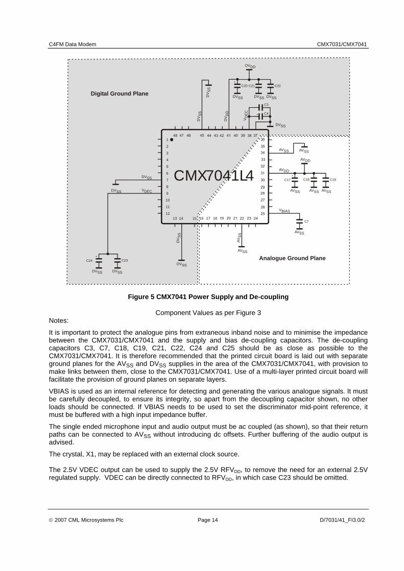
5 PCB Layout Guidelines and Power Supply Decoupling
Figure 4 CMX7031 Power Supply and De-coupling
Component Values as per Figure 2
C4FM Data Modem CMX7031/CMX7041
© 2007 CML Microsystems Plc Page 14 D/7031/41_FI3.0/2
18C7
V DEC
VDEC
AVDD
DV S
S
DVSS
AVSS AVSS
DV S
S
DVSS
DVSS
AVSS
DV
DD
VBIAS
C3
C4+
CMX7041L4
1
2
3
4
5
6
7
8
9
10
11
1213 14 15 16 17
C17 C18 C19
AVSS
DV S
S
AVSS
DVSS
AVDD
AVSS AVSS AVSS
+
C20 C21 C22
DVDD
DVSS DVSS DVSS
+
C24
Digital Ground Plane
Analogue Ground PlaneC23
DVSS DVSS
+
Figure 5 CMX7041 Power Supply and De-coupling
Component Values as per Figure 3 Notes:
It is important to protect the analogue pins from extraneous inband noise and to minimise the impedance between the CMX7031/CMX7041 and the supply and bias de-coupling capacitors. The de-coupling capacitors C3, C7, C18, C19, C21, C22, C24 and C25 should be as close as possible to the CMX7031/CMX7041. It is therefore recommended that the printed circuit board is laid out with separate ground planes for the AVSS and DVSS supplies in the area of the CMX7031/CMX7041, with provision to make links between them, close to the CMX7031/CMX7041. Use of a multi-layer printed circuit board will facilitate the provision of ground planes on separate layers.
VBIAS is used as an internal reference for detecting and generating the various analogue signals. It must be carefully decoupled, to ensure its integrity, so apart from the decoupling capacitor shown, no other loads should be connected. If VBIAS needs to be used to set the discriminator mid-point reference, it must be buffered with a high input impedance buffer.
The single ended microphone input and audio output must be ac coupled (as shown), so that their return paths can be connected to AVSS without introducing dc offsets. Further buffering of the audio output is advised.
The crystal, X1, may be replaced with an external clock source. The 2.5V VDEC output can be used to supply the 2.5V RFVDD, to remove the need for an external 2.5V regulated supply. VDEC can be directly connected to RFVDD, in which case C23 should be omitted.

C4FM Data Modem CMX7031/CMX7041
© 2007 CML Microsystems Plc Page 15 D/7031/41_FI3.0/2
6 General Description 6.1 CMX7031/CMX7041 FI 3.0 Features The CMX7031 / CMX7041 FI 3.0 is intended for use in half duplex digital two way mobile radio equipment using C4FM modulation at 4800 or 9600 bps. The ability to re-load the device with FI 1.x allows the same platform to offer backwards compatibility with existing analogue radio systems. A flexible power control facility allows the device to be placed in its optimum powersave mode when not actively processing signals.
The device includes a crystal clock generator, with buffered output, to provide a common system clock if required.
A block diagram of the device is shown in Figure 1.
The signal processing blocks can be routed from any of the three audio / discriminator input pins.
Tx Functions: o 72bit Tx data buffer o Automatic Preamble & Frame Sync insertion simplifies host control o C4FM baseband modulator o Raised Cosine (RC) and Inverse Sinc filter o RAMDAC operation o TxENA hardware signal o Two-point or I & Q modulation outputs
Rx Functions:
o Discriminator input with input amplifier and programmable gain adjustment o 72bit Rx data buffer o Automatic Frame Sync detection simplifies host control o Selectable squelch source o Modulation (Sinc) filtering (selectable) o C4FM baseband demodulator o Hard or Soft data options o RxENA hardware control signal
Auxiliary Functions:
o 2 programmable system clock outputs o 2 auxiliary ADCs with four selectable input paths o 4 auxiliary DACs, one with built-in programmable RAMDAC o 2 RF synthesiser / PLLs (CMX7031 only)
Interface:
o Optimised C-BUS (4 wire high speed synchronous serial command / data bus) interface to host for control and data transfer
o Open drain IRQ to host o Two GPIO pins (CMX7041 only) o EEPROM boot mode o C-BUS (host) boot mode
6.2 System Design Figure 6 shows a possible implementation of the CMX7031 / 7041 combined with a CMX618, a Host µController and suitable RF sections to provide a digital PMR radio. The bold lines show the active signal paths in Rx and Tx respectively.

C4FM Data Modem CMX7031/CMX7041
© 2007 CML Microsystems Plc Page 16 D/7031/41_FI3.0/2
Figure 6 Digital Voice Rx and Tx Blocks
The paralleling of the Mic and Spkr connections is required if the CMX7031/CMX7041 is to provide full analogue PMR functionality, as provided in FI 1.x. The Audio Codec and Voice Codec functionality can also be provided by a suitable Vocoder product such as the CMX618 RALCWI Vocoder.
The AuxADC can be used to detect the Squelch signal from the RF section, while still retaining a significant degree of powersaving within the CMX7031/CMX7041 and avoiding the need to wake the host up unnecessarily. The use of the programmable thresholds allows for user selection of squelch threshold settings programmed by the host.
Before any data is transmitted over the air, the initial data needs to be loaded from the host into the C-BUS TxData registers. The CMX7031/CMX7041 can be transmitting data from the modem while at the same time receiving the next data block from the host. In Rx, the host needs to understand that there will be a delay from receiving the data over the air to the data arriving at its input while the CMX7031/CMX7041 filters and demodulates the incoming signal before presenting it to the output buffer. These buffering and coding processes will add delays to the overall data stream, which will add to the delays in transferring the data between the CMX7031/CMX7041 and the host and subsequently from the host to the Voice Codec.
In order to offer the best performance, the demodulator can be set to output soft-decision data compatible with the CMX618 Vocoder during reception of voice payload data. This mode increases the Rx data rates over the host C-BUS by a factor of 4. The soft decision data is transferred as 4-bits, log-likelihood ratio encoded.
Host
Host
CMX7031 / CMX7041
CMX7031 / CMX7041
RF Section
Vocoder
Disc
TXmod1TXmod2PAramp
spi port
cbus clkcbus dataincbus csn0cbus dataout
csn1
Mic
Spkr
modemcoding
RF Section
Vocoder
Disc
TXmod1TXmod2PAramp
spi port
cbus clkcbus dataincbus csn0cbus dataout
csn1
Mic
Spkr
modemcoding
Audio Codec
Audio Codec
SquelchRx_ena
Tx_ena
SquelchRx_ena
Tx_ena
protocol
protocol

C4FM Data Modem CMX7031/CMX7041
© 2007 CML Microsystems Plc Page 17 D/7031/41_FI3.0/2
6.3 Introduction This modem can run at either 4800bps or 9600bps. In the 9600bps mode, this will occupy a 12.5kHz bandwidth RF channel. It has been designed such that, when combined with suitable RF, Host controller and Vocoder hardware and appropriate software, it meets the requirements of the TIA/EIA P25 Common Air Interface standards (as listed in the text).
6.3.1 Modulation The C4FM scheme running at 9600bps (4800 symbols/s) is normally used with a Raised Cosine (RC) filter so as to fit inside a 12.5kHz channel bandwidth. Details of the modulation are as follows:
4 LevelEncoder
RC FilterShaping Filter(inverse sinc)
Input(Bits)
Output(C4FM)
Inputs to the 4-level encoder are converted to symbol values as follows:
Bits Symbol Deviation 01 +3 +1.8kHz 00 +1 +0.6kHz 10 -1 -0.6kHz 11 -3 -1.8kHz
The symbol input to the Raised Cosine filter is a series of digital “impulses” as described in TIA -102.BAAA paragraph 9.3.
The Raised Cosine filter has alpha = 0.2 and has a linear phase and frequency response as follows:
=)( fH
⎪⎪⎪
⎭
⎪⎪⎪
⎬
⎫
⎪⎪⎪
⎩
⎪⎪⎪
⎨
⎧
>
<<⎟⎠⎞
⎜⎝⎛ •••+
<
Hzf
Hzff
Hzf
2880for 0
28801920for 1920
2cos5.05.0
1920for 1
π
The shaping filter has a linear phase frequency response as follows:
=)( fH
⎪⎪⎪⎪⎪⎪
⎭
⎪⎪⎪⎪⎪⎪
⎬
⎫
⎪⎪⎪⎪⎪⎪
⎩
⎪⎪⎪⎪⎪⎪
⎨
⎧
>
≤≤⎟⎠⎞
⎜⎝⎛ ⋅
⋅
<⎟⎠⎞
⎜⎝⎛ ⋅
⋅
Hzf
Hzff
f
Hzff
f
3500for 0
35002880for
4800sin
4800
2880for
4800sin
4800
π
π
π
π

C4FM Data Modem CMX7031/CMX7041
© 2007 CML Microsystems Plc Page 18 D/7031/41_FI3.0/2
The roll-off of the combined filters has been optimised to achieve good adjacent channel power (ACIPR) at the same time as the desired pass-band characteristics (see section 7.12).
The 4800bps (2400 symbols/s) mode is essentially the same, but with the timings modified by a factor of two.
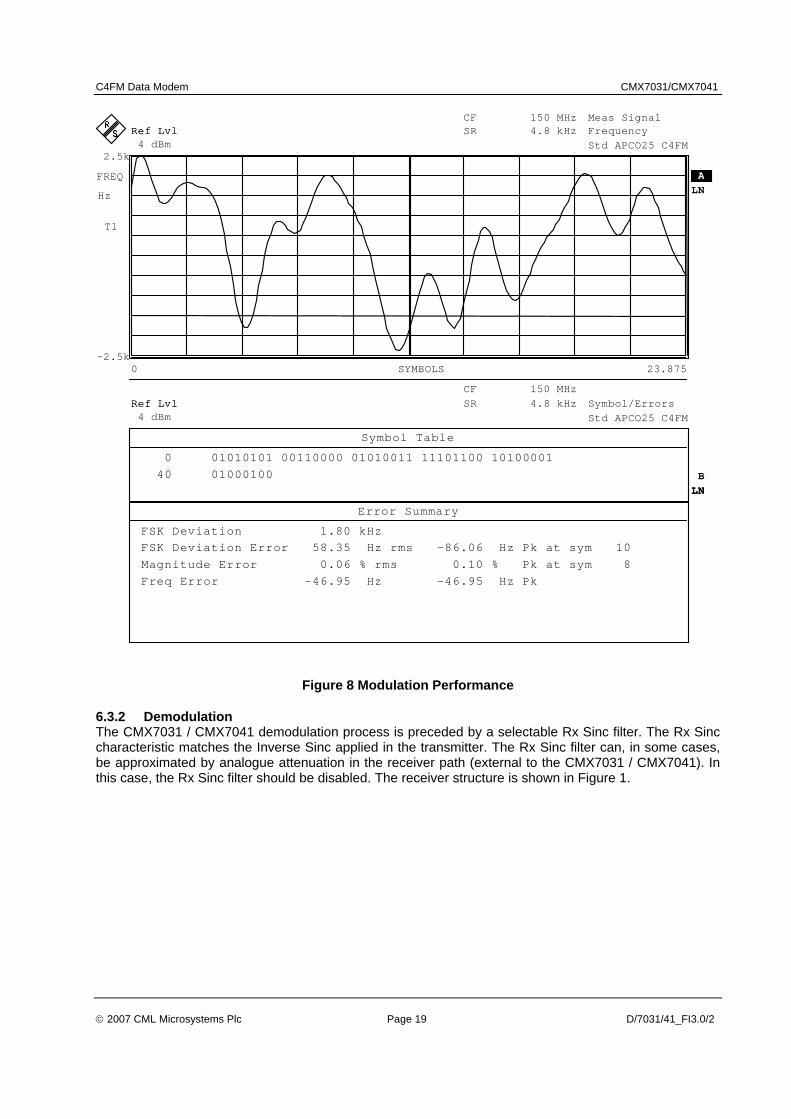
Figure 7 and Figure 8 show the transmitted PRBS waveform as shown on a spectrum analyser, having been modulated using a suitable RF transmitter (2-point modulation mode).
R e f
L v l 4 d B m 4 d B m R e f
L v l 4 d B m 4 d B m
CF 150 M H z
SR
4.8 k H z
M e a s S i g n al
E y e [ I ]
S t d A P C O 2 5 C4FM
R E A L
T 1
A LNLN
0 4SYMBOLS- 2 5 0 m
2 5 0 m
T S 1 T S 2
Figure 7 C4FM PRBS Waveform (eye diagram)
C4FM Data Modem CMX7031/CMX7041
© 2007 CML Microsystems Plc Page 19 D/7031/41_FI3.0/2
R e f L v l
4 d B m R e f
L v l 4 d B m R e f
L v l 4 d B m R e f
L v l 4 d B m
CF 150 M H z
SR
4.8 k H z SR
4.8
k H z
S y m b o l / E r rorsS t d
A P C O 2 5 C4FMS t d A P C O 2 5 C4FM
LNLN B
H z
R e f L v l
4 d B m R e f
L v l 4 d B m R e f
L v l 4 d B m R e f
L v l 4 d B m
CF 150 M H z
SR
4.8 k H z SR
4.8
k H z
M e a s S i g n al
F r e q u e n c y F r e q u e n c y S t d
A P C O 2 5 C4FMS t d A P C O 2 5 C4FM
F R E Q
T 1
A LNLN
0 2 3.875SYMBOLS- 2 . 5 k
2 . 5 k
Symbol Table 0 0 1 010 1 0 1 0 0 1 1 0 000 01010011 11101100 10100001 4 0 0 1 000 1 0 0
Error SummaryF S K D e v i a t i on 1.80 kHz F S K D e v i a t i on E r r o r 5 8.35 Hz rms -86.06 Hz Pk at s y m 1 0 M a g n i t u d e E rro r 0.06 % rms 0.10 % Pk at s y m 8 F r e q E r r o r - 4 6.95 Hz -46.95 Hz Pk
Figure 8 Modulation Performance
6.3.2 Demodulation The CMX7031 / CMX7041 demodulation process is preceded by a selectable Rx Sinc filter. The Rx Sinc characteristic matches the Inverse Sinc applied in the transmitter. The Rx Sinc filter can, in some cases, be approximated by analogue attenuation in the receiver path (external to the CMX7031 / CMX7041). In this case, the Rx Sinc filter should be disabled. The receiver structure is shown in Figure 1.

C4FM Data Modem CMX7031/CMX7041
© 2007 CML Microsystems Plc Page 20 D/7031/41_FI3.0/2
6.3.3 Framing The CMX7031/CMX7041 FI-3 uses a 72-bit preamble and a 24-bit Frame Sync. Both the Preamble and Frame Sync’s are user-programmable, see User Manual sections 10.1.28 bit 1 and 10.2.1.
6.3.4 FEC and Coding The CMX7031/CMX7041 does not implement any FEC, coding or interleaving. These protocol dependant functions should be performed by the host µController.
6.3.5 Voice Coding The CML CMX618 and CMX608 are suitable devices for this application.
In both cases, the Voice Decoder (in Rx mode) may require 4-bit log-likelihood encoded soft coded data from the modem. This increases the C-BUS data rate by a factor of 4 in the Rx state (each bit received over the RF channel is encoded into a 4-bit value over the C-BUS).
6.3.6 Radio Performance Requirements It should be noted that the CMX7031/CMX7041 demodulator is designed to process a demodulated C4FM signal from a limiter / discriminator source. For optimum performance the demodulated signal should not be significantly degraded by filters that are excessively narrow and / or cause significant group delay distortion.

C4FM Data Modem CMX7031/CMX7041
© 2007 CML Microsystems Plc Page 21 D/7031/41_FI3.0/2
7 Detailed Descriptions 7.1 Xtal Frequency The CMX7031/CMX7041 is designed to work with a Xtal or external frequency source of 6.144MHz. If this default configuration is not used, then Program Register Block 3 must be loaded with the correct values to ensure that the device will work to specification with the user selected clock frequency. A table of common values can be found in Table 1. Note the maximum Xtal frequency is 12.288MHz, although an external clock source of up to 24MHz can be used. The register values in Table 1 are shown in hex, the default settings are shown in bold, and the settings which do not give an exact setting (but are within acceptable limits) are in italics. The new P3.2-3 settings take effect following the write to P3.3 (the settings in P3.4-7 are implemented on a change to Rx or Tx mode).
Table 1 Xtal/Clock Frequency Settings for Program Block 3
Program Register External frequency source (MHz)
3.579 6.144 9.0592 12.0 12.8 16.368 16.8 19.2 P3.2
GP Timer $017 $018 $018 $019 $019 $018 $019 $018
P3.3 Idle
VCO output and AUX clk divide $085 $088 $10F $10F $110 $095 $115 $099
P3.4 Ref clk divide $043 $040 $0C6 $07D $0C8 $155 $15E $0C8
P3.5 PLL clk divide $398 $200 $370 $200 $300 $400 $400 $200
P3.6 VCO output and AUX clk divide $140 $140 $140 $140 $140 $140 $140 $140
P3.7
Rx
or T
x
Internal ADC / DAC clk divide $008 $008 $008 $008 $008 $008 $008 $008
7.2 Host Interface A serial data interface (C-BUS) is used for command, status and data transfers between the CMX7031/CMX7041 and the host µC; this interface is compatible with microwire, SPI. Interrupt signals notify the host µC when a change in status has occurred and the µC should read the status register across the C-BUS and respond accordingly. Interrupts only occur if the appropriate mask bit has been set. See section 7.4.2.
7.2.1 C-BUS Operation This block provides for the transfer of data and control or status information between the CMX7031/CMX7041’s internal registers and the host µC over the C-BUS serial interface. Each transaction consists of a single Address byte sent from the µC which may be followed by one or more data byte(s) sent from the µC to be written into one of the CMX7031/CMX7041’s Write Only Registers, or one or more data byte(s) read out from one of the CMX7031/CMX7041’s Read Only Registers, as shown in Figure 9.
Data sent from the µC on the Command Data line is clocked into the CMX7031/CMX7041 on the rising edge of the Serial Clock input. Reply Data sent from the CMX7031/CMX7041 to the µC is valid when the Serial Clock is high. The CSN line must be held low during a data transfer and kept high between transfers. The C-BUS interface is compatible with most common µC serial interfaces and may also be easily implemented with general purpose µC I/O pins controlled by a simple software routine.
The number of data bytes following an Address byte is dependent on the value of the Address byte. The most significant bit of the address or data are sent first. For detailed timings see section 8.2. Note that, due to internal timing constraints, there may be a delay of up to 250µs between the end of a C-BUS write operation and the device reading the data from its internal register.

C4FM Data Modem CMX7031/CMX7041
© 2007 CML Microsystems Plc Page 22 D/7031/41_FI3.0/2
C-BUS Write:
See Note 1 See Note 2 CSN Serial_Clock CMD_DATA 7 6 5 4 3 2 1 0 7 6 … 0 7 … 0 MSB LSB MSB LSB MSB LSB
Address / Command byte Upper 8 bits Lower 8 bits
REPLY_DATA
High Z state C-BUS Read:
See Note 2 CSN Serial_Clock CMD_DATA 7 6 5 4 3 2 1 0 MSB LSB
Address byte Upper 8 bits Lower 8 bits
REPLY_DATA 7 6 … 0 7 … 0
High Z state MSB LSB MSB LSB
Data value unimportant
Repeated cycles
Either logic level valid (and may change)
Either logic level valid (but must not change from low to high)
Figure 9 C-BUS Transactions Notes:
1. For Command byte transfers only the first 8 bits are transferred ($01 = Reset). 2. For single byte data transfers only the first 8 bits of the data are transferred. 3. The CMD_DATA and REPLY_DATA lines are never active at the same time. The Address byte
determines the data direction for each C-BUS transfer. 4. The Serial_Clock input can be high or low at the start and end of each C-BUS transaction. 5. The gaps shown between each byte on the CMD_DATA and REPLY_DATA lines in the above
diagram are optional, the host may insert gaps or concatenate the data as required.
C4FM Data Modem CMX7031/CMX7041
© 2007 CML Microsystems Plc Page 23 D/7031/41_FI3.0/2
7.3 Function Image™ Loading The Function Image™ (FI), which defines the operational capabilities of the device, may be obtained from the CML Technical Portal, following registration. This is in the form of a 'C' header file which can be included into the host controller software or programmed into an external EEPROM. The maximum possible size of Function ImageTM is 46kbytes, although a typical FI will be less than this. Note that the BOOTEN pins are only read at power-on or following a C-BUS General Reset and must remain stable throughout the FI loading process. Once the FI load has completed, the BOOTEN pins are ignored by the CMX7031 until the next power-up or C-BUS General Reset. The BOOTEN pins are both fitted with internal 100k (approx.) pull down resistors.
For C-BUS load operation, both pins should be pulled high by connecting them to DVDD either directly or via a 4k7 resistor (see Table 2).
For EEPROM load, only BOOTEN1 needs to be pulled high in a similar manner, however, if it is required to program the EEPROM in-situ from the host, either a jumper to DVDD or a link to a host I/O pin should be provided to pull BOOTEN2 high when required (see Table 2).
Once the FI has been loaded, the CMX7031/CMX7041 performs these actions:
(1) the product identification code ($7031 or $7041) is reported in C-BUS register $C5 (2) the FI version code is reported in C-BUS register $C9 (3) the two 32-bit FI checksums are reported in C-BUS register pairs $A9, $AA and $B8, $B9 (4) the device waits for the host to load the 32-bit Device Activation Code to C-BUS register $C8 (5) once activated, the device initialises fully, enters idle mode and becomes ready for use, and the
Programming Flag (bit 0 of the Status register) will be set.
The checksums can be verified against the published values to ensure that the FI has loaded correctly. Once the FI has been activated, the checksum, product identification and version code registers are cleared and these values are no longer available. If an invalid activation code is loaded, the device will report the value $DEAD in register $A9 and become unresponsive to all further host commands (including General Reset). Both the Device Activation Code and the checksum values are available from the CML Technical Portal.
Table 2 BOOTEN Pin States BOOTEN2 BOOTEN1 C-BUS Host load 1 1 reserved 1 0 EEPROM load 0 1 No FI load 0 0
Note: In the rare event that a General Reset needs to be issued without the requirement to re-load the
FI, the BOOTEN pins must both be cleared to '0' before issuing the Reset command. The Checksum values will be reported and the Device Activation code will need to be sent in a similar manner as that shown in Figure 11. There will not be any FI loading delay. This assumes that a valid FI has been previously loaded and that DVdd has been maintained throughout the Reset to preserve the data.
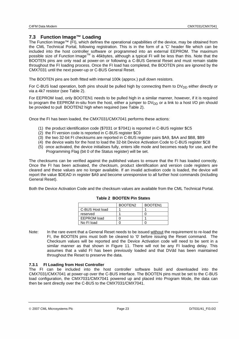
7.3.1 FI Loading from Host Controller The FI can be included into the host controller software build and downloaded into the CMX7031/CMX7041 at power-up over the C-BUS interface. The BOOTEN pins must be set to the C-BUS load configuration, the CMX7031/CMX7041 powered up and placed into Program Mode, the data can then be sent directly over the C-BUS to the CMX7031/CMX7041.
C4FM Data Modem CMX7031/CMX7041
© 2007 CML Microsystems Plc Page 24 D/7031/41_FI3.0/2
BOOTEN2=1BOOTEN1=1
Power-up / Reset CMX7041
Send Start Block 1 Address (DB1_ptr) to C-Bus $B6Send Block 1Length (DB1_len) to C-Bus $B7
Wait for C-Bus $C6 bit 0 to be set to 1Send next data to C-Bus $C8
Verify Checksum values in $A9, $AA and $B8, $B9
Send Device Activation Code hi to $C8
Send Device Activation Code lo to $C8
Wait for C-Bus $C6 bit 0 to be set to 1
CMX7041 is now ready for use
Send Start Block 2 Address (DB2_ptr) to C-Bus $B6Send Block 2 Length (DB2_len) to C-Bus $B7
Wait for C-Bus $C6 bit 0 to be set to 1Send next data to C-Bus $C8
Wait for C-Bus $C6 bit 0 to be set to 1
Send Start Block 3 Address (ACTIVATE_ptr) to C-Bus $B6Send Block 3 Length (ACTIVATE_len) to C-Bus $B7
Wait for C-Bus $C6 bit 0 to be set to 1
Send $0001 to C-Bus $C8
Wait for C-Bus $C6 bit 0 to be set to 1
Send $0001 to C-Bus $C8
Wait for C-Bus $C6 bit 0 to be set to 1
Send $0001 to C-Bus $C8
Wait for C-Bus $C6 bit 0 to be set to 1
note: BOOTEN1 and BOOTEN2 may be changed at
this point, if required
BOOTEN1
BOOTEN2
VDD
Figure 10 FI Loading from Host
The download time is limited by the clock frequency of the C-BUS, with a 5MHz SCLK, it should take less than 500ms to complete (host dependant).
C4FM Data Modem CMX7031/CMX7041
© 2007 CML Microsystems Plc Page 25 D/7031/41_FI3.0/2
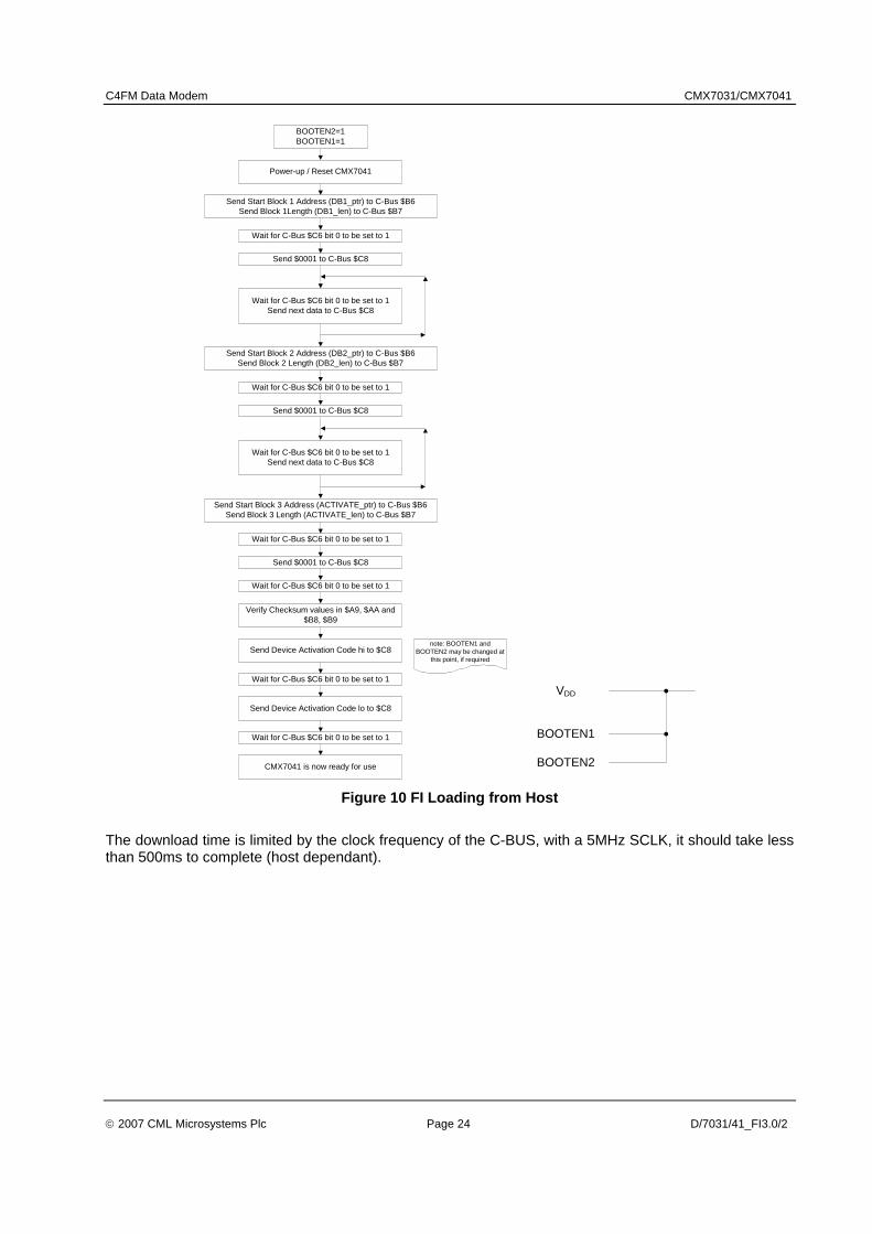
7.3.2 FI Loading from EEPROM The FI must be converted into a format for the EEPROM programmer (normally Intel Hex) and loaded into the EEPROM either by the host or an external programmer. The CMX7031/CMX7041 needs to have the BOOTEN pins set to EEPROM load, and then, on power-on, or following a C-BUS General Reset, the CMX7031/CMX7041 will automatically load the data from the EEPROM without intervention from the host controller.
BOOTEN2=0BOOTEN1=1
Power-up / Reset CMX7041
Verify Checksum values in $A9, $AA and $B8, $B9
Send Device Activation Code hi to $C8
Send Device Activation Code lo to $C8
Wait for C-Bus $C6 bit 0 to be set to 1
CMX7041 is now ready for use
Wait for C-Bus $C6 bit 0 to be set to 1
Wait for C-Bus $C6 bit 0 to be set to 1
note: BOOTEN1 and BOOTEN2 may be changed at
this point, if required
BOOTEN1
BOOTEN2
VDD
Jumper for programming
EEPROM (if required)
Figure 11 FI Loading from EEPROM
The CMX7031/CMX7041 has been designed to function with Atmel AT25HP512 serial EEPROM and the AT25F512 flash EEPROM devices3, however other manufacturers parts may also be suitable. The time taken to load the FI is dependant on the Xtal frequency; with a 6.144MHz Xtal, it should load in less than 1 second. 3 Note that these two memory devices have slightly different addressing schemes. FI3.0 is compatible with both schemes.
C4FM Data Modem CMX7031/CMX7041
© 2007 CML Microsystems Plc Page 26 D/7031/41_FI3.0/2
7.4 Device Control The CMX7031/CMX7041 can be set into the relevant mode to suit its environment. These modes are described in the following sections and are programmed over the C-BUS: either directly to operational registers or, for parameters that are not likely to change during operation, via the Programming register ($C8).
For basic operation:
(1) enable the relevant hardware sections via the Power Down Control register
(2) set the appropriate mode registers to the desired state
(3) select the required Signal Routing and Gain
(4) use the Mode Control register to place the device into Rx or Tx mode.
To conserve power when the device is not actively processing a signal, place the device into Idle mode. Additional powersaving can be achieved by disabling any unused hardware blocks, however, care must be taken not to disturb any sections that are automatically controlled. Note that the BIAS block must be enabled to allow any of the Input or Output blocks to function.
See: o Power Down Control - $C0 write o Modem Control - $C1 write o Modem Config - $C7 write
7.4.1 General Notes In normal operation, the most significant registers, in addition to the TxData and RxData blocks, are:
o Modem Control - $C1 write o Status - $C6 read o Analogue Output Gain - $B0 write o Input Gain and Output Signal Routing - $B1 write o AuxData Write - $C2 write
Setting the Mode register to either Rx or Tx will automatically increase the internal clock speed to its operational speed, whilst setting the Mode register to IDLE will automatically return the internal clock to a lower (powersaving) speed. To access the Program Blocks (through the Programming register, $C8) the device MUST be in IDLE mode.
Under normal circumstances the CMX7031/CMX7041 manages the Main Clock Control automatically, using the default values loaded in Program Block 3.
7.4.2 Interrupt Operation The CMX7031/CMX7041 will issue an interrupt on the IRQN line when the IRQ bit (bit 15) of the Status register and the IRQ Mask bit (bit 15) are both set to 1. The IRQ bit is set when the state of the interrupt flag bits in the Status register change from a 0 to 1 and the corresponding mask bit(s) in the Interrupt Mask register is(are) set. Enabling an interrupt by setting a mask bit (0→1) after the corresponding Status register bit has already been set to 1 will also cause the IRQ bit to be set.
All interrupt flag bits in the Status register, except the Programming Flag (bit 0), are cleared and the interrupt request is cleared following the command/address phase of a C-BUS read of the Status register. The Programming Flag bit is set to 1 only when it is permissible to write a new word to the Programming register.
See:
o Status - $C6 read o Interrupt Mask - $CE write

C4FM Data Modem CMX7031/CMX7041
© 2007 CML Microsystems Plc Page 27 D/7031/41_FI3.0/2
7.4.3 Signal Routing The CMX7031/CMX7041 offers a flexible routing architecture, with three signal inputs, a choice of two modulator configurations (to suit 2-point modulation or I & Q schemes) and a single audio output.
See: o Input Gain and Output Signal Routing - $B1 write o Modem Control - $C1 write o Modem Config - $C7 write
The analogue gain / attenuation of each input and output can be set individually, with additional Fine Attenuation control available via the Programming registers.
See: o Analogue Output Gain - $B0 write o Input Gain and Output Signal Routing - $B1 write
In common with other FIs developed for the CMX7031/CMX7041, this device is equipped with two signal processing paths. However, in this implementation of the FI, Input 2 is not currently used and so should not be enabled. Input 1 should be routed to either of the three input sources (ALT, DISC or MIC). The internal signals Output 1 and 2 are used to provide either 2-point or I & Q signals and should be routed to the MOD1 and MOD2 pins as required.
7.4.4 Modem Control The CMX7031 operates in one of three modes:
o IDLE o Rx o Tx
At power-on or following a Reset, the device will automatically enter IDLE mode, which allows for the maximum powersaving whilst still retaining the capability of monitoring the AuxADC inputs (if enabled). It is only possible to write to the Programming register whilst in IDLE mode.
See: o Modem Control - $C1 write
GPIO1 and 2 pins reflect bits 0 and 1 of the Modem Control register, as shown in Table 3. These can be used to drive external hardware without the host having to intervene. The CMX7041 also has two additional GPIO pins that are programmable under host control.
Table 3 Modem Mode Selection
Modem Control ($C1) b1-0 Modem Mode GPIO2 GPIO1 00 Idle – low power mode 1 1 01 Rx mode 1 0 10 Tx mode 0 1 11 reserved 1 1

C4FM Data Modem CMX7031/CMX7041
© 2007 CML Microsystems Plc Page 28 D/7031/41_FI3.0/2
Table 4 Modem Control Selection
C4FM Modem Control ($C1) b7-4 Rx Tx 0000 idle idle 0001 reserved reserved 0010 Rx C4FM raw Tx C4FM raw 0011 Rx C4FM eye Tx C4FM PRBS 0100 reserved Tx C4FM Preamble 0101 reserved reserved 0110 Sync Test 0111 Reset / abort Reset / abort 1xxx reserved reserved
In Tx mode, the CMX7031/CMX7041 can be set to transmit data in a number of raw data modes as a data pump. The Modem Control bits should be configured in the same C-BUS write as the change in the Modem Mode bits. The Tx C4FM raw command requires that a block of data has been loaded into the C-BUS TxData registers before executing the change in the Modem Mode bits to Tx. A DataRDY IRQ will then be asserted and the host should supply a further 72 bits of payload data in the TxData registers. The CMX7031/CMX7041 will continue transmitting the payload data until the host resets the Mode bits to either Rx or IDLE, as appropriate.
In Rx mode the Rx signal is routed through Input 1. Rx data recovered from the received signal is supplied to the host through the RxData registers and should be read in response to a DataRDY IRQ. The CMX7031/CMX7041 will continue decoding the input waveform until the host resets the Mode bits to either Tx or IDLE, as appropriate. A test mode to examine the Rx “EYE” is also provided.
7.4.5 Tx Mode In Raw mode Tx operation, the preamble and Frame Sync 1 (FS1) are transmitted automatically (default values may be changed by use of the Program Registers), and then data from the TxData Block is transmitted directly until the Mode is changed to Rx or Idle. The first block of data MUST be loaded into the TxData registers BEFORE executing the Modem Mode change to Tx. Data is transmitted MSB first.
The host should write the initial data to the C-BUS TxData registers and then set the modem mode to TxRaw and the Mode bits to Tx. As soon as the data has been read from the C-BUS TxData registers the DataRDY IRQ will be asserted.

C4FM Data Modem CMX7031/CMX7041
© 2007 CML Microsystems Plc Page 29 D/7031/41_FI3.0/2
Load data to C-Bus TxDataBlock
transaction count =0, byte count =9
Set Modem Control toTxRaw, C4FM, Mode = Tx
IRQ = DataRdy?
No
GPIO2 and GPIO1 will change to 10 and the Modem will transmit the preamble, frame sync and data The host should ensure that
any external hardware is also set into Tx mode (if not automatically controlled by the GPIO pins).
note:
yes
more data to send?
Load data to C-Bus TxDataBlock
transaction count ++, byte count =9
yes
No
See Rx_Process flow diagramnote:
Set Modem Control to Idle, C4FM, Mode = Idle
GPIO2 and GPIO1 will change to 00 and the Modem will drop into Idle mode. The
host should ensure that any external hardware is also set into Idle mode (if not
automatically controlled by the GPIO pins).
note:
Goto Rx_Process
Goto Idle Mode
This assumes that:GPIO2 and GPIO1 have been set to mode 10 (follow Mode bits)RAMDAC has been enabledData is in 9 byte blocks
note:
Tx_Process
IRQ = TxDone?
No
Yes
IRQ=Error, Modem status = Underflow may occur at
this point, if enabled.note:
Due to internal processing delays in the filters etc, the Host should wait for IRQ=TxDone or implement its own delay to ensure all data has been transmitted.
note:
Execute RAMDAC down
Execute RAMDAC upEnsure that RAMDAC speed
is fast enough to allow for hardware and internal
processing delays
note:
Figure 12 Tx Data Flow
7.4.6 Rx Mode In Raw mode Rx operation, once a valid Frame Sync (FS) has been detected, all following data received is loaded directly into the C-BUS RxData registers. This will continue until the Mode is changed to Idle or Tx, even if there is no valid signal at the input. On exiting Rx Mode, there may be a DataRdy IRQ pending which should be cleared by the host. Note that Raw Mode operation still requires the use of a valid Frame Sync pattern in order to derive timing information for the demodulator.

C4FM Data Modem CMX7031/CMX7041
© 2007 CML Microsystems Plc Page 30 D/7031/41_FI3.0/2
The device will update the C-BUS RxData registers with Rx payload data as it becomes available, the host MUST respond to the DataRDY IRQ before the RxData registers are over-written by subsequent data from the modem. If “Soft” data mode has been selected, then the Payload Data in Rx mode will be coded as 4-bits of “Log Likelihood Ratio” encoded data per “over-air” bit. In this mode the host must service the DataRDY IRQ and RxData registers at 4 times the normal rate to avoid overflow conditions.
Rx_Process
Set Modem Control to RxRaw, C4FM, Mode = Rx
IRQ = DataRdy?
No
GPIO2 and GPIO1 will change to 01, the Modem will start to look for frame sync. The host should ensure that any external
hardware is also set into Rx mode (if not automatically controlled by the GPIO pins).
note:
yes
more data to receive?
Load data from C-Bus RxDataBlock
check transaction count and byte count
yes
No
See Tx_Process Flow Diagramnote:
Set Modem Control to Idle, C4FM, Mode = Idle
GPIO2 and GPIO1 will change to 00, and the Modem will drop into Idle mode. The
host should ensure that any external hardware is also set into Idle mode (if not
automatically controlled by the GPIO pins).
note:
Goto Tx_Process
Goto Idle_Process
This assumes that:GPIO2 and GPIO1 have been set to mode 10 (follow Mode bits)RAMDAC has been enabledData is in 9 byte blocks
note:
If enabled , IRQ=FrameSync will occur before IRQ=DataRdy
note:
An IRQ=DataRdy may still be
pending at this point
note:
Figure 13 Rx Data Flow
7.4.7 Other Modem Modes In Rx mode it is possible to output the received signal as an “EYE” diagram for test and alignment purposes. In this configuration, the filtered received signal is presented at the MOD1 pin and a trigger pulse at the MOD2 pin (derived directly from the xtal / clock source) to allow viewing on a suitable oscilloscope.
In Tx mode, a fixed PRBS sequence or a fixed preamble transmission is provided to facilitate test and alignment.
7.4.8 Data Transfer The payload data is transferred to and from the host via a block of five Rx and Tx 16-bit C-BUS registers which allow up to 72 bits (9 bytes) of data to be transferred in sequence. The lowest 8 bits of the register block are reserved for a Byte Counter, Block ID and a Transaction Counter to allow the host to identify

C4FM Data Modem CMX7031/CMX7041
© 2007 CML Microsystems Plc Page 31 D/7031/41_FI3.0/2
any data loss, and the remaining 72 bits hold the data to be transmitted / received. The byte count indicates how many bytes in the data block are valid and so reduces the need to perform a full 5 word C-BUS read / write if only small blocks of data need to be transferred.
Table 5 C-BUS Data Registers
C-BUS Address Function C-BUS address Function $B5 Tx data 0-7 & info $B8 Rx data 0-7 & info $B6 Tx data 8-23 $B9 Rx data 8-23 $B7 Tx data 24-39 $BA Rx data 24-39 $CA Tx data 40-55 $BB Rx data 40-55 $CB Tx data 56-71 $C5 Rx data 56-71
The Block ID is ignored in Raw Data mode, but should be set to 01 for consistency with future enhancements. Bits 7 and 6 hold a Transaction Counter. This is a two-bit counter that is incremented on every read / write of the Data Block. This is particularly useful to detect data underflow and overflow conditions. The counter increments modulo 4. The host must increment this counter on every write to the TxData block. If the CMX7031/CMX7041 identifies that a block has been written out of sequence, the Error IRQ will be asserted. The device detects that new data from the host is available by the change in the value of the Transaction Counter, therefore the host should ensure that all the data is available in the TxData block before updating this register (ie, it should be the last register the host writes to in any block transfer). In Rx mode, the CMX7031/CMX7041 will automatically increment the counter every time it writes to the RxData block, if the host identifies that a block has been written out of sequence, then it is likely that a data overrun condition has occurred and some data has been lost.
7.5 Squelch Operation Many Limiter / Discriminator chips provide a noise-quieting squelch circuit around an op-amp configured as a filter. This signal is conventionally passed to a comparator to provide a digital Squelch signal, which can be routed directly to one of the CMX7031/CMX7041’s GPIO pins or to the host. However with the CMX7031/CMX7041, the comparator and threshold operations can be replaced by one of the AuxADC’s with programmable thresholds and hysteresis functions.
See: o Status - $C6 read o Modem Config - $C7 write
7.6 GPIO Pin Operation The CMX7031 provides 2 GPIO pins, the CMX7041 provides 4 GPIO pins. GPIO1 and 2 can be configured to reflect the Tx / Rx state of the Mode Register (TxENA and RxENA).
See: o Modem Config - $C7 write
Note that when GPIO1 and 2 are in modes 10 and 11, they will not change state until the relevant Mode change has been executed. This is to allow the host sufficient time to load the relevant data buffers and the CMX7031 time to encode the data required prior to its transmission.

C4FM Data Modem CMX7031/CMX7041
© 2007 CML Microsystems Plc Page 32 D/7031/41_FI3.0/2
7.7 Auxiliary ADC Operation The inputs to the two Auxiliary ADCs can be independently routed from any of the Signal Input pins under control of the Signal Routing register, $A7. Conversions will be performed as long as a valid input source is selected, to stop the ADCs, the input source should be set to “none”. Register $C0, b6, BIAS, must be enabled for Auxiliary ADC operation.
Averaging can be applied to the ADC readings by selecting the relevant bits in the Signal Routing register, $A7, the length of the averaging is determined by the value in the Programming register (P3.0 and P3.1), and defaults to a value of 1. This is a rolling average system such that a proportion of the current data will be added to the last value. The proportion is determined by the value of the average counter in P3.0 and P3.1.
For an average value of:
0 then 50% of the current value will be added to 50% of the last value,
1 = 25% of the current value will be added to 75% of the last value,
2 = 12.5% etc.
The maximum useful value of this field is 8.
High and Low thresholds may be independently applied to both ADC channels (the comparison is applied after averaging, if this is enabled) and an IRQ generated as required (except in the case where the high threshold has been set below the low threshold). The thresholds are programmed via the AuxADC Threshold register, $B5.
Auxiliary ADC data is read back in the AuxADC Data registers ($A9 and $AA) and includes the threshold status as well as the actual conversion data (subject to averaging, if enabled).
See: o AuxADC config - $A7 write o AuxADC1 data - $A9 read o AuxADC2 data - $AA read o AuxADC threshold data - $CD write
7.8 Auxiliary DAC / RAMDAC Operation The four Auxiliary DAC channels are programmed via the AuxDAC Control register, $A8. AuxDAC channel 1 may also be programmed to operate as a RAMDAC which will automatically output a pre-programmed profile at a programmed rate. The AuxDAC Control register, $A8, with b12 set, controls this mode of operation. The default profile is a raised cosine (see Table 8), but this may be over-written with a user- defined profile by writing to Programming register P3.11. The RAMDAC operation is only available in Tx mode and, to avoid glitches in the ramp profile, it is important not to change to IDLE or Rx mode whilst the RAMDAC is still ramping. The AuxDAC outputs hold the user-programmed level during a powersave operation if left enabled, otherwise they will return to zero. Note that access to all four AuxDACs is controlled by the AuxDAC Control register, $A8, and therefore to update all AuxDACs requires four writes to this register. It is not possible to simultaneously update all four AuxDACs.
See: o AuxDAC control / data - $A8 write
7.9 RF Synthesisers (CMX7031 only) The CMX7031 includes two Integer-N RF synthesisers, each comprising a divider, phase comparator and charge pump. The divider has two sets of N and R registers: one set can be used for transmit and the other for receive. The division ratios can be set up in advance by means of C-BUS registers. A single C-BUS command will change over from the transmit to the receive division ratios, or vice versa, enabling a fast turnaround between Rx and Tx settings.

C4FM Data Modem CMX7031/CMX7041
© 2007 CML Microsystems Plc Page 33 D/7031/41_FI3.0/2
See: o RF Channel Data - $B2 write o RF Channel Control - $B3 write o RF Channel Status - $B4 8-bit read
External RF components are needed to complete the synthesiser circuit. A typical schematic for one synthesiser, with external components, is shown in Figure 14.
Figure 14 Example RF Synthesiser Components for a 512MHz Receiver
R31 0Ω C31 820pF R32 18kΩ C32 8.2nF R33 18kΩ C33 680pF
C34 1nF C35 1nF
Resistors ±5%, capacitors and inductors ±20% unless otherwise stated.
Note: R31 is chosen within the range 0Ω to 30kΩ and selects the nominal charge pump current.
It is recommended that C34 and C35 are kept close to the VCO and that the stub from the VCO to the CMX7031 / CMX7041 is kept as short as possible. The loop filter components should be placed close to the VCO.

C4FM Data Modem CMX7031/CMX7041
© 2007 CML Microsystems Plc Page 34 D/7031/41_FI3.0/2
Figure 15 Single RF Channel Block Diagram
The two RF synthesisers are programmable to any frequency in the range 100MHz to 600MHz. Figure 15 is a block diagram of one synthesiser channel. The RF synthesiser clock is selectable between the XTAL or the clock supplied to the RF CLOCK input pin. The RF synthesiser clock is common to both channels. The charge pump supply (CP supply, CPVDD) is also common to both channels. The +/-RF in pins, Cpout, Iset and RFVSS pins are channel specific and designated as either RF1+, RF1-, CP1OUT, ISET1, RFVSS or RF2+, RF2-, CP2OUT, ISET2, RFVSS on the Signal List in section 3. The N and R values for Tx and Rx modes are channel specific and can be set from the host µC via the C-BUS. Various channel specific status signals are also accessible via C-BUS. The divide by N counter is 20 bits; the R counter is 13 bits. Typical external components are shown in Figure 14.
Both synthesisers are phase locked loops (PLLs) of the same design, utilising external VCOs and loop filters. The VCOs need to have good phase noise performance although it is likely that the high division ratios used will result in the dominant noise source being the reference oscillator. The phase detectors are of the phase-frequency type with a high impedance charge pump output requiring just passive components in the loop filter. Lock detect functions are built in to each synthesiser and the status reported via C-BUS. A transition to out-of-lock can be detected and communicated via a C-BUS interrupt to the host µC. This can be important in ensuring that the transmitter cannot transmit in the event of a fault condition arising.
Two levels of charge pump gain are available to the user, to facilitate the possibility of locking at different rates under program control. A current setting resistor (R31) is connected between the ISET pin (one for each PLL system) and the respective RFVSS. This resistor will have an internally generated band gap voltage expressed across it and may have a value of 0Ω to 30kΩ, which (in conjunction with the on-chip series resistor of 9.6kΩ) will give charge pump current settings over a range of 2.5mA down to 230µA (including the control bit variation of 4 to 1). The value of the current setting resistor (R31) is determined in accordance with the following formulae:
gain bit set to 1: R31 (in Ω) = (24/Icp) – 9600 gain bit cleared to 0: R31 (in Ω) = (6/Icp) – 9600 where Icp is the charge pump current (in mA).
Note that the charge pump current should always be set to at least 230µA. The ‘gain bit’ refers to either bit 3 or bit 11 in the RF Channel Control register, $B3.
Divide by N counter
Lock detect
Divide by R counter
Charge Pump
Voltage Ref
Phase Comp
-
+
- RF in
+ RF in
RF synthesiser clock
Mux
Mux
TX N RX N
TX R RX R
CP out
CP supply
I set
Internal Clock

C4FM Data Modem CMX7031/CMX7041
© 2007 CML Microsystems Plc Page 35 D/7031/41_FI3.0/2
The step size (comparison frequency) is programmable; to minimise the effects of phase noise this should be kept as high as possible. This can be set as low as 2.5kHz (for a reference input of 20MHz or less), or up to 200kHz – limited only by the performance of the phase comparator. The frequency for each synthesiser is set by using two registers: an ‘R’ register that sets the division value of the input reference frequency to the comparison frequency (step size), and an ‘N’ register that sets the division of the required synthesised frequency from the external VCO to the comparison frequency. This yields the required synthesised frequency (Fs), such that:
Fs = (N / R) x FREF where FREF is the selected reference frequency
Other parameters for the synthesisers are the charge pump setting (high or low)
o Since the set-up for the PLLs takes 4 x “RF Channel Data register” writes it follows that, while updating the PLL settings, the registers may contain unwanted or intermediate values of bits. These will persist until the last register is written. It is intended that users should change the content of the “RF Channel Data register” on a PLL that is disabled, powersaved or selected to work from the alternate register set (“Tx” and “Rx” are alternate register sets). There are no interlocks to enforce this intention. The names “Tx” and “Rx” are arbitrary and may be assigned to other functions as required. They are independent sets of registers, one of which is selected to command each PLL by changing the settings in the RF Channel Control - $B3 write register.
For optimum performance, a common master clock should be used for the RF synthesisers (RF Clock) and the baseband sections (Main and Auxiliary System Clocks). Using unsynchronised clocks can result in spurious products being generated in the synthesiser output and in some cases difficulty may be experienced with obtaining lock in the RF synthesisers.
Lock Status The lock status can be observed by reading the RF Channel Status register, $B4, and the individual lock status bits can (subject to masking) provide a C-BUS interrupt.
The lock detector can use a tolerance of one cycle or four cycles of the reference clock (not the divided version that is used as a comparison frequency) in order to judge phase lock. An internal shift register holds the last three lock status measurements and the lock status bits are flagged according to a majority vote of these previous three states. Hence, one occasional lock error will not flag a lock fail. At least two successive phase lock events are required for the lock status to be true. Note that the lock status bits confirm phase lock to the measured tolerance and not frequency lock. The synthesiser may take more time to confirm phase lock with the lock status bits than the time to switch from channel to channel. The purpose of a 4-cycle tolerance is for the case where a high frequency reference oscillator would not forgive a small phase error.
RF Inputs The RF inputs are differential and self biased (when not powersaved). They are intended to be capacitatively coupled to the RF signal. The signal should be in the range 0dBm to –20dBm (not necessarily balanced). To ensure an accurate input signal the RF should be terminated with 50Ω as close to the chip as possible and with the “+” and “–“ inputs capacitatively coupled to the input and ground, keeping these connections as short as possible. The RF input impedance is almost purely capacitative and is dominated by package and printed circuit board parasitics.
Guidelines for using the RF Synthesisers • RF input slew rate (dv/dt) should be 14 V/µs minimum. • The RF Synthesiser 2.5V digital supply can be powered from the VDEC output pin. • RF clock sources and other, different clock sources must not share common IC components, as this
may introduce coupling into the RF. Unused ac-coupled clock buffer circuits should be tied off to a dc supply, to prevent them oscillating.
• It is recommended that the RF Synthesisers are operated with maximum gain Iset (ie. Iset tied to RFVss).
• The Loop components should be optimised for each VCO.

C4FM Data Modem CMX7031/CMX7041
© 2007 CML Microsystems Plc Page 36 D/7031/41_FI3.0/2
7.10 Digital System Clock Generators
Ref CLK div/1 to 512$AC b0-8
PD
VCO
PLL div/1 to 1024$AB b0-9
LPF
SysCLK1Ref
SysCLK1Div
VCO op div/1 to 64
$AB b10-15SysCLK1Pre-CLK
$AC b11-15
SysCLK1Output
384kHz-20MHz
48 - 192kHz(96kHz typ)
SysCLK1 VCO24.576-
98.304MHz(49.152MHz typ)
Ref CLK div/1 to 512$AE b0-8
PD
VCO
PLL div/1 to 1024$AD b0-9
LPF
SysCLK2Ref
SysCLK2Div
VCO op div/1 to 64
$AD b10-15SysCLK2Pre-CLK
$AE b11-15
SysCLK2Output
384kHz-20MHz
48 - 192kHz(96kHz typ)
SysCLK2 VCO24.576-
98.304MHz(49.152MHz typ)
Ref CLK div/1 to 512$BD b0-8
PD
VCO
PLL div/1 to 1024$BC b0-9
LPF
MainCLKRef
MainCLKDiv
VCO op div/1 to 64
$BC b10-15MainCLKPre-CLK
$BD b11-15
MainCLKOutput
384kHz-50MHz(24.576MHz typ)
48 - 192kHz(96kHz typ)
MainCLK VCO24.576-
98.304MHz(49.152MHz typ)
To InternalADC / DAC
dividers
AuxADCDiv
Aux_ADC(83.3kHz typ)
OSC4.0 - 12.288MHz Xtal
or4.0 - 24.576MHZ Clock
to RF SynthesiserRef CLK selection
Figure 16 Digital Clock Generation Schemes
The CMX7031/CMX7041 includes a 2-pin crystal oscillator circuit. This can either be configured as an oscillator, as shown in section 5, or the XTAL input can be driven by an externally generated clock. The crystal (Xtal) source frequency can go up to 12.288MHz (clock source frequency up to 24.576MHz), but a 6.144MHz Xtal is assumed by default for the functionality provided in the CMX7031/CMX7041.

C4FM Data Modem CMX7031/CMX7041
© 2007 CML Microsystems Plc Page 37 D/7031/41_FI3.0/2
7.10.1 Main Clock Operation A digital PLL is used to create the Main Clock (nominally 24.576MHz) for the internal sections of the CMX7031/CMX7041. At the same time, other internal clocks are generated by division of either the XTAL Reference Clock or the Main Clock. These internal clocks are used for determining the sample rates and conversion times of A-to-D and D-to-A converters, running a General Purpose Timer and the signal processing block. In particular, it should be noted that in IDLE mode the setting of the GP Timer divider directly affects the C-BUS latency (with the default values this is nominally 250µs).
The CMX7031/CMX7041 defaults to the settings appropriate for a 6.144MHz Xtal, however if other frequencies are to be used then the Program Block registers P3.2 to P3.6 will need to be programmed appropriately at power-on. This flexibility allows the device to re-use an external clock source, so reducing total cost and potential noise sources. A table of common values is provided in Table 1. The C-BUS registers $BC and $BD are controlled automatically by the FI and must not be accessed directly by the user.
See: o Program Block 3 – AuxDAC, RAMDAC and Clock control
7.10.2 System Clock Operation Two System Clock outputs, SysClock1 Out and SysClock2 Out, are available to drive additional circuits, as required. These are digital phase locked loop (PLL) clocks that can be programmed via the System Clock registers with suitable values chosen by the user. The System Clock PLL Configure registers ($AB and $AD) control the values of the VCO Output divider and Main Divide registers, while the System Clock Ref. Configure registers ($AC and $AE) control the values of the Reference Divider and signal routing configurations. The PLLs are designed for a reference frequency of 96kHz. If not required, these clocks can be independently powersaved. The clock generation scheme is shown in the block diagram of Figure 16. Note that at power-on, these pins provide, by default, a clock which is equivalent to the XTAL frequency, however in the CMX7041, the output is inhibited until enabled by a host command over the C-BUS.
See: o System CLK 1 and 2 PLL data - $AB, $AD write o System CLK 1 and 2 REF - $AC and $AE write
7.11 Signal Level Optimisation The internal signal processing of the CMX7031/CMX7041 will operate with wide dynamic range and low distortion only if the signal level at all stages in the signal processing chain is kept within the recommended limits. For a device working from a 3.3V ±10% supply, the maximum signal level which can be accommodated without distortion is [(3.3 x 90%) - (2 x 0.3V)] Volts pk-pk = 838mV rms, assuming a sine wave signal. This should not be exceeded at any stage.
7.11.1 Transmit Path Levels For the maximum signal out of the MOD1 and MOD2 attenuators, the signal level at the output of the Modem block is set to be 0dB, The Fine Output adjustment has a maximum attenuation of 1.8dB and no gain, whereas the Coarse Output adjustment has a variable attenuation of up to +44.8dB and no gain.
7.11.2 Receive Path Levels The Fine Input adjustment has a maximum attenuation of 3.5dB and no gain, whereas the Coarse Input adjustment has a variable gain of up to +22.4dB and no attenuation. With the lowest gain setting (0dB), the maximum allowable input signal level at the DiscFB pin would be 883mV rms. This signal level is an absolute maximum, which should not be exceeded anywhere in the signal processing chain if severe distortion is to be avoided.
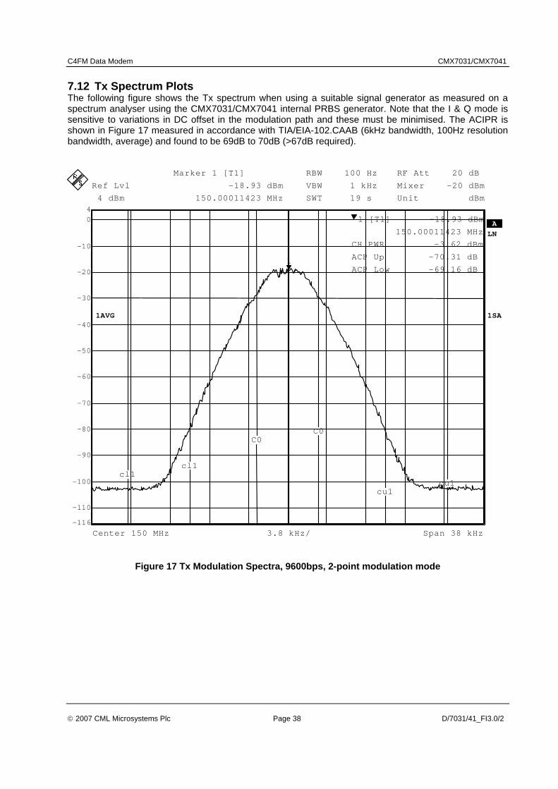
C4FM Data Modem CMX7031/CMX7041
© 2007 CML Microsystems Plc Page 38 D/7031/41_FI3.0/2
7.12 Tx Spectrum Plots The following figure shows the Tx spectrum when using a suitable signal generator as measured on a spectrum analyser using the CMX7031/CMX7041 internal PRBS generator. Note that the I & Q mode is sensitive to variations in DC offset in the modulation path and these must be minimised. The ACIPR is shown in Figure 17 measured in accordance with TIA/EIA-102.CAAB (6kHz bandwidth, 100Hz resolution bandwidth, average) and found to be 69dB to 70dB (>67dB required).
R e f L v l 4 d B m R e f L v l 4 d B m
A LNLN
C e n t e r 1 5 0 M H z S p a n 3 8 kHz
RBW 100 HzVBW 1 kHzSWT 19 s
M i x e r - 2 0 dBmU n i t dBm
3.8 kHz/
R F A t t 2 0 dB
1SA1 A V G
- 1 1 0
- 1 0 0
- 9 0
- 8 0
- 7 0
- 6 0
- 5 0
- 4 0
- 3 0
- 2 0
- 1 0
0
- 1 1 6
4
1
M a r k e r 1 [ T1] -18.93 dBm 1 5 0 . 0 0 011423 MHz
1 [T1] - 1 8 . 9 3 dBm 1 5 0 . 0 0 0 1 1 4 2 3 MHzCH PWR - 3 . 6 2 dBmACP Up - 7 0 . 3 1 dB ACP Low - 6 9 . 1 6 dB
cu1c u 1
c l 1 c l 1
C0C0
Figure 17 Tx Modulation Spectra, 9600bps, 2-point modulation mode

C4FM Data Modem CMX7031/CMX7041
© 2007 CML Microsystems Plc Page 39 D/7031/41_FI3.0/2
7.13 C-BUS Register Summary Table 6 C-BUS Registers
ADDR. (hex) REGISTER Word Size
(bits) $01 W C-BUS RESET 0
$A7 W AuxADC Config 16 $A8 W AuxDAC Data and Control 16 $A9 R AuxADC1 Data and Status / Checksum 2 hi 16 $AA R AuxADC2 Data and Status / Checksum 2 lo 16 $AB W System Clk 1 PLL configure 16 $AC W System Clk 1 Ref configure 16 $AD W System Clk 2 PLL configure 16 $AE W System Clk 2 Ref configure 16 $AF Reserved
$B0 W Analog Output Gain 16 $B1 W Input Gain and Signal Routing 16 $B2 Reserved $B3 Reserved $B4 Reserved $B5 W TxData 0 16 $B6 W TxData 1 16 $B7 W TxData 2 16 $B8 R RxData 0 / Checksum 1 hi 16 $B9 R RxData 1 / Checksum 1 lo 16 $BA R RxData 2 16 $BB R RxData 3 16 $BC W Main CLK PLL configure – reserved 16 $BD W Main CLK Ref configure – reserved 16 $BE Reserved $BF Reserved
$C0 W Power-Down Control 16 $C1 W Mode Control 16 $C2 W AuxData write 16 $C3 Reserved $C5 R Rx Data 4 16 $C6 R IRQ Status 16 $C7 W Modem Config 16 $C8 W Programming Register 16 $C9 R Modem Status 16 $CA W Tx Data 3 16 $CB W Tx Data 4 16 $CC R AuxData read 16 $CD W AuxADC Thresholds 16 $CE W Interrupt Mask 16 $CF Reserved
All other C-BUS addresses (including those not listed above) are either reserved for future use or allocated for production testing and must not be accessed in normal operation.

C4FM Data Modem CMX7031/CMX7041
© 2007 CML Microsystems Plc Page 40 D/7031/41_FI3.0/2
8 Performance Specification 8.1 Electrical Performance 8.1.1 Absolute Maximum Ratings Exceeding these maximum ratings can result in damage to the device. Min. Max. Unit Supply: DVDD- DVSS −0.3 4.5 V
AVDD- AVSS −0.3 4.5 V Voltage on any pin to DVSS −0.3 DVDD + 0.3 V Voltage on any pin to AVSS −0.3 AVDD + 0.3 V Current into or out of any power supply pin (excluding VBIAS) ( i.e. VDEC, AVDD, AVSS, DVDD or DVSS)
−30 +30 mA
Current into or out of any other pin −20 +20 mA Voltage differential between power supplies:
DVDD and AVDD 0 0.3 V DVSS and AVSS 0 50 mV
L9 Package (64-pin LQFP) Min. Max. Unit Total Allowable Power Dissipation at Tamb = 25°C – 668 mW
... Derating – 6 mW/°C Storage Temperature −55 +125 °C Operating Temperature −40 +85 °C Q1 Package (64-pin VQFN) Min. Max. Unit Total Allowable Power Dissipation at Tamb = 25°C – 1410 mW
... Derating – 14 mW/°C Storage Temperature −55 +125 °C Operating Temperature −40 +85 °C L4 Package (48-pin LQFP) Min. Max. Unit Total Allowable Power Dissipation at Tamb = 25°C – 668 mW
... Derating – 6 mW/°C Storage Temperature −55 +125 °C Operating Temperature −40 +85 °C Q3 Package (48-pin VQFN) Min. Max. Unit Total Allowable Power Dissipation at Tamb = 25°C – 1410 mW
... Derating – 14 mW/°C Storage Temperature −55 +125 °C Operating Temperature −40 +85 °C
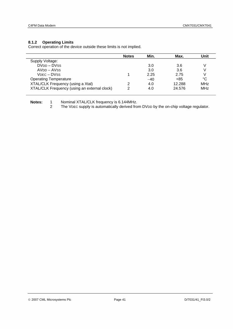
C4FM Data Modem CMX7031/CMX7041
© 2007 CML Microsystems Plc Page 41 D/7031/41_FI3.0/2
8.1.2 Operating Limits Correct operation of the device outside these limits is not implied. Notes Min. Max. Unit Supply Voltage: DVDD – DVSS 3.0 3.6 V AVDD – AVSS 3.0 3.6 V VDEC – DVSS 1 2.25 2.75 V Operating Temperature −40 +85 °C XTAL/CLK Frequency (using a Xtal) 2 4.0 12.288 MHz XTAL/CLK Frequency (using an external clock) 2 4.0 24.576 MHz Notes: 1 Nominal XTAL/CLK frequency is 6.144MHz. 2 The VDEC supply is automatically derived from DVDD by the on-chip voltage regulator.
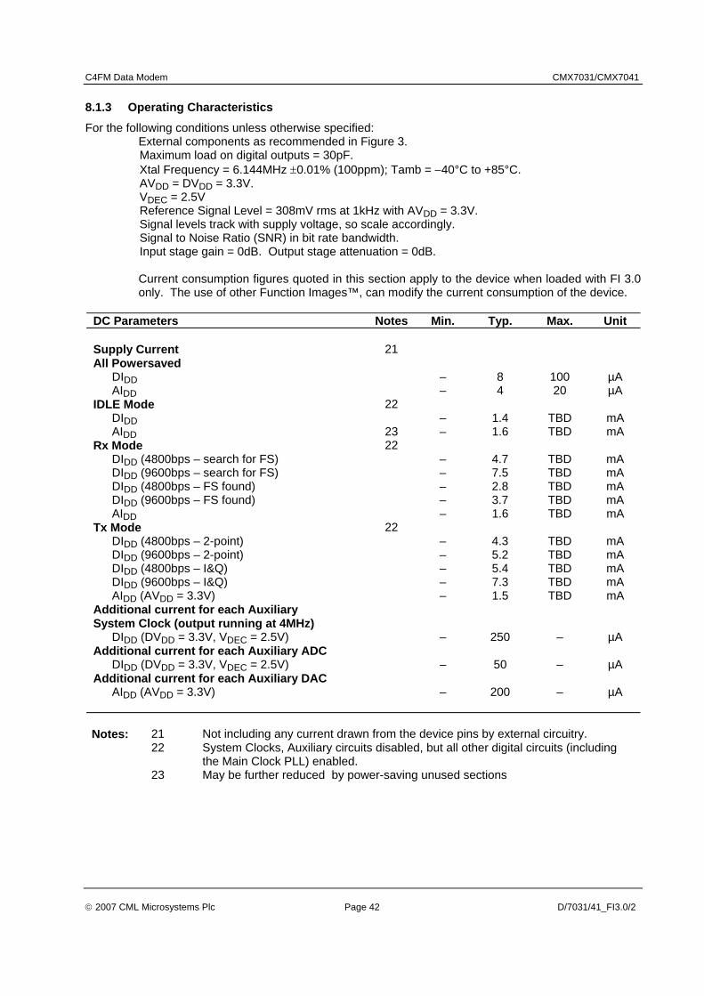
C4FM Data Modem CMX7031/CMX7041
© 2007 CML Microsystems Plc Page 42 D/7031/41_FI3.0/2
8.1.3 Operating Characteristics
For the following conditions unless otherwise specified: External components as recommended in Figure 3. Maximum load on digital outputs = 30pF. Xtal Frequency = 6.144MHz ±0.01% (100ppm); Tamb = −40°C to +85°C. AVDD = DVDD = 3.3V. VDEC = 2.5V Reference Signal Level = 308mV rms at 1kHz with AVDD = 3.3V. Signal levels track with supply voltage, so scale accordingly. Signal to Noise Ratio (SNR) in bit rate bandwidth. Input stage gain = 0dB. Output stage attenuation = 0dB. Current consumption figures quoted in this section apply to the device when loaded with FI 3.0 only. The use of other Function Images™, can modify the current consumption of the device.
DC Parameters Notes Min. Typ. Max. Unit Supply Current 21 All Powersaved DIDD – 8 100 µA AIDD – 4 20 µA IDLE Mode 22 DIDD – 1.4 TBD mA AIDD 23 – 1.6 TBD mA Rx Mode 22 DIDD (4800bps – search for FS) – 4.7 TBD mA DIDD (9600bps – search for FS) – 7.5 TBD mA DIDD (4800bps – FS found) – 2.8 TBD mA DIDD (9600bps – FS found) – 3.7 TBD mA AIDD – 1.6 TBD mA Tx Mode 22 DIDD (4800bps – 2-point) – 4.3 TBD mA DIDD (9600bps – 2-point) – 5.2 TBD mA DIDD (4800bps – I&Q) – 5.4 TBD mA DIDD (9600bps – I&Q) – 7.3 TBD mA AIDD (AVDD = 3.3V) – 1.5 TBD mA Additional current for each Auxiliary System Clock (output running at 4MHz)
DIDD (DVDD = 3.3V, VDEC = 2.5V) – 250 – µA Additional current for each Auxiliary ADC DIDD (DVDD = 3.3V, VDEC = 2.5V) – 50 – µA Additional current for each Auxiliary DAC AIDD (AVDD = 3.3V) – 200 – µA
Notes: 21 Not including any current drawn from the device pins by external circuitry. 22 System Clocks, Auxiliary circuits disabled, but all other digital circuits (including
the Main Clock PLL) enabled. 23 May be further reduced by power-saving unused sections
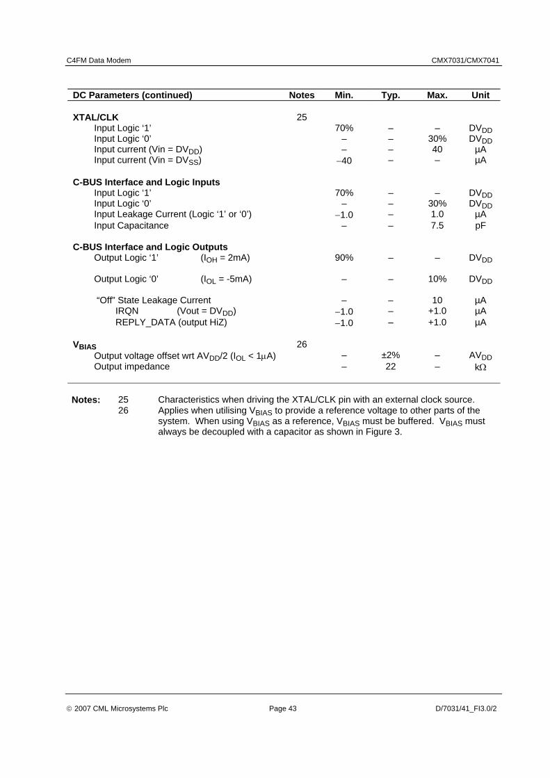
C4FM Data Modem CMX7031/CMX7041
© 2007 CML Microsystems Plc Page 43 D/7031/41_FI3.0/2
DC Parameters (continued) Notes Min. Typ. Max. Unit XTAL/CLK 25
Input Logic ‘1’ 70% – – DVDD Input Logic ‘0’ – – 30% DVDD Input current (Vin = DVDD) – – 40 µA Input current (Vin = DVSS) −40 – – µA
C-BUS Interface and Logic Inputs
Input Logic ‘1’ 70% – – DVDD Input Logic ‘0’ – – 30% DVDD Input Leakage Current (Logic ‘1’ or ‘0’) −1.0 – 1.0 µA Input Capacitance – – 7.5 pF
C-BUS Interface and Logic Outputs
Output Logic ‘1’ (IOH = 2mA) 90% – – DVDD Output Logic ‘0’ (IOL = -5mA) – – 10% DVDD “Off” State Leakage Current – – 10 µA
IRQN (Vout = DVDD) −1.0 – +1.0 µA REPLY_DATA (output HiZ) −1.0 – +1.0 µA
VBIAS 26
Output voltage offset wrt AVDD/2 (IOL < 1µA) – ±2% – AVDD Output impedance – 22 – kΩ
Notes: 25 Characteristics when driving the XTAL/CLK pin with an external clock source. 26 Applies when utilising VBIAS to provide a reference voltage to other parts of the
system. When using VBIAS as a reference, VBIAS must be buffered. VBIAS must always be decoupled with a capacitor as shown in Figure 3.
C4FM Data Modem CMX7031/CMX7041
© 2007 CML Microsystems Plc Page 44 D/7031/41_FI3.0/2
AC Parameters Notes Min. Typ. Max. Unit XTAL/CLK Input
'High' pulse width 31 15 – – ns 'Low' pulse width 31 15 – – ns Input impedance (at 6.144MHz)
Powered-up Resistance – 150 – kΩ Capacitance – 20 – pF Powered-down Resistance – 300 – kΩ Capacitance – 20 – pF
Xtal start up (from powersave) – 20 – ms Auxiliary System Clk 1/2 Outputs
XTAL/CLK input to CLOCK_OUT timing: (in high to out high) 32 – 15 – ns (in low to out low) 32 – 15 – ns 'High' pulse width 33 76 81.38 87 ns 'Low' pulse width 33 76 81.38 87 ns
VBIAS Start up time (from powersave) – 30 – ms
Microphone, Alternative and Discriminator Inputs (MIC, ALT, DISC)
Input impedance 34 – 1 – MΩ Maximum Input Level (pk-pk) 35 – – 80% AVDD Load resistance (feedback pins) 80 – – kΩ Amplifier open loop voltage gain ⎫
(I/P = 1mV rms at 100Hz) ⎭ – 80 – dB Unity gain bandwidth – 1.0 – MHz Programmable Input Gain Stage 36 Gain (at 0dB) 37 −0.5 0 +0.5 dB Cumulative Gain Error ⎫
(wrt attenuation at 0dB) ⎭ 37 −1.0 0 +1.0 dB
Notes: 31 Timing for an external input to the XTAL/CLK pin. 32 XTAL/CLK input driven by an external source. 33 6.144MHz XTAL fitted and 6.144MHz output selected. 34 With no external components connected 35 Centered about AVDD/2; after multiplying by the gain of input circuit (with external
components connected). 36 Gain applied to signal at output of buffer amplifier: DiscFB, AltFB or MicFB 37 Design Value. Overall attenuation input to output has a tolerance of 0dB ±1.0dB

C4FM Data Modem CMX7031/CMX7041
© 2007 CML Microsystems Plc Page 45 D/7031/41_FI3.0/2
AC Parameters Notes Min. Typ. Max. Unit Modulator Outputs 1/2 and Audio Output (MOD 1, MOD 2, AUDIO)
Power-up to output stable 41 – 50 100 µs Modulator Attenuators Attenuation (at 0dB) 43 −1.0 0 +1.0 dB Cumulative Attenuation Error ⎫
(wrt attenuation at 0dB) ⎭ −0.6 0 +0.6 dB Output Impedance ⎫ Enabled 42 – 600 – Ω ⎭ Disabled 42 – 500 – kΩ Output current range (AVDD = 3.3V) – – ±125 µA Output voltage range 44 0.5 – AVDD –0.5 V Load resistance 20 – – kΩ Audio Attenuator Attenuation (at 0dB) 43 −1.0 0 +1.0 dB Cumulative Attenuation Error ⎫
(wrt attenuation at 0dB) ⎭ −1.0 0 +1.0 dB Output Impedance ⎫ Enabled 42 – 600 – Ω ⎭ Disabled 42 – 500 – kΩ Output current range (AVDD = 3.3V) – – ±125 µA Output voltage range 44 0.5 – AVDD –0.5 V Load resistance 20 – – kΩ
Notes: 41 Power-up refers to issuing a C-BUS command to turn on an output. These limits
apply only if VBIAS is on and stable. At power supply switch-on, the default state is for all blocks, except the XTAL and C-BUS interface, to be in placed in powersave mode.
42 Small signal impedance, at AVDD = 3.3V and Tamb = 25°C. 43 With respect to the signal at the feedback pin of the selected input port. 44 Centered about AVDD/2; with respect to the output driving a 20kΩ load to AVDD/2.
C4FM Data Modem CMX7031/CMX7041
© 2007 CML Microsystems Plc Page 46 D/7031/41_FI3.0/2
AC Parameters (cont.) Notes Min. Typ. Max. Unit Auxiliary Signal Inputs (Aux ADC 1 to 4)
Source Output Impedance 51 – – 24 kΩ
Auxiliary 10 Bit ADCs Resolution – 10 – Bits Maximum Input Level (pk-pk) 54 – – 80% AVDD Conversion time 52 – 62.4 – µs Input impedance
Resistance – 10 – MΩ Capacitance – 5 – pF
Zero error ⎫ (input offset to give ADC output = 0) ⎭ 0 – ±10 mV
Integral Non-linearity – – ±3 LSBs Differential Non-linearity 53 – – ±1 LSBs
Auxiliary 10 Bit DACs Resolution – 10 – Bits Maximum Output Level (pk-pk), no load 54 80% – – AVDD Zero error ⎫
(output offset from a DAC input = 0) ⎭ 0 – ±10 mV Resistive Load 5 – – kΩ Integral Non-linearity – – ±4 LSBs Differential Non-linearity 53 – – ±1 LSBs
Notes: 51 Denotes output impedance of the driver of the auxiliary input signal, to ensure
< 1 bit additional error under nominal conditions. 52 With an auxiliary clock frequency of 6.144MHz. 53 Guaranteed monotonic with no missing codes. 54 Centred about AVDD/2.
C4FM Data Modem CMX7031/CMX7041
© 2007 CML Microsystems Plc Page 47 D/7031/41_FI3.0/2
AC Parameters (cont.) Notes Min. Typ. Max. Unit RF Synthesisers – Phase Locked Loops 61,66 Reference Clock Input Input Logic ‘1’ 62 70% – – RFVDD Input Logic ‘0’ 62 – – 30% RFVDD Frequency 5.0 19.2 40.0 MHz Divide ratios (R) 63 1 – 8192
Each RF Synthesiser 69 Comparison frequency 64 – – 500 kHz Input frequency range 67 100 – 600 MHz Input level (at 600MHz) −15 – 0 dBm Input Slew Rate 14 – – V/µs Divide ratios (N) 68 1088 – 104857
5
Oscillator Output Voltage (into 50Ω load) −5 – – dBm Phase Noise Floor – −158 – dBc/Hz Charge pump current (high) 65 ±1.88 ±2.5 ±3.3 mA Charge pump current (low) 65 ±470 ±625 ±820 µA Charge pump current – voltage variation – 10% – per V Charge pump current – sink to source match – 5% – of ISET
Notes: 61 Parameters only guaranteed for the L9 package. 62 Square wave input. 63 Separate dividers provided for each PLL. 64 For optimum performance of the synthesiser subsystems, a common master
clock should be used for the RF Synthesisers and the baseband sections. Using unsynchronised clocks is likely to result in spurious products being generated in the synthesiser outputs and in some cases difficulty may be experienced in obtaining lock in the RF Synthesisers.
65 External ISET resistor (R31) = 0Ω (Internal ISET resistor = 9k6Ω nominally). 66 Measured at 460MHz. 67 Operation outside these frequency limits is possible, but not guaranteed. Below
150MHz, a square wave input may be required to provide a fast enough slew rate.
68 A lower choice of reference frequency may be required for lower settings of this counter.
69 It is recommended that RF Synthesiser 1 be used for higher frequency use (eg: RF 1st LO) and RF Synthesiser 2 be used for lower frequency use (eg: IF LO).

C4FM Data Modem CMX7031/CMX7041
© 2007 CML Microsystems Plc Page 48 D/7031/41_FI3.0/2
8.1.4 Parametric Performance
For the following conditions unless otherwise specified: External components as recommended in Figure 3. Maximum load on digital outputs = 30pF. Xtal Frequency = 6.144MHz ±0.01% (100ppm); Tamb = −40°C to +85°C. AVDD = DVDD = 3.0V to 3.6V. Reference Signal Level = 308mV rms at 1kHz with AVDD = 3.3V. Signal levels track with supply voltage, so scale accordingly. Signal to Noise Ratio (SNR) in bit rate bandwidth. Input stage gain = 0dB, Output stage attenuation = 0dB. All figures quoted in this section apply to the device when loaded with FI 3.0 only. The use of other Function Images™, can modify the parametric performance of the device.
AC Parameters (cont.) Notes Min. Typ. Max. Unit Modem symbol rate 2400 – 4800 sym s-1 Modulation C4FM Filter (RC) alpha – 0.2 – Tx output level (MOD1, MOD2, 2-point) 70 – 2.88 – Vpk-pk Tx output level (MOD1, MOD2, I&Q) 70 – 2.20 – Vpk-pk Tx adjacent channel power (MOD1, MOD2, prbs) 71 -67 – – dB Rx sensitivity (BER 4800 sym s-1) 72 – TBD – dBm Rx co-channel rejection 71 – TBD – dB Rx input level – – 838 mVrms Rx input DC offset 0.5 – AVDD -
0.5 V
Notes: 70 Transmitting continuous default preamble. 71 See user manual section 11.3. 72 Measured at base-band – radio design will affect ultimate product performance.
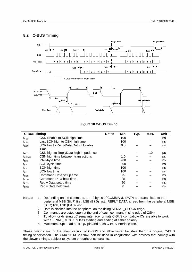
C4FM Data Modem CMX7031/CMX7041
© 2007 CML Microsystems Plc Page 49 D/7031/41_FI3.0/2
8.2 C-BUS Timing
Figure 18 C-BUS Timing
C-BUS Timing Notes Min. Typ. Max. Unit tCSE CSN Enable to SClk high time 100 – – ns tCSH Last SClk high to CSN high time 100 – – ns tLOZ SClk low to ReplyData Output Enable
Time 0.0 – – ns
tHIZ CSN high to ReplyData high impedance – – 1.0 µs tCSOFF CSN high time between transactions 1.0 – – µs tNXT Inter-byte time 200 – – ns tCK SClk cycle time 200 – – ns tCH SClk high time 100 – – ns tCL SClk low time 100 – – ns tCDS Command Data setup time 75 – – ns tCDH Command Data hold time 25 – – ns tRDS Reply Data setup time 50 – – ns tRDH Reply Data hold time 0 – – ns Notes: 1. Depending on the command, 1 or 2 bytes of COMMAND DATA are transmitted to the
peripheral MSB (Bit 7) first, LSB (Bit 0) last. REPLY DATA is read from the peripheral MSB (Bit 7) first, LSB (Bit 0) last.
2. Data is clocked into the peripheral on the rising SERIAL_CLOCK edge. 3. Commands are acted upon at the end of each command (rising edge of CSN). 4. To allow for differing µC serial interface formats C-BUS compatible ICs are able to work
with SERIAL_CLOCK pulses starting and ending at either polarity. 5. Maximum 30pF load on IRQN pin and each C-BUS interface line. These timings are for the latest version of C-BUS and allow faster transfers than the original C-BUS timing specification. The CMX7031/CMX7041 can be used in conjunction with devices that comply with the slower timings, subject to system throughput constraints.

C4FM Data Modem CMX7031/CMX7041
© 2007 CML Microsystems Plc Page 50 D/7031/41_FI3.0/2
8.3 Packaging
ABC
H
TYP. MAX.MIN.DIM.
J
PTY
1.000.80
0.05
0° 12°
0.30
0.50
0.00
0.20
0.18
9.00 BSC9.00 BSC
**
NOTE :
* All dimensions in mmAngles are in degrees
A & B are reference data and donot include mold deflash or protrusions.
F 7.957.00G 7.957.00G1 0.225
L 0.500.30M 0.75
Index Area 1
Dot
Index Area 2
Dot Chamfer
ExposedMetal Pad
Index Area 1 is located directly above Index Area 2
The underside of the package has an exposed metal pad which can be soldered to the pcb to enhance the thermal conductivityand mechanical strength of the package fixing. Where advised, an electrical connection to this metal pad may also be required
Figure 19 Mechanical outline for 64-pad VQFN (Q1)
Order as part no. CMX7031Q1
Figure 20 Mechanical outline for 64-pin LQFP (L9)
Order as part no. CMX7031L9

C4FM Data Modem CMX7031/CMX7041
© 2007 CML Microsystems Plc Page 51 D/7031/41_FI3.0/2
ABC
H
TYP. MAX.MIN.DIM.
J
PTY
1.000.80
0.05
0° 12°
0.30
0.50
0.00
0.20
0.18
7.00 BSC7.00 BSC
**
NOTE :
* All dimensions in mmAngles are in degrees
A & B are reference data and donot include mold deflash or protrusions.
F 5.252.75G 5.252.75G1 0.225
L 0.500.30M 0.75
Index Area 1
Dot
Index Area 2
Dot Chamfer
Index Area 1 is located directly above Index Area 2
ExposedMetal Pad
The underside of the package has an exposed metal pad which can be soldered to the pcb to enhance the thermal conductivityand mechanical strength of the package fixing. Where advised, an electrical connection to this metal pad may also be required
Figure 21 Mechanical Outline of 48-pin VQFN (Q3)
Order as part no. CMX7041Q3
Figure 22 Mechanical Outline of 48-pin LQFP (L4)
Order as part no. CMX7041L4

C4FM Data Modem CMX7031/CMX7041
© 2007 CML Microsystems Plc Page 52 D/7031/41_FI3.0/2
About FirmASIC®
CML’s proprietary FirmASIC® component technology reduces cost, time to market and development risk, with increased flexibility for the designer and end application. FirmASIC® combines Analogue, Digital, Firmware and Memory technologies in a single silicon platform that can be focused to deliver the right feature mix, performance and price for a target application family. Specific functions of a FirmASIC® device are determined by uploading its Function Image™ during device initialization. New Function Images™ may be later provided to supplement and enhance device functions, expanding or modifying end-product features without the need for expensive and time-consuming design changes. FirmASIC® devices provide significant time to market and commercial benefits over Custom ASIC, Structured ASIC, FPGA and DSP solutions. They may also be exclusively customised where security or intellectual property issues prevent the use of Application Specific Standard Products (ASSP’s).
Handling precautions: This product includes input protection, however, precautions should be taken to prevent device damage from electro-static discharge. CML does not assume any responsibility for the use of any circuitry described. No IPR or circuit patent licences are implied. CML reserves the right at any time without notice to change the said circuitry and this product specification. CML has a policy of testing every product shipped using calibrated test equipment to ensure compliance with this product specification. Specific testing of all circuit parameters is not necessarily performed.