compact models - jmbussat/physics290e/fall-2006/tcad_documentati… · level 6 mosfet model and...
TRANSCRIPT

Compact ModelsVersion Y-2006.06, June 2006

ii
Copyright Notice and Proprietary InformationCopyright © 2006 Synopsys, Inc. All rights reserved. This software and documentation contain confidential and proprietary information that is the property of Synopsys, Inc. The software and documentation are furnished under a license agreement and may be used or copied only in accordance with the terms of the license agreement. No part of the software and documentation may be reproduced, transmitted, or translated, in any form or by any means, electronic, mechanical, manual, optical, or otherwise, without prior written permission of Synopsys, Inc., or as expressly provided by the license agreement.
Right to Copy DocumentationThe license agreement with Synopsys permits licensee to make copies of the documentation for its internal use only. Each copy shall include all copyrights, trademarks, service marks, and proprietary rights notices, if any. Licensee must assign sequential numbers to all copies. These copies shall contain the following legend on the cover page:
“This document is duplicated with the permission of Synopsys, Inc., for the exclusive use of __________________________________________ and its employees. This is copy number __________.”
Destination Control StatementAll technical data contained in this publication is subject to the export control laws of the United States of America. Disclosure to nationals of other countries contrary to United States law is prohibited. It is the reader’s responsibility to determine the applicable regulations and to comply with them.
DisclaimerSYNOPSYS, INC., AND ITS LICENSORS MAKE NO WARRANTY OF ANY KIND, EXPRESS OR IMPLIED, WITH REGARD TO THIS MATERIAL, INCLUDING, BUT NOT LIMITED TO, THE IMPLIED WARRANTIES OF MERCHANTABILITY AND FITNESS FOR A PARTICULAR PURPOSE.
Registered Trademarks (®)Synopsys, AMPS, Arcadia, C Level Design, C2HDL, C2V, C2VHDL, Cadabra, Calaveras Algorithm, CATS, CRITIC, CSim, Design Compiler, DesignPower, DesignWare, EPIC, Formality, HSIM, HSPICE, Hypermodel, iN-Phase, in-Sync, Leda, MAST, Meta, Meta-Software, ModelTools, NanoSim, OpenVera, PathMill, Photolynx, Physical Compiler, PowerMill, PrimeTime, RailMill, RapidScript, Saber, SiVL, SNUG, SolvNet, Superlog, System Compiler, TetraMAX, TimeMill, TMA, VCS, Vera, and Virtual Stepper are registered trademarks of Synopsys, Inc.
Trademarks (™)Active Parasitics, AFGen, Apollo, Apollo II, Apollo-DPII, Apollo-GA, ApolloGAII, Astro, Astro-Rail, Astro-Xtalk, Aurora, AvanTestchip, AvanWaves, BCView, Behavioral Compiler, BOA, BRT, Cedar, ChipPlanner, Circuit Analysis, Columbia, Columbia-CE, Comet 3D, Cosmos, CosmosEnterprise, CosmosLE, CosmosScope, CosmosSE, Cyclelink, Davinci, DC Expert, DC Professional, DC Ultra, DC Ultra Plus, Design Advisor, Design Analyzer, Design Vision, DesignerHDL, DesignTime, DFM-Workbench, Direct RTL, Direct Silicon Access, Discovery, DW8051, DWPCI, Dynamic-Macromodeling, Dynamic Model Switcher, ECL Compiler, ECO Compiler, EDAnavigator, Encore, Encore PQ, Evaccess, ExpressModel, Floorplan Manager, Formal Model Checker, FoundryModel, FPGA Compiler II, FPGA Express, Frame Compiler, Galaxy, Gatran, HANEX, HDL Advisor, HDL Compiler, Hercules, Hercules-Explorer, Hercules-II, Hierarchical Optimization Technology, High Performance Option, HotPlace, HSIMplus, HSPICE-Link, iN-Tandem, Integrator, Interactive Waveform Viewer, i-Virtual Stepper, Jupiter, Jupiter-DP, JupiterXT, JupiterXT-ASIC, JVXtreme, Liberty, Libra-Passport, Library Compiler, Libra-Visa, Magellan, Mars, Mars-Rail, Mars-Xtalk, Medici, Metacapture, Metacircuit, Metamanager, Metamixsim, Milkyway, ModelSource, Module Compiler, MS-3200, MS-3400, Nova Product Family, Nova-ExploreRTL, Nova-Trans, Nova-VeriLint, Nova-VHDLlint, Optimum Silicon, Orion_ec, Parasitic View, Passport, Planet, Planet-PL, Planet-RTL, Polaris, Polaris-CBS, Polaris-MT, Power Compiler, PowerCODE, PowerGate, ProFPGA, ProGen, Prospector, Protocol Compiler, PSMGen, Raphael, Raphael-NES, RoadRunner, RTL Analyzer, Saturn, ScanBand, Schematic Compiler, Scirocco, Scirocco-i, Shadow Debugger, Silicon Blueprint, Silicon Early Access, SinglePass-SoC, Smart Extraction, SmartLicense, SmartModel Library, Softwire, Source-Level Design, Star, Star-DC, Star-MS, Star-MTB, Star-Power, Star-Rail, Star-RC, Star-RCXT, Star-Sim, Star-SimXT, Star-Time, Star-XP, SWIFT, Taurus, TimeSlice, TimeTracker, Timing Annotator, TopoPlace, TopoRoute, Trace-On-Demand, True-Hspice, TSUPREM-4, TymeWare, VCS Express, VCSi, Venus, Verification Portal, VFormal, VHDL Compiler, VHDL System Simulator, VirSim, and VMC are trademarks of Synopsys, Inc.
Service Marks (SM)MAP-in, SVP Café, and TAP-in are service marks of Synopsys, Inc.
SystemC is a trademark of the Open SystemC Initiative and is used under license.ARM and AMBA are registered trademarks of ARM Limited.All other product or company names may be trademarks of their respective owners.
Compact Models, Y-2006.06

COMPACT MODELS CONTENTS
Compact ModelsAbout this manual ...............................................................................................................................vii
Audience ............................................................................................................................................................ viiRelated publications........................................................................................................................................... viiTypographic conventions .................................................................................................................................. viiiCustomer support.............................................................................................................................................. viiiAcknowledgments ............................................................................................................................................... ix
Chapter 1 SPICE models ......................................................................................................................1Overview ..............................................................................................................................................................1
Temperature dependencies ...........................................................................................................................3Elementary devices..............................................................................................................................................3
Simple linear resistor......................................................................................................................................3Capacitor ........................................................................................................................................................4Inductor ..........................................................................................................................................................5Coupled (mutual) inductors ............................................................................................................................5Voltage-controlled switch ...............................................................................................................................6Current-controlled switch................................................................................................................................7
Voltage and current sources ................................................................................................................................8Values of independent sources ......................................................................................................................8
DC source ...............................................................................................................................................8Pulse source ...........................................................................................................................................8Sinusoidal source....................................................................................................................................9Exponential source................................................................................................................................10Piecewise linear source ........................................................................................................................11Single-frequency FM source .................................................................................................................12
Independent voltage source .........................................................................................................................13Independent current source .........................................................................................................................14Voltage-controlled current source ................................................................................................................15Voltage-controlled voltage source ................................................................................................................15Current-controlled current source.................................................................................................................16Current-controlled voltage source ................................................................................................................16
Transistors and diodes.......................................................................................................................................17Junction diode ..............................................................................................................................................17Bipolar junction transistor (BJT) ...................................................................................................................18Junction field effect transistor (JFET)...........................................................................................................21MOSFET models (NMOS and PMOS) .........................................................................................................23Level 1 MOSFET model and Meyer capacitance model ..............................................................................24Level 2 MOSFET model and Meyer capacitance model ..............................................................................26Level 3 MOSFET model and Meyer capacitance model ..............................................................................29Level 6 MOSFET model and Meyer capacitance model ..............................................................................31Berkeley short-channel IGFET model (BSIM1) ............................................................................................34Berkeley short-channel IGFET model (BSIM2) ............................................................................................38Berkeley short-channel IGFET model version 3 (BSIM3) ............................................................................44Berkeley short-channel IGFET model version 4 (BSIM4) ............................................................................59BSIMPD2.2 MOSFET model........................................................................................................................83GaAs MESFET model ................................................................................................................................103
Chapter 2 HSPICE models................................................................................................................105Overview ..........................................................................................................................................................105Level 1 IDS: Schichman–Hodges model..........................................................................................................105Level 2 IDS: Grove–Frohman model................................................................................................................106Level 3 IDS: Empirical model ...........................................................................................................................106
iii

COMPACT MODELSCONTENTS
Level 28 modified BSIM model ........................................................................................................................106Level 49 BSIM3v3 MOS model ........................................................................................................................106Level 53 BSIM3v3 MOS model ........................................................................................................................107Level 54 BSIM4.0 model ..................................................................................................................................107Level 57 UC Berkeley BSIM3-SOI model ........................................................................................................107Level 59 UC Berkeley BSIM3-SOI FD model...................................................................................................107
Chapter 3 Built-in models.................................................................................................................109Overview ..........................................................................................................................................................109Parameter interface..........................................................................................................................................109Electrothermal resistor .....................................................................................................................................110
Chapter 4 Compact model interface in Sentaurus Device ............................................................113Overview ..........................................................................................................................................................113Model equations...............................................................................................................................................113
Example: Coupled inductance....................................................................................................................116State variables and parameters .................................................................................................................117Plotting during transient simulations...........................................................................................................117
Hierarchical description of compact models.....................................................................................................118Electrothermal models .....................................................................................................................................119Data structures of Sentaurus Device ...............................................................................................................120Interface subroutines........................................................................................................................................120
cmi_device_create .....................................................................................................................................121cmi_device_set_param ..............................................................................................................................121cmi_device_initialize...................................................................................................................................121cmi_device_get_param ..............................................................................................................................121cmi_device_delete......................................................................................................................................121cmi_pset_create .........................................................................................................................................122cmi_pset_set_param ..................................................................................................................................122cmi_pset_initialize ......................................................................................................................................122cmi_pset_get_param..................................................................................................................................122cmi_pset_delete .........................................................................................................................................122cmi_instance_create ..................................................................................................................................123cmi_instance_set_param ...........................................................................................................................123cmi_instance_initialize................................................................................................................................123cmi_instance_get_param ...........................................................................................................................123cmi_instance_get_rhs ................................................................................................................................123cmi_instance_get_jacobian ........................................................................................................................124cmi_instance_is_physical...........................................................................................................................124cmi_instance_delete...................................................................................................................................124
Run-time support..............................................................................................................................................125cmi_starttime ..............................................................................................................................................125cmi_stoptime ..............................................................................................................................................125cmi_min_timestep ......................................................................................................................................125cmi_max_timestep .....................................................................................................................................125cmi_set_event ............................................................................................................................................125cmi_set_max_timestep...............................................................................................................................126
Compilation ......................................................................................................................................................126Command file of Sentaurus Device..................................................................................................................127Summary..........................................................................................................................................................127Syntax of compact circuit files..........................................................................................................................128
iv
COMPACT MODELS CONTENTS
Header files ......................................................................................................................................................132CCMBaseParam.h .....................................................................................................................................132CCMBaseDevice.h .....................................................................................................................................134CCMBasePSet.h ........................................................................................................................................135CCMBaseInstance.h ..................................................................................................................................136CMIModels.h ..............................................................................................................................................137CMISupport.h .............................................................................................................................................139
Coupled inductances........................................................................................................................................139coupled.ccf .................................................................................................................................................139coupled.C ...................................................................................................................................................140
Electrothermal resistance.................................................................................................................................144tres.ccf........................................................................................................................................................145tres.C..........................................................................................................................................................146
Bibliography ......................................................................................................................................151
v

COMPACT MODELSCONTENTS
vi
COMPACT MODELS ABOUT THIS MANUAL
Compact Models
About this manual
This manual is to be used in conjunction with the Sentaurus Device User Guide. It provides details aboutthe four types of compact model that are available in Sentaurus Device:
The SPICE models used in Sentaurus Device are based on the Berkeley SPICE model version 3F5[2][3][4][5]. The BSIM3v3.2, BSIM4.1.0, and BSIMPD2.2 MOS models are also available.
Several frequently used HSPICE models are available.
The built-in models work in a similar way to the SPICE models. However, they provide additionalfunctionality not found in the SPICE models.
User-defined models can be implemented in Sentaurus Device by using a compact model interface(CMI). The model code must be implemented in C++ and it is linked to Sentaurus Devicedynamically at run-time. No access to the source code of Sentaurus Device is necessary. The speedof user-defined models is comparable to that of built-in models in Sentaurus Device.
The main chapters are:
Chapter 1 describes the SPICE models available in Sentaurus Device.
Chapter 2 describes the HSPICE models available in Sentaurus Device.
Chapter 3 describes the built-in models available in Sentaurus Device.
Chapter 4 describes the compact model interface for user-defined models.
AudienceThis manual is intended for users of the Sentaurus Device software package.
Related publicationsFor additional information about Compact Models, see:
The Compact Models release notes, available on SolvNet (see Accessing SolvNet on page viii).
Documentation on the Web, which is available through SolvNet athttps://solvnet.synopsys.com/DocsOnWeb.
Synopsys Online Documentation (SOLD), which is included with the software for CD users or isavailable to download through the Synopsys Electronic Software Transfer (EST) system.
vii

COMPACT MODELSABOUT THIS MANUAL
Typographic conventions
Customer supportCustomer support is available through SolvNet online customer support and through contacting theSynopsys Technical Support Center.
Accessing SolvNet
SolvNet includes an electronic knowledge base of technical articles and answers to frequently askedquestions about Synopsys tools. SolvNet also gives you access to a wide range of Synopsys onlineservices including software downloads, documentation on the Web, and “Enter a Call to the SupportCenter.”
To access SolvNet:
1. Go to the SolvNet Web page at http://solvnet.synopsys.com.
2. If prompted, enter your user name and password. (If you do not have a Synopsys user name andpassword, follow the instructions to register with SolvNet.)
If you need help using SolvNet, click HELP in the top-right menu bar or in the footer.
Convention Explanation
Blue text Identifies a cross-reference (only on the screen).
Bold text Identifies a selectable icon, button, menu, or tab. It also indicates the name of a field, window, dialog box, or panel.
Courier font Identifies text that is displayed on the screen or that the user must type. It identifies the names of files, directories, paths, parameters, keywords, and variables.
Italicized text Used for emphasis, the titles of books and journals, and non-English words. It also identifies components of an equation or a formula, a placeholder, or an identifier.
NOTE Identifies important information.
viii

COMPACT MODELS ABOUT THIS MANUAL
Contacting the Synopsys Technical Support Center
If you have problems, questions, or suggestions, you can contact the Synopsys Technical Support Centerin the following ways:
Open a call to your local support center from the Web by going to http://solvnet.synopsys.com(Synopsys user name and password required), then clicking “Enter a Call to the Support Center.”
Send an e-mail message to your local support center:
• E-mail [email protected] from within North America.
• Find other local support center e-mail addresses at http://www.synopsys.com/support/support_ctr.
Telephone your local support center:
• Call (800) 245-8005 from within the continental United States.
• Call (650) 584-4200 from Canada.
• Find other local support center telephone numbers at http://www.synopsys.com/support/support_ctr.
Contacting your local TCAD Support Team directly
Send an e-mail message to:
[email protected] from within North America and South America.
[email protected] from within Europe.
[email protected] from within Asia Pacific (China, Taiwan, Singapore, Malaysia,India, Australia).
[email protected] from Korea.
[email protected] from Japan.
AcknowledgmentsThe SPICE circuit simulator was developed by the Department of Electrical Engineering and ComputerScience (EECS), University of California, Berkeley, and is copyrighted by the University of California.
BSIM3 was developed by the Device Research Group of the Department of Electrical Engineering andComputer Science (EECS), University of California, Berkeley, and is copyrighted by the University ofCalifornia (http://www-device.eecs.berkeley.edu/~bsim3).
ix

COMPACT MODELSABOUT THIS MANUAL
x

COMPACT MODELS CHAPTER 1 SPICE MODELS
Compact Models
CHAPTER 1 SPICE models
This chapter describes the SPICE models available in Sentaurus Device.
OverviewThe following SPICE models are available in Sentaurus Device:
Elementary devices (see Elementary devices on page 3)
Voltage and current sources (see Voltage and current sources on page 8)
Transistors and diodes (see Transistors and diodes on page 17)
NOTE The compact model for an arbitrary source (ASRC) and the models for transmission lines(LTRA, Tranline, URC) are not available in Sentaurus Device.
The model for a bipolar junction transistor (BJT) is based on the integral charge model of Gummel andPoon. However, if the Gummel–Poon parameters are not specified, the model reduces to the simplerEbers–Moll model. In either case, charge–storage effects, Ohmic resistances, and a current-dependentoutput conductance can be included. The diode model can be used for either junction diodes or Schottkybarrier diodes. The junction field effect transistor (JFET) model is based on the FET model of Shichmanand Hodges.
Several MOSFET models are implemented: Mos1 is described by a square-law I–V characteristic;Mos2 [6] is an analytic model; Mos3 [6] is a semi-empirical model; Mos6 [7] is a simple analytic modelaccurate in the short-channel region; and BSIM1 [8][9][10] and BSIM2 [11] are the Berkeley short-channel IGFET models. Mos2, Mos3, and BSIM1 include second-order effects such as channel-lengthmodulation, subthreshold conduction, scattering-limited velocity saturation, small-size effects, andcharge-controlled capacitances.
BSIM3 is a physics-based, accurate, scalable, robust and predictive MOSFET SPICE model [1]. Sincethe third iteration of BSIM3, BSIM3 Version 3 (commonly abbreviated to BSIM3v3), was establishedby SEMATECH as the first industrywide standard of its kind, BSIM3v3 is widely used by mostsemiconductor and integrated circuit (IC) design companies worldwide for device modeling and CMOSIC design.
1
COMPACT MODELSCHAPTER 1 SPICE MODELS
BSIM3 includes compact, analytic expressions for the following physical phenomena:
Short-channel and narrow-channel effects on threshold voltage
Nonuniform doping effect (in both lateral and vertical directions)
Mobility reduction due to vertical field
Bulk charge effect
Carrier velocity saturation
Drain-induced barrier lowering (DIBL)
Channel-length modulation (CLM)
Substrate current-induced body effect (SCBE)
Subthreshold conduction
Source and drain parasitic resistances
BSIM3 has extensive built-in dependencies of important dimensional and processing parameters (forexample, channel length, width, gate oxide thickness, and substrate doping concentration). Thesedependencies allow users to model the MOSFET accurately over a wide range of channel lengths andchannel widths for present and future technologies.
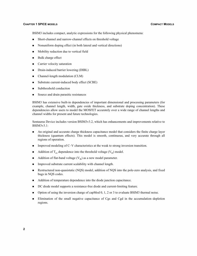
Sentaurus Device includes version BSIM3v3.2, which has enhancements and improvements relative toBSIM3v3.1:
An original and accurate charge thickness capacitance model that considers the finite charge layerthickness (quantum effects). This model is smooth, continuous, and very accurate through allregions of operation.
Improved modeling of C–V characteristics at the weak to strong inversion transition.
Addition of Tox dependence into the threshold voltage (Vth) model.
Addition of flat-band voltage (Vfb) as a new model parameter.
Improved substrate current scalability with channel length.
Restructured non-quasistatic (NQS) model, addition of NQS into the pole-zero analysis, and fixedbugs in NQS codes.
Addition of temperature dependence into the diode junction capacitance.
DC diode model supports a resistance-free diode and current-limiting feature.
Option of using the inversion charge of capMod 0, 1, 2 or 3 to evaluate BSIM3 thermal noise.
Elimination of the small negative capacitance of Cgs and Cgd in the accumulation–depletionregions.
2

COMPACT MODELS CHAPTER 1 SPICE MODELS
A separate set of channel-width and channel-length dependence parameters (llc, lwc, lwlc, wlc, wwc,and wwlc) to calculate Weff and Leff for the C–V model for a better fit of the capacitance data.
Addition of parameter checking to avoid bad values for certain parameters.
BSIM4 is the latest MOSFET SPICE model from Berkeley.
Temperature dependenciesThe SPICE models assume that input data has been measured at a nominal temperature of 27oC. Thisvalue can be overridden for the parameter sets that provide a tnom parameter.
Similarly, the default operating temperature of all SPICE instances is 27oC (300.15 K). This default canbe changed for those instances that provide a temp parameter.
For details of the BSIM temperature adjustments, refer to the literature [12][13].
Elementary devices
Simple linear resistorResistors are specified by giving the value of the resistance [ ]. This value can be positive or negative,but not zero.
A more general form of the resistor allows for the modeling of temperature effects and the calculationof the actual resistance value from strictly geometric information and specifications of the process. Thesheet resistance is used, with the narrowing parameter and the length and width of the device, todetermine the nominal resistance by the formula:
(1)
defw is used to supply a default value for if none is specified for the device. If either or is notspecified, the standard default resistance 1 k is used. After the nominal resistance is calculated, it isadjusted for temperature by the formula:
(2)
Device name: Resistor
Default parameter set name: Resistor_pset
Electrodes: R+, R-Internal variables: None
Ω
r rsh l narrow–w narrow–-----------------------------=
w rsh lΩ
r temp( ) r tnom( ) 1 tc1 temp tnom–( )⋅+( )⋅ tc2 temp tnom–( )2 )⋅+=
3

COMPACT MODELSCHAPTER 1 SPICE MODELS
CapacitorIf the value of capacitance is not given, it can be computed from strictly geometric information and thespecifications of the process as follows:
(3)
Table 1 Resistor model parameters
Name Description Type Default Unit
defw Default device width double 1e-05 m
narrow Narrowing of resistor double 0 m
rsh Sheet resistance double 0 /sq
tc1 First-order temperature coefficient double 0 oC–1
tc2 Second-order temperature coefficient double 0 oC–2
tnom Parameter measurement temperature double 27 oC
Table 2 Resistor instance parameters
Name Description Type Default Unit
resistance Resistance double 1000
temp Instance operating temperature double 27 oC
l Length double 0 m
w Width double 1e-05 m
Device name: Capacitor
Default parameter set name: Capacitor_pset
Electrodes: C+, C-Internal variables: None
Table 3 Capacitor model parameters
Name Description Type Default Unit
cj Bottom capacitance per area double 0 F/m2
cjsw Sidewall capacitance per meter double 0 F/m
defw Default width double 1e-05 m
narrow Width correction factor double 0 m
Ω
Ω
capacitance cj l narrow–( ) w narrow–( )⋅ ⋅ 2 cjsw l w 2 narrow⋅–+( )⋅ ⋅+=
4
COMPACT MODELS CHAPTER 1 SPICE MODELS
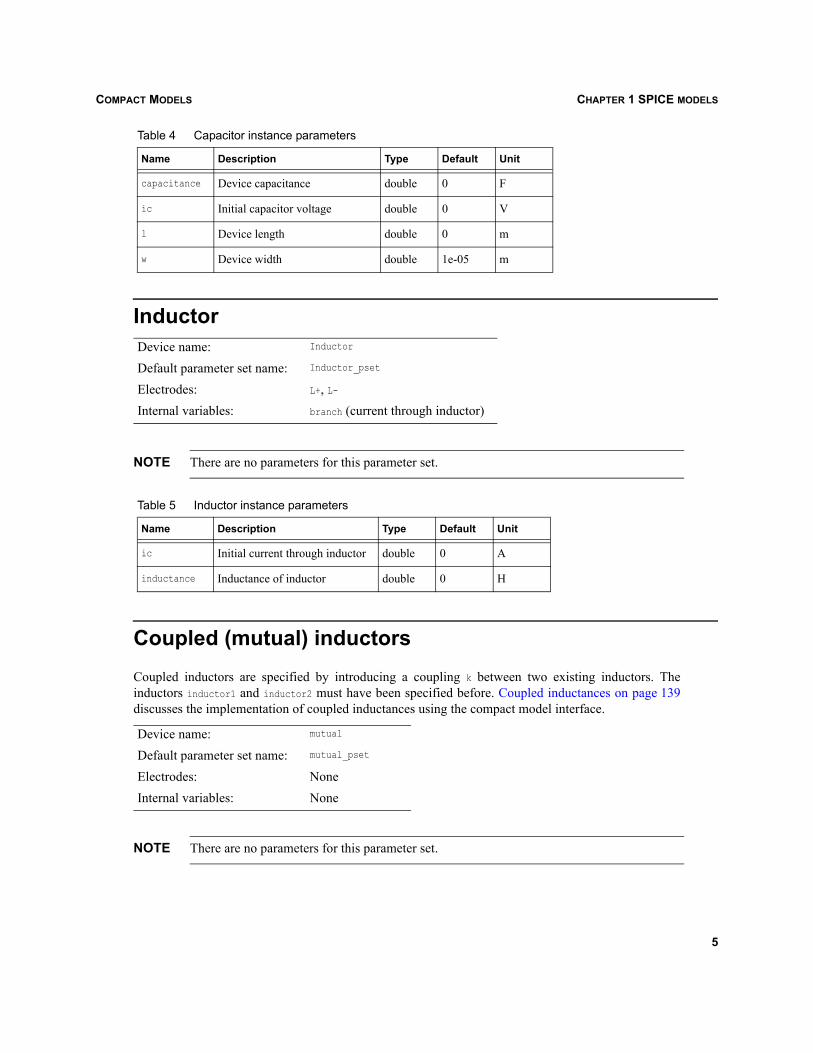
Inductor
NOTE There are no parameters for this parameter set.
Coupled (mutual) inductorsCoupled inductors are specified by introducing a coupling k between two existing inductors. Theinductors inductor1 and inductor2 must have been specified before. Coupled inductances on page 139discusses the implementation of coupled inductances using the compact model interface.
NOTE There are no parameters for this parameter set.
Table 4 Capacitor instance parameters
Name Description Type Default Unit
capacitance Device capacitance double 0 F
ic Initial capacitor voltage double 0 V
l Device length double 0 m
w Device width double 1e-05 m
Device name: Inductor
Default parameter set name: Inductor_pset
Electrodes: L+, L-Internal variables: branch (current through inductor)
Table 5 Inductor instance parameters
Name Description Type Default Unit
ic Initial current through inductor double 0 A
inductance Inductance of inductor double 0 H
Device name: mutual
Default parameter set name: mutual_pset
Electrodes: NoneInternal variables: None
5

COMPACT MODELSCHAPTER 1 SPICE MODELS
Voltage-controlled switchThe electrodes S+ and S- are the nodes between which the switch terminals are connected. The electrodesSC+ and SC- are the positive and negative controlling nodes, respectively. The switch is not ideal becauseit must have a finite positive resistance in the off state. However, the value can be chosen such that it iseffectively infinite compared to the other circuit elements.
The switch is switched on if the controlling voltage is greater than vt + vh. It is switched off if thecontrolling voltage is smaller than vt - vh.
Table 6 Coupled inductors instance parameters
Name Description Type Default Unit
coefficient (redundant parameter) double 0 –
inductor1 First coupled inductor string “ ” –
inductor2 Second coupled inductor string “ ” –
k Mutual inductance double 0 –
Device name: Switch
Default parameter set name: Switch_pset
Electrodes: S+, S-, SC+, SC-Internal variables: None
Table 7 Voltage-controlled switch model parameters
Name Description Type Default Unit
roff Resistance when open double 1e+12
ron Resistance when closed double 1
vh Hysteresis voltage double 0 V
vt Threshold voltage double 0 V
Table 8 Voltage-controlled switch instance parameters
Name Description Type Default Unit
off Switch initially open integer – –
on Switch initially closed integer – –
Ω
Ω
6

COMPACT MODELS CHAPTER 1 SPICE MODELS
Current-controlled switchThe electrodes W+ and W- are the nodes between which the switch terminals are connected. The switch iscontrolled by the current that flows through the voltage source given by the parameter control. Thedirection of positive controlling current flow is from the positive node, through the source, to thenegative node.
NOTE This voltage source must be specified before the switch.
The switch is not ideal because it must have a finite positive resistance in the off state. However, thevalue can always be chosen such that it is effectively infinite compared to the other circuit elements. Theswitch is switched on if the controlling current is greater than it + ih. It is switched off if the controllingcurrent is smaller than it – ih.
Device name: CSwitch
Default parameter set name: CSwitch_pset
Electrodes: W+, W-Internal variables: None
Table 9 Current-controlled switch model parameters
Name Description Type Default Unit
ih Hysteresis current double 0 A
it Threshold current double 0 A
roff Open resistance double 1e+12
ron Closed resistance double 1
Table 10 Current-controlled switch instance parameters
Name Description Type Default Unit
control Name of controlling source string “ ” –
off Initially open integer – –
on Initially closed integer – –
Ω
Ω
7

COMPACT MODELSCHAPTER 1 SPICE MODELS
Voltage and current sources
Values of independent sourcesThe independent voltage and current sources have the same parameters.
DC source
The parameter dc specifies the DC value of the source. For example, the parameter dc = 10 defines a DCvoltage/current source of 10 V/10 A.
Pulse source
The pulse parameter must be a vector of length 7. Its entries define a transient pulse as shown in Table 11.
Such a pulse produces the values in Table 12.
Table 11 Pulse source instance parameters
Parameter Meaning Unit
v1 = pulse [0] Initial value V or A
v2 = pulse [1] Pulsed value V or A
td = pulse [2] Delay time s
tr = pulse [3] Rise time s
tf = pulse [4] Fall time s
pw = pulse [5] Pulse width s
per = pulse [6] Period s
Table 12 Pulse source values
Time Value Time Value
0 v1 td+tr+pw+tf v1
td v1 per+td v1
td+tr v2 per+td+tr v2
td+tr+pw v2
8

COMPACT MODELS CHAPTER 1 SPICE MODELS
Intermediate values are determined by linear interpolation. For example, the specification:
pulse = (-0.2 1 0.8 0.2 2.0 1 5)
produces the pulse shown in Figure 1.
Figure 1 Pulse source
Sinusoidal source
The sine parameter must be a vector of length 5. Its entries are listed in Table 13.
A sinusoidal source produces the values shown in Table 14.
Table 13 Sinusoidal source instance parameters
Parameter Meaning Unit
vo = sine [0] Offset V or A
va = sine [1] Amplitude V or A
freq = sine [2] Frequency Hz
td = sine [3] Delay s
theta = sine [4] Damping factor s–1
Table 14 Sinusoidal source values
Time Value
0 10 15 20
0
0.5
1
5
t td≤ vo
t td> vo va e t td–( ) theta⋅– 2 π freq t td–( )⋅ ⋅ ⋅( )sin⋅ ⋅+
9

COMPACT MODELSCHAPTER 1 SPICE MODELS
For example, the specification:
sine = (0.2 0.4 0.25 4 0.01)
produces the sine wave shown in Figure 2.
Figure 2 Sine source
Exponential source
The exp parameter must be a vector of length 6 with the entries as presented in Table 15.
Table 15 Exponential source instance parameters
Parameter Meaning Unit
v1 = exp [0] Initial value V or A
v2 = exp [1] Pulsed value V or A
td1 = exp [2] Rise delay time s
tau1 = exp [3] Rise time constant s
td2 = exp [4] Fall delay time s
tau2 = exp [5] Fall time constant s
0 10 15 20-0.2
0
0.2
0.4
0.6
5
10

COMPACT MODELS CHAPTER 1 SPICE MODELS
The shape of the waveform is described by Table 16.
For example, the specification:
exp = (0.2 0.4 2 5 10 3)
produces the shark fin shown in Figure 3.
Figure 3 Exponential source
Piecewise linear source
The parameter pwl must be a vector of even size. It consists of pairs that specify the value [Vor A] at the time . The value of the source at intermediate values of time is determined by usinglinear interpolation on the input values.
Table 16 Exponential source values
Time Value
t td1≤ v1
td1 t< td2≤ v1 v2 v1–( ) 1 et td1–tau1
----------------––
⎝ ⎠⎜ ⎟⎛ ⎞
+
t td2> v1 v2 v1–( ) 1 et td1–tau1
----------------––
⎝ ⎠⎜ ⎟⎛ ⎞
v1 v2–( ) 1 et td2–tau2
----------------––
⎝ ⎠⎜ ⎟⎛ ⎞
+ +
0 10 15 20
0.2
0.25
0.3
0.35
5
tk vk,( ) vkt tk=
11

COMPACT MODELSCHAPTER 1 SPICE MODELS
For example, the specification:
pwl = (0 0 2 2 3 -1 6 6 10 5 12 -1 16 4 19 2 20 5)
produces the curve shown in Figure 4.
Figure 4 Piecewise linear source
Single-frequency FM source
The parameter sffm must be a vector of size 5. Its entries are explained in Table 17.
The shape of the waveform is described by:
(4)
Table 17 Single-frequency FM source instance parameters
Parameter Description Unit
vo = sffm [0] Offset V or A
va = sffm [1] Amplitude V or A
fc = sffm [2] Carrier frequency Hz
mdi = sffm [3] Modulation index –
fs = sffm [4] Signal frequency Hz
0 10 15 20
0
2
4
6
5
v t( ) vo va 2 π fc t mdi 2 π fs t⋅ ⋅ ⋅( )sin⋅+⋅ ⋅ ⋅( )sin⋅+=
12

COMPACT MODELS CHAPTER 1 SPICE MODELS
For example, the specification:
sffm = (1 2 1 3 0.25)
produces the signal shown in Figure 5.
Figure 5 Single-frequency FM source
Independent voltage sourceA SPICE voltage source can be used as an ‘ammeter’ in a circuit, that is, a zero-valued voltage sourcecan be inserted into the circuit to measure the current. Voltage sources are referenced by the controlparameter in current-controlled current sources (CCCS), current-controlled voltage sources (CCVS),and current-controlled switches (CSwitch).
Only one of the parameters dc, pulse, sine or sin, exp, pwl, or sffm must be specified. For DC simulations,the value of the source for the time t = 0 is used.
NOTE There are no parameters for this parameter set.
Device name: Vsource
Default parameter set name: Vsource_pset
Electrodes: V+, V-Internal variables: branch (current through voltage source)
0 10 15 20
-1
0
1
2
3
5
13
COMPACT MODELSCHAPTER 1 SPICE MODELS
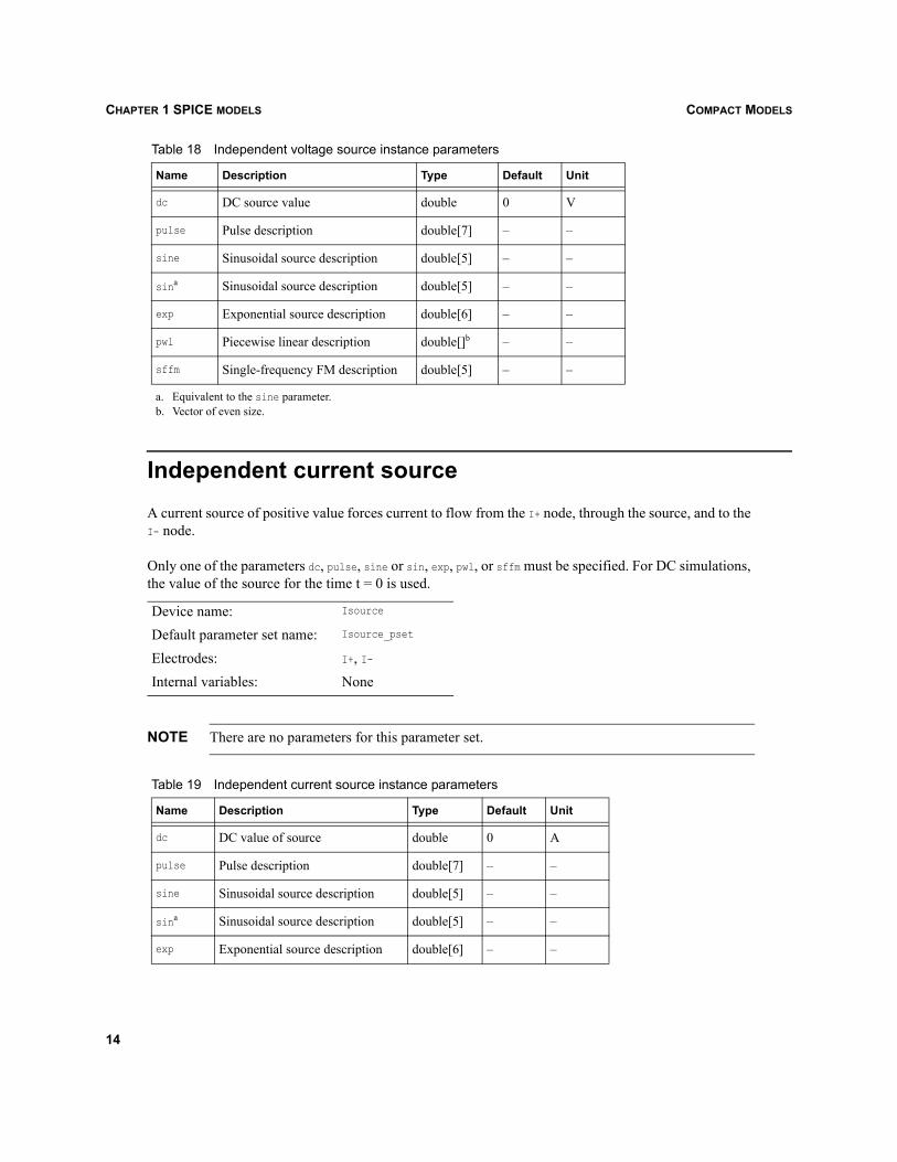
Independent current sourceA current source of positive value forces current to flow from the I+ node, through the source, and to theI- node.
Only one of the parameters dc, pulse, sine or sin, exp, pwl, or sffm must be specified. For DC simulations,the value of the source for the time t = 0 is used.
NOTE There are no parameters for this parameter set.
Table 18 Independent voltage source instance parameters
Name Description Type Default Unit
dc DC source value double 0 V
pulse Pulse description double[7] – –
sine Sinusoidal source description double[5] – –
sina Sinusoidal source description double[5] – –
exp Exponential source description double[6] – –
pwl Piecewise linear description double[]b – –
sffm Single-frequency FM description double[5] – –
a. Equivalent to the sine parameter.b. Vector of even size.
Device name: Isource
Default parameter set name: Isource_pset
Electrodes: I+, I-Internal variables: None
Table 19 Independent current source instance parameters
Name Description Type Default Unit
dc DC value of source double 0 A
pulse Pulse description double[7] – –
sine Sinusoidal source description double[5] – –
sina Sinusoidal source description double[5] – –
exp Exponential source description double[6] – –
14

COMPACT MODELS CHAPTER 1 SPICE MODELS
Voltage-controlled current sourceV+ and V- are the positive and negative nodes, respectively. Current flows from the positive node, throughthe source, to the negative node. VC+ and VC- are the positive and negative controlling nodes, respectively.The value of the current is given by:
(5)
NOTE There are no parameters for this parameter set.
Voltage-controlled voltage sourceThe positive and negative nodes are V+ and V-, respectively. The positive and negative controlling nodesare VC+ and VC-, respectively. The value of the voltage is given by:
(6)
pwl Piecewise linear description double[]b – –
sffm Single-frequency FM description double[5] – –
a. Equivalent to the sine parameter.b. Vector of even size.
Device name: VCCS
Default parameter set name: VCCS_pset
Electrodes: V+, V-, VC+, VC-Internal variables: None
Table 20 Voltage-controlled current source instance parameter
Name Description Type Default Unit
gain Transconductance of source (gain) double 0
Device name: VCVS
Default parameter set name: VCVS_pset
Electrodes: V+, V-, VC+, VC-Internal variables: branch (current through voltage source)
Table 19 Independent current source instance parameters
Name Description Type Default Unit
i gain v VC+( ) v VC-( )–( )⋅=
Ω 1–
v gain v VC+( ) v VC-( )–( )⋅=
15

COMPACT MODELSCHAPTER 1 SPICE MODELS
NOTE There are no parameters for this parameter set.
Current-controlled current sourceThe positive and negative nodes are F+ and F-, respectively. Current flows from the positive node,through the source, to the negative node. The parameter control identifies the controlling voltage source,which must have been declared before. The direction of positive controlling current flow is from thepositive node, through the voltage source control, to the negative node. The value of the current is givenby:
(7)
NOTE There are no parameters for this parameter set.
Current-controlled voltage sourceH+ and H– are the positive and negative nodes, respectively. The parameter control identifies thecontrolling voltage source, which must have been declared before. The direction of positive controllingcurrent flow is from the positive node, through the voltage source control, to the negative node. Thevalue of the current is given by:
(8)
Table 21 Voltage-controlled voltage source instance parameter
Name Description Type Default Unit
gain Voltage gain double 0 –
Device name: CCCS
Default parameter set name: CCCS_pset
Electrodes: F+, F-Internal variables: None
Table 22 Current-controlled current source instance parameters
Name Description Type Default Unit
control Name of controlling source string “ ” –
gain Current gain double 0 –
i gain i control( )⋅=
v gain i control( )⋅=
16

COMPACT MODELS CHAPTER 1 SPICE MODELS
NOTE There are no parameters for this parameter set.
Transistors and diodes
Junction diodeThe DC characteristics of the diode are determined by the parameters is and n. An Ohmic resistance, rs,is included. Charge storage effects are modeled by a transit time, tt, and a nonlinear depletion layercapacitance, which is determined by the parameters cjo, vj, and m. The temperature dependence of thesaturation current is defined by the parameters eg (the energy) and xti (the saturation current temperatureexponent). The nominal temperature at which these parameters were measured is tnom. Reversebreakdown is modeled by an exponential increase in the reverse diode current and is determined by theparameters bv and ibv (both are positive numbers).
Device name: CCVS
Default parameter set name: CCVS_pset
Electrodes: H+, H-Internal variables: branch (current through voltage source)
Table 23 Current-controlled voltage source instance parameters
Name Description Type Default Unit
control Controlling voltage source string “ ” –
gain Transresistance (gain) double 0
Device name: Diode
Default parameter set name: Diode_pset
Electrodes: D+, D-Internal variables: internal (internal anode voltage, only available if )
Table 24 Diode model parameters
Name Description Type Default Unit
af Flicker noise exponent double 1 –
bv Reverse breakdown voltage double V
cj0 (redundant parameter) double 0 –
cjo Junction capacitance double 0 F
Ω
rs 0≠
∞
17

COMPACT MODELSCHAPTER 1 SPICE MODELS
Bipolar junction transistor (BJT)The BJT model in SPICE is an adaptation of the integral charge control model of Gummel and Poon.This modified Gummel–Poon model extends the original model to include several effects at high biaslevels. The model automatically simplifies to the Ebers–Moll model when certain parameters are notspecified. The parameter names used in the modified Gummel–Poon model have been chosen becausethey are easily understood by the user and better reflect both physical and circuit design thinking.
The DC model is defined by the parameters is, bf, nf, ise, ikf, and ne, which determine the forwardcurrent gain characteristics; is, br, nr, isc, kr, and nc, which determine the reverse current gaincharacteristics; and vaf and var, which determine the output conductance for forward and reverseregions.
eg Activation energy double 1.11 eV
fc Forward bias junction fit parameter double 0.5 –
ibv Current at reverse breakdown voltage double 0.001 A
is Saturation current double 1e-14 A
kf Flicker noise coefficient double 0 –
m Grading coefficient double 0.5 –
n Emission coefficient double 1 –
rs Ohmic resistance double 0
tnom Parameter measurement temperature double 27 oC
tt Transit time double 0 s
vj Junction potential double 1 V
xti Saturation current temperature exponential double 3 –
Table 25 Diode instance parameters
Name Description Type Default Unit
area Area factor double 1 –
ic Initial device voltage double 0 V
off Initially off integer 0 –
temp Instance temperature double 27 oC
Table 24 Diode model parameters
Name Description Type Default Unit
Ω
18

COMPACT MODELS CHAPTER 1 SPICE MODELS
Three Ohmic resistances rb, rc, and re are included, where rb can be high current–dependent. Basecharge storage is modeled by forward and reverse transit times, tf and tr; the forward transit time tfbeing bias- dependent if required, and nonlinear depletion layer capacitances, which are determined bycje, vje, and mje for the base–emitter junction; cjc, vjc, and mjc for the base–collector junction; and cjs,vjs, and mjs for the collector–substrate junction.
The temperature dependence of the saturation current, is, is determined by the energy gap, eg, and thesaturation current temperature exponent, xti. Additionally, base current temperature dependence ismodeled by the beta temperature exponent xtb in the new model. The values specified are assumed tohave been measured at the temperature tnom. The temp value is the temperature at which the device willoperate.
An npn transistor is obtained by specifying npn=1. Conversely, a pnp transistor is obtained by specifyingpnp=1.
Device name: BJT
Default parameter set name: BJT_pset
Electrodes: collector, base, emitter, substrateInternal variables: collector (internal collector voltage, only available if )
base (internal base voltage, only available if )emitter (internal emitter voltage, only available if )
Table 26 BJT model parameters
Name Description Type Default Unit
npn npn-type device integer 1 –
pnp pnp-type device integer 0 –
is Saturation current double 1e-16 A
bf Ideal forward beta double 100 –
nf Forward emission coefficient double 1 –
vaf Forward Early voltage double V
va (redundant parameter) double V
ikf Forward beta roll-off corner current double A
ik (redundant parameter) double A
ise Base–emitter leakage saturation current double 0 A
ne Base–emitter leakage emission coefficient double 1.5 –
br Ideal reverse beta double 1 –
nr Reverse emission coefficient double 1 –
var Reverse Early voltage double V
rc 0≠rb 0≠
re 0≠
∞
∞
∞
∞
∞
19

COMPACT MODELSCHAPTER 1 SPICE MODELS
vb (redundant parameter) double V
ikr Reverse beta roll-off corner current double A
isc Base–collector leakage saturation current double 0 A
nc Base–collector leakage emission coefficient double 2 –
rb Zero bias base resistance double 0
irb Current for base resistance=(rb+rbm)/2 double A
rbm Minimum base resistance double 0
re Emitter resistance double 0
rc Collector resistance double 0
cje Zero bias base–emitter depletion capacitance double 0 F
vje Base–emitter built-in potential double 0.75 V
pe (redundant parameter) double 0.75 V
mje Base–emitter junction grading coefficient double 0.33 –
me (redundant parameter) double 0.33 –
tf Ideal forward transit time double 0 s
xtf Coefficient for bias dependence of tf double 0 –
vtf Voltage giving VBC dependence of tf double V
itf High-current dependence of tf double 0 A
ptf Excess phase double 0 degree
cjc Zero bias base–collector depletion capacitance double 0 F
vjc Base–collector built-in potential double 0.75 V
pc (redundant parameter) double 0.75 V
mjc Base–collector junction grading coefficient double 0.33 –
mc (redundant parameter) double 0.33 –
xcjc Fraction of base–collector cap. to internal base double 1 –
tr Ideal reverse transit time double 0 s
cjs Zero bias collector–source capacitance double 0 F
ccs (redundant parameter) double 0 F
vjs Substrate junction built-in potential double 0.75 V
Table 26 BJT model parameters
Name Description Type Default Unit
∞
∞
Ω
∞
Ω
Ω
Ω
∞
20

COMPACT MODELS CHAPTER 1 SPICE MODELS
Junction field effect transistor (JFET)The JFET model is derived from the FET model of Shichman and Hodges. The DC characteristics aredefined by the parameters:
vto and beta, which determine the variation of drain current with gate voltage.
lambda, which determines the output conductance.
is, which is the saturation current of the two gate junctions.
Two Ohmic resistances, rd and rs, are included. Charge storage is modeled by nonlinear depletion-layercapacitances for both gate junctions, which vary as the –1/2 power of junction voltage and are definedby the parameters cgs, cgd, and pb.
ps (redundant parameter) double 0.75 V
mjs Substrate junction grading coefficient double 0 –
ms (redundant parameter) double 0 –
xtb Forward and reverse beta temperature exponent double 0 –
eg Energy gap for IS temperature dependency double 1.11 eV
xti Temperature exponent for IS double 3 –
fc Forward bias junction fit parameter double 0.5 –
tnom Parameter measurement temperature double 27 oC
kf Flicker noise coefficient double 0 –
af Flicker noise exponent double 1 –
Table 27 BJT instance parameters
Name Description Type Default Unit
area Area factor double 1 –
ic Initial condition vector double[2] – V
icvbe Initial base–emitter voltage double 0 V
icvce Initial collector–emitter voltage double 0 V
off Device initially off integer 0 –
temp Instance temperature double 27 oC
Table 26 BJT model parameters
Name Description Type Default Unit
21

COMPACT MODELSCHAPTER 1 SPICE MODELS
The temp value is the temperature at which the device will operate. A fitting parameter b is alsoavailable [14].
The type of the transistor must be specified by setting either njf=1 or pjf=1.
Device name: JFET
Default parameter set name: JFET_pset
Electrodes: Drain, Gate, SourceInternal variables: source (internal source voltage, only available if )
drain (internal drain voltage, only available if )
Table 28 JFET model parameters
Name Description Type Default Unit
af Flicker noise exponent double 1 –
b Doping tail parameter double 1 –
beta Transconductance parameter double 0.0001 A/V2
cgd Gate–drain junction cap double 0 F
cgs Gate–source junction capacitance double 0 F
fc Forward bias junction fit parameter double 0.5 –
is Gate junction saturation current double 1e-14 A
kf Flicker noise coefficient double 0 –
lambda Channel-length modulation parameter double 0 V–1
njf N-type JFET model integer 1 –
pb Gate junction potential double 1 V
pjf P-type JFET model integer 0 –
rd Drain Ohmic resistance double 0
rs Source Ohmic resistance double 0
tnom Parameter measurement temperature double 27 oC
vt0 Threshold voltage double –2 V
vto (redundant parameter) double –2 V
Table 29 JFET instance parameters
Name Description Type Default Unit
area Area factor double 1 –
ic Initial VDS,VGS vector double[2] – V
rs 0≠
rd 0≠
Ω
Ω
22

COMPACT MODELS CHAPTER 1 SPICE MODELS
MOSFET models (NMOS and PMOS)Nine different SPICE MOSFET models are available: Mos1, Mos2, Mos3, Mos6, BSIM1, BSIM2,BSIM3, BSIM4, and BSIMPD.
The DC characteristics are defined by the device parameters vto, kp, lambda, phi, and gamma. Theseparameters are computed by SPICE if process parameters (nsub, tox, ...) are given, but user-specifiedvalues always override. vto is positive (negative) for enhancement mode and negative (positive) fordepletion mode N-channel (P-channel) devices.
Charge storage is modeled by three constant capacitors, cgso, cgdo, and cgbo, which represent overlapcapacitances by the nonlinear thin-oxide capacitance that is distributed among the gate, source, drain,and bulk regions, and by the nonlinear depletion-layer capacitances for both substrate junctions dividedinto bottom and periphery, which vary as the mj and mjsw power of junction voltage respectively, and aredetermined by the parameters cbd, cbs, cj, cjsw, mj, mjsw, and pb. Charge storage effects are modeled bythe piecewise, linear, voltage-dependent capacitance model proposed by Meyer. The thin-oxide charge-storage effects are treated differently for the Mos1 model. These voltage-dependent capacitances areincluded only if tox is specified in the input description. These capacitances are represented using theMeyer formulation.
There is some overlap among the parameters that describe the junctions, for example, the reverse currentcan be input as either is [A] or js [A/m2]. Whereas, the first is an absolute value, the second is multipliedby ad and as to give the reverse current of the drain and source junctions, respectively. The same ideaapplies also to the zero-bias junction capacitances cbd and cbs [F] on one hand, and cj [F/m2] on the otherhand. The parasitic drain and source series resistance can be expressed as either rd and rs [ ] or rhs[ ], the latter is multiplied by the number of squares nrd and nrs.
The BSIM1, BSIM2, and BSIM3 parameters are all values obtained from process characterization.Various parameters also have corresponding parameters with length and width dependencies. Forexample, consider the parameter vfb (flat-band voltage) [V]. It is accompanied by the parameters lvfband wvfb [V/μm]. The effective flat-band voltage is then computed by:
(9)
ic-vds Initial drain–source voltage double 0 V
ic-vgs Initial gate–source voltage double 0 V
off Device initially off integer 0 –
temp Instance temperature double 27 oC
Table 29 JFET instance parameters
Name Description Type Default Unit
ΩΩ sq⁄
vfbeff vfb 10 6– lvfbleff---------- wvfb
weff------------+⎝ ⎠
⎛ ⎞⋅+=
23
COMPACT MODELSCHAPTER 1 SPICE MODELS
where the effective lengths and widths are given by:
(10)
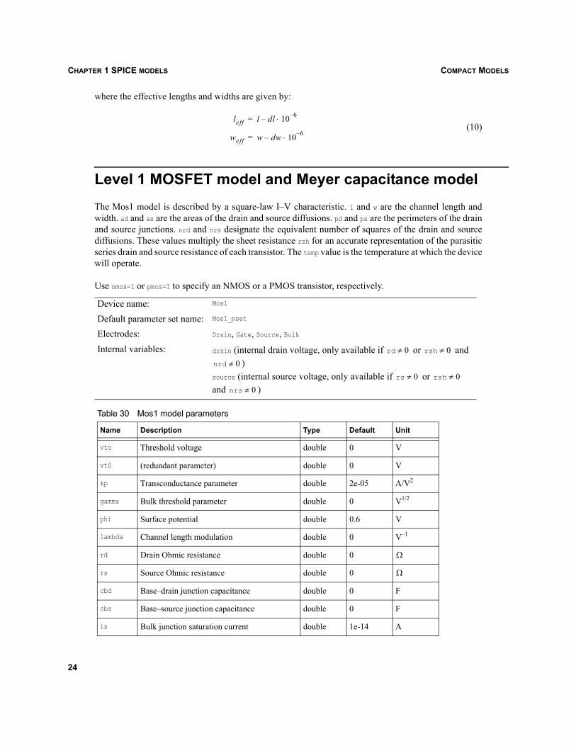
Level 1 MOSFET model and Meyer capacitance modelThe Mos1 model is described by a square-law I–V characteristic. l and w are the channel length andwidth. ad and as are the areas of the drain and source diffusions. pd and ps are the perimeters of the drainand source junctions. nrd and nrs designate the equivalent number of squares of the drain and sourcediffusions. These values multiply the sheet resistance rsh for an accurate representation of the parasiticseries drain and source resistance of each transistor. The temp value is the temperature at which the devicewill operate.
Use nmos=1 or pmos=1 to specify an NMOS or a PMOS transistor, respectively.
Device name: Mos1
Default parameter set name: Mos1_pset
Electrodes: Drain, Gate, Source, BulkInternal variables: drain (internal drain voltage, only available if or and
)source (internal source voltage, only available if or and )
Table 30 Mos1 model parameters
Name Description Type Default Unit
vto Threshold voltage double 0 V
vt0 (redundant parameter) double 0 V
kp Transconductance parameter double 2e-05 A/V2
gamma Bulk threshold parameter double 0 V1/2
phi Surface potential double 0.6 V
lambda Channel length modulation double 0 V–1
rd Drain Ohmic resistance double 0
rs Source Ohmic resistance double 0
cbd Base–drain junction capacitance double 0 F
cbs Base–source junction capacitance double 0 F
is Bulk junction saturation current double 1e-14 A
leff l dl 10 6–⋅–=
weff w dw 10 6–⋅–=
rd 0≠ rsh 0≠
nrd 0≠
rs 0≠ rsh 0≠
nrs 0≠
Ω
Ω
24

COMPACT MODELS CHAPTER 1 SPICE MODELS
pb Bulk junction potential double 0.8 V
cgso Gate–source overlap capacitance double 0 F/m
cgdo Gate–drain overlap capacitance double 0 F/m
cgbo Gate–bulk overlap capacitance double 0 F/m
rsh Sheet resistance double 0 /sq
cj Bottom junction capacitance per area double 0 F/m2
mj Bottom grading coefficient double 0.5 –
cjsw Side junction capacitance per area double 0 F/m
mjsw Side grading coefficient double 0.5 –
js Bulk junction saturation current density double 0 A/m2
tox Oxide thickness double 0 m
ld Lateral diffusion double 0 m
u0 Surface mobility double 0 cm2/V/s
uo (redundant parameter) double 0 cm2/V/s
fc Forward bias junction fit parameter double 0.5 –
nmos N-type MOSFET model integer 1 –
pmos P-type MOSFET model integer 0 –
nsub Substrate doping double 0 cm–3
tpg Gate type integer 0a –
nss Surface state density double 0 cm–2
tnom Parameter measurement temperature double 27 oC
kf Flicker noise coefficient double 0 –
af Flicker noise exponent double 1 –
a. 1: opposite to substrate; –1: same as substrate; 0: Al gate.
Table 31 Mos1 instance parameters
Name Description Type Default Unit
l Length double 0.0001 m
w Width double 0.0001 m
ad Drain area double 0 m2
Table 30 Mos1 model parameters
Name Description Type Default Unit
Ω
25

COMPACT MODELSCHAPTER 1 SPICE MODELS
Level 2 MOSFET model and Meyer capacitance modelThe Mos2 model is an analytic model [6]. l and w are the channel length and width. ad and as are theareas of the drain and source diffusions. pd and ps are the perimeters of the drain and source junctions.nrd and nrs designate the equivalent number of squares of the drain and source diffusions; these valuesmultiply the sheet resistance rsh for an accurate representation of the parasitic series drain and sourceresistance of each transistor. The temp value is the temperature at which the device will operate.
Use nmos=1 or pmos=1 to specify an NMOS or a PMOS transistor, respectively.
as Source area double 0 m2
pd Drain perimeter double 0 m
ps Source perimeter double 0 m
nrd Drain squares double 1 –
nrs Source squares double 1 –
off Device initially off integer – –
icvds Initial drain–source voltage double 0 V
icvgs Initial gate–source voltage double 0 V
icvbs Initial base–source voltage double 0 V
temp Instance temperature double 27 oC
ic Vector of D–S, G–S, B–S voltages double[3] – V
Device name: Mos2
Default parameter set name: Mos2_pset
Electrodes: Drain, Gate, Source, BulkInternal variables: internal#drain (internal drain voltage, only available if or
and )internal#source (internal source voltage, only available if or
and )
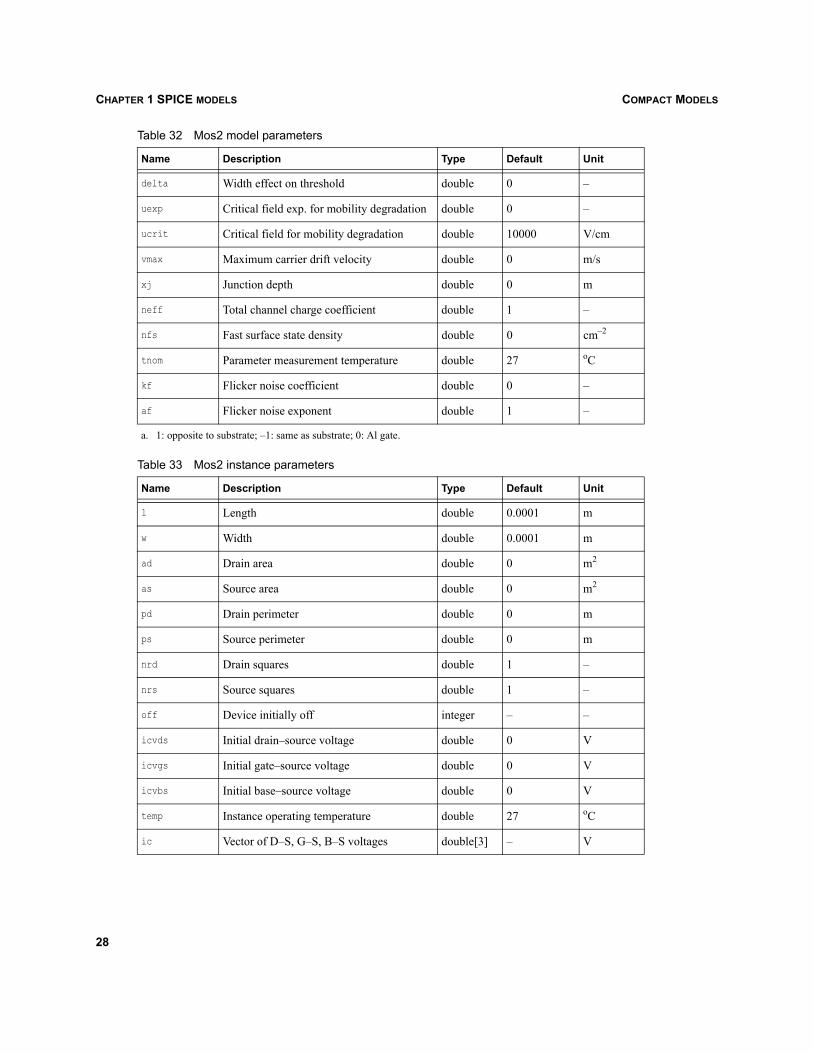
Table 32 Mos2 model parameters
Name Description Type Default Unit
vto Threshold voltage double 0 V
vt0 (redundant parameter) double 0 V
Table 31 Mos1 instance parameters
Name Description Type Default Unit
rd 0≠
rsh 0≠ nrd 0≠
rs 0≠
rsh 0≠ nrs 0≠
26

COMPACT MODELS CHAPTER 1 SPICE MODELS
kp Transconductance parameter double 2.07189e-05 A/V2
gamma Bulk threshold parameter double 0 V1/2
phi Surface potential double 0.6 V
lambda Channel length modulation double 0 V–1
rd Drain Ohmic resistance double 0
rs Source Ohmic resistance double 0
cbd Base–drain junction capacitance double 0 F
cbs Base–source junction capacitance double 0 F
is Bulk junction saturation current double 1e-14 A
pb Bulk junction potential double 0.8 V
cgso Gate–source overlap capacitance double 0 F/m
cgdo Gate–drain overlap capacitance double 0 F/m
cgbo Gate–bulk overlap capacitance double 0 F/m
rsh Sheet resistance double 0 /sq
cj Bottom junction capacitance per area double 0 F/m2
mj Bottom grading coefficient double 0.5 –
cjsw Side junction capacitance per area double 0 F/m
mjsw Side grading coefficient double 0.33 –
js Bulk junction saturation current density double 0 A/m2
tox Oxide thickness double 1e-07 m
ld Lateral diffusion double 0 m
u0 Surface mobility double 600 cm2/V/s
uo (redundant parameter) double 600 cm2/V/s
fc Forward bias junction fit parameter double 0.5 –
nmos N-type MOSFET model integer 1 –
pmos P-type MOSFET model integer 0 –
nsub Substrate doping double 0 cm–3
tpg Gate type integer 0a –
nss Surface state density double 0 cm–2
Table 32 Mos2 model parameters
Name Description Type Default Unit
Ω
Ω
Ω
27
COMPACT MODELSCHAPTER 1 SPICE MODELS
delta Width effect on threshold double 0 –
uexp Critical field exp. for mobility degradation double 0 –
ucrit Critical field for mobility degradation double 10000 V/cm
vmax Maximum carrier drift velocity double 0 m/s
xj Junction depth double 0 m
neff Total channel charge coefficient double 1 –
nfs Fast surface state density double 0 cm–2
tnom Parameter measurement temperature double 27 oC
kf Flicker noise coefficient double 0 –
af Flicker noise exponent double 1 –
a. 1: opposite to substrate; –1: same as substrate; 0: Al gate.
Table 33 Mos2 instance parameters
Name Description Type Default Unit
l Length double 0.0001 m
w Width double 0.0001 m
ad Drain area double 0 m2
as Source area double 0 m2
pd Drain perimeter double 0 m
ps Source perimeter double 0 m
nrd Drain squares double 1 –
nrs Source squares double 1 –
off Device initially off integer – –
icvds Initial drain–source voltage double 0 V
icvgs Initial gate–source voltage double 0 V
icvbs Initial base–source voltage double 0 V
temp Instance operating temperature double 27 oC
ic Vector of D–S, G–S, B–S voltages double[3] – V
Table 32 Mos2 model parameters
Name Description Type Default Unit
28

COMPACT MODELS CHAPTER 1 SPICE MODELS
Level 3 MOSFET model and Meyer capacitance modelThe Mos3 model is a semi-empirical model [6]. l and w are the channel length and width. ad and as arethe areas of the drain and source diffusions. pd and ps are the perimeters of the drain and source junctions.nrd and nrs designate the equivalent number of squares of the drain and source diffusions; these valuesmultiply the sheet resistance rsh for an accurate representation of the parasitic series drain and sourceresistance of each transistor. The temp value is the temperature at which the device will operate.
Use nmos=1 or pmos=1 to specify an NMOS or a PMOS transistor, respectively.
Device name: Mos3
Default parameter set name: Mos3_pset
Electrodes: Drain, Gate, Source, BulkInternal variables: internal#drain (internal drain voltage, only available if or
and )internal#source (internal source voltage, only available if or
and )
Table 34 Mos3 model parameters
Name Description Type Default Unit
nmos N-type MOSFET model integer 1 –
pmos P-type MOSFET model integer 0 –
vto Threshold voltage double 0 V
vt0 (redundant parameter) double 0 V
kp Transconductance parameter double 2.07189e-05 A/V2
gamma Bulk threshold parameter double 0 V1/2
phi Surface potential double 0.6 V
rd Drain Ohmic resistance double 0
rs Source Ohmic resistance double 0
cbd Base–drain junction capacitance double 0 F
cbs Base–source junction capacitance double 0 F
is Bulk junction saturation current double 1e-14 A
pb Bulk junction potential double 0.8 V
cgso Gate–source overlap capacitance double 0 F/m
cgdo Gate–drain overlap capacitance double 0 F/m
cgbo Gate–bulk overlap capacitance double 0 F/m
rd 0≠
rsh 0≠ nrd 0≠
rs 0≠
rsh 0≠ nrs 0≠
Ω
Ω
29

COMPACT MODELSCHAPTER 1 SPICE MODELS
rsh Sheet resistance double 0 /sq
cj Bottom junction capacitance per area double 0 F/m2
mj Bottom grading coefficient double 0.5 –
cjsw Side junction capacitance per area double 0 F/m
mjsw Side grading coefficient double 0.33 –
js Bulk junction saturation current density double 0 A/m2
tox Oxide thickness double 1e-07 m
ld Lateral diffusion double 0 m
u0 Surface mobility double 600 cm2/V/s
uo (redundant parameter) double 600 cm2/V/s
fc Forward bias junction fit parameter double 0.5 –
nsub Substrate doping double 0 cm–3
tpg Gate type integer 0a –
nss Surface state density double 0 cm–2
vmax Maximum carrier drift velocity double 0 m/s
xj Junction depth double 0 m
nfs Fast surface state density double 0 cm–2
xd Depletion layer width double 0 –
alpha Alpha double 0 –
eta Vds dependence of threshold voltage double 0 –
delta Width effect on threshold double 0 –
input_delta (redundant parameter) double 0 –
theta Vgs dependence on mobility double 0 V–1
kappa Kappa double 0.2 –
tnom Parameter measurement temperature double 27 oC
kf Flicker noise coefficient double 0 –
af Flicker noise exponent double 1 –
a. 1: opposite to substrate; –1: same as substrate; 0: Al gate.
Table 34 Mos3 model parameters
Name Description Type Default Unit
Ω
30
COMPACT MODELS CHAPTER 1 SPICE MODELS
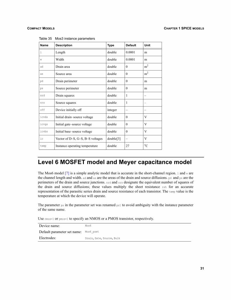
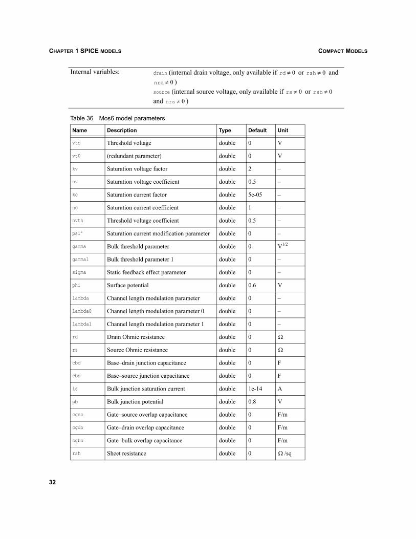
Level 6 MOSFET model and Meyer capacitance modelThe Mos6 model [7] is a simple analytic model that is accurate in the short-channel region. l and w arethe channel length and width. ad and as are the areas of the drain and source diffusions. pd and ps are theperimeters of the drain and source junctions. nrd and nrs designate the equivalent number of squares ofthe drain and source diffusions; these values multiply the sheet resistance rsh for an accuraterepresentation of the parasitic series drain and source resistance of each transistor. The temp value is thetemperature at which the device will operate.
The parameter ps in the parameter set was renamed ps1 to avoid ambiguity with the instance parameterof the same name.
Use nmos=1 or pmos=1 to specify an NMOS or a PMOS transistor, respectively.
Table 35 Mos3 instance parameters
Name Description Type Default Unit
l Length double 0.0001 m
w Width double 0.0001 m
ad Drain area double 0 m2
as Source area double 0 m2
pd Drain perimeter double 0 m
ps Source perimeter double 0 m
nrd Drain squares double 1 –
nrs Source squares double 1 –
off Device initially off integer – –
icvds Initial drain–source voltage double 0 V
icvgs Initial gate–source voltage double 0 V
icvbs Initial base–source voltage double 0 V
ic Vector of D–S, G–S, B–S voltages double[3] – V
temp Instance operating temperature double 27 oC
Device name: Mos6
Default parameter set name: Mos6_pset
Electrodes: Drain, Gate, Source, Bulk
31
COMPACT MODELSCHAPTER 1 SPICE MODELS
Internal variables: drain (internal drain voltage, only available if or and )
source (internal source voltage, only available if or and )
Table 36 Mos6 model parameters
Name Description Type Default Unit
vto Threshold voltage double 0 V
vt0 (redundant parameter) double 0 V
kv Saturation voltage factor double 2 –
nv Saturation voltage coefficient double 0.5 –
kc Saturation current factor double 5e-05 –
nc Saturation current coefficient double 1 –
nvth Threshold voltage coefficient double 0.5 –
ps1a Saturation current modification parameter double 0 –
gamma Bulk threshold parameter double 0 V1/2
gamma1 Bulk threshold parameter 1 double 0 –
sigma Static feedback effect parameter double 0 –
phi Surface potential double 0.6 V
lambda Channel length modulation parameter double 0 –
lambda0 Channel length modulation parameter 0 double 0 –
lambda1 Channel length modulation parameter 1 double 0 –
rd Drain Ohmic resistance double 0
rs Source Ohmic resistance double 0
cbd Base–drain junction capacitance double 0 F
cbs Base–source junction capacitance double 0 F
is Bulk junction saturation current double 1e-14 A
pb Bulk junction potential double 0.8 V
cgso Gate–source overlap capacitance double 0 F/m
cgdo Gate–drain overlap capacitance double 0 F/m
cgbo Gate–bulk overlap capacitance double 0 F/m
rsh Sheet resistance double 0 /sq
rd 0≠ rsh 0≠
nrd 0≠
rs 0≠ rsh 0≠
nrs 0≠
Ω
Ω
Ω
32
COMPACT MODELS CHAPTER 1 SPICE MODELS
cj Bottom junction capacitance per area double 0 F/m2
mj Bottom grading coefficient double 0.5 –
cjsw Side junction capacitance per area double 0 F/m
mjsw Side grading coefficient double 0.5 –
js Bulk junction saturation current density double 0 A/m2
ld Lateral diffusion double 0 m
tox Oxide thickness double 0 m
u0 Surface mobility double 0 cm2/V/s
uo (redundant parameter) double 0 cm2/V/s
fc Forward bias junction fit parameter double 0.5 –
nmos N-type MOSFET model integer 1 –
pmos P-type MOSFET model integer 0 –
tpg Gate type integer 0b –
nsub Substrate doping double 0 cm–3
nss Surface state density double 0 cm–2
tnom Parameter measurement temperature double 27 oC
a. Original SPICE name: ps.b. 1: opposite to substrate; –1: same as substrate; 0: Al gate.
Table 37 Mos6 instance parameters
Name Description Type Default Unit
l Length double 0.0001 m
w Width double 0.0001 m
ad Drain area double 0 m2
as Source area double 0 m2
pd Drain perimeter double 0 m
ps Source perimeter double 0 m
nrd Drain squares double 0 –
nrs Source squares double 0 –
off Device initially off integer – –
Table 36 Mos6 model parameters
Name Description Type Default Unit
33

COMPACT MODELSCHAPTER 1 SPICE MODELS
Berkeley short-channel IGFET model (BSIM1)The BSIM1 model [8][9][10] is a Berkeley short-channel IGFET model. In SPICE, this model issometimes called a level 4 MOSFET model. l and w are the channel length and width. ad and as are theareas of the drain and source diffusions. pd and ps are the perimeters of the drain and source junctions.nrd and nrs designate the equivalent number of squares of the drain and source diffusions; these valuesmultiply the sheet resistance rsh for an accurate representation of the parasitic series drain and sourceresistance of each transistor.
Use nmos=1 or pmos=1 to specify an NMOS or a PMOS transistor, respectively.
icvds Initial drain–source voltage double 0 V
icvgs Initial gate–source voltage double 0 V
icvbs Initial base–source voltage double 0 V
temp Instance temperature double 27 oC
ic Vector of D–S, G–S, B–S voltages double[3] – V
Device name: BSIM1
Default parameter set name: BSIM1_pset
Electrodes: Drain, Gate, Source, BulkInternal variables: drain (internal drain voltage, only available if and )
source (internal source voltage, only available if and )
Table 38 BSIM1 model parameters
Name Description Type Default Unit
vfb Flat-band voltage double 0 V
lvfb Length dependence of vfb double 0 V
wvfb Width dependence of vfb double 0 V
phi Strong inversion surface potential double 0 V
lphi Length dependence of phi double 0 V
wphi Width dependence of phi double 0 V
k1 Bulk effect coefficient 1 double 0 V1/2
lk1 Length dependence of k1 double 0 V1/2
Table 37 Mos6 instance parameters
Name Description Type Default Unit
rsh 0≠ nrd 0≠
rsh 0≠
nrs 0≠
μm
μm
μm
μm
μm
34
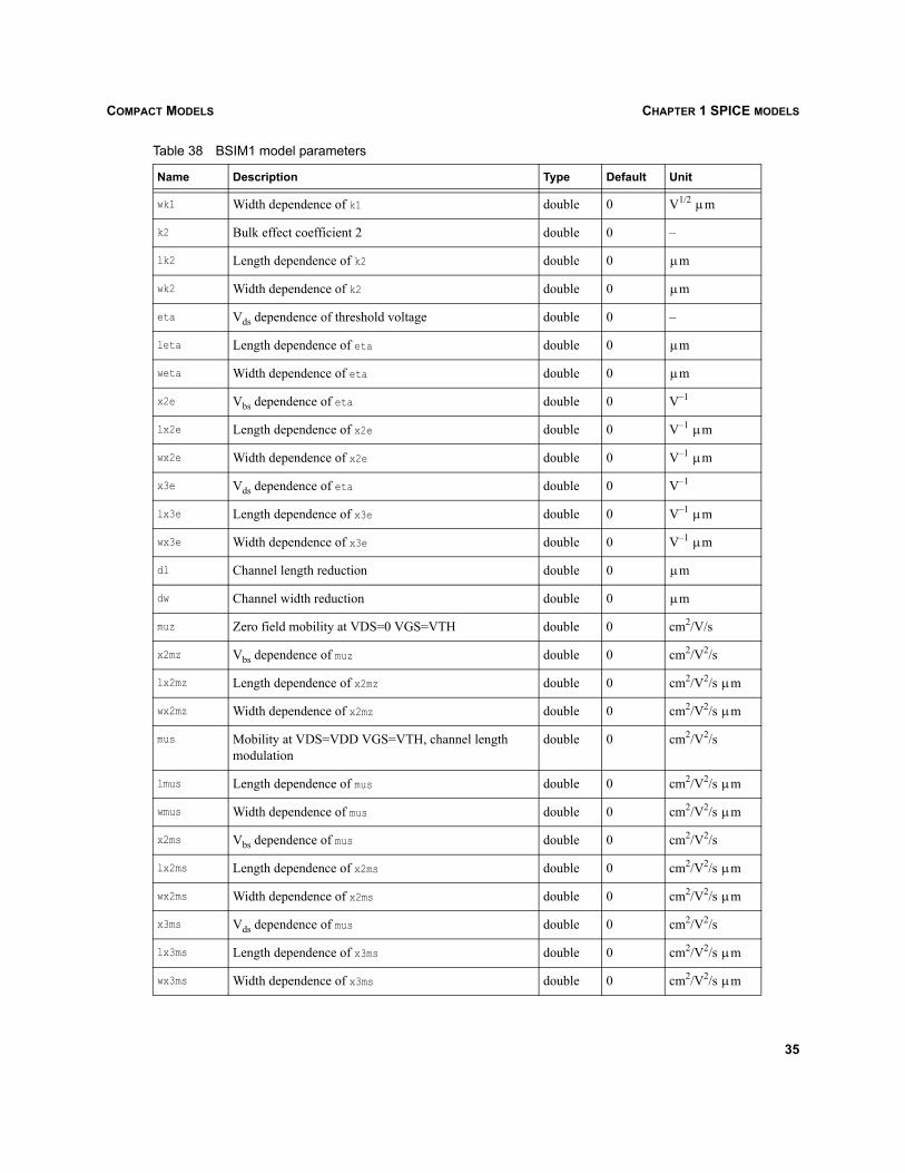
COMPACT MODELS CHAPTER 1 SPICE MODELS
wk1 Width dependence of k1 double 0 V1/2
k2 Bulk effect coefficient 2 double 0 –
lk2 Length dependence of k2 double 0
wk2 Width dependence of k2 double 0
eta Vds dependence of threshold voltage double 0 –
leta Length dependence of eta double 0
weta Width dependence of eta double 0
x2e Vbs dependence of eta double 0 V–1
lx2e Length dependence of x2e double 0 V–1
wx2e Width dependence of x2e double 0 V–1
x3e Vds dependence of eta double 0 V–1
lx3e Length dependence of x3e double 0 V–1
wx3e Width dependence of x3e double 0 V–1
dl Channel length reduction double 0
dw Channel width reduction double 0
muz Zero field mobility at VDS=0 VGS=VTH double 0 cm2/V/s
x2mz Vbs dependence of muz double 0 cm2/V2/s
lx2mz Length dependence of x2mz double 0 cm2/V2/s
wx2mz Width dependence of x2mz double 0 cm2/V2/s
mus Mobility at VDS=VDD VGS=VTH, channel length modulation
double 0 cm2/V2/s
lmus Length dependence of mus double 0 cm2/V2/s
wmus Width dependence of mus double 0 cm2/V2/s
x2ms Vbs dependence of mus double 0 cm2/V2/s
lx2ms Length dependence of x2ms double 0 cm2/V2/s
wx2ms Width dependence of x2ms double 0 cm2/V2/s
x3ms Vds dependence of mus double 0 cm2/V2/s
lx3ms Length dependence of x3ms double 0 cm2/V2/s
wx3ms Width dependence of x3ms double 0 cm2/V2/s
Table 38 BSIM1 model parameters
Name Description Type Default Unit
μm
μm
μm
μm
μm
μm
μm
μm
μm
μm
μm
μm
μm
μm
μm
μm
μm
μm
μm
35
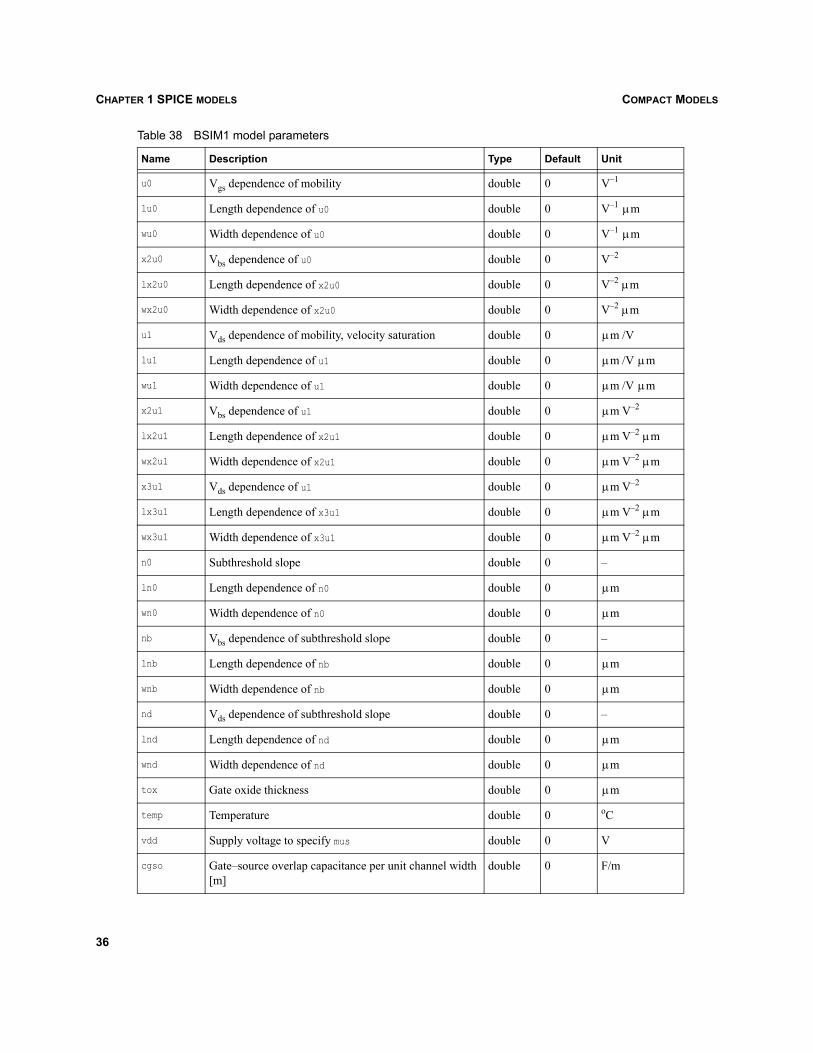
COMPACT MODELSCHAPTER 1 SPICE MODELS
u0 Vgs dependence of mobility double 0 V–1
lu0 Length dependence of u0 double 0 V–1
wu0 Width dependence of u0 double 0 V–1
x2u0 Vbs dependence of u0 double 0 V–2
lx2u0 Length dependence of x2u0 double 0 V–2
wx2u0 Width dependence of x2u0 double 0 V–2
u1 Vds dependence of mobility, velocity saturation double 0 /V
lu1 Length dependence of u1 double 0 /V
wu1 Width dependence of u1 double 0 /V
x2u1 Vbs dependence of u1 double 0 V–2
lx2u1 Length dependence of x2u1 double 0 V–2
wx2u1 Width dependence of x2u1 double 0 V–2
x3u1 Vds dependence of u1 double 0 V–2
lx3u1 Length dependence of x3u1 double 0 V–2
wx3u1 Width dependence of x3u1 double 0 V–2
n0 Subthreshold slope double 0 –
ln0 Length dependence of n0 double 0
wn0 Width dependence of n0 double 0
nb Vbs dependence of subthreshold slope double 0 –
lnb Length dependence of nb double 0
wnb Width dependence of nb double 0
nd Vds dependence of subthreshold slope double 0 –
lnd Length dependence of nd double 0
wnd Width dependence of nd double 0
tox Gate oxide thickness double 0
temp Temperature double 0 oC
vdd Supply voltage to specify mus double 0 V
cgso Gate–source overlap capacitance per unit channel width [m]
double 0 F/m
Table 38 BSIM1 model parameters
Name Description Type Default Unit
μm
μm
μm
μm
μm
μm μm
μm μm
μm
μm μm
μm μm
μm
μm μm
μm μm
μm
μm
μm
μm
μm
μm
μm
36

COMPACT MODELS CHAPTER 1 SPICE MODELS
cgdo Gate–drain overlap capacitance per unit channel width [m]
double 0 F/m
cgbo Gate–bulk overlap capacitance per unit channel length [m]
double 0 F/m
xpart Flag for channel charge partitioning integer 0a –
rsh Source–drain diffusion sheet resistance double 0 /sq
js Source–drain junction saturation current per unit area double 0 A/m2
pb Source–drain junction built-in potential double 0.1 V
mj Source–drain bottom junction capacitance grading coefficient
double 0 –
pbsw Source–drain side junction capacitance built-in potential double 0.1 V
mjsw Source–drain side junction capacitance grading coefficient
double 0 –
cj Source–drain bottom junction capacitance per unit area double 0 F/m2
cjsw Source–drain side junction capacitance per unit area double 0 F/m2
wdf Default width of source–drain diffusion in μm double 0 m
dell Length reduction of source–drain diffusion double 0 m
nmos Flag to indicate NMOS integer 1 –
pmos Flag to indicate PMOS integer 0 –
a. The parameter xpart describes the channel charge partitioning. xpart=0 selects a 40/60 drain/sourcecharge partition in saturation, while xpart=1 selects a 0/100 drain/source charge partition.
Table 39 BSIM1 instance parameters
Name Description Type Default Unit
l Length double 5e-06 m
w Width double 5e-06 m
ad Drain area double 0 m2
as Source area double 0 m2
pd Drain perimeter double 0 m
ps Source perimeter double 0 m
nrd Number of squares in drain double 1 –
nrs Number of squares in source double 1 –
Table 38 BSIM1 model parameters
Name Description Type Default Unit
Ω
37

COMPACT MODELSCHAPTER 1 SPICE MODELS
Berkeley short-channel IGFET model (BSIM2)The BSIM2 model [11] is a Berkeley short-channel IGFET model. In SPICE, this model is sometimescalled a level 5 MOSFET model. l and w are the channel length and width. ad and as are the areas of thedrain and source diffusions. pd and ps are the perimeters of the drain and source junctions. nrd and nrsdesignate the equivalent number of squares of the drain and source diffusions; these values multiply thesheet resistance rsh for an accurate representation of the parasitic series drain and source resistance ofeach transistor.
Use nmos=1 or pmos=1 to specify an NMOS or a PMOS transistor, respectively.
off Device is initially off integer 0 –
vds Initial drain–source voltage double 0 V
vgs Initial gate–source voltage double 0 V
vbs Initial base–source voltage double 0 V
ic Vector of D–S, G–S, B–S initial voltages double[3] – V
Device name: BSIM2
Default parameter set name: BSIM2_pset
Electrodes: Drain, Gate, Source, BulkInternal variables: drain (internal drain voltage, only available if and )
source (internal source voltage, only available if and )
Table 40 BSIM2 model parameters
Name Description Type Default Unit
vfb Flat-band voltage double –1 V
lvfb Length dependence of vfb double 0 V
wvfb Width dependence of vfb double 0 V
phi Strong inversion surface potential double 0.75 V
lphi Length dependence of phi double 0 V
wphi Width dependence of phi double 0 V
k1 Bulk effect coefficient 1 double 0.8 V1/2
lk1 Length dependence of k1 double 0 V1/2
Table 39 BSIM1 instance parameters
Name Description Type Default Unit
rsh 0≠ nrd 0≠
rsh 0≠
nrs 0≠
μm
μm
μm
μm
μm
38

COMPACT MODELS CHAPTER 1 SPICE MODELS
wk1 Width dependence of k1 double 0 V1/2
k2 Bulk effect coefficient 2 double 0 –
lk2 Length dependence of k2 double 0
wk2 Width dependence of k2 double 0
eta0 Vds dependence of threshold voltage at VDD=0 double 0 –
leta0 Length dependence of eta0 double 0
weta0 Width dependence of eta0 double 0
etab Vbs dependence of eta double 0 –
letab Length dependence of etab double 0 –
wetab Width dependence of etab double 0 –
dl Channel length reduction double 0
dw Channel width reduction double 0
mu0 Low-field mobility, at VDS=0 VGS=VTH double 400 cm2/V2/s
mu0b Vbs dependence of low-field mobility double 0 –
lmu0b Length dependence of mu0b double 0 –
wmu0b Width dependence of mu0b double 0 –
mus0 Mobility at VDS=VDD VGS=VTH double 500 cm2/V2/s
lmus0 Length dependence of mus0 double 0 –
wmus0 Width dependence of mus double 0 –
musb Vbs dependence of mus double 0 –
lmusb Length dependence of musb double 0 –
wmusb Width dependence of musb double 0 –
mu20 Vds dependence of mu in tanh term double 1.5 –
lmu20 Length dependence of mu20 double 0 –
wmu20 Width dependence of mu20 double 0 –
mu2b Vbs dependence of mu2 double 0 –
lmu2b Length dependence of mu2b double 0 –
wmu2b Width dependence of mu2b double 0 –
mu2g Vgs dependence of mu2 double 0 –
Table 40 BSIM2 model parameters
Name Description Type Default Unit
μm
μm
μm
μm
μm
μm
μm
39

COMPACT MODELSCHAPTER 1 SPICE MODELS
lmu2g Length dependence of mu2g double 0 –
wmu2g Width dependence of mu2g double 0 –
mu30 Vds dependence of mu in linear term double 10 –
lmu30 Length dependence of mu30 double 0 –
wmu30 Width dependence of mu30 double 0 –
mu3b Vbs dependence of mu3 double 0 –
lmu3b Length dependence of mu3b double 0 –
wmu3b Width dependence of mu3b double 0 –
mu3g Vgs dependence of mu3 double 0 –
lmu3g Length dependence of mu3g double 0 –
wmu3g Width dependence of mu3g double 0 –
mu40 Vds dependence of mu in linear term double 0 –
lmu40 Length dependence of mu40 double 0 –
wmu40 Width dependence of mu40 double 0 –
mu4b Vbs dependence of mu4 double 0 –
lmu4b Length dependence of mu4b double 0 –
wmu4b Width dependence of mu4b double 0 –
mu4g Vgs dependence of mu4 double 0 –
lmu4g Length dependence of mu4g double 0 –
wmu4g Width dependence of mu4g double 0 –
ua0 Linear Vgs dependence of mobility double 0.2 –
lua0 Length dependence of ua0 double 0 –
wua0 Width dependence of ua0 double 0 –
uab Vbs dependence of ua double 0 –
luab Length dependence of uab double 0 –
wuab Width dependence of uab double 0 –
ub0 Quadratic Vgs dependence of mobility double 0 –
lub0 Length dependence of ub0 double 0 –
wub0 Width dependence of ub0 double 0 –
Table 40 BSIM2 model parameters
Name Description Type Default Unit
40

COMPACT MODELS CHAPTER 1 SPICE MODELS
ubb Vbs dependence of ub double 0 –
lubb Length dependence of ubb double 0 –
wubb Width dependence of ubb double 0 –
u10 Vds dependence of mobility double 0.1 –
lu10 Length dependence of u10 double 0 –
wu10 Width dependence of u10 double 0 –
u1b Vbs dependence of u1 double 0 –
lu1b Length dependence of u1b double 0 –
wu1b Width dependence of u1b double 0 –
u1d Vds dependence of u1 double 0 –
lu1d Length dependence of u1d double 0 –
wu1d Width dependence of u1d double 0 –
n0 Subthreshold slope at VDS=0 VBS=0 double 1.4 –
ln0 Length dependence of n0 double 0 –
wn0 Width dependence of n0 double 0 –
nb Vbs dependence of n double 0.5 –
lnb Length dependence of nb double 0 –
wnb Width dependence of nb double 0 –
nd Vds dependence of n double 0 –
lnd Length dependence of nd double 0 –
wnd Width dependence of nd double 0 –
vof0 Threshold voltage offset at VDS=0 VBS=0 double 1.8 –
lvof0 Length dependence of vof0 double 0 –
wvof0 Width dependence of vof0 double 0 –
vofb Vbs dependence of vof double 0 –
lvofb Length dependence of vofb double 0 –
wvofb Width dependence of vofb double 0 –
vofd Vds dependence of vof double 0 –
lvofd Length dependence of vofd double 0 –
Table 40 BSIM2 model parameters
Name Description Type Default Unit
41

COMPACT MODELSCHAPTER 1 SPICE MODELS
wvofd Width dependence of vofd double 0 –
ai0 Prefactor of hot-electron effect double 0 –
lai0 Length dependence of ai0 double 0 –
wai0 Width dependence of ai0 double 0 –
aib Vbs dependence of ai double 0 –
laib Length dependence of aib double 0 –
waib Width dependence of aib double 0 –
bi0 Exponential factor of hot-electron effect double 0 –
lbi0 Length dependence of bi0 double 0 –
wbi0 Width dependence of bi0 double 0 –
bib Vbs dependence of bi double 0 –
lbib Length dependence of bib double 0 –
wbib Width dependence of bib double 0 –
vghigh Upper bound of cubic spline function double 0.2 –
lvghigh Length dependence of vghigh double 0 –
wvghigh Width dependence of vghigh double 0 –
vglow Lower bound of cubic spline function double –0.15 –
lvglow Length dependence of vglow double 0 –
wvglow Width dependence of vglow double 0 –
tox Gate oxide thickness double 0.03
temp Temperature double 27 oC
vdd Maximum Vds double 5 V
vgg Maximum Vgs double 5 V
vbb Maximum Vbs double 5 V
cgso Gate–source overlap capacitance per unit channel width [m]
double 0 F/m
cgdo Gate–drain overlap capacitance per unit channel width [m]
double 0 F/m
cgbo Gate–bulk overlap capacitance per unit channel length [m]
double 0 F/m
Table 40 BSIM2 model parameters
Name Description Type Default Unit
μm
42

COMPACT MODELS CHAPTER 1 SPICE MODELS
xpart Flag for channel charge partitioning integer 0a –
rsh Source–drain diffusion sheet resistance double 0 /sq
js Source–drain junction saturation current per unit area
double 0 A/m2
pb Source–drain junction built-in potential double 0.1 V
mj Source–drain bottom junction capacitance grading coefficient
double 0 –
pbsw Source–drain side junction capacitance built-in potential
double 0.1 V
mjsw Source–drain side junction capacitance grading coefficient
double 0 –
cj Source–drain bottom junction capacitance per unit area
double 0 F/m2
cjsw Source–drain side junction capacitance per unit area double 0 F/m
wdf Default width of source–drain diffusion double 10
dell Length reduction of source–drain diffusion double 0 m
nmos Flag to indicate NMOS integer 1 –
pmos Flag to indicate PMOS integer 0 –
a. The parameter xpart describes the channel charge partitioning. xpart=0 selects a 40/60 drain/sourcecharge partition in saturation, while xpart=1 selects a 0/100 drain/source charge partition.
Table 41 BSIM2 instance parameters
Name Description Type Default Unit
l Length double 5e-06 m
w Width double 5e-06 m
ad Drain area double 0 m2
as Source area double 0 m2
pd Drain perimeter double 0 m
ps Source perimeter double 0 m
nrd Number of squares in drain double 1 –
nrs Number of squares in source double 1 –
off Device is initially off integer 0 –
Table 40 BSIM2 model parameters
Name Description Type Default Unit
Ω
μm
43

COMPACT MODELSCHAPTER 1 SPICE MODELS
Berkeley short-channel IGFET model version 3 (BSIM3)The BSIM3 model is the latest physics-based MOSFET SPICE model for circuit simulation and CMOStechnology development. In SPICE, this model is also called a level 8 MOSFET model.
Use nmos=1 or pmos=1 to specify an NMOS or a PMOS transistor, respectively.
vds Initial drain–source voltage double 0 V
vgs Initial gate–source voltage double 0 V
vbs Initial base–source voltage double 0 V
ic Vector of D–S, G–S, B–S initial voltages double[3] – V
Device name: BSIM3
Default parameter set name: BSIM3_pset
Electrodes: Drain, Gate, Source, BulkInternal variables: drain (internal drain voltage, only available if and )
source (internal source voltage, only available if and )
charge (internal charge node, only available if )
Table 42 BSIM3 model parameters
Name Description Type Default Unit
capmod Capacitance model selector integer 3 –
mobmod Mobility model selector integer 1 –
noimod Noise model selector integer 1 –
paramchk Model parameter checking selector integer 0 –
binunit Bin unit selector integer 1 –
version Parameter for model version double 3.2 –
tox Gate oxide thickness double 1.5e-08 m
toxm Gate oxide thickness used in extraction double 1.5e-08 m
cdsc Drain–source and channel coupling capacitance double 0.00024 F/m2
cdscb Body-bias dependence of cdsc double 0 F/V/m2
cdscd Drain-bias dependence of cdsc double 0 F/V/m2
Table 41 BSIM2 instance parameters
Name Description Type Default Unit
rsh 0> nrd 0>
rsh 0>
nrs 0>
nqsmod 0≠
44
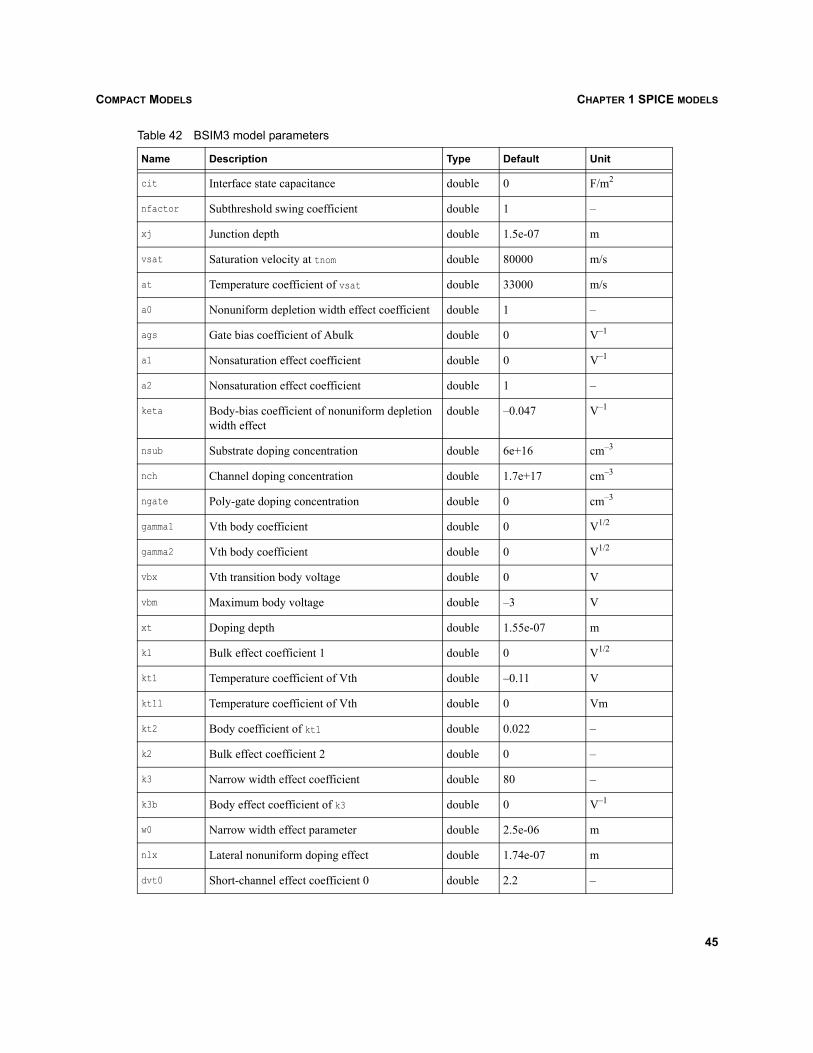
COMPACT MODELS CHAPTER 1 SPICE MODELS
cit Interface state capacitance double 0 F/m2
nfactor Subthreshold swing coefficient double 1 –
xj Junction depth double 1.5e-07 m
vsat Saturation velocity at tnom double 80000 m/s
at Temperature coefficient of vsat double 33000 m/s
a0 Nonuniform depletion width effect coefficient double 1 –
ags Gate bias coefficient of Abulk double 0 V–1
a1 Nonsaturation effect coefficient double 0 V–1
a2 Nonsaturation effect coefficient double 1 –
keta Body-bias coefficient of nonuniform depletion width effect
double –0.047 V–1
nsub Substrate doping concentration double 6e+16 cm–3
nch Channel doping concentration double 1.7e+17 cm–3
ngate Poly-gate doping concentration double 0 cm–3
gamma1 Vth body coefficient double 0 V1/2
gamma2 Vth body coefficient double 0 V1/2
vbx Vth transition body voltage double 0 V
vbm Maximum body voltage double –3 V
xt Doping depth double 1.55e-07 m
k1 Bulk effect coefficient 1 double 0 V1/2
kt1 Temperature coefficient of Vth double –0.11 V
kt1l Temperature coefficient of Vth double 0 Vm
kt2 Body coefficient of kt1 double 0.022 –
k2 Bulk effect coefficient 2 double 0 –
k3 Narrow width effect coefficient double 80 –
k3b Body effect coefficient of k3 double 0 V–1
w0 Narrow width effect parameter double 2.5e-06 m
nlx Lateral nonuniform doping effect double 1.74e-07 m
dvt0 Short-channel effect coefficient 0 double 2.2 –
Table 42 BSIM3 model parameters
Name Description Type Default Unit
45

COMPACT MODELSCHAPTER 1 SPICE MODELS
dvt1 Short-channel effect coefficient 1 double 0.53 –
dvt2 Short-channel effect coefficient 2 double –0.032 V–1
dvt0w Narrow width coefficient 0 double 0 m–1
dvt1w Narrow width effect coefficient 1 double 5.3e+06 m–1
dvt2w Narrow width effect coefficient 2 double –0.032 V–1
drout DIBL coefficient of output resistance double 0.56 –
dsub DIBL coefficient in subthreshold region double drout –
vth0 Threshold voltage double 0.7a V
vtho (redundant parameter) double 0.7 V
ua Linear gate dependence of mobility double 2.25e-09 m/V
ua1 Temperature coefficient of ua double 4.31e-09 m/V
ub Quadratic gate dependence of mobility double 5.87e-19 (m/V)2
ub1 Temperature coefficient of ub double –7.61e-18 (m/V)2
uc Body-bias dependence of mobility double –4.65e-11b m/V2
uc1 Temperature coefficient of uc double –5.6e-11c m/V2
u0 Low-field mobility at tnom double 0.067d cm2/V/s
ute Temperature coefficient of mobility double –1.5 –
voff Threshold voltage offset double –0.08 V
tnom Parameter measurement temperature double 27 oC
cgso Gate–source overlap capacitance per width double 2.07188e-10 F/m
cgdo Gate–drain overlap capacitance per width double 2.07188e-10 F/m
cgbo Gate–bulk overlap capacitance per length double 0 F/m
xpart Channel charge partitioning double 0e –
elm Non-quasistatic Elmore constant parameter double 5 –
delta Effective Vds parameter double 0.01 V
rsh Source–drain sheet resistance double 0 /sq
rdsw Source–drain resistance per width double 0 /
prwg Gate-bias effect on parasitic resistance double 0 V–1
prwb Body effect on parasitic resistance double 0 V–1/2
Table 42 BSIM3 model parameters
Name Description Type Default Unit
Ω
Ω μmwr
46

COMPACT MODELS CHAPTER 1 SPICE MODELS
prt Temperature coefficient of parasitic resistance double 0 /
eta0 Subthreshold region DIBL coefficient double 0.08 –
etab Subthreshold region DIBL coefficient double –0.07 V–1
pclm Channel-length modulation coefficient double 1.3 –
pdiblc1 Drain-induced barrier-lowering coefficient double 0.39 –
pdiblc2 Drain-induced barrier-lowering coefficient double 0.0086 –
pdiblcb Body effect on drain-induced barrier lowering double 0 V–1
pscbe1 Substrate current body-effect coefficient double 4.24e+08 V/m
pscbe2 Substrate current body-effect coefficient double 1e-05 m/V
pvag Gate dependence of output resistance parameter double 0 –
js Source–drain junction reverse saturation current density
double 0.0001 A/m2
jsw Sidewall junction reverse saturation current density
double 0 A/m
pb Source–drain junction built-in potential double 1 V
nj Source–drain junction emission coefficient double 1 –
xti Junction current temperature exponent double 3 –
mj Source–drain bottom junction capacitance grading coefficient
double 0.5 –
pbsw Source–drain sidewall junction capacitance built-in potential
double 1 V
mjsw Source–drain sidewall junction capacitance grading coefficient
double 0.33 –
pbswg Source–drain (gate side) sidewall junction capacitance built-in potential
double pbsw V
mjswg Source–drain (gate side) sidewall junction capacitance grading coefficient
double mjsw –
cj Source–drain bottom junction capacitance per unit area
double 0.0005 F/m2
vfbcv Flat-band voltage parameter for capmod=0 only double –1 –
vfb Flat-band voltage double 0 V
Table 42 BSIM3 model parameters
Name Description Type Default Unit
Ω μm
47

COMPACT MODELSCHAPTER 1 SPICE MODELS
cjsw Source–drain sidewall junction capacitance per unit periphery
double 5e-10 F/m
cjswg Source–drain (gate side) sidewall junction capacitance per unit width
double cjsw F/m
tpb Temperature coefficient of pb double 0 –
tcj Temperature coefficient of cj double 0 –
tpbsw Temperature coefficient of pbsw double 0 –
tcjsw Temperature coefficient of cjsw double 0 –
tpbswg Temperature coefficient of pbswg double 0 –
tcjswg Temperature coefficient of cjswg double 0 –
acde Exponential coefficient for finite charge thickness
double 1 –
moin Coefficient for gate bias–dependent surface potential
double 15 –
noff C–V switch on and off parameter double 1 –
voffcv C–V lateral-shift parameter double 0 –
lint Length reduction parameter double 0 m
ll Length reduction parameter double 0
llc Length reduction parameter for C–V double 0 –
lln Length reduction parameter double 1 –
lw Length reduction parameter double 0
lwc Length reduction parameter for C–V double 0 –
lwn Length reduction parameter double 1 –
lwl Length reduction parameter double 0
lwlc Length reduction parameter for C–V double 0 –
lmin Minimum length of model double 0 m
lmax Maximum length of model double 1 m
wr Width dependence of rds double 1 –
wint Width reduction parameter double 0 m
dwg Width reduction parameter double 0 m/V
Table 42 BSIM3 model parameters
Name Description Type Default Unit
mlln
mlwn
mlwn+lln
48

COMPACT MODELS CHAPTER 1 SPICE MODELS
dwb Width reduction parameter double 0 m/V1/2
wl Width reduction parameter double 0
wlc Width reduction parameter for C–V double 0 –
wln Width reduction parameter double 1 –
ww Width reduction parameter double 0
wwc Width reduction parameter for C–V double 0 –
wwn Width reduction parameter double 1 –
wwl Width reduction parameter double 0
wwlc Width reduction parameter for C–V double 0 –
wmin Minimum width of model double 0 m
wmax Maximum width of model double 1 m
b0 Abulk narrow width parameter double 0 m
b1 Abulk narrow width parameter double 0 m
cgsl New C–V model parameter double 0 F/m
cgdl New C–V model parameter double 0 F/m
ckappa New C–V model parameter double 0.6 –
cf Fringe capacitance parameter double 7.29897e-11 F/m
clc Vdsat parameter for C–V model double 1e-07 m
cle Vdsat parameter for C–V model double 0.6 –
dwc Delta W for C–V model double wint m
dlc Delta L for C–V model double lint m
alpha0 Substrate current model parameter double 0 m/V
alpha1 Substrate current model parameter double 0 –
beta0 Substrate current model parameter double 30 V
ijth Diode-limiting current double 0.1 –
lcdsc Length dependence of cdsc double 0 –
lcdscb Length dependence of cdscb double 0 –
lcdscd Length dependence of cdscd double 0 –
lcit Length dependence of cit double 0 –
Table 42 BSIM3 model parameters
Name Description Type Default Unit
mwln
mwwn
mwwn+wln
49

COMPACT MODELSCHAPTER 1 SPICE MODELS
lnfactor Length dependence of nfactor double 0 –
lxj Length dependence of xj double 0 –
lvsat Length dependence of vsat double 0 –
lat Length dependence of at double 0 –
la0 Length dependence of a0 double 0 –
lags Length dependence of ags double 0 –
la1 Length dependence of a1 double 0 –
la2 Length dependence of a2 double 0 –
lketa Length dependence of keta double 0 –
lnsub Length dependence of nsub double 0 –
lnch Length dependence of nch double 0 –
lngate Length dependence of ngate double 0 –
lgamma1 Length dependence of gamma1 double 0 –
lgamma2 Length dependence of gamma2 double 0 –
lvbx Length dependence of vbx double 0 –
lvbm Length dependence of vbm double 0 –
lxt Length dependence of xt double 0 –
lk1 Length dependence of k1 double 0 –
lkt1 Length dependence of kt1 double 0 –
lkt1l Length dependence of kt1l double 0 –
lkt2 Length dependence of kt2 double 0 –
lk2 Length dependence of k2 double 0 –
lk3 Length dependence of k3 double 0 –
lk3b Length dependence of k3b double 0 –
lw0 Length dependence of w0 double 0 –
lnlx Length dependence of nlx double 0 –
ldvt0 Length dependence of dvt0 double 0 –
ldvt1 Length dependence of dvt1 double 0 –
ldvt2 Length dependence of dvt2 double 0 –
Table 42 BSIM3 model parameters
Name Description Type Default Unit
50
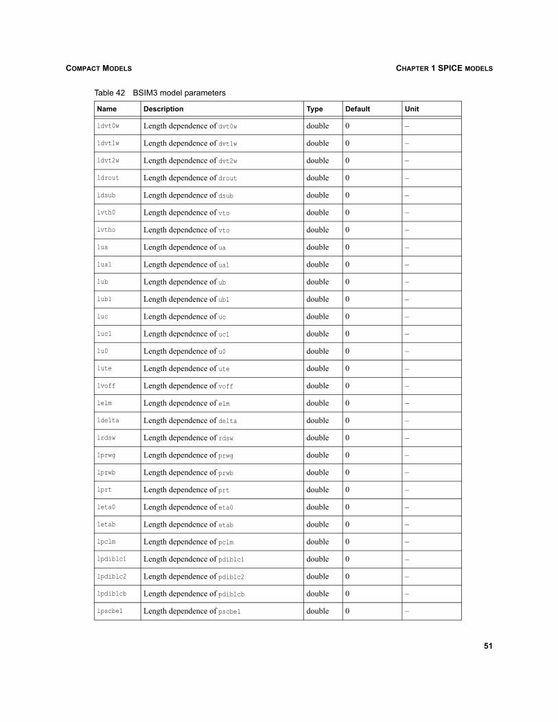
COMPACT MODELS CHAPTER 1 SPICE MODELS
ldvt0w Length dependence of dvt0w double 0 –
ldvt1w Length dependence of dvt1w double 0 –
ldvt2w Length dependence of dvt2w double 0 –
ldrout Length dependence of drout double 0 –
ldsub Length dependence of dsub double 0 –
lvth0 Length dependence of vto double 0 –
lvtho Length dependence of vto double 0 –
lua Length dependence of ua double 0 –
lua1 Length dependence of ua1 double 0 –
lub Length dependence of ub double 0 –
lub1 Length dependence of ub1 double 0 –
luc Length dependence of uc double 0 –
luc1 Length dependence of uc1 double 0 –
lu0 Length dependence of u0 double 0 –
lute Length dependence of ute double 0 –
lvoff Length dependence of voff double 0 –
lelm Length dependence of elm double 0 –
ldelta Length dependence of delta double 0 –
lrdsw Length dependence of rdsw double 0 –
lprwg Length dependence of prwg double 0 –
lprwb Length dependence of prwb double 0 –
lprt Length dependence of prt double 0 –
leta0 Length dependence of eta0 double 0 –
letab Length dependence of etab double 0 –
lpclm Length dependence of pclm double 0 –
lpdiblc1 Length dependence of pdiblc1 double 0 –
lpdiblc2 Length dependence of pdiblc2 double 0 –
lpdiblcb Length dependence of pdiblcb double 0 –
lpscbe1 Length dependence of pscbe1 double 0 –
Table 42 BSIM3 model parameters
Name Description Type Default Unit
51

COMPACT MODELSCHAPTER 1 SPICE MODELS
lpscbe2 Length dependence of pscbe2 double 0 –
lpvag Length dependence of pvag double 0 –
lwr Length dependence of wr double 0 –
ldwg Length dependence of dwg double 0 –
ldwb Length dependence of dwb double 0 –
lb0 Length dependence of b0 double 0 –
lb1 Length dependence of b1 double 0 –
lcgsl Length dependence of cgsl double 0 –
lcgdl Length dependence of cgdl double 0 –
lckappa Length dependence of ckappa double 0 –
lcf Length dependence of cf double 0 –
lclc Length dependence of clc double 0 –
lcle Length dependence of cle double 0 –
lalpha0 Length dependence of alpha0 double 0 –
lalpha1 Length dependence of alpha1 double 0 –
lbeta0 Length dependence of beta0 double 0 –
lvfbcv Length dependence of vfbcv double 0 –
lvfb Length dependence of vfb double 0 –
lacde Length dependence of acde double 0 –
lmoin Length dependence of moin double 0 –
lnoff Length dependence of noff double 0 –
lvoffcv Length dependence of voffcv double 0 –
wcdsc Width dependence of cdsc double 0 –
wcdscb Width dependence of cdscb double 0 –
wcdscd Width dependence of cdscd double 0 –
wcit Width dependence of cit double 0 –
wnfactor Width dependence of nfactor double 0 –
wxj Width dependence of xj double 0 –
wvsat Width dependence of vsat double 0 –
Table 42 BSIM3 model parameters
Name Description Type Default Unit
52

COMPACT MODELS CHAPTER 1 SPICE MODELS
wat Width dependence of at double 0 –
wa0 Width dependence of a0 double 0 –
wags Width dependence of ags double 0 –
wa1 Width dependence of a1 double 0 –
wa2 Width dependence of a2 double 0 –
wketa Width dependence of keta double 0 –
wnsub Width dependence of nsub double 0 –
wnch Width dependence of nch double 0 –
wngate Width dependence of ngate double 0 –
wgamma1 Width dependence of gamma1 double 0 –
wgamma2 Width dependence of gamma2 double 0 –
wvbx Width dependence of vbx double 0 –
wvbm Width dependence of vbm double 0 –
wxt Width dependence of xt double 0 –
wk1 Width dependence of k1 double 0 –
wkt1 Width dependence of kt1 double 0 –
wkt1l Width dependence of kt1l double 0 –
wkt2 Width dependence of kt2 double 0 –
wk2 Width dependence of k2 double 0 –
wk3 Width dependence of k3 double 0 –
wk3b Width dependence of k3b double 0 –
ww0 Width dependence of w0 double 0 –
wnlx Width dependence of nlx double 0 –
wdvt0 Width dependence of dvt0 double 0 –
wdvt1 Width dependence of dvt1 double 0 –
wdvt2 Width dependence of dvt2 double 0 –
wdvt0w Width dependence of dvt0w double 0 –
wdvt1w Width dependence of dvt1w double 0 –
wdvt2w Width dependence of dvt2w double 0 –
Table 42 BSIM3 model parameters
Name Description Type Default Unit
53

COMPACT MODELSCHAPTER 1 SPICE MODELS
wdrout Width dependence of drout double 0 –
wdsub Width dependence of dsub double 0 –
wvth0 Width dependence of vto double 0 –
wvtho Width dependence of vto double 0 –
wua Width dependence of ua double 0 –
wua1 Width dependence of ua1 double 0 –
wub Width dependence of ub double 0 –
wub1 Width dependence of ub1 double 0 –
wuc Width dependence of uc double 0 –
wuc1 Width dependence of uc1 double 0 –
wu0 Width dependence of u0 double 0 –
wute Width dependence of ute double 0 –
wvoff Width dependence of voff double 0 –
welm Width dependence of elm double 0 –
wdelta Width dependence of delta double 0 –
wrdsw Width dependence of rdsw double 0 –
wprwg Width dependence of prwg double 0 –
wprwb Width dependence of prwb double 0 –
wprt Width dependence of prt double 0 –
weta0 Width dependence of eta0 double 0 –
wetab Width dependence of etab double 0 –
wpclm Width dependence of pclm double 0 –
wpdiblc1 Width dependence of pdiblc1 double 0 –
wpdiblc2 Width dependence of pdiblc2 double 0 –
wpdiblcb Width dependence of pdiblcb double 0 –
wpscbe1 Width dependence of pscbe1 double 0 –
wpscbe2 Width dependence of pscbe2 double 0 –
wpvag Width dependence of pvag double 0 –
wwr Width dependence of wr double 0 –
Table 42 BSIM3 model parameters
Name Description Type Default Unit
54

COMPACT MODELS CHAPTER 1 SPICE MODELS
wdwg Width dependence of dwg double 0 –
wdwb Width dependence of dwb double 0 –
wb0 Width dependence of b0 double 0 –
wb1 Width dependence of b1 double 0 –
wcgsl Width dependence of cgsl double 0 –
wcgdl Width dependence of cgdl double 0 –
wckappa Width dependence of ckappa double 0 –
wcf Width dependence of cf double 0 –
wclc Width dependence of clc double 0 –
wcle Width dependence of cle double 0 –
walpha0 Width dependence of alpha0 double 0 –
walpha1 Width dependence of alpha1 double 0 –
wbeta0 Width dependence of beta0 double 0 –
wvfbcv Width dependence of vfbcv double 0 –
wvfb Width dependence of vfb double 0 –
wacde Width dependence of acde double 0 –
wmoin Width dependence of moin double 0 –
wnoff Width dependence of noff double 0 –
wvoffcv Width dependence of voffcv double 0 –
pcdsc Cross-term dependence of cdsc double 0 –
pcdscb Cross-term dependence of cdscb double 0 –
pcdscd Cross-term dependence of cdscd double 0 –
pcit Cross-term dependence of cit double 0 –
pnfactor Cross-term dependence of nfactor double 0 –
pxj Cross-term dependence of xj double 0 –
pvsat Cross-term dependence of vsat double 0 –
pat Cross-term dependence of at double 0 –
pa0 Cross-term dependence of a0 double 0 –
pags Cross-term dependence of ags double 0 –
Table 42 BSIM3 model parameters
Name Description Type Default Unit
55

COMPACT MODELSCHAPTER 1 SPICE MODELS
pa1 Cross-term dependence of a1 double 0 –
pa2 Cross-term dependence of a2 double 0 –
pketa Cross-term dependence of keta double 0 –
pnsub Cross-term dependence of nsub double 0 –
pnch Cross-term dependence of nch double 0 –
pngate Cross-term dependence of ngate double 0 –
pgamma1 Cross-term dependence of gamma1 double 0 –
pgamma2 Cross-term dependence of gamma2 double 0 –
pvbx Cross-term dependence of vbx double 0 –
pvbm Cross-term dependence of vbm double 0 –
pxt Cross-term dependence of xt double 0 –
pk1 Cross-term dependence of k1 double 0 –
pkt1 Cross-term dependence of kt1 double 0 –
pkt1l Cross-term dependence of kt1l double 0 –
pkt2 Cross-term dependence of kt2 double 0 –
pk2 Cross-term dependence of k2 double 0 –
pk3 Cross-term dependence of k3 double 0 –
pk3b Cross-term dependence of k3b double 0 –
pw0 Cross-term dependence of w0 double 0 –
pnlx Cross-term dependence of nlx double 0 –
pdvt0 Cross-term dependence of dvt0 double 0 –
pdvt1 Cross-term dependence of dvt1 double 0 –
pdvt2 Cross-term dependence of dvt2 double 0 –
pdvt0w Cross-term dependence of dvt0w double 0 –
pdvt1w Cross-term dependence of dvt1w double 0 –
pdvt2w Cross-term dependence of dvt2w double 0 –
pdrout Cross-term dependence of drout double 0 –
pdsub Cross-term dependence of dsub double 0 –
pvth0 Cross-term dependence of vto double 0 –
Table 42 BSIM3 model parameters
Name Description Type Default Unit
56

COMPACT MODELS CHAPTER 1 SPICE MODELS
pvtho Cross-term dependence of vto double 0 –
pua Cross-term dependence of ua double 0 –
pua1 Cross-term dependence of ua1 double 0 –
pub Cross-term dependence of ub double 0 –
pub1 Cross-term dependence of ub1 double 0 –
puc Cross-term dependence of uc double 0 –
puc1 Cross-term dependence of uc1 double 0 –
pu0 Cross-term dependence of u0 double 0 –
pute Cross-term dependence of ute double 0 –
pvoff Cross-term dependence of voff double 0 –
pelm Cross-term dependence of elm double 0 –
pdelta Cross-term dependence of delta double 0 –
prdsw Cross-term dependence of rdsw double 0 –
pprwg Cross-term dependence of prwg double 0 –
pprwb Cross-term dependence of prwb double 0 –
pprt Cross-term dependence of prt double 0 –
peta0 Cross-term dependence of eta0 double 0 –
petab Cross-term dependence of etab double 0 –
ppclm Cross-term dependence of pclm double 0 –
ppdiblc1 Cross-term dependence of pdiblc1 double 0 –
ppdiblc2 Cross-term dependence of pdiblc2 double 0 –
ppdiblcb Cross-term dependence of pdiblcb double 0 –
ppscbe1 Cross-term dependence of pscbe1 double 0 –
ppscbe2 Cross-term dependence of pscbe2 double 0 –
ppvag Cross-term dependence of pvag double 0 –
pwr Cross-term dependence of wr double 0 –
pdwg Cross-term dependence of dwg double 0 –
pdwb Cross-term dependence of dwb double 0 –
pb0 Cross-term dependence of b0 double 0 –
Table 42 BSIM3 model parameters
Name Description Type Default Unit
57

COMPACT MODELSCHAPTER 1 SPICE MODELS
pb1 Cross-term dependence of b1 double 0 –
pcgsl Cross-term dependence of cgsl double 0 –
pcgdl Cross-term dependence of cgdl double 0 –
pckappa Cross-term dependence of ckappa double 0 –
pcf Cross-term dependence of cf double 0 –
pclc Cross-term dependence of clc double 0 –
pcle Cross-term dependence of cle double 0 –
palpha0 Cross-term dependence of alpha0 double 0 –
palpha1 Cross-term dependence of alpha1 double 0 –
pbeta0 Cross-term dependence of beta0 double 0 –
pvfbcv Cross-term dependence of vfbcv double 0 –
pvfb Cross-term dependence of vfb double 0 –
pacde Cross-term dependence of acde double 0 –
pmoin Cross-term dependence of moin double 0 –
pnoff Cross-term dependence of noff double 0 –
pvoffcv Cross-term dependence of voffcv double 0 –
noia Flicker noise parameter double 1e+20f –
noib Flicker noise parameter double 50000g –
noic Flicker noise parameter double –1.4e-12h –
em Flicker noise parameter double 4.1e+07 V/m
ef Flicker noise frequency exponent double 1 –
af Flicker noise exponent double 1 –
kf Flicker noise coefficient double 0 –
nmos Flag to indicate NMOS integer 1 –
pmos Flag to indicate PMOS integer 0 –
a. NMOS: 0.7; PMOS: –0.7.b. mobmod=1,2: –4.65e-11; mobmod=3: –0.0465.c. mobmod=1,2: –5.6e-11; mobmod=3: –0.056.d. NMOS: 0.067; PMOS: 0.025.e. The parameter xpart describes the channel charge partitioning. xpart=0 selects a 40/60 drain/source
charge partition in saturation, while xpart=1 selects a 0/100 drain/source charge partition.f. NMOS: 1e20; PMOS: 9.9e18.
Table 42 BSIM3 model parameters
Name Description Type Default Unit
58

COMPACT MODELS CHAPTER 1 SPICE MODELS
Berkeley short-channel IGFET model version 4 (BSIM4)The BSIM4 is the fourth version of the Berkeley IGFET model for SPICE.
g. NMOS: 5e4; PMOS: 2.4e3.h. NMOS: –1.4e-12; PMOS: 1.4e-12.
Table 43 BSIM3 instance parameters
Name Description Type Default Unit
l Length double 5e-06 m
w Width double 5e-06 m
ad Drain area double 0 m2
as Source area double 0 m2
pd Drain perimeter double 0 m
ps Source perimeter double 0 m
nrd Number of squares in drain double 1 –
nrs Number of squares in source double 1 –
off Device is initially off integer 0 –
nqsmod Non-quasistatic model selector integer 0 –
ic Vector of D–S, G–S, B–S initial voltages double[3] – V
Device name: BSIM4
Default parameter set name: BSIM4_pset
Electrodes: Drain, Gate, Source, BulkInternal variables: drain, source, charge
Table 44 BSIM4 model parameters
Name Description Type Default Unit
a0 Nonuniform depletion width effect coefficient double 1 –
a1 Nonsaturation effect coefficient double 0 V–1
a2 Nonsaturation effect coefficient double 1 –
acde Exponential coefficient for finite charge thickness
double 1 mV–1
acnqsmod AC NQS model selector integer 0 –
af Flicker noise exponent double 1 –
59
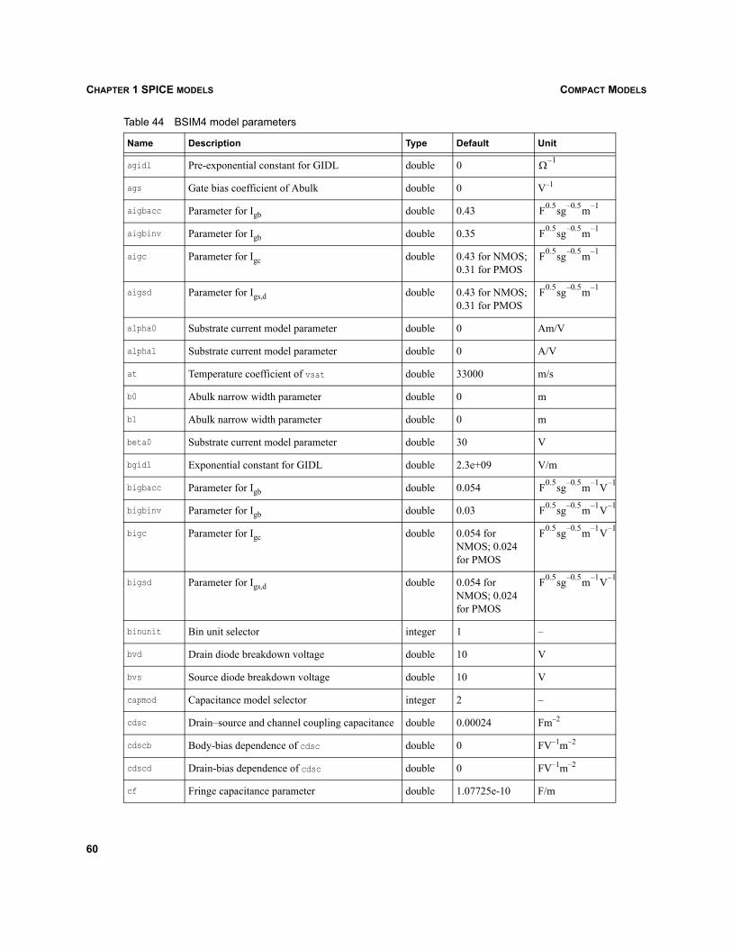
COMPACT MODELSCHAPTER 1 SPICE MODELS
agidl Pre-exponential constant for GIDL double 0
ags Gate bias coefficient of Abulk double 0 V–1
aigbacc Parameter for Igb double 0.43
aigbinv Parameter for Igb double 0.35
aigc Parameter for Igc double 0.43 for NMOS; 0.31 for PMOS
aigsd Parameter for Igs,d double 0.43 for NMOS; 0.31 for PMOS
alpha0 Substrate current model parameter double 0 Am/V
alpha1 Substrate current model parameter double 0 A/V
at Temperature coefficient of vsat double 33000 m/s
b0 Abulk narrow width parameter double 0 m
b1 Abulk narrow width parameter double 0 m
beta0 Substrate current model parameter double 30 V
bgidl Exponential constant for GIDL double 2.3e+09 V/m
bigbacc Parameter for Igb double 0.054
bigbinv Parameter for Igb double 0.03
bigc Parameter for Igc double 0.054 for NMOS; 0.024 for PMOS
bigsd Parameter for Igs,d double 0.054 for NMOS; 0.024 for PMOS
binunit Bin unit selector integer 1 –
bvd Drain diode breakdown voltage double 10 V
bvs Source diode breakdown voltage double 10 V
capmod Capacitance model selector integer 2 –
cdsc Drain–source and channel coupling capacitance double 0.00024 Fm–2
cdscb Body-bias dependence of cdsc double 0 FV–1m–2
cdscd Drain-bias dependence of cdsc double 0 FV–1m–2
cf Fringe capacitance parameter double 1.07725e-10 F/m
Table 44 BSIM4 model parameters
Name Description Type Default Unit
Ω–1
F0.5sg–0.5m–1
F0.5sg–0.5m–1
F0.5sg–0.5m–1
F0.5sg–0.5m–1
F0.5sg–0.5m–1V–1
F0.5sg–0.5m–1V–1
F0.5sg–0.5m–1V–1
F0.5sg–0.5m–1V–1
60

COMPACT MODELS CHAPTER 1 SPICE MODELS
cgbo Gate–bulk overlap capacitance per length double 0 F/m
cgdl New C–V model parameter double 0 F/m
cgdo Gate–drain overlap capacitance per width double 1.03594e-09 F/m
cgidl Parameter for body-bias dependence of GIDL double 0.5 v3
cgsl New C–V model parameter double 0 F/m
cgso Gate–source overlap capacitance per width double 1.03594e-09 F/m
cigbacc Parameter for Igb double 0.075 V–1
cigbinv Parameter for Igb double 0.006 V–1
cigc Parameter for Igc double 0.075 for NMOS;0.03 for PMOS
V–1
cigsd Parameter for Igs,d double 0.075 for NMOS;0.03 for PMOS
V–1
cit Interface state capacitance double 0 Fm–2
cjd Drain bottom junction capacitance per unit area double 0.0005 Fm–2
cjs Source bottom junction capacitance per unit area double 0.0005 Fm–2
cjswd Drain sidewall junction capacitance per unit periphery
double 5e-10 F/m
cjswgd Drain (gate side) sidewall junction capacitance per unit width
double 5e-10 F/m
cjswgs Source (gate side) sidewall junction capacitance per unit width
double 5e-10 F/m
cjsws Source sidewall junction capacitance per unit periphery
double 5e-10 F/m
ckappad Drain–gate overlap C–V parameter double 0.6 V
ckappas Source–gate overlap C–V parameter double 0.6 V
clc Vdsat parameter for C–V model double 1e-07 m
cle Vdsat parameter for C–V model double 0.6 –
delta Effective Vds parameter double 0.01 V
diomod Diode IV model selector integer 1 –
dlc Delta L for C–V model double 0 m
Table 44 BSIM4 model parameters
Name Description Type Default Unit
61

COMPACT MODELSCHAPTER 1 SPICE MODELS
dlcig Delta L for Ig model double 0 m
dmcg Distance of mid-contact to gate edge double 0 m
dmcgt Distance of mid-contact to gate edge in test structures
double 0 m
dmci Distance of mid-contact to isolation double 0 m
dmdg Distance of mid-diffusion to gate edge double 0 m
drout DIBL coefficient of output resistance double 0.56 –
dsub DIBL coefficient in subthreshold region double 0.56 –
dtox Defined as (toxe – toxp) double 0 m
dvt0 Short-channel effect coefficient 0 double 2.2 –
dvt0w Narrow width coefficient 0 double 0 –
dvt1 Short-channel effect coefficient 1 double 0.53 –
dvt1w Narrow width effect coefficient 1 double 5.3e+06 m–1
dvt2 Short-channel effect coefficient 2 double –0.032 V–1
dvt2w Narrow width effect coefficient 2 double –0.032 V–1
dvtp0 First parameter for Vth shift due to pocket double 0 m
dvtp1 Second parameter for Vth shift due to pocket double 0 V–1
dwb Width reduction parameter double 0 –
dwc Delta W for C–V model double 0 m
dwg Width reduction parameter double 0 m/V
dwj Delta W for source–drain junctions double 0 –
ef Flicker noise frequency exponent double 1 –
egidl Fitting parameter for band bending double 0.8 V
eigbinv Parameter for Si band gap for Igbinv double 1.1 V
em Flicker noise parameter double 4.1e+07 –
epsrox Dielectric constant of gate oxide relative to vacuum
double 3.9 –
eta0 Subthreshold region DIBL coefficient double 0.08 –
etab Subthreshold region DIBL coefficient double –0.07 V–1
Table 44 BSIM4 model parameters
Name Description Type Default Unit
62
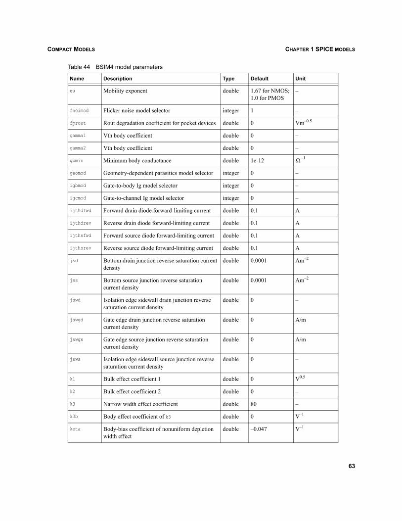
COMPACT MODELS CHAPTER 1 SPICE MODELS
eu Mobility exponent double 1.67 for NMOS; 1.0 for PMOS
–
fnoimod Flicker noise model selector integer 1 –
fprout Rout degradation coefficient for pocket devices double 0 Vm–0.5
gamma1 Vth body coefficient double 0 –
gamma2 Vth body coefficient double 0 –
gbmin Minimum body conductance double 1e-12
geomod Geometry-dependent parasitics model selector integer 0 –
igbmod Gate-to-body Ig model selector integer 0 –
igcmod Gate-to-channel Ig model selector integer 0 –
ijthdfwd Forward drain diode forward-limiting current double 0.1 A
ijthdrev Reverse drain diode forward-limiting current double 0.1 A
ijthsfwd Forward source diode forward-limiting current double 0.1 A
ijthsrev Reverse source diode forward-limiting current double 0.1 A
jsd Bottom drain junction reverse saturation current density
double 0.0001 Am–2
jss Bottom source junction reverse saturation current density
double 0.0001 Am–2
jswd Isolation edge sidewall drain junction reverse saturation current density
double 0 –
jswgd Gate edge drain junction reverse saturation current density
double 0 A/m
jswgs Gate edge source junction reverse saturation current density
double 0 A/m
jsws Isolation edge sidewall source junction reverse saturation current density
double 0 –
k1 Bulk effect coefficient 1 double 0 V0.5
k2 Bulk effect coefficient 2 double 0 –
k3 Narrow width effect coefficient double 80 –
k3b Body effect coefficient of k3 double 0 V–1
keta Body-bias coefficient of nonuniform depletion width effect
double –0.047 V–1
Table 44 BSIM4 model parameters
Name Description Type Default Unit
Ω–1
63
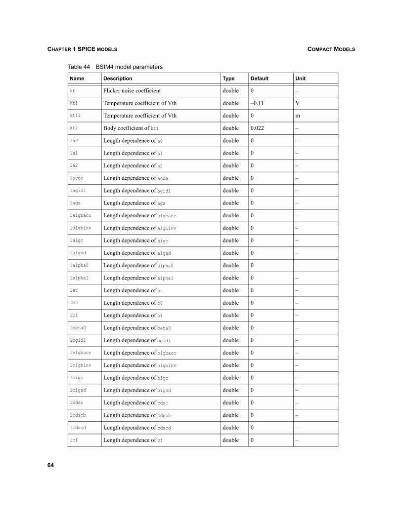
COMPACT MODELSCHAPTER 1 SPICE MODELS
kf Flicker noise coefficient double 0 –
kt1 Temperature coefficient of Vth double –0.11 V
kt1l Temperature coefficient of Vth double 0 m
kt2 Body coefficient of kt1 double 0.022 –
la0 Length dependence of a0 double 0 –
la1 Length dependence of a1 double 0 –
la2 Length dependence of a2 double 0 –
lacde Length dependence of acde double 0 –
lagidl Length dependence of agidl double 0 –
lags Length dependence of ags double 0 –
laigbacc Length dependence of aigbacc double 0 –
laigbinv Length dependence of aigbinv double 0 –
laigc Length dependence of aigc double 0 –
laigsd Length dependence of aigsd double 0 –
lalpha0 Length dependence of alpha0 double 0 –
lalpha1 Length dependence of alpha1 double 0 –
lat Length dependence of at double 0 –
lb0 Length dependence of b0 double 0 –
lb1 Length dependence of b1 double 0 –
lbeta0 Length dependence of beta0 double 0 –
lbgidl Length dependence of bgidl double 0 –
lbigbacc Length dependence of bigbacc double 0 –
lbigbinv Length dependence of bigbinv double 0 –
lbigc Length dependence of bigc double 0 –
lbigsd Length dependence of bigsd double 0 –
lcdsc Length dependence of cdsc double 0 –
lcdscb Length dependence of cdscb double 0 –
lcdscd Length dependence of cdscd double 0 –
lcf Length dependence of cf double 0 –
Table 44 BSIM4 model parameters
Name Description Type Default Unit
64
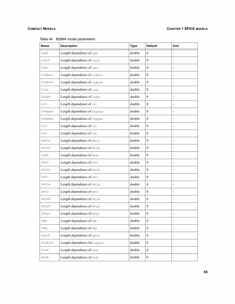
COMPACT MODELS CHAPTER 1 SPICE MODELS
lcgdl Length dependence of cgdl double 0 –
lcgidl Length dependence of cgidl double 0 –
lcgsl Length dependence of cgsl double 0 –
lcigbacc Length dependence of cigbacc double 0 –
lcigbinv Length dependence of cigbinv double 0 –
lcigc Length dependence of cigc double 0 –
lcigsd Length dependence of cigsd double 0 –
lcit Length dependence of cit double 0 –
lckappad Length dependence of ckappad double 0 –
lckappas Length dependence of ckappas double 0 –
lclc Length dependence of clc double 0 –
lcle Length dependence of cle double 0 –
ldelta Length dependence of delta double 0 –
ldrout Length dependence of drout double 0 –
ldsub Length dependence of dsub double 0 –
ldvt0 Length dependence of dvt0 double 0 –
ldvt0w Length dependence of dvt0w double 0 –
ldvt1 Length dependence of dvt1 double 0 –
ldvt1w Length dependence of dvt1w double 0 –
ldvt2 Length dependence of dvt2 double 0 –
ldvt2w Length dependence of dvt2w double 0 –
ldvtp0 Length dependence of dvtp0 double 0 –
ldvtp1 Length dependence of dvtp1 double 0 –
ldwb Length dependence of dwb double 0 –
ldwg Length dependence of dwg double 0 –
legidl Length dependence of egidl double 0 –
leigbinv Length dependence for eigbinv double 0 –
leta0 Length dependence of eta0 double 0 –
letab Length dependence of etab double 0 –
Table 44 BSIM4 model parameters
Name Description Type Default Unit
65

COMPACT MODELSCHAPTER 1 SPICE MODELS
leu Length dependence of eu double 0 –
lfprout Length dependence of pdiblcb double 0 –
lgamma1 Length dependence of gamma1 double 0 –
lgamma2 Length dependence of gamma2 double 0 –
lint Length reduction parameter double 0 m
lk1 Length dependence of k1 double 0 –
lk2 Length dependence of k2 double 0 –
lk3 Length dependence of k3 double 0 –
lk3b Length dependence of k3b double 0 –
lketa Length dependence of keta double 0 –
lkt1 Length dependence of kt1 double 0 –
lkt1l Length dependence of kt1l double 0 –
lkt2 Length dependence of kt2 double 0 –
ll Length reduction parameter double 0
llc Length reduction parameter for CV double 0 –
lln Length reduction parameter double 1 –
llpe0 Length dependence of lpe0 double 0 –
llpeb Length dependence of lpeb double 0 –
lmax Maximum length of model double 1 m
lmin Minimum length of model double 0 –
lminv Length dependence of minv double 0 m
lmoin Length dependence of moin double 0 –
lndep Length dependence of ndep double 0 –
lnfactor Length dependence of nfactor double 0 –
lngate Length dependence of ngate double 0 –
lnigbacc Length dependence of nigbacc double 0 –
lnigbinv Length dependence of nigbinv double 0 –
lnigc Length dependence of nigc double 0 –
lnoff Length dependence of noff double 0 –
Table 44 BSIM4 model parameters
Name Description Type Default Unit
mlln
66

COMPACT MODELS CHAPTER 1 SPICE MODELS
lnsd Length dependence of nsd double 0 –
lnsub Length dependence of nsub double 0 –
lntox Length dependence of ntox double 0 –
lpclm Length dependence of pclm double 0 –
lpdiblc1 Length dependence of pdiblc1 double 0 –
lpdiblc2 Length dependence of pdiblc2 double 0 –
lpdiblcb Length dependence of pdiblcb double 0 –
lpdits Length dependence of pdits double 0 –
lpditsd Length dependence of pditsd double 0 –
lpe0 Equivalent length of pocket region at zero bias double 1.74e-07 m
lpeb Equivalent length of pocket region accounting for body bias
double 0 m
lphin Length dependence of phin double 0 –
lpigcd Length dependence for pigcd double 0 –
lpoxedge Length dependence for poxedge double 0 –
lprt Length dependence of prt double 0 –
lprwb Length dependence of prwb double 0 –
lprwg Length dependence of prwg double 0 –
lpscbe1 Length dependence of pscbe1 double 0 –
lpscbe2 Length dependence of pscbe2 double 0 –
lpvag Length dependence of pvag double 0 –
lrdsw Length dependence of rdsw double 0 –
lrdw Length dependence of rdw double 0 –
lrsw Length dependence of rsw double 0 –
lu0 Length dependence of u0 double 0 –
lua Length dependence of ua double 0 –
lua1 Length dependence of ua1 double 0 –
lub Length dependence of ub double 0 –
lub1 Length dependence of ub1 double 0 –
Table 44 BSIM4 model parameters
Name Description Type Default Unit
67
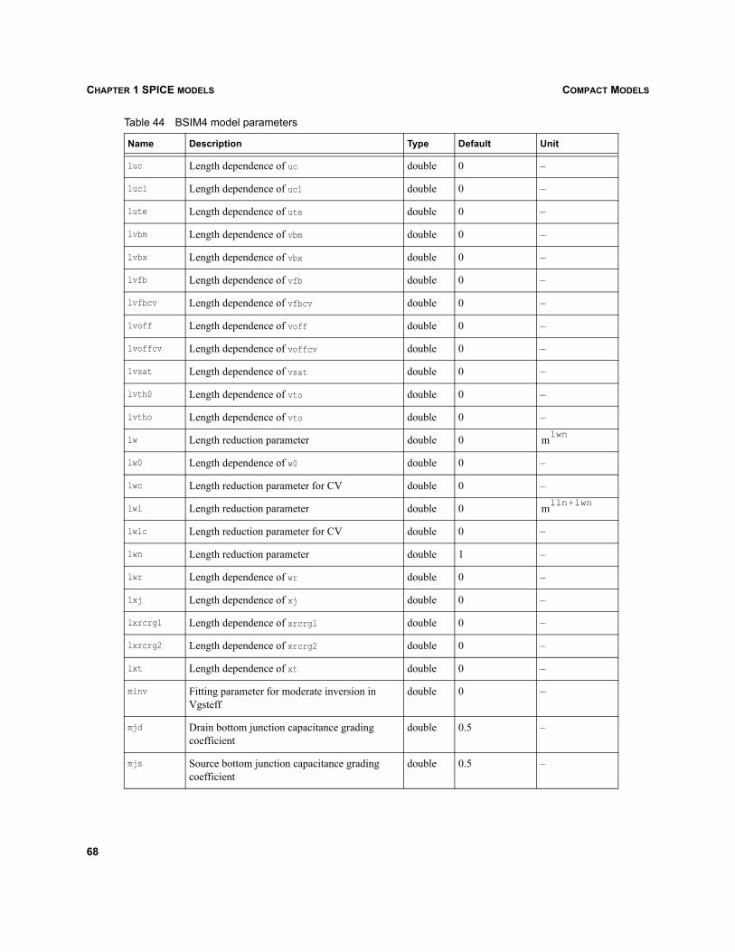
COMPACT MODELSCHAPTER 1 SPICE MODELS
luc Length dependence of uc double 0 –
luc1 Length dependence of uc1 double 0 –
lute Length dependence of ute double 0 –
lvbm Length dependence of vbm double 0 –
lvbx Length dependence of vbx double 0 –
lvfb Length dependence of vfb double 0 –
lvfbcv Length dependence of vfbcv double 0 –
lvoff Length dependence of voff double 0 –
lvoffcv Length dependence of voffcv double 0 –
lvsat Length dependence of vsat double 0 –
lvth0 Length dependence of vto double 0 –
lvtho Length dependence of vto double 0 –
lw Length reduction parameter double 0
lw0 Length dependence of w0 double 0 –
lwc Length reduction parameter for CV double 0 –
lwl Length reduction parameter double 0
lwlc Length reduction parameter for CV double 0 –
lwn Length reduction parameter double 1 –
lwr Length dependence of wr double 0 –
lxj Length dependence of xj double 0 –
lxrcrg1 Length dependence of xrcrg1 double 0 –
lxrcrg2 Length dependence of xrcrg2 double 0 –
lxt Length dependence of xt double 0 –
minv Fitting parameter for moderate inversion in Vgsteff
double 0 –
mjd Drain bottom junction capacitance grading coefficient
double 0.5 –
mjs Source bottom junction capacitance grading coefficient
double 0.5 –
Table 44 BSIM4 model parameters
Name Description Type Default Unit
mlwn
mlln+lwn
68

COMPACT MODELS CHAPTER 1 SPICE MODELS
mjswd Drain sidewall junction capacitance grading coefficient
double 0.33 –
mjswgd Drain (gate side) sidewall junction capacitance grading coefficient
double 0.33 –
mjswgs Source (gate side) sidewall junction capacitance grading coefficient
double 0.33 –
mjsws Source sidewall junction capacitance grading coefficient
double 0.33 –
mobmod Mobility model selector integer 0 –
moin Coefficient for gate bias–dependent surface potential
double 15 –
ndep Channel doping concentration at depletion edge double 1.7e+17 cm–3
nfactor Subthreshold swing coefficient double 1 –
ngate Poly-gate doping concentration double 0 cm–3
ngcon Number of gate contacts double 1 –
nigbacc Parameter for Igbacc slope double 1 –
nigbinv Parameter for Igbinv slope double 3 –
nigc Parameter for Igc slope double 1 –
njd Drain junction emission coefficient double 1 –
njs Source junction emission coefficient double 1 –
noff C–V switch on or off parameter double 1 –
noia Flicker noise parameter double 6.25e+41 NMOS 6.188e+40 PMOS
noib Flicker noise parameter double 3.125e+26 NMOS 1.5e+25 PMOS
noic Flicker noise parameter double 8.75e+09
nsd Source–drain doping concentration double 1e+20 cm–3
nsu Substrate doping concentration double 6e+16 cm–3
ntnoi Thermal noise parameter double 1 –
ntox Exponent for Tox ratio double 1 –
Table 44 BSIM4 model parameters
Name Description Type Default Unit
s1 EF– eV 1– m 3–
s1 EF– eV 1– m 3–
s1 EF– F
69

COMPACT MODELSCHAPTER 1 SPICE MODELS
pa0 Cross-term dependence of a0 double 0 –
pa1 Cross-term dependence of a1 double 0 –
pa2 Cross-term dependence of a2 double 0 –
pacde Cross-term dependence of acde double 0 –
pagidl Cross-term dependence of agidl double 0 –
pags Cross-term dependence of ags double 0 –
paigbacc Cross-term dependence of aigbacc double 0 –
paigbinv Cross-term dependence of aigbinv double 0 –
paigc Cross-term dependence of aigc double 0 –
paigsd Cross-term dependence of aigsd double 0 –
palpha0 Cross-term dependence of alpha0 double 0 –
palpha1 Cross-term dependence of alpha1 double 0 –
paramchk Model parameter checking selector integer 1 –
pat Cross-term dependence of at double 0 –
pb0 Cross-term dependence of b0 double 0 –
pb1 Cross-term dependence of b1 double 0 –
pbd Drain junction built-in potential double 1 V
pbeta0 Cross-term dependence of beta0 double 0 –
pbgidl Cross-term dependence of bgidl double 0 –
pbigbacc Cross-term dependence of bigbacc double 0 –
pbigbinv Cross-term dependence of bigbinv double 0 –
pbigc Cross-term dependence of bigc double 0 –
pbigsd Cross-term dependence of bigsd double 0 –
pbs Source junction built-in potential double 1 V
pbswd Drain sidewall junction capacitance built-in potential
double 1 V
pbswgd Drain (gate side) sidewall junction capacitance built-in potential
double 1 V
pbswgs Source (gate side) sidewall junction capacitance built-in potential
double 1 V
Table 44 BSIM4 model parameters
Name Description Type Default Unit
70

COMPACT MODELS CHAPTER 1 SPICE MODELS
pbsws Source sidewall junction capacitance built-in potential
double 1 V
pcdsc Cross-term dependence of cdsc double 0 –
pcdscb Cross-term dependence of cdscb double 0 –
pcdscd Cross-term dependence of cdscd double 0 –
pcf Cross-term dependence of cf double 0 –
pcgdl Cross-term dependence of cgdl double 0 –
pcgidl Cross-term dependence of cgidl double 0 –
pcgsl Cross-term dependence of cgsl double 0 –
pcigbacc Cross-term dependence of cigbacc double 0 –
pcigbinv Cross-term dependence of cigbinv double 0 –
pcigc Cross-term dependence of cigc double 0 –
pcigsd Cross-term dependence of cigsd double 0 –
pcit Cross-term dependence of cit double 0 –
pckappad Cross-term dependence of ckappad double 0 –
pckappas Cross-term dependence of ckappas double 0 –
pclc Cross-term dependence of clc double 0 –
pcle Cross-term dependence of cle double 0 –
pclm Channel-length modulation coefficient double 1.3 –
pdelta Cross-term dependence of delta double 0 –
pdiblc1 Drain-induced barrier-lowering coefficient double 0.39 –
pdiblc2 Drain-induced barrier-lowering coefficient double 0.0086 –
pdiblcb Body effect on drain-induced barrier lowering double 0 V–1
pdits Coefficient for drain-induced Vth shifts double 0 V–1
pditsd Vds dependence of drain-induced Vth shifts double 0 V–1
pditsl Length dependence of drain-induced Vth shifts double 0 m–1
pdrout Cross-term dependence of drout double 0 –
pdsub Cross-term dependence of dsub double 0 –
pdvt0 Cross-term dependence of dvt0 double 0 –
Table 44 BSIM4 model parameters
Name Description Type Default Unit
71

COMPACT MODELSCHAPTER 1 SPICE MODELS
pdvt0w Cross-term dependence of dvt0w double 0 –
pdvt1 Cross-term dependence of dvt1 double 0 –
pdvt1w Cross-term dependence of dvt1w double 0 –
pdvt2 Cross-term dependence of dvt2 double 0 –
pdvt2w Cross-term dependence of dvt2w double 0 –
pdvtp0 Cross-term dependence of dvtp0 double 0 –
pdvtp1 Cross-term dependence of dvtp1 double 0 –
pdwb Cross-term dependence of dwb double 0 –
pdwg Cross-term dependence of dwg double 0 –
pegidl Cross-term dependence of egidl double 0 –
peigbinv Cross-term dependence for eigbinv double 0 –
permod Pd and Ps model selector integer 1 –
peta0 Cross-term dependence of eta0 double 0 –
petab Cross-term dependence of etab double 0 –
peu Cross-term dependence of eu double 0 –
pfprout Cross-term dependence of pdiblcb double 0 –
pgamma1 Cross-term dependence of gamma1 double 0 –
pgamma2 Cross-term dependence of gamma2 double 0 –
phin Adjusting parameter for surface potential due to nonuniform vertical doping
double 0 V
pigcd Parameter for Igc partition double 1 –
pk1 Cross-term dependence of k1 double 0 –
pk2 Cross-term dependence of k2 double 0 –
pk3 Cross-term dependence of k3 double 0 –
pk3b Cross-term dependence of k3b double 0 –
pketa Cross-term dependence of keta double 0 –
pkt1 Cross-term dependence of kt1 double 0 –
pkt1l Cross-term dependence of kt1l double 0 –
pkt2 Cross-term dependence of kt2 double 0 –
Table 44 BSIM4 model parameters
Name Description Type Default Unit
72

COMPACT MODELS CHAPTER 1 SPICE MODELS
plpe0 Cross-term dependence of lpe0 double 0 –
plpeb Cross-term dependence of lpeb double 0 –
pminv Cross-term dependence of minv double 0 –
pmoin Cross-term dependence of moin double 0 –
pndep Cross-term dependence of ndep double 0 –
pnfactor Cross-term dependence of nfactor double 0 –
pngate Cross-term dependence of ngate double 0 –
pnigbacc Cross-term dependence of nigbacc double 0 –
pnigbinv Cross-term dependence of nigbinv double 0 –
pnigc Cross-term dependence of nigc double 0 –
pnoff Cross-term dependence of noff double 0 –
pnsd Cross-term dependence of nsd double 0 –
pnsub Cross-term dependence of nsub double 0 –
pntox Cross-term dependence of ntox double 0 –
poxedge Factor for the gate edge Tox double 1 –
ppclm Cross-term dependence of pclm double 0 –
ppdiblc1 Cross-term dependence of pdiblc1 double 0 –
ppdiblc2 Cross-term dependence of pdiblc2 double 0 –
ppdiblcb Cross-term dependence of pdiblcb double 0 –
ppdits Cross-term dependence of pdits double 0 –
ppditsd Cross-term dependence of pditsd double 0 –
pphin Cross-term dependence of phin double 0 –
ppigcd Cross-term dependence for pigcd double 0 –
ppoxedge Cross-term dependence for poxedge double 0 –
pprt Cross-term dependence of prt double 0 –
pprwb Cross-term dependence of prwb double 0 –
pprwg Cross-term dependence of prwg double 0 –
ppscbe1 Cross-term dependence of pscbe1 double 0 –
ppscbe2 Cross-term dependence of pscbe2 double 0 –
Table 44 BSIM4 model parameters
Name Description Type Default Unit
73

COMPACT MODELSCHAPTER 1 SPICE MODELS
ppvag Cross-term dependence of pvag double 0 –
prdsw Cross-term dependence of rdsw double 0 –
prdw Cross-term dependence of rdw double 0 –
prsw Cross-term dependence of rsw double 0 –
prt Temperature coefficient of parasitic resistance double 0
prwb Body effect on parasitic resistance double 0 V–0.5
prwg Gate-bias effect on parasitic resistance double 1 V–1
pscbe1 Substrate current body-effect coefficient double 4.24e+08 V/m
pscbe2 Substrate current body-effect coefficient double 1e-05 m/V
pu0 Cross-term dependence of u0 double 0 –
pua Cross-term dependence of ua double 0 –
pua1 Cross-term dependence of ua1 double 0 –
pub Cross-term dependence of ub double 0 –
pub1 Cross-term dependence of ub1 double 0 –
puc Cross-term dependence of uc double 0 –
puc1 Cross-term dependence of uc1 double 0 –
pute Cross-term dependence of ute double 0 –
pvag Gate dependence of output resistance parameter double 0 –
pvbm Cross-term dependence of vbm double 0 –
pvbx Cross-term dependence of vbx double 0 –
pvfb Cross-term dependence of vfb double 0 –
pvfbcv Cross-term dependence of vfbcv double 0 –
pvoff Cross-term dependence of voff double 0 –
pvoffcv Cross-term dependence of voffcv double 0 –
pvsat Cross-term dependence of vsat double 0 –
pvth0 Cross-term dependence of vto double 0 –
pvtho Cross-term dependence of vto double 0 –
pw0 Cross-term dependence of w0 double 0 –
pwr Cross-term dependence of wr double 0 –
Table 44 BSIM4 model parameters
Name Description Type Default Unit
Ω*m
74
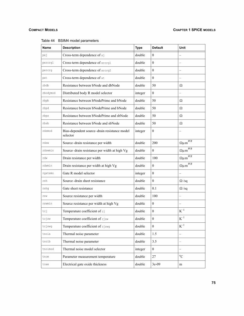
COMPACT MODELS CHAPTER 1 SPICE MODELS
pxj Cross-term dependence of xj double 0 –
pxrcrg1 Cross-term dependence of xrcrg1 double 0 –
pxrcrg Cross-term dependence of xrcrg2 double 0 –
pxt Cross-term dependence of xt double 0 –
rbdb Resistance between bNode and dbNode double 50
rbodymod Distributed body R model selector integer 0 –
rbpb Resistance between bNodePrime and bNode double 50
rbpd Resistance between bNodePrime and bNode double 50
rbps Resistance between bNodePrime and sbNode double 50
rbsb Resistance between bNode and sbNode double 50
rdsmod Bias-dependent source–drain resistance model selector
integer 0 –
rdsw Source–drain resistance per width double 200
rdswmin Source–drain resistance per width at high Vg double 0
rdw Drain resistance per width double 100
rdwmin Drain resistance per width at high Vg double 0
rgatemo Gate R model selector integer 0 –
rsh Source–drain sheet resistance double 0 /sq
rshg Gate sheet resistance double 0.1 /sq
rsw Source resistance per width double 100 –
rswmin Source resistance per width at high Vg double 0 –
tcj Temperature coefficient of cj double 0 K–1
tcjsw Temperature coefficient of cjsw double 0 K–1
tcjswg Temperature coefficient of cjswg double 0 K–1
tnoia Thermal noise parameter double 1.5 –
tnoib Thermal noise parameter double 3.5 –
tnoimod Thermal noise model selector integer 0 –
tnom Parameter measurement temperature double 27 oC
toxe Electrical gate oxide thickness double 3e-09 m
Table 44 BSIM4 model parameters
Name Description Type Default Unit
Ω
Ω
Ω
Ω
Ω
ΩμmWR
ΩμmWR
ΩμmWR
ΩμmWR
Ω
Ω
75

COMPACT MODELSCHAPTER 1 SPICE MODELS
toxm Gate oxide thickness at which parameters are extracted
double 3e-09 m
toxp Physical gate oxide thickness double 3e-09 m
toxref Target tox value double 3e-09 m
tpb Temperature coefficient of pb double 0 V/K
tpbsw Temperature coefficient of pbsw double 0 V/K
tpbswg Temperature coefficient of pbswg double 0 V/K
trnqsmod Transient NQS model selector integer 0 –
u0 Low-field mobility at tnom double 0.067 for NMOS 0.025 for PMOS
ua Linear gate dependence of mobility double 1e-09 MOBMOD=0,11.0e-15 MOBMOD=2
m/V
ua1 Temperature coefficient of ua double 1e-09 m/V
ub Quadratic gate dependence of mobility double 1e-19 m2/V–2
ub1 Temperature coefficient of ub double –1e-18 m2V–2
uc Body-bias dependence of mobility double –4.65e-11 MOBMOD=0,2–0.0465 MOBMOD=1
mV–2
V–1
uc1 Temperature coefficient of uc double –5.6e-11 V–1 for MOBMOD 1; –0.056 for MOBMOD 0, 2
–
ute Temperature coefficient of mobility double –1.5 –
vbm Maximum body voltage double –3 V
vbx Vth transition body voltage double 0V –
version Parameter for model version string 4.1.0 –
vfb Flat-band voltage double 0V –
vfbcv Flat-band voltage parameter for capmod=0 only double –1 V
voff Threshold voltage offset double –0.08 V
voffcv C–V lateral shift parameter double 0 V
voffl Length dependence parameter for Vth offset double 0 mV
Table 44 BSIM4 model parameters
Name Description Type Default Unit
m2 Vs( )–1
76

COMPACT MODELS CHAPTER 1 SPICE MODELS
vsat Saturation velocity at tnom double 80000 m/S
vth0 Threshold voltage double 0.7 NMOS0.7 PMOS
V
vtho Threshold voltage double 0.7 –
w0 Narrow width effect parameter double 2.5e-06 m
wa0 Width dependence of a0 double 0 –
wa1 Width dependence of a1 double 0 –
wa2 Width dependence of a2 double 0 –
wacde Width dependence of acde double 0 –
wagidl Width dependence of agidl double 0 –
wags Width dependence of ags double 0 –
waigbacc Width dependence of aigbacc double 0 –
waigbinv Width dependence of aigbinv double 0 –
waigc Width dependence of aigc double 0 –
waigsd Width dependence of aigsd double 0 –
walpha0 Width dependence of alpha0 double 0 –
walpha1 Width dependence of alpha1 double 0 –
wat Width dependence of at double 0 –
wb0 Width dependence of b0 double 0 –
wb1 Width dependence of b1 double 0 –
wbeta0 Width dependence of beta0 double 0 –
wbgidl Width dependence of bgidl double 0 –
wbigbacc Width dependence of bigbacc double 0 –
wbigbinv Width dependence of bigbinv double 0 –
wbigc Width dependence of bigc double 0 –
wbigsd Width dependence of bigsd double 0 –
wcdsc Width dependence of cdsc double 0 –
wcdscb Width dependence of cdscb double 0 –
wcdscd Width dependence of cdscd double 0 –
Table 44 BSIM4 model parameters
Name Description Type Default Unit
77

COMPACT MODELSCHAPTER 1 SPICE MODELS
wcf Width dependence of cf double 0 –
wcgdl Width dependence of cgdl double 0 –
wcgidl Width dependence of cgidl double 0 –
wcgsl Width dependence of cgsl double 0 –
wcigbacc Width dependence of cigbacc double 0 –
wcigbinv Width dependence of cigbinv double 0 –
wcigc Width dependence of cigc double 0 –
wcigsd Width dependence of cigsd double 0 –
wcit Width dependence of cit double 0 –
wckappad Width dependence of ckappad double 0 –
wckappas Width dependence of ckappas double 0 –
wclc Width dependence of clc double 0 –
wcle Width dependence of cle double 0 –
wdelta Width dependence of delta double 0 –
wdrout Width dependence of drout double 0 –
wdsub Width dependence of dsub double 0 –
wdvt0 Width dependence of dvt0 double 0 –
wdvt0w Width dependence of dvt0w double 0 –
wdvt1 Width dependence of dvt1 double 0 –
wdvt1w Width dependence of dvt1w double 0 –
wdvt2 Width dependence of dvt2 double 0 –
wdvt2w Width dependence of dvt2w double 0 –
wdvtp0 Width dependence of dvtp0 double 0 –
wdvtp1 Width dependence of dvtp1 double 0 –
wdwb Width dependence of dwb double 0 –
wdwg Width dependence of dwg double 0 –
wegidl Width dependence of egidl double 0 –
weigbinv Width dependence of eigbinv double 0 –
weta0 Width dependence of eta0 double 0 –
Table 44 BSIM4 model parameters
Name Description Type Default Unit
78

COMPACT MODELS CHAPTER 1 SPICE MODELS
wetab Width dependence of etab double 0 –
weu Width dependence of eu double 0 –
wfprout Width dependence of pdiblcb double 0 –
wgamma1 Width dependence of gamma1 double 0 –
wgamma2 Width dependence of gamma2 double 0 –
wint Width reduction parameter double 0 m
wk1 Width dependence of k1 double 0 –
wk2 Width dependence of k2 double 0 –
wk3 Width dependence of k3 double 0 –
wk3b Width dependence of k3b double 0 –
wketa Width dependence of keta double 0 –
wkt1 Width dependence of kt1 double 0 –
wkt1l Width dependence of kt1l double 0 –
wkt2 Width dependence of kt2 double 0 –
wl Width reduction parameter double 0
wlc Width reduction parameter for CV double 0 –
wln Width reduction parameter double 1 –
wlpe0 Width dependence of lpe0 double 0 –
wlpeb Width dependence of lpeb double 0 –
wmax Maximum width of model double 1 m
wmin Minimum width of model double 0 m
wminv Width dependence of minv double 0 –
wmoin Width dependence of moin double 0 –
wndep Width dependence of ndep double 0 –
wnfactor Width dependence of nfactor double 0 –
wngate Width dependence of ngate double 0 –
wnigbacc Width dependence of nigbacc double 0 –
wnigbinv Width dependence of nigbinv double 0 –
wnigc Width dependence of nigc double 0 –
Table 44 BSIM4 model parameters
Name Description Type Default Unit
mwln
79

COMPACT MODELSCHAPTER 1 SPICE MODELS
wnoff Width dependence of noff double 0 –
wnsd Width dependence of nsd double 0 –
wnsub Width dependence of nsub double 0 –
wntox Width dependence of ntox double 0 –
wpclm Width dependence of pclm double 0 –
wpdiblc1 Width dependence of pdiblc1 double 0 –
wpdiblc2 Width dependence of pdiblc2 double 0 –
wpdiblcb Width dependence of pdiblcb double 0 –
wpdits Width dependence of pdits double 0 –
wpditsd Width dependence of pditsd double 0 –
wphin Width dependence of phin double 0 –
wpigcd Width dependence of pigcd double 0 –
wpoxedge Width dependence of poxedge double 0 –
wprt Width dependence of prt double 0 –
wprwb Width dependence of prwb double 0 –
wprwg Width dependence of prwg double 0 –
wpscbe1 Width dependence of pscbe1 double 0 –
wpscbe2 Width dependence of pscbe2 double 0 –
wpvag Width dependence of pvag double 0 –
wr Width dependence of rds double 1 –
wrdsw Width dependence of rdsw double 0 –
wrdw Width dependence of rdw double 0 –
wrsw Width dependence of rsw double 0 –
wu0 Width dependence of u0 double 0 –
wua Width dependence of ua double 0 –
wua1 Width dependence of ua1 double 0 –
wub Width dependence of ub double 0 –
wub1 Width dependence of ub1 double 0 –
wuc Width dependence of uc double 0 –
Table 44 BSIM4 model parameters
Name Description Type Default Unit
80

COMPACT MODELS CHAPTER 1 SPICE MODELS
wuc1 Width dependence of uc1 double 0 –
wute Width dependence of ute double 0 –
wvbm Width dependence of vbm double 0 –
wvbx Width dependence of vbx double 0 –
wvfb Width dependence of vfb double 0 –
wvfbcv Width dependence of vfbcv double 0 –
wvoff Width dependence of voff double 0 –
wvoffcv Width dependence of voffcv double 0 –
wvsat Width dependence of vsat double 0 –
wvth0 Width dependence of vto double 0 –
wvtho Width dependence of vto double 0 –
ww Width reduction parameter double 0
ww0 Width dependence of w0 double 0 –
wwc Width reduction parameter for CV double 0 –
wwl Width reduction parameter double 0
wwlc Width reduction parameter for CV double 0 –
wwn Width reduction parameter double 1 –
wwr Width dependence of wr double 0 –
wxj Width dependence of xj double 0 –
wxrcrg1 Width dependence of xrcrg1 double 0 –
wxrcrg2 Width dependence of xrcrg2 double 0 –
wxt Width dependence of xt double 0 –
xgl Variation in Ldrawn double 0 m
xgw Distance from gate contact center to device edge double 0 m
xj Junction depth double 1.5e-07 m
xjbvd Fitting parameter for drain diode breakdown current
double 1 –
xjbvs Fitting parameter for source diode breakdown current
double 1 –
xpart Channel charge partitioning double 0 –
Table 44 BSIM4 model parameters
Name Description Type Default Unit
mwwn
mwwn wln+
81

COMPACT MODELSCHAPTER 1 SPICE MODELS
xrcrg1 First fitting parameter the bias-dependent Rg double 12 –
xrcrg2 Second fitting parameter the bias-dependent Rg double 1 –
xt Doping depth double 1.55e-07 m
xtid Drain junction current temperature exponent double 3 –
xtis Source junction current temperature exponent double 3 –
Table 45 BSIM4 instance parameters
Name Description Type Default Unit
l Length double 5e-06 m
w Width double 5e-06 m
nf Number of fingers double 1 –
min Minimize either D or S integer 0 –
ad Drain area double 0 m2
as Source area double 0 m2
pd Drain perimeter double 0 m
ps Source perimeter double 0 m
nrd Number of squares in drain double 1 –
nrs Number of squares in source double 1 –
off Device is initially off integer false –
rbdb_ins Body resistance double 50
rbsb_ins Body resistance double 50
rbpb_ins Body resistance double 50
rbps_ins Body resistance double 50
rbpd_ins Body resistance double 50
trnqsmod_ins Transient NQS model selector integer 0 –
acnqsmod_ins AC NQS model selector integer 0 –
rbodymod_ins Distributed body R model selector integer 0 –
rgatemod_ins Gate resistance model selector integer 0 –
geomod_ins Geometry-dependent parasitics model selector integer 0 –
Table 44 BSIM4 model parameters
Name Description Type Default Unit
Ω
Ω
Ω
Ω
Ω
82

COMPACT MODELS CHAPTER 1 SPICE MODELS
BSIMPD2.2 MOSFET modelBSIMPD2.2 is a partially depleted (PD) silicon-on-insulator (SOI) MOSFET model.
rgeomod Source–drain resistance and contact model selector integer 0 –
ic[] Vector of D–S, G–S, B–S initial voltages double – V
Device name: B3SOI
Default parameter set name: B3SOI_pset
Electrodes: Drain – External drain nodeGate – Gate nodeSource – External source nodeBackgate – Substrate nodePP – External body contact node (optional)Body – Internal body contact node (optional)Temp – Temperature node (optional)
Internal variables: drain (internal drain voltage, only available if and )source (internal source voltage, only available if and
)
Table 46 BSIMPD2.2 model parameters
Name Description Type Default value Unit
Model control parameters
binunit Bin unit selector integer 1 –
capmod Capacitance model selector integer 2 –
mobmod Mobility model selector integer 1 –
noimod Noise model selector integer 1 –
paramchk Model parameter checking selector integer 0 –
shmod Self-heating mode selector: 0 – no self-heating; 1 – self-heating
integer 0 –
version Parameter for model version double 2.0 –
Process parameters
gamma1 Vth body coefficient double 0.0 V1/2
gamma2 Vth body coefficient double 0.0 V1/2
Table 45 BSIM4 instance parameters
Name Description Type Default Unit
rsh 0> nrd 0>
rsh 0>
nrs 0>
83

COMPACT MODELSCHAPTER 1 SPICE MODELS
nch Channel doping concentration double 1.7e17 cm–3
ngate Poly-silicon gate doping concentration double 0.0 cm–3
nsub Substrate doping concentration double 6.0e16 cm–3
tbox Buried oxide thickness double 3.0e-7 m
tox Gate oxide thickness double 1.0e-8 m
tsi Silicon film thickness double 1.0e-7 m
vbm Maximum body voltage double 0.0 V
vbx Vth transition body voltage double 0.0 V
xj Source–drain junction depth double tsi m
xt Doping depth double 1.55e-7 m
DC parameters
vth0 Threshold voltage at Vbs=0 for long and wide device
double 0.7 (NMOS)–0.7 (PMOS)
V
k1 First-order body-effect coefficient double 0.6 V1/2
k1w1 First body-effect width-dependent parameter double 0.0 m
k1w2 Second body-effect width-dependent parameter
double 0.0 m
k2 Second-order body-effect coefficient double 0.0 –
k3 Narrow width coefficient double 80.0 –
k3b Body effect coefficient of k3 double 0.0 V–1
w0 Narrow width parameter double 2.5e-6 m
kb1 Backgate body charge coefficient double 1 –
nlx Lateral nonuniform doping parameter double 1.74e-7 m
dvt0 First coefficient of short-channel effect on Vth double 2.2 –
dvt1 Second coefficient of short-channel effect on Vth
double 0.53 –
dvt2 Body-bias coefficient of short-channel effect on Vth
double –0.032 V-1
dvt0w First coefficient of narrow width effect on Vth for small channel length
double 0.0 –
Table 46 BSIMPD2.2 model parameters
Name Description Type Default value Unit
84

COMPACT MODELS CHAPTER 1 SPICE MODELS
dvt1w Second coefficient of narrow width effect on Vth for small channel length
double 5.3e6 m–1
dvt2w Body-bias coefficient of narrow width effect for small channel length
double –0.032 V–1
u0 Low-field mobility at Temp=Tnom double 0.067 (NMOS)0.025 (PMOS)
m2/(Vs)
ua Coefficient of first-order mobility degradation due to vertical field
double 2.25e-9 m/V
ub Coefficient of second-order mobility degradation due to vertical field
double 5.87e-19 m2/V2
uc Coefficient of mobility degradation due to body-bias effect
double –0.0465 mobmod=3;–4.65e-11 mobmod=1,2
V-1
m/V2
vsat Saturation velocity at Temp=Tnom double 8.0e4 m/s
a0 Coefficient of channel-length dependence of bulk charge effect
double 1.0 –
ags Coefficient of Vgs dependence of bulk charge effect
double 0.0 V-1
b0 Bulk charge effect coefficient for channel width
double 0.0 m
b1 Bulk charge effect width offset double 0.0 m
keta Body-bias coefficient of bulk charge effect double –0.6 V–1
ketas Surface potential adjustment for bulk charge effect
double 0.0 V
a1 First nonsaturation effect parameter double 0.0 V–1
a2 Second nonsaturation factor double 1.0 –
rdsw Parasitic resistance per unit width double 100.0
prwb Body-bias dependence of rdsw double 0.0 V–1/2
prwg Gate-bias dependence of rdsw double 0.0 V–1
wr Channel-width dependence parameter of rdsw double 1.0 –
nfactor Subthreshold swing factor double 1.0 –
wint Width offset fitting parameter from I-V without bias
double 0.0 m
lint Length offset fitting parameter from I-V without bias
double 0.0 m
Table 46 BSIMPD2.2 model parameters
Name Description Type Default value Unit
Ω μm( )wr
85
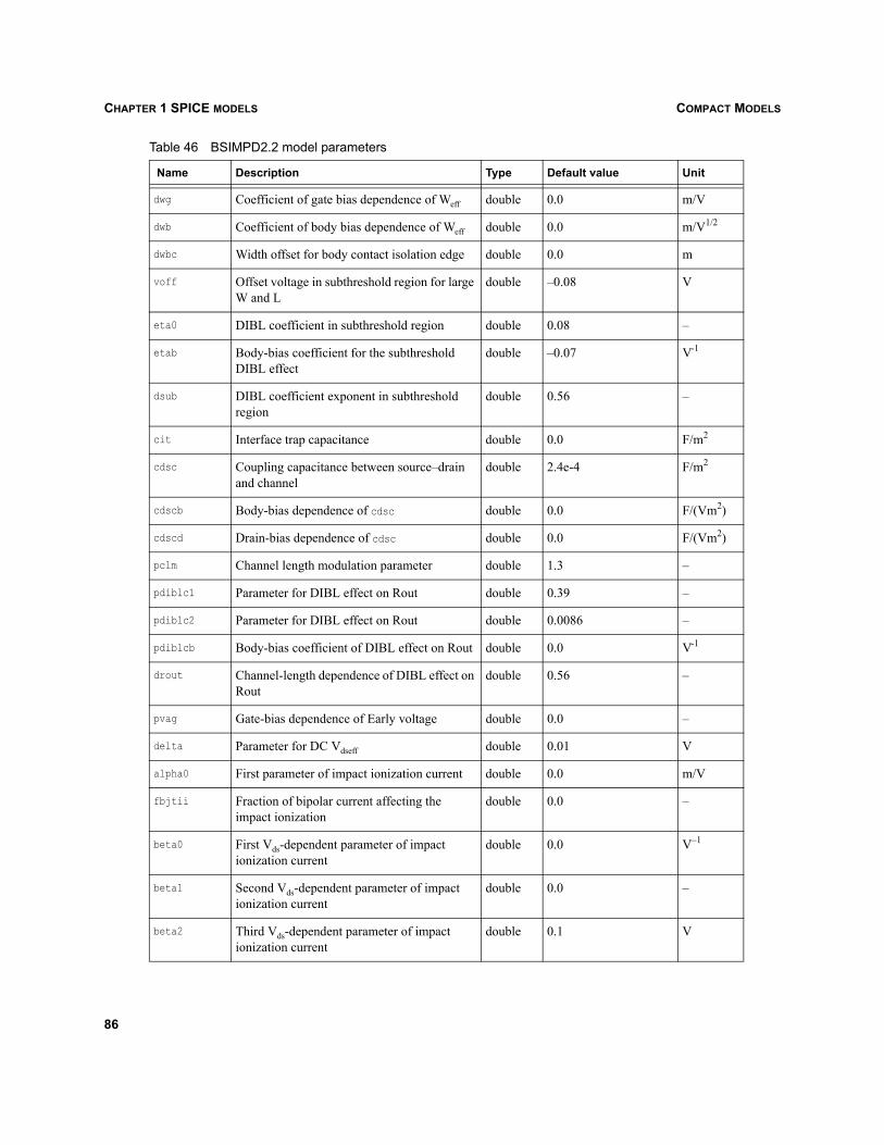
COMPACT MODELSCHAPTER 1 SPICE MODELS
dwg Coefficient of gate bias dependence of Weff double 0.0 m/V
dwb Coefficient of body bias dependence of Weff double 0.0 m/V1/2
dwbc Width offset for body contact isolation edge double 0.0 m
voff Offset voltage in subthreshold region for large W and L
double –0.08 V
eta0 DIBL coefficient in subthreshold region double 0.08 –
etab Body-bias coefficient for the subthreshold DIBL effect
double –0.07 V-1
dsub DIBL coefficient exponent in subthreshold region
double 0.56 –
cit Interface trap capacitance double 0.0 F/m2
cdsc Coupling capacitance between source–drain and channel
double 2.4e-4 F/m2
cdscb Body-bias dependence of cdsc double 0.0 F/(Vm2)
cdscd Drain-bias dependence of cdsc double 0.0 F/(Vm2)
pclm Channel length modulation parameter double 1.3 –
pdiblc1 Parameter for DIBL effect on Rout double 0.39 –
pdiblc2 Parameter for DIBL effect on Rout double 0.0086 –
pdiblcb Body-bias coefficient of DIBL effect on Rout double 0.0 V-1
drout Channel-length dependence of DIBL effect on Rout
double 0.56 –
pvag Gate-bias dependence of Early voltage double 0.0 –
delta Parameter for DC Vdseff double 0.01 V
alpha0 First parameter of impact ionization current double 0.0 m/V
fbjtii Fraction of bipolar current affecting the impact ionization
double 0.0 –
beta0 First Vds-dependent parameter of impact ionization current
double 0.0 V–1
beta1 Second Vds-dependent parameter of impact ionization current
double 0.0 –
beta2 Third Vds-dependent parameter of impact ionization current
double 0.1 V
Table 46 BSIMPD2.2 model parameters
Name Description Type Default value Unit
86

COMPACT MODELS CHAPTER 1 SPICE MODELS
vdsatii0 Nominal drain saturation voltage at threshold for impact ionization current
double 0.9 V
tii Temperature-dependent parameter for impact ionization current
double 0.0 –
lii Channel length–dependent parameter at threshold for impact ionization current
double 0.0 m
esatii Saturation electric field for impact ionization double 1.0e7 V/m
sii0 First Vgs-dependent parameter for impact ionization current
double 0.5 V–1
sii1 Second Vgs-dependent parameter for impact ionization current
double 0.1 V–1
sii2 Third Vgs-dependent parameter for impact ionization current
double 0.0 V–1
siid Vds-dependent parameter of drain saturation voltage for impact ionization current
double 0.0 V-1
agidl GIDL constant double 0.0
bgidl GIDL exponential coefficient double 0.0 V/m
ngidl GIDL Vds enhancement coefficient double 1.2 V
ntun Reverse tunneling nonideality factor double 10.0 –
ndiode Diode nonideality factor double 1.0 –
nrecf0 Recombination nonideality factor at forward bias
double 2.0 –
nrecr0 Recombination nonideality factor at reverse bias
double 10.0 –
isbjt BJT injection saturation current double 1.0e-6 A/m2
isdif Body to source–drain injection saturation current
double 0.0 A/m2
isrec Recombination in depletion saturation current double 1.0e-5 A/m2
istun Reverse tunneling saturation current double 0.0 A/m2
ln Electron–hole diffusion length double 2.0e-6 m
vrec0 Voltage-dependent parameter for recombination current
double 0.0 V
vtun0 Voltage-dependent parameter for tunneling current
double 0.0 V
Table 46 BSIMPD2.2 model parameters
Name Description Type Default value Unit
Ω 1–
87

COMPACT MODELSCHAPTER 1 SPICE MODELS
nbjt Power coefficient of channel length–dependency for bipolar current
double 1.0 –
lbjt0 Reference channel length for bipolar current double 2.0e-7 m
vabjt Early voltage for bipolar current double 10.0 V
aely Channel length–dependency of Early voltage for bipolar current
double 0.0 V/m
ahli High-level injection parameter for bipolar current
double 0.0 –
rbody Intrinsic body contact sheet resistance double 0.0 /sq
rbsh Extrinsic body contact sheet resistance double 0.0 /sq
rsh Source–drain sheet resistance double 0.0 /sq
rhalo Body halo sheet resistance double 1.0e15 /m
Gate-to-body tunneling parameters
igmod Gate current model selector double 0 –
toxqm Oxide thickness for Igb calculation double tox m
ntox Power term of gate current double 1.0 –
toxref Target oxide thickness double 2.5e-9 m
ebg Effective band gap in gate current calculation double 1.2 V
alphagb1 First Vox-dependent parameter for gate current in inversion
double 0.35 V–1
betagb1 Second Vox-dependent parameter for gate current in inversion
double 0.03 V–2
vgb1 Third Vox-dependent parameter for gate current in inversion
double 300.0 V
vevb Vaux parameter for valence band electron tunneling
double 0.075 –
alphagb2 First Vox-dependent parameter for gate current in accumulation
double 0.43 V–1
betagb2 Second Vox-dependent parameter for gate current in accumulation
double 0.05 V–2
vgb2 Third Vox-dependent parameter for gate current in accumulation
double 17.0 V
Table 46 BSIMPD2.2 model parameters
Name Description Type Default value Unit
Ω
Ω
Ω
Ω
88
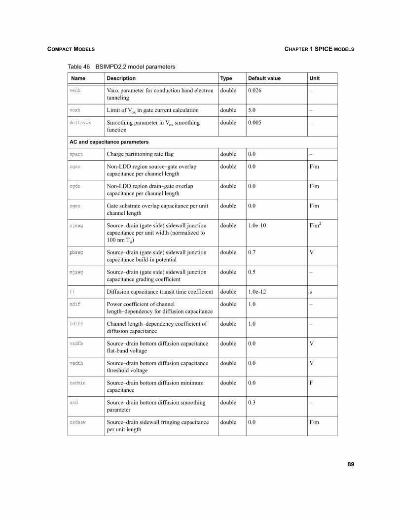
COMPACT MODELS CHAPTER 1 SPICE MODELS
vecb Vaux parameter for conduction band electron tunneling
double 0.026 –
voxh Limit of Vox in gate current calculation double 5.0 –
deltavox Smoothing parameter in Vox smoothing function
double 0.005 –
AC and capacitance parameters
xpart Charge partitioning rate flag double 0.0 –
cgso Non-LDD region source–gate overlap capacitance per channel length
double 0.0 F/m
cgdo Non-LDD region drain–gate overlap capacitance per channel length
double 0.0 F/m
cgeo Gate substrate overlap capacitance per unit channel length
double 0.0 F/m
cjswg Source–drain (gate side) sidewall junction capacitance per unit width (normalized to 100 nm Tsi)
double 1.0e-10 F/m2
pbswg Source–drain (gate side) sidewall junction capacitance build-in potential
double 0.7 V
mjswg Source–drain (gate side) sidewall junction capacitance grading coefficient
double 0.5 –
tt Diffusion capacitance transit time coefficient double 1.0e-12 s
ndif Power coefficient of channel length–dependency for diffusion capacitance
double 1.0 –
ldif0 Channel length–dependency coefficient of diffusion capacitance
double 1.0 –
vsdfb Source–drain bottom diffusion capacitance flat-band voltage
double 0.0 V
vsdth Source–drain bottom diffusion capacitance threshold voltage
double 0.0 V
csdmin Source–drain bottom diffusion minimum capacitance
double 0.0 F
asd Source–drain bottom diffusion smoothing parameter
double 0.3 –
csdesw Source–drain sidewall fringing capacitance per unit length
double 0.0 F/m
Table 46 BSIMPD2.2 model parameters
Name Description Type Default value Unit
89

COMPACT MODELSCHAPTER 1 SPICE MODELS
cgsl Light-doped source–gate region overlap capacitance
double 0.0 F/m
cgdl Light-doped drain–gate region overlap capacitance
double 0.0 F/m
ckappa Coefficient of bias-dependent for light-doped region overlap capacitance
double 0.6 –
cf Gate to source–drain fringing field capacitance
double 0.0 F/m
clc Constant term for short-channel model double 1.0e-8 m
cle Exponential term for short-channel model double 0.0 –
dlc Length offset fitting parameter for gate charge double 0.0 m
dlcb Length offset fitting parameter for body charge
double 0.0 m
dlbg Length offset fitting parameter for backgate charge
double 0.0 m
dwc Width offset fitting parameter for C–V double 0.0 m
delvt Threshold voltage adjust for C–V double 0.0 V
fbody Scaling factor for body charge double 1.0 –
acde Exponential coefficient for charge thickness in capmod=3 for accumulation and depletion regions
double 1.0 m/V
moin Coefficient for gate bias–dependent surface potential
double 15.0 V0.5
Temperature parameters
tnom Temperature at which parameters are extracted
double 27 oC
ute Temperature coefficient of mobility double –1.5 –
kt1 Temperature coefficient for Vth double –0.11 V
kt1l Channel-length dependence of temperature coefficient for Vth
double 0.0 Vm
kt2 Body-bias coefficient of Vth temperature effect
double 0.022 –
ua1 Temperature coefficient of ua double 4.31e-9 m/V
ub1 Temperature coefficient of ub double –7.61e-18 (m/V)2
Table 46 BSIMPD2.2 model parameters
Name Description Type Default value Unit
90

COMPACT MODELS CHAPTER 1 SPICE MODELS
uc1 Temperature coefficient of uc double –0.056 mobmod=3–0.056e-9 mobmod=1,2
V–1
m/V2
at Temperature coefficient of vsat double 3.3e4 m/s
tcjswg Temperature coefficient of cjswg double 0.0 1/oC
tpbswg Temperature coefficient of pbswg double 0.0 V/oC
prt Temperature coefficient of rdsw double 0.0 -m
cth0 Normalized thermal capacity double 0.0 Ws/moC
rth0 Normalized thermal resistance double 0.0 moC/W
ntrecf Temperature coefficient for nrecf double 0.0 –
ntrecr Temperature coefficient for nrecr double 0.0 –
xbjt Power dependence of jbjt on temperature double 1.0 –
xdif Power dependence of jdif on temperature double 1.0 –
xrec Power dependence of jrec on temperature double 1.0 –
xtun Power dependence of jtun on temperature double 0.0 –
wth0 Minimum width for thermal resistance calculation
double 0.0 m
dW and dL parameters
ll Coefficient of length dependence for length offset
double 0.0 mlln
lln Power of length dependence for length offset double 1.0 –
lw Coefficient of width dependence for length offset
double 0.0 mlwn
lwn Power of width dependence for length offset double 1.0 –
lwl Coefficient of length and width cross-term dependence for length offset
double 0.0 mlwn+lln
wl Coefficient of length dependence for width offset
double 0.0 mwln
wln Power of length dependence of width offset double 1.0 –
ww Coefficient of width dependence for width offset
double 0.0 mwwn
wwn Power of width dependence of width offset double 1.0 –
Table 46 BSIMPD2.2 model parameters
Name Description Type Default value Unit
Ω
91

COMPACT MODELSCHAPTER 1 SPICE MODELS
wwl Coefficient of length and width cross-term dependence for width offset
double 0.0 mwwn+wln
Noise parameters
af Flicker noise exponent double 1.0 –
ef Flicker noise frequency exponent double 1.0 –
em Flicker noise parameter double 4.1e7 V/m
kf Flicker noise coefficient double 0.0 –
noia Flicker noise parameter double 1e20 NMOS9.9e18 PMOS
–
noib Flicker noise parameter double 5e4 NMOS2.4e3 PMOS
–
noic Flicker noise parameter double –1.4e-12 NMOS1.4e-12 PMOS
–
noif Floating body excess noise ideality factor double 1.0 –
Length dependence
lnch Length dependence of nch double 0.0 –
lnsub Length dependence of nsub double 0.0 –
lngate Length dependence of ngate double 0.0 –
lvth0 Length dependence of vto double 0.0 –
lk1 Length dependence of k1 double 0.0 –
lk1w1 Length dependence of k1w1 double 0.0 –
lk1w2 Length dependence of k1w2 double 0.0 –
lk2 Length dependence of k2 double 0.0 –
lk3 Length dependence of k3 double 0.0 –
lk3b Length dependence of k3b double 0.0 –
lkb1 Length dependence of kb1 double 0.0 –
lw0 Length dependence of w0 double 0.0 –
lnlx Length dependence of nlx double 0.0 –
ldvt0 Length dependence of dvt0 double 0.0 –
ldvt1 Length dependence of dvt1 double 0.0 –
Table 46 BSIMPD2.2 model parameters
Name Description Type Default value Unit
92

COMPACT MODELS CHAPTER 1 SPICE MODELS
ldvt2 Length dependence of dvt2 double 0.0 –
ldvt0w Length dependence of dvt0w double 0.0 –
ldvt1w Length dependence of dvt1w double 0.0 –
ldvt2w Length dependence of dvt2w double 0.0 –
lu0 Length dependence of u0 double 0.0 –
lua Length dependence of ua double 0.0 –
lub Length dependence of ub double 0.0 –
luc Length dependence of uc double 0.0 –
lvsat Length dependence of vsat double 0.0 –
la0 Length dependence of a0 double 0.0 –
lags Length dependence of ags double 0.0 –
lb0 Length dependence of b0 double 0.0 –
lb1 Length dependence of b1 double 0.0 –
lketa Length dependence of keta double 0.0 –
lketas Length dependence of ketas double 0.0 –
la1 Length dependence of a1 double 0.0 –
la2 Length dependence of a2 double 0.0 –
lrdsw Length dependence of rdsw double 0.0 –
lprwb Length dependence of prwb double 0.0 –
lprwg Length dependence of prwg double 0.0 –
lwr Length dependence of wr double 0.0 –
lnfactor Length dependence of nfactor double 0.0 –
ldwg Length dependence of dwg double 0.0 –
ldwb Length dependence of dwb double 0.0 –
lvoff Length dependence of voff double 0.0 –
leta0 Length dependence of eta0 double 0.0 –
letab Length dependence of etab double 0.0 –
ldsub Length dependence of dsub double 0.0 –
lcit Length dependence of cit double 0.0 –
Table 46 BSIMPD2.2 model parameters
Name Description Type Default value Unit
93

COMPACT MODELSCHAPTER 1 SPICE MODELS
lcdsc Length dependence of cdsc double 0.0 –
lcdscb Length dependence of cdscb double 0.0 –
lcdscd Length dependence of cdscd double 0.0 –
lpclm Length dependence of pclm double 0.0 –
lpdiblc1 Length dependence of pdiblc1 double 0.0 –
lpdiblc2 Length dependence of pdiblc2 double 0.0 –
lpdiblcb Length dependence of pdiblcb double 0.0 –
ldrout Length dependence of drout double 0.0 –
lpvag Length dependence of pvag double 0.0 –
ldelta Length dependence of delta double 0.0 –
lalpha0 Length dependence of alpha0 double 0.0 –
lfbjtii Length dependence of fbjtii double 0.0 –
lbeta0 Length dependence of beta0 double 0.0 –
lbeta1 Length dependence of beta1 double 0.0 –
lbeta2 Length dependence of beta2 double 0.0 –
lvdsatii0 Length dependence of vdsatii0 double 0.0 –
llii Length dependence of lii double 0.0 –
lesatii Length dependence of esatii double 0.0 –
lsii0 Length dependence of sii0 double 0.0 –
lsii1 Length dependence of sii1 double 0.0 –
lsii2 Length dependence of sii2 double 0.0 –
lsiid Length dependence of siid double 0.0 –
lagidl Length dependence of agidl double 0.0 –
lbgidl Length dependence of bgidl double 0.0 –
lngidl Length dependence of ngidl double 0.0 –
lntun Length dependence of ntun double 0.0 –
lndiode Length dependence of ndiode double 0.0 –
lnrecf0 Length dependence of nrecf0 double 0.0 –
lnrecr0 Length dependence of nrecr0 double 0.0 –
Table 46 BSIMPD2.2 model parameters
Name Description Type Default value Unit
94

COMPACT MODELS CHAPTER 1 SPICE MODELS
lisbjt Length dependence of isbjt double 0.0 –
lisdif Length dependence of isdif double 0.0 –
lisrec Length dependence of isrec double 0.0 –
listun Length dependence of istun double 0.0 –
lvrec0 Length dependence of vrec0 double 0.0 –
lvtun0 Length dependence of vtun0 double 0.0 –
lnbjt Length dependence of nbjt double 0.0 –
llbjt0 Length dependence of lbjt0 double 0.0 –
lvabjt Length dependence of vabjt double 0.0 –
laely Length dependence of aely double 0.0 –
lahli Length dependence of ahli double 0.0 –
lvsdfb Length dependence of vsdfb double 0.0 –
lvsdth Length dependence of vsdth double 0.0 –
ldelvt Length dependence of delvt double 0.0 –
lacde Length dependence of acde double 0.0 –
lmoin Length dependence of amoin double 0.0 –
Width dependence
wnch Width dependence of nch double 0.0 –
wnsub Width dependence of nsub double 0.0 –
wngate Width dependence of ngate double 0.0 –
wvth0 Width dependence of vto double 0.0 –
wk1 Width dependence of k1 double 0.0 –
wk1w1 Width dependence of k1w1 double 0.0 –
wk1w2 Width dependence of k1w2 double 0.0 –
wk2 Width dependence of k2 double 0.0 –
wk3 Width dependence of k3 double 0.0 –
wk3b Width dependence of k3b double 0.0 –
wkb1 Width dependence of kb1 double 0.0 –
ww0 Width dependence of w0 double 0.0 –
Table 46 BSIMPD2.2 model parameters
Name Description Type Default value Unit
95

COMPACT MODELSCHAPTER 1 SPICE MODELS
wnlx Width dependence of nlx double 0.0 –
wdvt0 Width dependence of dvt0 double 0.0 –
wdvt1 Width dependence of dvt1 double 0.0 –
wdvt2 Width dependence of dvt2 double 0.0 –
wdvt0w Width dependence of dvt0w double 0.0 –
wdvt1w Width dependence of dvt1w double 0.0 –
wdvt2w Width dependence of dvt2w double 0.0 –
wu0 Width dependence of u0 double 0.0 –
wua Width dependence of ua double 0.0 –
wub Width dependence of ub double 0.0 –
wuc Width dependence of uc double 0.0 –
wvsat Width dependence of vsat double 0.0 –
wa0 Width dependence of a0 double 0.0 –
wags Width dependence of ags double 0.0 –
wb0 Width dependence of b0 double 0.0 –
wb1 Width dependence of b1 double 0.0 –
wketa Width dependence of keta double 0.0 –
wketas Width dependence of ketas double 0.0 –
wa1 Width dependence of a1 double 0.0 –
wa2 Width dependence of a2 double 0.0 –
wrdsw Width dependence of rdsw double 0.0 –
wprwb Width dependence of prwb double 0.0 –
wprwg Width dependence of prwg double 0.0 –
wwr Width dependence of wr double 0.0 –
wnfactor Width dependence of nfactor double 0.0 –
wdwg Width dependence of dwg double 0.0 –
wdwb Width dependence of dwb double 0.0 –
wvoff Width dependence of voff double 0.0 –
weta0 Width dependence of eta0 double 0.0 –
Table 46 BSIMPD2.2 model parameters
Name Description Type Default value Unit
96

COMPACT MODELS CHAPTER 1 SPICE MODELS
wetab Width dependence of etab double 0.0 –
wdsub Width dependence of dsub double 0.0 –
wcit Width dependence of cit double 0.0 –
wcdsc Width dependence of cdsc double 0.0 –
wcdscb Width dependence of cdscb double 0.0 –
wcdscd Width dependence of cdscd double 0.0 –
wpclm Width dependence of pclm double 0.0 –
wpdiblc1 Width dependence of pdiblc1 double 0.0 –
wpdiblc2 Width dependence of pdiblc2 double 0.0 –
wpdiblcb Width dependence of pdiblcb double 0.0 –
wdrout Width dependence of drout double 0.0 –
wpvag Width dependence of pvag double 0.0 –
wdelta Width dependence of delta double 0.0 –
walpha0 Width dependence of alpha0 double 0.0 –
wfbjtii Width dependence of fbjtii double 0.0 –
wbeta0 Width dependence of beta0 double 0.0 –
wbeta1 Width dependence of beta1 double 0.0 –
wbeta2 Width dependence of beta2 double 0.0 –
wvdsatii0 Width dependence of vdsatii0 double 0.0 –
wlii Width dependence of lii double 0.0 –
wesatii Width dependence of esatii double 0.0 –
wsii0 Width dependence of sii0 double 0.0 –
wsii1 Width dependence of sii1 double 0.0 –
wsii2 Width dependence of sii2 double 0.0 –
wsiid Width dependence of siid double 0.0 –
wagidl Width dependence of agidl double 0.0 –
wbgidl Width dependence of bgidl double 0.0 –
wngidl Width dependence of ngidl double 0.0 –
wntun Width dependence of ntun double 0.0 –
Table 46 BSIMPD2.2 model parameters
Name Description Type Default value Unit
97

COMPACT MODELSCHAPTER 1 SPICE MODELS
wndiode Width dependence of ndiode double 0.0 –
wnrecf0 Width dependence of nrecf0 double 0.0 –
wnrecr0 Width dependence of nrecr0 double 0.0 –
wisbjt Width dependence of isbjt double 0.0 –
wisdif Width dependence of isdif double 0.0 –
wisrec Width dependence of isrec double 0.0 –
wistun Width dependence of istun double 0.0 –
wvrec0 Width dependence of vrec0 double 0.0 –
wvtun0 Width dependence of vtun0 double 0.0 –
wnbjt Width dependence of nbjt double 0.0 –
wlbjt0 Width dependence of lbjt0 double 0.0 –
wvabjt Width dependence of vabjt double 0.0 –
waely Width dependence of aely double 0.0 –
wahli Width dependence of ahli double 0.0 –
wvsdfb Width dependence of vsdfb double 0.0 –
wvsdth Width dependence of vsdth double 0.0 –
wdelvt Width dependence of delvt double 0.0 –
wacde Width dependence of acde double 0.0 –
wmoin Width dependence of amoin double 0.0 –
Cross-term dependence
pnch Cross-term dependence of nch double 0.0 –
pnsub Cross-term dependence of nsub double 0.0 –
pngate Cross-term dependence of ngate double 0.0 –
pvth0 Cross-term dependence of vto double 0.0 –
pk1 Cross-term dependence of k1 double 0.0 –
pk1w1 Cross-term dependence of k1w1 double 0.0 –
pk1w2 Cross-term dependence of k1w2 double 0.0 –
pk2 Cross-term dependence of k2 double 0.0 –
pk3 Cross-term dependence of k3 double 0.0 –
Table 46 BSIMPD2.2 model parameters
Name Description Type Default value Unit
98

COMPACT MODELS CHAPTER 1 SPICE MODELS
pk3b Cross-term dependence of k3b double 0.0 –
pkb1 Cross-term dependence of kb1 double 0.0 –
pw0 Cross-term dependence of w0 double 0.0 –
pnlx Cross-term dependence of nlx double 0.0 –
pdvt0 Cross-term dependence of dvt0 double 0.0 –
pdvt1 Cross-term dependence of dvt1 double 0.0 –
pdvt2 Cross-term dependence of dvt2 double 0.0 –
pdvt0w Cross-term dependence of dvt0w double 0.0 –
pdvt1w Cross-term dependence of dvt1w double 0.0 –
pdvt2w Cross-term dependence of dvt2w double 0.0 –
pu0 Cross-term dependence of u0 double 0.0 –
pua Cross-term dependence of ua double 0.0 –
pub Cross-term dependence of ub double 0.0 –
puc Cross-term dependence of uc double 0.0 –
pvsat Cross-term dependence of vsat double 0.0 –
pa0 Cross-term dependence of a0 double 0.0 –
pags Cross-term dependence of ags double 0.0 –
pb0 Cross-term dependence of b0 double 0.0 –
pb1 Cross-term dependence of b1 double 0.0 –
pketa Cross-term dependence of keta double 0.0 –
pketas Cross-term dependence of ketas double 0.0 –
pa1 Cross-term dependence of a1 double 0.0 –
pa2 Cross-term dependence of a2 double 0.0 –
prdsw Cross-term dependence of rdsw double 0.0 –
pprwb Cross-term dependence of prwb double 0.0 –
pprwg Cross-term dependence of prwg double 0.0 –
pwr Cross-term dependence of wr double 0.0 –
pnfactor Cross-term dependence of nfactor double 0.0 –
pdwg Cross-term dependence of dwg double 0.0 –
Table 46 BSIMPD2.2 model parameters
Name Description Type Default value Unit
99

COMPACT MODELSCHAPTER 1 SPICE MODELS
pdwb Cross-term dependence of dwb double 0.0 –
pvoff Cross-term dependence of voff double 0.0 –
peta0 Cross-term dependence of eta0 double 0.0 –
petab Cross-term dependence of etab double 0.0 –
pdsub Cross-term dependence of dsub double 0.0 –
pcit Cross-term dependence of cit double 0.0 –
pcdsc Cross-term dependence of cdsc double 0.0 –
pcdscb Cross-term dependence of cdscb double 0.0 –
pcdscd Cross-term dependence of cdscd double 0.0 –
ppclm Cross-term dependence of pclm double 0.0 –
ppdiblc1 Cross-term dependence of pdiblc1 double 0.0 –
ppdiblc2 Cross-term dependence of pdiblc2 double 0.0 –
ppdiblcb Cross-term dependence of pdiblcb double 0.0 –
pdrout Cross-term dependence of drout double 0.0 –
ppvag Cross-term dependence of pvag double 0.0 –
pdelta Cross-term dependence of delta double 0.0 –
palpha0 Cross-term dependence of alpha0 double 0.0 –
pfbjtii Cross-term dependence of fbjtii double 0.0 –
pbeta0 Cross-term dependence of beta0 double 0.0 –
pbeta1 Cross-term dependence of beta1 double 0.0 –
pbeta2 Cross-term dependence of beta2 double 0.0 –
pvdsatii0 Cross-term dependence of vdsatii0 double 0.0 –
plii Cross-term dependence of lii double 0.0 –
pesatii Cross-term dependence of esatii double 0.0 –
psii0 Cross-term dependence of sii0 double 0.0 –
psii1 Cross-term dependence of sii1 double 0.0 –
psii2 Cross-term dependence of sii2 double 0.0 –
psiid Cross-term dependence of siid double 0.0 –
pagidl Cross-term dependence of agidl double 0.0 –
Table 46 BSIMPD2.2 model parameters
Name Description Type Default value Unit
100

COMPACT MODELS CHAPTER 1 SPICE MODELS
pbgidl Cross-term dependence of bgidl double 0.0 –
pngidl Cross-term dependence of ngidl double 0.0 –
pntun Cross-term dependence of ntun double 0.0 –
pndiode Cross-term dependence of ndiode double 0.0 –
pnrecf0 Cross-term dependence of nrecf0 double 0.0 –
pnrecr0 Cross-term dependence of nrecr0 double 0.0 –
pisbjt Cross-term dependence of isbjt double 0.0 –
pisdif Cross-term dependence of isdif double 0.0 –
pisrec Cross-term dependence of isrec double 0.0 –
pistun Cross-term dependence of istun double 0.0 –
pvrec0 Cross-term dependence of vrec0 double 0.0 –
pvtun0 Cross-term dependence of vtun0 double 0.0 –
pnbjt Cross-term dependence of nbjt double 0.0 –
plbjt0 Cross-term dependence of lbjt0 double 0.0 –
pvabjt Cross-term dependence of vabjt double 0.0 –
paely Cross-term dependence of aely double 0.0 –
pahli Cross-term dependence of ahli double 0.0 –
pvsdfb Cross-term dependence of vsdfb double 0.0 –
pvsdth Cross-term dependence of vsdth double 0.0 –
pdelvt Cross-term dependence of delvt double 0.0 –
pacde Cross-term dependence of acde double 0.0 –
pmoin Cross-term dependence of amoin double 0.0 –
Table 47 BSIMPD2.2 instance parameters
Name Description Type Default Unit
l Length double 5e-06 m
w Width double 5e-06 m
ad Drain area double 0 m2
as Source area double 0 m2
Table 46 BSIMPD2.2 model parameters
Name Description Type Default value Unit
101

COMPACT MODELSCHAPTER 1 SPICE MODELS
pd Drain perimeter double 0 m
ps Source perimeter double 0 m
nrd Number of squares in drain double 1 –
nrs Number of squares in source double 1 –
off Device is initially off integer 0 –
bjtoff Switch off BJT current if equal to 1 integer 0 –
rth0_ins Thermal resistance per unit width if not specified, rth0_ins is extracted from model card.If specified, it overrides the one in model card.
double 0 –
cth0_ins Thermal capacitance per unit width if not specified, cth0_ins is extracted from model card.If specified, it overrides the one in model card.
double 0 –
nrb Number of squares in body double 0 –
frbody Layout-dependent body resistance coefficient double 1.0 –
nbc Number of body contact isolation edge double 0 –
nseg Number of segments for width partitioning double 1 –
pdbcp Perimeter length for bc parasitics at drain side double 0 m
psbcp Perimeter length for bc parasitics at source side double 0 m
agbcp Parasitic gate-to-body overlap area for body contact double 0 m2
aebcp Parasitic body-to-substrate overlap area for body contact double 0 m2
vbsusr Optional initial value of Vbs specified by user for transient analysis
double 0 V
tnodeout Temperature node flag indicating the use of T node integer 0 –
Table 47 BSIMPD2.2 instance parameters
Name Description Type Default Unit
102

COMPACT MODELS CHAPTER 1 SPICE MODELS
GaAs MESFET modelThe MESFET model is derived from the GaAs FET model [15]. The DC characteristics are defined bythe parameters vto, b, and beta, which determine the variation of drain current with gate voltage; alpha,which determines saturation voltage; and lambda, which determines the output conductance. Theformulas are given by:
(11)
Two Ohmic resistances, rd and rs, are included. Charge storage is modeled by total gate charge as afunction of gate-drain and gate-source voltages and is defined by the parameters cgs, cgd, and pb.
Use nmf=1 or pmf=1 to specify an n-type or a p-type device, respectively.
Device name: MES
Default parameter set name: MES_pset
Electrodes: Drain, Gate, SourceInternal variables: source (internal source voltage, only available if )
drain (internal drain voltage, only available if )
Table 48 MESFET model parameters
Name Description Type Default Unit
nmf N-type MESFET model integer 1 –
pmf P-type MESFET model integer 0 –
vt0 Pinch-off voltage double –2 V
vto (redundant parameter) double –2 V
alpha Saturation voltage parameter double 2 V–1
beta Transconductance parameter double 0.0025 A/V2
lambda Channel length modulation parameter double 0 V–1
b Doping tail extending parameter double 0.3 V–1
rd Drain Ohmic resistance double 0
rs Source Ohmic resistance double 0
cgs Gate–source junction capacitance double 0 F
cgd Gate–drain junction capacitance double 0 F
Idβ Vgs VT–( )2⋅
1 b Vgs VT–( )⋅+------------------------------------------ 1 1 α
Vds3
--------–⎝ ⎠⎛ ⎞
3–⎝ ⎠
⎛ ⎞ 1 λ Vds⋅+( )=
Idβ Vgs VT–( )2⋅
1 b Vgs VT–( )⋅+------------------------------------------ 1 λ Vds⋅+( )⋅=
for 0 < Vds3α---<
for Vds3α--->
rs 0≠
rd 0≠
Ω
Ω
103

COMPACT MODELSCHAPTER 1 SPICE MODELS
pb Gate junction potential double 1 V
is Junction saturation current double 1e-14 –
fc Forward bias junction fit parameter double 0.5 –
kf Flicker noise coefficient double 0 –
af Flicker noise exponent double 1 –
Table 49 MESFET instance parameters
Name Description Type Default Unit
area Area factor double 1 –
icvds Initial drain–source voltage double 0 V
icvgs Initial gate–source voltage double 0 V
Table 48 MESFET model parameters
Name Description Type Default Unit
104

COMPACT MODELS CHAPTER 2 HSPICE MODELS
Compact Models
CHAPTER 2 HSPICE models
This chapter describes the HSPICE models available in Sentaurus Device.
OverviewThe following HSPICE MOS models are available in Sentaurus Device:
Level 1 IDS: Schichman–Hodges model
Level 2 IDS: Grove–Frohman model
Level 3 IDS: Empirical model
Level 28 modified BSIM model
Level 49 and Level 53 BSIM3v3 MOS models
Level 54 BSIM4.0 model
Level 57 UC Berkeley BSIM3-SOI model
Level 59 UC Berkeley BSIM3-SOI FD model
The names of the parameters of the HSPICE MOS models are exactly the same as in HSPICE. For somemodel parameters, the binning is also supported. For more details, refer to the HSPICE MOSFET ModelsManual Version 2001.2 or later.
Level 1 IDS: Schichman–Hodges modelUse nmos=1 or pmos=1 to specify an NMOS or a PMOS transistor, respectively.
Use level=1 to select the Level 1 Schichman–Hodges model (mandatory parameter).
Device name: HMOS_L3
Default parameter set name: HMOS_L3_pset
Electrodes: Drain, Gate, Source, Bulk
105

COMPACT MODELSCHAPTER 2 HSPICE MODELS
Level 2 IDS: Grove–Frohman modelUse nmos=1 or pmos=1 to specify an NMOS or a PMOS transistor, respectively.
Use level=2 to select the Level 2 Grove–Frohman model (mandatory parameter).
Level 3 IDS: Empirical modelUse nmos=1 or pmos=1 to specify an NMOS or a PMOS transistor, respectively.
Use level=3 to select the Level 3 empirical model (mandatory parameter).
Level 28 modified BSIM modelUse nmos=1 or pmos=1 to specify an NMOS or a PMOS transistor, respectively.
Use level=28 to select the Level 28 modified BSIM model (mandatory parameter).
Level 49 BSIM3v3 MOS modelUse nmos=1 or pmos=1 to specify an NMOS or a PMOS transistor, respectively.
Use level=49 to select the Level 49 BSIM3v3 MOS model (mandatory parameter).
Device name: HMOS_L3
Default parameter set name: HMOS_L3_pset
Electrodes: Drain, Gate, Source, Bulk
Device name: HMOS_L3
Default parameter set name: HMOS_L3_pset
Electrodes: Drain, Gate, Source, Bulk
Device name: HMOS_L28
Default parameter set name: HMOS_L28_pset
Electrodes: Drain, Gate, Source, Bulk
Device name: HMOS_L49_53
Default parameter set name: HMOS_L49_53_pset
Electrodes: Drain, Gate, Source, Bulk
106

COMPACT MODELS CHAPTER 2 HSPICE MODELS
Level 53 BSIM3v3 MOS modelUse nmos=1 or pmos=1 to specify an NMOS or a PMOS transistor, respectively.
Use level=53 to select the Level 53 BSIM3v3 MOS model (mandatory parameter).
Level 54 BSIM4.0 modelUse nmos=1 or pmos=1 to specify an NMOS or a PMOS transistor, respectively.
Use level=54 to select the Level 54 BSIM4.0 model (mandatory parameter).
Level 57 UC Berkeley BSIM3-SOI modelUse nmos=1 or pmos=1 to specify an NMOS or a PMOS transistor, respectively.
Use level=57 to select the Level 57 BSIM3-SOI model (mandatory parameter).
Level 59 UC Berkeley BSIM3-SOI FD modelUse nmos=1 or pmos=1 to specify an NMOS or a PMOS transistor, respectively.
Use level=59 to select the Level 59 BSIM3-SOI FD model (mandatory parameter).
Device name: HMOS_L49_53
Default parameter set name: HMOS_L49_53_pset
Electrodes: Drain, Gate, Source, Bulk
Device name: HMOS_L54
Default parameter set name: HMOS_L54_pset
Electrodes: Drain, Gate, Source, Bulk
Device name: HMOS_L57_59
Default parameter set name: HMOS_L57_59_pset
Electrodes: Drain, Gate, Source, BackGate, PP, Body, Temp
Device name: HMOS_L57_59
Default parameter set name: HMOS_L57_59_pset
Electrodes: Drain, Gate, Source, BackGate, PP, Body, Temp
107

COMPACT MODELSCHAPTER 2 HSPICE MODELS
108

COMPACT MODELS CHAPTER 3 BUILT-IN MODELS
Compact Models
CHAPTER 3 Built-in models
This chapter describes the built-in models available in SPICE.
OverviewIn addition to the SPICE models, Sentaurus Device has two built-in models: parameter interface andelectrothermal resistor.
Parameter interfaceA parameter interface is used to feed voltages or temperatures as parameters into compact models, thatis, a parameter interface ensures that a parameter in a compact model always has the same value as asystem variable (for example, voltage and temperature). A parameter interface is required to use SPICEmodels in an electrothermal simulation. The usual assumption for SPICE models is that theirtemperature remains constant throughout a simulation. Therefore, their operating temperature isspecified as a parameter.
However, this assumption is not valid during an electrothermal simulation. Therefore, a mechanism isrequired to update the temperature parameter in a SPICE model whenever the correspondingtemperature variable changes. This operation can be performed by a parameter interface.
A parameter interface has only one electrode, which should be connected to the electrode or thermodethat represents the required system variable. The value of the parameter identifies the circuit element andits parameter, which must be coupled with the system variable. The value of the parameter must havethe form instance.name. In general, the value of the parameter can be expressed as a function of the nodevalue u:
(12)
By default:
(13)
Device name: Param_Interface_Device
Default parameter set name: Param_Interface
Electrodes: u
Internal variables: None
value offset c1 u⋅ c2 u2 c3 u3⋅+⋅+ +=
value u=
109

COMPACT MODELSCHAPTER 3 BUILT-IN MODELS
NOTE There are no parameters for this parameter set.
Electrothermal resistorThe built-in model Ter simulates an electrothermal resistance. This device has three contacts (twoelectrodes and one thermode):
The electrical behavior of the resistance is described by Ohm’s law:
(14)
The resistance of the device, however, depends on the thermode temperature:
(15)
However, the device also produces Joule heat, which is dissipated through the thermode:
(16)
In Electrothermal resistance on page 144, the implementation of an electrothermal resistor using thecompact model interface is discussed.
Table 50 Parameter interface instance parameters
Name Description Type Default Unit
c1 Linear coefficient double 1 –
c2 Quadratic coefficient double 0 –
c3 Cubic coefficient double 0 –
offset Offset value double 0 –
parameter Name of parameter string “ ” –
Device name: Ter
Default parameter set name: Ter_pset
Electrodes: u1, u2
u1i
t1
u2R
u1 u2– R i⋅=
R r 1 α t1 tref–( ) β t1 tref–( )2⋅+⋅+( )⋅=
P u1 u2–( ) i⋅=
110

COMPACT MODELS CHAPTER 3 BUILT-IN MODELS
NOTE There are no parameters for this parameter set.
Thermodes: t1
Internal variables: None
Table 51 Electrothermal resistor instance parameters
Name Description Type Default Unit
alpha Linear temperature coefficient double 0 K–1
beta Quadratic temperature coefficient double 0 K–2
r Resistance double 1
tref Reference temperature double 300.15 K
Ω
111

COMPACT MODELSCHAPTER 3 BUILT-IN MODELS
112

COMPACT MODELS CHAPTER 4 COMPACT MODEL INTERFACE IN SENTAURUS DEVICE
Compact Models
CHAPTER 4 Compact model interface in Sentaurus Device
This chapter describes the compact model interface for user-defined models.
OverviewSentaurus Device provides a compact model interface (CMI) for user-defined compact models. Themodels are implemented in C++ and are linked to Sentaurus Device at run-time. No access to the sourcecode of Sentaurus Device is necessary. This chapter provides an overview of the equations that must beprovided by the models and the programming interface to Sentaurus Device.
Model equationsSentaurus Device solves differential algebraic systems of the form:
(17)
The time-dependent vector consists of all the unknown system variables from all physical devicesand compact models.
Each compact model works only on a subset of all unknowns . For example, assume that themodel has electrodes, thermodes, and internal variables. The vector of unknowns is givenby:
(18)
tdd q t ς t( ),( ) f t ς t( ),( )+ 0=
ς t( )
z t( ) ς t( )nu nτ nx z t( )
z t( )
u1
…unu
τ1
…τnτ
x1
…xnx
=
113

COMPACT MODELSCHAPTER 4 COMPACT MODEL INTERFACE IN SENTAURUS DEVICE
where , …, are electrode voltages, , …, are thermode temperatures, and , …, areinternal variables. For each unknown in the vector , a corresponding equation must be provided.
Sentaurus Device requires that the equations are given in the form:
(19)
The first components represent the currents flowing from the electrodes into the model. Similarly,the next components represent the heat flows from the thermodes. The last equations are specificto the model.
In Sentaurus Device, the vector:
(20)
u1 unuτ1 τnτ
x1 xnxz t( )
tdd
qu1t z t( ),( )
…qunu
t z t( ),( )
qτ1t z t( ),( )
…qτnτ
t z t( ),( )
qx1t z t( ),( )
…qxnx
t z t( ),( )
fu1t z t( ),( )
…funu
t z t( ),( )
fτ1t z t( ),( )
…fτnτ
t z t( ),( )
fx1t z t( ),( )
…fxnx
t z t( ),( )
+
current from electrode 1 into the model
…
current from electrode nu into the model
heat flow from thermode 1 into the model
…
heat flow from thermode nτ into the model
0
…
0
=
nunτ nx
q t z t( ),( )
qu1t z t( ),( )
…qunu
t z t( ),( )
qτ1t z t( ),( )
…qτnτ
t z t( ),( )
qx1t z t( ),( )
…qxnx
t z t( ),( )
=
114

COMPACT MODELS CHAPTER 4 COMPACT MODEL INTERFACE IN SENTAURUS DEVICE
is also called the transient right-hand side, and the vector:
(21)
is called the DC right-hand side. The entries in the vectors and must be computed by user code.Sentaurus Device deals with the differentiation with respect to time and the proper insertion into theglobal system of equations (see Eq. 17).
As Sentaurus Device uses the Newton method to solve Eq. 17, the following Jacobians are also required:
(22)
and:
(23)
f t z t( ),( )
fu1t z t( ),( )
…funu
t z t( ),( )
fτ1t z t( ),( )
…fτnτ
t z t( ),( )
fx1t z t( ),( )
…fxnx
t z t( ),( )
=
q f
Jq zdd q t z t( ),( )
u1dd qu1
t z t( ),( ) …xnx
dd qu1
t z t( ),( )
… … …
u1dd qxnx
t z t( ),( ) …xnx
dd qxnx
t z t( ),( )
= =
Jf zdd f t z t( ),( )
u1dd fu1
t z t( ),( ) …xnx
dd fu1
t z t( ),( )
… … …
u1dd fxnx
t z t( ),( ) …xnx
dd fxnx
t z t( ),( )
= =
115
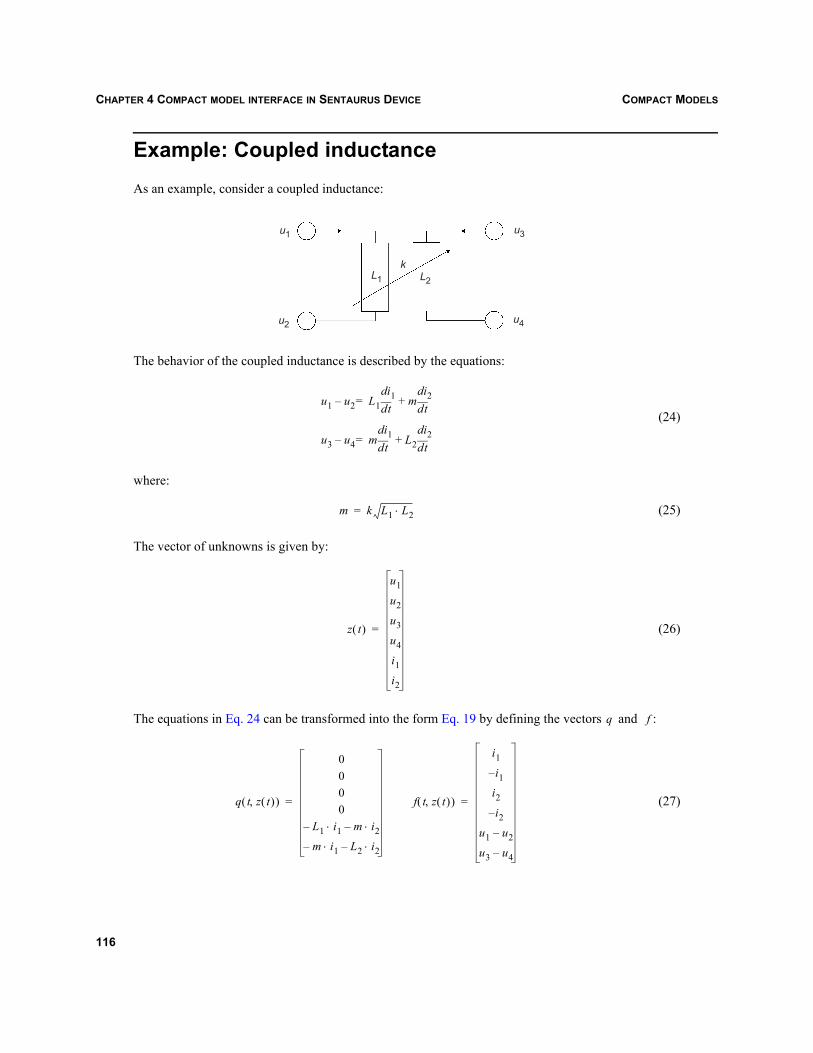
COMPACT MODELSCHAPTER 4 COMPACT MODEL INTERFACE IN SENTAURUS DEVICE
Example: Coupled inductanceAs an example, consider a coupled inductance:
The behavior of the coupled inductance is described by the equations:
(24)
where:
(25)
The vector of unknowns is given by:
(26)
The equations in Eq. 24 can be transformed into the form Eq. 19 by defining the vectors and :
(27)
u1
u2
u3
u4
kL1 L2
u1 u2– L= 1 tddi1 m td
di2+
u3 u4– m= tddi1 L2 td
di2+
m k L1 L2⋅=
z t( )
u1
u2
u3
u4
i1
i2
=
q f
q t z t( ),( )
0000
L1 i1⋅– m i2⋅–
m i1⋅– L2 i2⋅–
= f t z t( ),( )
i1
i– 1
i2
i2–
u1 u2–
u3 u4–
=
116

COMPACT MODELS CHAPTER 4 COMPACT MODEL INTERFACE IN SENTAURUS DEVICE
The Jacobians of and are given by:
(28)
State variables and parametersEach compact model can also have internal state variables, which can be used to hold auxiliaryinformation associated with the current operating point. However, Sentaurus Device does not providedirect support for state variables, and they must be updated by the models themselves during asimulation.
Furthermore, each compact model can have parameters (or attributes) to control its behavior. Usually,these parameters remain constant during a simulation but, occasionally, they can be modified, forexample, during a quasistationary command with a goal on a model parameter.
Plotting during transient simulationsSpecial attention is needed for plotting the electrode currents of compact models during transientsimulations. When Sentaurus Device plots the current flowing from an electrode into a compact model,it evaluates only the function to determine this current. In particular, the function isnot called. More precisely, Sentaurus Device only calls the function cmi_instance_get_rhs with toevaluate the DC right-hand side (see Interface subroutines on page 120).
Therefore, it is recommended that the model equations are set up so that the vector always containsthe currents flowing into the compact model. This requirement is easily satisfied by introducing internalvariables that represent the electrode currents. The coupled inductance previously discussed can be usedas an example.
NOTE This restriction only affects the value of the electrode currents used for plotting. SentaurusDevice always works with the correct current internally during a transient simulation.
q f
zdd q t z t( ),( ) Jq
0 0 0 0 0 00 0 0 0 0 00 0 0 0 0 00 0 0 0 0 00 0 0 0 L1– m–
0 0 0 0 m– L2–
= =
zdd f t z t( ),( ) Jf
0 0 0 0 1 00 0 0 0 1– 00 0 0 0 0 10 0 0 0 0 1–1 1– 0 0 0 00 0 1 1– 0 0
= =
f t z t( ),( ) q t z t( ),( )dc 0≠
f
117

COMPACT MODELSCHAPTER 4 COMPACT MODEL INTERFACE IN SENTAURUS DEVICE
Hierarchical description of compact modelsIn Sentaurus Device, each compact model is described by a three-level hierarchy:
Device The device describes the basic properties of a compact model. This includes thenames of the model, electrodes, thermodes, and internal variables, and thenames and types of the internal states and parameters.
Parameter set Each parameter set is derived from a device. It defines default values for theparameters of a compact model. Usually, the parameters that are shared amongseveral instances are defined in a parameter set.
Instance Instances correspond to the elements in a Sentaurus Device circuit. Eachinstance is derived from a parameter set. It can override the values of itsparameters if necessary.
For each user-defined compact model, the device, parameter set, and instance descriptions must appearin a compact circuit file with the extension .ccf. Instances can also appear in the Sentaurus Device Systemsection. For example, the model of a coupled inductance can be described by the compact circuit file:
DEVICE coupledELECTRODES
u1 // input voltage, highu2 // input voltage, lowu3 // output voltage, highu4 // output voltage, low
INTERNALSi1 // input currenti2 // output current
STATESdouble m // mutual inductance
PARAMETERSdouble ind1 // primary inductancedouble ind2 // secondary inductancedouble k // coupling factor
END DEVICE
PSET coupled_psetDEVICE coupledPARAMETERS
k = 1END PSET
INSTANCE coupled_instPSET coupled_psetELECTRODES n2 n0 n3 n0PARAMETERS
ind1 = 1e-3ind2 = 1e-3
END INSTANCE
Syntax of compact circuit files on page 128 presents the complete syntax of this language inBackus–Naur form.
118

COMPACT MODELS CHAPTER 4 COMPACT MODEL INTERFACE IN SENTAURUS DEVICE
Electrothermal modelsIn Sentaurus Device, circuit nodes are electrical by default. This means that their values are assumed tobe voltages. However nodes can also be declared to be thermal, in which case, their values correspondto temperatures [K]. Electrical nodes are part of the electrical circuit (Circuit), whereas thermal nodesbelong to the thermal circuit (TCircuit).
Sentaurus Device does not require that the electrodes of a compact model are connected to electricalcircuit nodes or that thermodes are connected to thermal circuit nodes. Such a restriction is undesirablebecause several devices can be used both in the electrical and thermal circuit. An example is a resistorthat can be used as an electrical resistor in Circuit and as a thermal resistor in TCircuit. Similarly, voltagesources can serve as heat sources or heat sinks in the thermal circuit.
The equations in Circuit and TCircuit can be solved independently or simultaneously, depending on thecommands in the Solve section:
coupled{Circuit}coupled{TCircuit}coupled{Circuit TCircuit}
This separation of equations is useful for certain types of simulation. It may be required to determine theDC operating point of a circuit by solving Circuit and TCircuit together. For a subsequent transientanalysis only, the Circuit equations must be solved. Of course, it is assumed that the temperatures do notchange during the transient simulation (which is a reasonable assumption for many problems).
For electrothermal models, Sentaurus Device imposes a restriction. The Circuit and TCircuit equationscan be solved simultaneously, but the Jacobian of the equations does not include the cross-terms orcouplings between the electrical and thermal equations. This restriction only affects models that areconnected to both electrical and thermal nodes. The results of the simulation will not change. However,the speed of convergence may be impaired.
If problems are encountered due to this restriction (slow convergence or nonconvergence), a simplesolution is to let all of the nodes in the System section be electrical, that is, do not declare any thermalnodes.
The temperature equations will then also become a part of Circuit, and the thermal equations will besolved simultaneously with the electrical equations.
NOTE This solution only applies to compact models. If a simulation involves physical devices withelectrodes and thermodes, connect the electrodes to electrical nodes and the thermodes tothermal nodes.
119

COMPACT MODELSCHAPTER 4 COMPACT MODEL INTERFACE IN SENTAURUS DEVICE
Data structures of Sentaurus DeviceThis section presents an overview on the C++ data structures that are used in the compact modelinterface. These C++ classes have been designed to give easy access to all necessary information whilehiding the implementation details in Sentaurus Device. The code in the corresponding header files is inHeader files on page 132.
The class CCMBaseParam is used to store the parameters of devices, parameter sets, and instances. Table 52lists the four basic types that are supported.
NOTE The memory of strings is managed by the class CCMBaseParam. In particular, the strings aredeallocated in the destructor ~CCMBaseParam by calling delete[].
The class CCMBaseParam can hold scalar or vector values of each basic type. The memory for the arrays isallocated and deallocated within the class itself. The method SetDimension resizes an array if necessary.
The classes CCMBaseDevice, CCMBasePSet, and CCMBaseInstance provide descriptors for devices, parametersets, and instances, respectively. The number of electrodes, thermodes, internal variables, states, andparameters is obtained from the model description in the compact circuit file. CCMBasePSet provides apointer to the device from which it was derived. Similarly, the class CCMBaseInstance has two pointers tothe parent parameter set and parent device.
The variables device_desc, pset_desc, and instance_desc are provided for use within the compact models.They represent a ‘hook’ to hold additional information within devices, parameter sets, and instances,which may be required by the compact models.
Interface subroutinesEach user-defined compact model must implement a set of well-defined interface subroutines. When theuser code is attached to Sentaurus Device, the dynamic linker searches for these subroutines in the objectfile.
NOTE All subroutines must conform to C linkage conventions. The prototypes of the interfacefunctions appear in the header file CMIModels.h.
Table 52 Basic data types
Data type C++ name Data type C++ name
Character char Real double
Integer int String char*
120

COMPACT MODELS CHAPTER 4 COMPACT MODEL INTERFACE IN SENTAURUS DEVICE
cmi_device_createvoid
cmi_device_create (CCMBaseDevice*const device);
This subroutine is called whenever a new device is created. It can be used to initialize the variabledevice_desc.
cmi_device_set_paramvoid
cmi_device_set_param (CCMBaseDevice*const device,const CCMBaseParam*const param);
This subroutine assigns a new value to a device parameter. It can be called several times beforecmi_device_initialize is invoked.
cmi_device_initializevoid
cmi_device_initialize (CCMBaseDevice*const device);
This subroutine is always invoked after the values of one or several parameters have been changed. Itcan be used to compute auxiliary variables that depend on the parameters.
cmi_device_get_paramvoid
cmi_device_get_param (CCMBaseDevice*const device, CCMBaseParam*const param);
This subroutine retrieves the value of a parameter. The parameter is identified by its name, that is, by thevalue of param->Name(). The result should be stored in *param.
cmi_device_deletevoid
cmi_device_delete (CCMBaseDevice*const device);
This subroutine is called whenever a device is deleted. It presents an opportunity to release the dynamicmemory associated with the device.
121

COMPACT MODELSCHAPTER 4 COMPACT MODEL INTERFACE IN SENTAURUS DEVICE
cmi_pset_createvoid
cmi_pset_create (CCMBasePSet*const pset);
This subroutine is called whenever a new parameter set is created. It can be used to initialize thevariable pset_desc.
cmi_pset_set_paramvoid
cmi_pset_set_param (CCMBasePSet*const pset,const CCMBaseParam*const param);
This subroutine assigns a new value to a parameter-set parameter. It can be called several times beforecmi_pset_initialize is invoked.
cmi_pset_initializevoid
cmi_pset_initialize (CCMBasePSet*const pset);
This subroutine is always invoked after the values of one or several parameters have been changed. Itcan be used to compute auxiliary variables that depend on the parameters.
cmi_pset_get_paramvoid
cmi_pset_get_param (CCMBasePSet*const pset,CCMBaseParam*const param);
This subroutine retrieves the value of a parameter. The parameter is identified by its name, that is, by thevalue of param->Name(). The result should be stored in *param.
cmi_pset_deletevoid
cmi_pset_delete (CCMBasePSet*const pset);
This subroutine is called whenever a parameter set is deleted. It presents an opportunity to release thedynamic memory associated with the parameter set.
122

COMPACT MODELS CHAPTER 4 COMPACT MODEL INTERFACE IN SENTAURUS DEVICE
cmi_instance_createvoid
cmi_instance_create (CCMBaseInstance*const instance);
This subroutine is called whenever a new instance is created. It can be used to initialize thevariable instance_desc.
cmi_instance_set_paramvoid
cmi_instance_set_param (CCMBaseInstance*const instance,const CCMBaseParam*const param);
This subroutine assigns a new value to an instance parameter. It can be called several times beforecmi_instance_initialize is invoked.
cmi_instance_initializevoid
cmi_instance_initialize (CCMBaseInstance*const instance);
This subroutine is always invoked after the values of one or several parameters have changed. It can beused to compute auxiliary variables that depend on the parameters.
cmi_instance_get_paramvoid
cmi_instance_get_param (CCMBaseInstance*const instance,CCMBaseParam*const param);
This subroutine retrieves the value of a parameter. The parameter is identified by its name, that is, by thevalue of param->Name(). The result should be stored in *param.
cmi_instance_get_rhsvoid
cmi_instance_get_rhs (CCMBaseInstance*const instance,const int dc, const double time,const double*const variables,double*const rhs);
This subroutine computes either the DC right-hand side (if ) or the transient right-hand side (if ).
f dc 0≠ qdc 0=
123

COMPACT MODELSCHAPTER 4 COMPACT MODEL INTERFACE IN SENTAURUS DEVICE
The simulation time is passed in the parameter time. The array variables contains the values of thesystem variables, that is, electrode voltages, thermode temperatures, and internal variables. The lengthof variables is given by instance->NumberVariables(). The result must be stored in rhs, which is also anarray of size instance->NumberVariables().
cmi_instance_get_jacobianvoid
cmi_instance_get_jacobian (CCMBaseInstance*const instance,const int dc, const double time,const double*const variables,double*const*const jacobian);
This subroutine computes either the DC Jacobian (if ) or the transient Jacobian (if ).
The simulation time is passed in the parameter time. The array variables contains the values of thesystem variables, that is, electrode voltages, thermode temperatures, and internal variables. The lengthof variables is given by instance->NumberVariables(). The result must be stored in jacobian, which is asquare matrix of dimension instance->NumberVariables().
cmi_instance_is_physicalint
cmi_instance_is_physical (CCMBaseInstance*const instance,const double time,const double*const variables);
This subroutine determines if the given operating point lies within the valid model range. The parametertime represents the simulation time, and the system variables are passed in the parameter variables, anarray of size instance->NumberVariables().
This subroutine is called whenever a simulation step has converged. If the computed solution isacceptable, cmi_instance_is_physical returns 1. Otherwise, the value 0 is returned.
A model can also control the time step during a transient simulation by calling the subroutines describedin Run-time support.
cmi_instance_deletevoid
cmi_instance_delete (CCMBaseInstance*const instance);
This subroutine is called whenever an instance is deleted. It presents an opportunity to release thedynamic memory associated with the instance.
Jf dc 0≠ Jq dc 0=
124

COMPACT MODELS CHAPTER 4 COMPACT MODEL INTERFACE IN SENTAURUS DEVICE
Run-time supportSentaurus Device provides several subroutines to support the operation of compact models. Thesubroutines can be used to control the progress of an ongoing simulation.
cmi_starttimedouble
cmi_starttime ();
This function returns the start time of a transient simulation.
cmi_stoptimedouble
cmi_stoptime ();
This function returns the stop time of a transient simulation.
cmi_min_timestepdouble
cmi_min_timestep ();
This function returns the minimum step size of Sentaurus Device during a transient simulation.
cmi_max_timestepdouble
cmi_max_timestep ();
This function returns the maximum step size of Sentaurus Device during a transient simulation.
cmi_set_eventvoid
cmi_set_event (const double time);
This subroutine informs Sentaurus Device to synchronize with a given point in time during a transientsimulation.
125

COMPACT MODELSCHAPTER 4 COMPACT MODEL INTERFACE IN SENTAURUS DEVICE
cmi_set_max_timestepvoid
cmi_set_max_timestep (const double stepsize);
This subroutine limits the step size of Sentaurus Device during a transient simulation.
CompilationSentaurus Device tries to load the code of a compact model from an external shared-object file. The filename of the shared object file must be identical to the name of the device, and the file extension mustbe .so.arch. The extension arch depends on the architecture listed in Table 53.
Special compiler flags must be used to produce a shared-object file with position-independent code. Thescript cmi manages all the architecture-dependent details and is invoked by:
cmi options files
Table 54 lists the available options.
Table 53 Shared object file extensions
Architecture Extension Architecture Extension
AMD 64-bit amd64 Sun Solaris 8 solaris8
HP-UX 11 hppa11_64 Windows XP winxp
Red Hat Enterprise Linux linux_gnu
Table 54 Options of cmi
Option Purpose
-c Suppresses linking and produce an .o file for each source file.
-Dname=def Defines a macro symbol to the preprocessor. The assignment =def is optional.
-g Prepares the object files for debugging.
-h Shows a help message.
-Ipathname Appends pathname to the list of directories that are searched to look for #include files.
-llib Specifies an additional library for linking with object files.
-Lpathname Appends pathname to the list of directories that are searched by the linker.
-O Produces optimized code.
126
COMPACT MODELS CHAPTER 4 COMPACT MODEL INTERFACE IN SENTAURUS DEVICE
Files ending in .C, .cc, or .cxx are assumed to be C++ source files. Files with the extension .o are directlypassed to the linker.
Command file of Sentaurus DeviceTo load external compact models into Sentaurus Device, the search path CMIPath must be defined in theFile section of the command file of Sentaurus Device. The value of CMIPath consists of a sequence ofdirectories, for example:
File {CMIPath = ". /home/paper/lib /home/pencil/sdevice/lib"
}
The given directories are searched for compact circuit files (extension .ccf) and the correspondingshared-object files (extension .so.arch). Instances of compact models can also appear in the Systemsection of the command file. In this case, use the correct syntax, for example:
System {Electrical (n0 n1 n2 n3)coupled_pset coupled_inst (n2 n0 n3 n0) {ind1 = 1e-3 ind2 = 1e-3}
}
SummaryTo add external compact models to Sentaurus Device:
1. Collect the equations as in Eq. 17 for the compact model. Define the electrodes, thermodes, andinternal variables that are needed. For each electrode, compute the current flowing into the device.For each thermode, compute the heat flow into the device. For each internal variable, provide acorresponding model equation. Define the model parameters and their types.
2. Write a compact circuit file with the extension .ccf. Assign default values to the parameters (this isusually performed on the level of a device or parameter set).
3. Implement all the interface subroutines of Interface subroutines on page 120.
4. Use the script cmi to compile the model code and produce a shared-object file with the extension.so.arch. Each shared-object file must correspond exactly to one compact model, and the file namemust be identical to the device name of the compact model.
5. Define the variable CMIPath in the File section of the command file of Sentaurus Device. This definesthe search path for all the .ccf and .so.arch files.
-Uname Removes any initial definition of a macro symbol.
-v Displays the compiler command.
Table 54 Options of cmi
Option Purpose
127

COMPACT MODELSCHAPTER 4 COMPACT MODEL INTERFACE IN SENTAURUS DEVICE
6. The instances of the compact model are usually defined in the .ccf files. However, they can alsoappear in the System section of the command file of Sentaurus Device. In this case, use the correctsyntax of the command file of Sentaurus Device.
7. Run Sentaurus Device to perform the simulation.
Syntax of compact circuit filesThe grammar of a compact circuit file can be defined in Backus–Naur form (BNF). The symbol denotes empty production. Terminal symbols are in Courier font. Identifiers are sequences of letters anddigits. The first character must be a letter. An underscore (_) is also considered to be a letter.
CCMStrFile ε
| Descriptors
Descriptors Device
| PSet
| Instance
| Device Descriptors
| PSet Descriptors
| Instance Descriptors
Device DeviceHeader DeviceElectrodes DeviceThermodes DeviceInternals DeviceStates DeviceParams DeviceFooter
DeviceHeader DEVICE DeviceName
DeviceName Identifier
DeviceElectrodes ε
| ELECTRODES
| ELECTRODES DeviceElectrodeList
DeviceElectrodeList DeviceElectrode
| DeviceElectrode DeviceElectrodeList
DeviceElectrode Identifier
DeviceThermodes ε
| THERMODES
| THERMODES DeviceThermodeList
DeviceThermodeList DeviceThermode
| DeviceThermode DeviceThermodeList
DeviceThermode Identifier
DeviceInternals ε
ε
128

COMPACT MODELS CHAPTER 4 COMPACT MODEL INTERFACE IN SENTAURUS DEVICE
| INTERNALS
| INTERNALS DeviceInternalList
DeviceInternalList DeviceInternal
| DeviceInternal DeviceInternalList
DeviceInternal Identifier
DeviceStates ε
| STATES
| STATES DeviceStateList
DeviceStateList DeviceState
| DeviceState DeviceStateList
DeviceState SimpleType StateName
| SimpleType StateName [ Dimension ]
StateName Identifier
DeviceParams ε
| PARAMETERS
| PARAMETERS DeviceParamList
DeviceParamList DeviceParam
| DeviceParam DeviceParamList
DeviceParam SimpleType ParamName
| SimpleType ParamName ParamDefault
| SimpleType ParamName [ Dimension ]
| SimpleType ParamName [ Dimension ] ParamDefault
SimpleType char
| int
| double
| string
Dimension ε
| Integer
ParamDefault = ParamValue
DeviceFooter END DEVICE
PSet PSetHeader PSetDevice PSetParams PSetFooter
PSetHeader PSET PSetName
PSetName Identifier
129
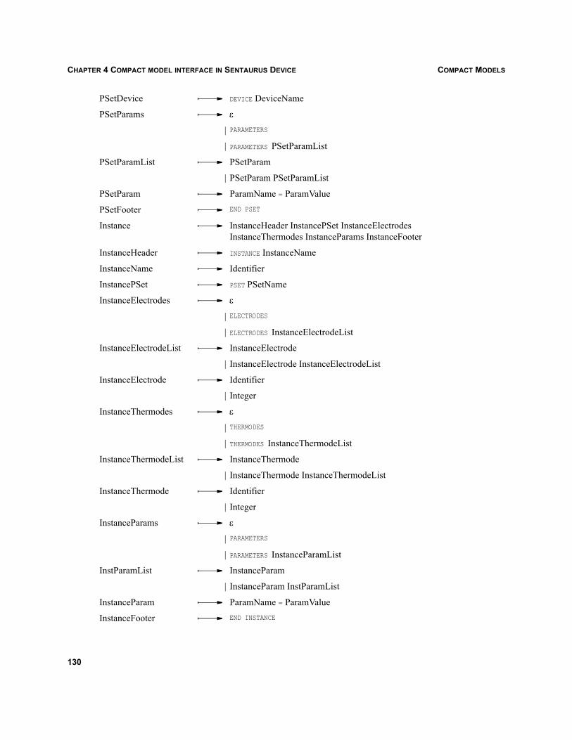
COMPACT MODELSCHAPTER 4 COMPACT MODEL INTERFACE IN SENTAURUS DEVICE
PSetDevice DEVICE DeviceName
PSetParams ε
| PARAMETERS
| PARAMETERS PSetParamList
PSetParamList PSetParam
| PSetParam PSetParamList
PSetParam ParamName = ParamValue
PSetFooter END PSET
Instance InstanceHeader InstancePSet InstanceElectrodes InstanceThermodes InstanceParams InstanceFooter
InstanceHeader INSTANCE InstanceName
InstanceName Identifier
InstancePSet PSET PSetName
InstanceElectrodes ε
| ELECTRODES
| ELECTRODES InstanceElectrodeList
InstanceElectrodeList InstanceElectrode
| InstanceElectrode InstanceElectrodeList
InstanceElectrode Identifier
| Integer
InstanceThermodes ε
| THERMODES
| THERMODES InstanceThermodeList
InstanceThermodeList InstanceThermode
| InstanceThermode InstanceThermodeList
InstanceThermode Identifier
| Integer
InstanceParams ε
| PARAMETERS
| PARAMETERS InstanceParamList
InstParamList InstanceParam
| InstanceParam InstParamList
InstanceParam ParamName = ParamValue
InstanceFooter END INSTANCE
130

COMPACT MODELS CHAPTER 4 COMPACT MODEL INTERFACE IN SENTAURUS DEVICE
In ScalarValue, Table 55 lists the values that are recognized.
Real values can also consist of fixed point numbers with a scaling factor as listed in Table 56.
ParamName Identifier
ParamValue VectorValue
| ScalarValue
VectorValue [ ]
| [ ScalarList ]
ScalarList ScalarValue
| ScalarValue ScalarList
ScalarValue Character
| Integer
| Real
| String
Table 55 Scalar values
Type Value Example
Character A character enclosed in single quotation marks. 'c'
Integer An optionally signed sequence of digits. 1, +2, -33
Real An integer, a fixed point value, or a floating point value as in C++. 1, -2.0, 3.4e-5
String A string consisting of a sequence of characters enclosed in double quotation marks.
"hello world"
Table 56 Scaling factors
Scaling factor Value Example Scaling factor Value Example
t (tera) 1.2t = u (micro) 7u =
g (giga) -2.3g = n (nano) 8n =
meg (mega) 4meg = p (pico) 5.6p =
k (kilo) 5k = f (femto) 0.2f =
m (milli) -3.2m = a (atto) 2a =
1012 1.2 1012× 10 6– 7 10 6–×
109 2.3– 109× 10 9– 8 10 9–×
106 4 106× 10 12– 5.6 10 12–×
103 5 103× 10 15– 0.2 10 15–×
10 3– 3.2– 10 3–× 10 18– 2 10 18–×
131

COMPACT MODELSCHAPTER 4 COMPACT MODEL INTERFACE IN SENTAURUS DEVICE
Header filesThe following header files are available for the implementation of compact models. These files are alsoin the directory $STROOT/tcad/$STRELEASE/lib/sdevice/include.
CCMBaseParam.henum CCMType {CCMType_c_char,CCMType_c_int,CCMType_c_double,CCMType_c_string
};
union CCMData {// scalarschar c;int i;double d;char* s;// vectorschar* c_vec;int* i_vec;double* d_vec;char** s_vec;
};
// helper class for CCMBaseParamclass CCMBaseParam_Index_Holder_read {friend class CCMBaseParam_Index_Holder_read_write;friend class CCMBaseParam;
const CCMBaseParam& w_param;int w_index;
CCMBaseParam_Index_Holder_read (const CCMBaseParam& parameter, int index);
public:
// readoperator char () const;operator int () const;operator double () const;operator const char* () const;
};
// helper class for CCMBaseParamclass CCMBaseParam_Index_Holder_read_write {friend class CCMBaseParam_Index_Holder_read;friend class CCMBaseParam;
CCMBaseParam& w_param;int w_index;
132

COMPACT MODELS CHAPTER 4 COMPACT MODEL INTERFACE IN SENTAURUS DEVICE
CCMBaseParam_Index_Holder_read_write (CCMBaseParam& parameter, int index);
public:
// readoperator char () const;operator int () const;operator double () const;operator const char* () const;
// writevoid operator = (const char value);void operator = (const int value);void operator = (const double value);void operator = (const char* value);void operator = (const CCMBaseParam& value);void operator = (const CCMBaseParam_Index_Holder_read value);void operator = (const CCMBaseParam_Index_Holder_read_write value);
};
class CCMBaseParam {friend class CCMBaseParam_Index_Holder_read;friend class CCMBaseParam_Index_Holder_read_write;friend class CCMParam;
void Allocate ();// allocate arrays if this is a vector
void Deallocate ();// deallocate arrays if this is a vector
char* name; // name of the parameter (is used as key)const CCMType type; // type of the parameterconst int isvector; // is this a vector?int dimension; // dimension of vector, if isvectorint defined; // is the value of this parameter defined?CCMData w_value; // value of parameter, if defined
public:
CCMBaseParam (const char*const paramname, const CCMType paramtype,const int paramisvector, const int paramdimension);
CCMBaseParam (const CCMBaseParam& param);
virtual ~CCMBaseParam ();
const char* Name () const{ return name; }
CCMType Type () const{ return type; }
int IsVector () const{ return isvector; }
int Dimension () const
133

COMPACT MODELSCHAPTER 4 COMPACT MODEL INTERFACE IN SENTAURUS DEVICE
{ return dimension; }
void SetDimension (const int dim);// resize the vector// the old values are lost
int Defined () const{ return defined; }
void Defined (const int def){ defined = def; }
// conversion operatorsoperator char () const;operator int () const;operator double () const;operator const char* () const;
// assignment operatorsvoid operator = (const char value);void operator = (const int value);void operator = (const double value);void operator = (const char* value);void operator = (const CCMBaseParam& value);void operator = (const CCMBaseParam_Index_Holder_read value);void operator = (const CCMBaseParam_Index_Holder_read_write value);
// array accessconst CCMBaseParam_Index_Holder_read operator [] (const int index) const;CCMBaseParam_Index_Holder_read_write operator [] (const int index);
virtual void Print (std::ostream& stream) const;// print the parameter
};
std::ostream& operator << (std::ostream& stream, const CCMBaseParam* par);
CCMBaseDevice.hclass CCMBaseDevice {
protected:
char* devicename; // name of this device
const int w_num_electrodes; // number of electrodes const int w_num_thermodes; // number of thermodes const int w_num_internals; // number of internal variables const int w_num_variables; // total number of variables
// w_num_variables == w_num_electrodes + // w_num_thermodes + // w_num_internals
const int w_num_states; // number of internal statesconst int w_num_parameters; // number of parameters
public:
134

COMPACT MODELS CHAPTER 4 COMPACT MODEL INTERFACE IN SENTAURUS DEVICE
void* device_desc; // user device descriptor
CCMBaseDevice (const char*const name, const int num_electrodes, const int num_thermodes, const int num_internals,
const int num_states, const int num_parameters);
virtual ~CCMBaseDevice ();
const char* Name () const { return devicename; }; // return the name of the device
int NumberElectrodes () const { return w_num_electrodes; }; // return the number of electrodes
int NumberThermodes () const { return w_num_thermodes; }; // return the number of thermodes
int NumberInternals () const { return w_num_internals; }; // return the number of internal variables
int NumberVariables () const { return w_num_variables; };// return the total number of variables
int NumberStates () const { return w_num_states; }; // return the number of internal states
int NumberParameters () const { return w_num_parameters; } // return the number of parameters};
CCMBasePSet.hclass CCMBasePSet {
protected:
char* psetname; // name of this parameter set
const int w_num_electrodes; // number of electrodes const int w_num_thermodes; // number of thermodes const int w_num_internals; // number of internal variables const int w_num_variables; // total number of variables // w_num_variables == w_num_electrodes + // w_num_thermodes + // w_num_internals const int w_num_states; // number of internal states const int w_num_parameters; // number of parameters
CCMBaseDevice* CCMBasedevice; // backpointer to CCMBase device
public:
void* pset_desc; // user parameter set descriptor
CCMBasePSet (const char*const name, CCMBaseDevice*const device);
135

COMPACT MODELSCHAPTER 4 COMPACT MODEL INTERFACE IN SENTAURUS DEVICE
virtual ~CCMBasePSet ();
const char* Name () const { return psetname; };// return the name of the parameter set
int NumberElectrodes () const { return w_num_electrodes; };// return the number of electrodes
int NumberThermodes () const { return w_num_thermodes; };// return the number of thermodes
int NumberInternals () const { return w_num_internals; };// return the number of internal variables
int NumberVariables () const { return w_num_variables; };// return the total number of variables
int NumberStates () const { return w_num_states; };// return the number of internal states
int NumberParameters () const { return w_num_parameters; }// return the number of parameters
CCMBaseDevice* GetCCMBaseDevice () const { return CCMBasedevice; };// return the parent device
};
CCMBaseInstance.hclass CCMBaseInstance {
protected:
char* instancename; // name of this instance
const int w_num_electrodes; // number of electrodes const int w_num_thermodes; // number of thermodes int w_num_internals; // number of internal variables int w_num_variables; // total number of variables // w_num_variables == w_num_electrodes +
// w_num_thermodes +// w_num_internals
const int w_num_states; // number of internal states const int w_num_parameters; // number of parameters
CCMBasePSet* CCMBasepset; // backpointer to CCMBase parameter set CCMBaseDevice* CCMBasedevice; // backpointer to CCMBase device
public:
void* instance_desc; // user instance descriptor
CCMBaseInstance (const char*const name, CCMBasePSet*const pset);
virtual ~CCMBaseInstance ();
136
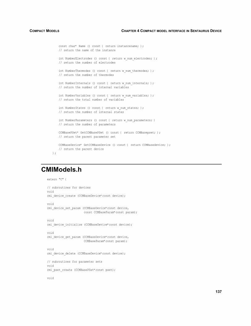
COMPACT MODELS CHAPTER 4 COMPACT MODEL INTERFACE IN SENTAURUS DEVICE
const char* Name () const { return instancename; }; // return the name of the instance
int NumberElectrodes () const { return w_num_electrodes; }; // return the number of electrodes
int NumberThermodes () const { return w_num_thermodes; }; // return the number of thermodes
int NumberInternals () const { return w_num_internals; }; // return the number of internal variables
int NumberVariables () const { return w_num_variables; }; // return the total number of variables
int NumberStates () const { return w_num_states; }; // return the number of internal states
int NumberParameters () const { return w_num_parameters; } // return the number of parameters
CCMBasePSet* GetCCMBasePSet () const { return CCMBasepset; }; // return the parent parameter set
CCMBaseDevice* GetCCMBaseDevice () const { return CCMBasedevice; }; // return the parent device
};
CMIModels.hextern "C" {
// subroutines for devicesvoidcmi_device_create (CCMBaseDevice*const device);
voidcmi_device_set_param (CCMBaseDevice*const device, const CCMBaseParam*const param);
voidcmi_device_initialize (CCMBaseDevice*const device);
voidcmi_device_get_param (CCMBaseDevice*const device, CCMBaseParam*const param);
voidcmi_device_delete (CCMBaseDevice*const device);
// subroutines for parameter setsvoidcmi_pset_create (CCMBasePSet*const pset);
void
137

COMPACT MODELSCHAPTER 4 COMPACT MODEL INTERFACE IN SENTAURUS DEVICE
cmi_pset_set_param (CCMBasePSet*const pset, const CCMBaseParam*const param);
voidcmi_pset_initialize (CCMBasePSet*const pset);
voidcmi_pset_get_param (CCMBasePSet*const pset, CCMBaseParam*const param);
voidcmi_pset_delete (CCMBasePSet*const pset);
// subroutines for instancesvoidcmi_instance_create (CCMBaseInstance*const instance);
voidcmi_instance_set_param (CCMBaseInstance*const instance, const CCMBaseParam*const param);
voidcmi_instance_initialize (CCMBaseInstance*const instance);
voidcmi_instance_get_param (CCMBaseInstance*const instance, CCMBaseParam*const param);
voidcmi_instance_get_rhs (CCMBaseInstance*const instance, const int dc, const double time, const double*const variables, double*const rhs);
voidcmi_instance_get_jacobian (CCMBaseInstance*const instance, const int dc, const double time, const double*const variables, double*const*const jacobian);
intcmi_instance_is_physical (CCMBaseInstance*const instance, const double time, const double*const variables);
voidcmi_instance_delete (CCMBaseInstance*const instance);
} // extern "C"
138

COMPACT MODELS CHAPTER 4 COMPACT MODEL INTERFACE IN SENTAURUS DEVICE
CMISupport.hdoublecmi_starttime ();// Returns the starttime of a transient simulation.
doublecmi_stoptime ();// Returns the stoptime of a transient simulation.
doublecmi_min_timestep ();// Returns the minimum stepsize of Sentaurus Device// during a transient simulation.
doublecmi_max_timestep ();// Returns the maximum stepsize of Sentaurus Device// during a transient simulation.
voidcmi_set_event (const double time);// This subroutine tells Sentaurus Device to synchronize with// a given point in time during a transient simulation.
voidcmi_set_max_timestep (const double stepsize);// This subroutine limits the stepsize of Sentaurus Device// during a transient simulation.
Coupled inductancesThis section shows the implementation of coupled inductances as a compact model. The correspondingequations are in Model equations on page 113.
NOTE Coupled inductances are also available as a SPICE model (see Inductor on page 5 andCoupled (mutual) inductors on page 5).
The source files for this example are in the directory $STROOT/tcad/$STRELEASE/lib/sdevice/src/dynamic.
coupled.ccfDEVICE coupled
ELECTRODESu1 // input voltage, highu2 // input voltage, lowu3 // output voltage, highu4 // output voltage, low
139

COMPACT MODELSCHAPTER 4 COMPACT MODEL INTERFACE IN SENTAURUS DEVICE
INTERNALSi1 // input currenti2 // output current
STATESdouble m // mutual inductance
PARAMETERSdouble ind1 // primary inductancedouble ind2 // secondary inductancedouble k // coupling factor
END DEVICE
PSET coupled_psetDEVICE coupledPARAMETERS
k = 1END PSET
coupled.C#include <stdlib.h>#include <string.h>#include <iostream.h>#include <math.h>
#include "CMIModels.h"#include "CMISupport.h"
class Parameters {public:
double ind1;double ind2;double k;
Parameters ();void Set (const CCMBaseParam* param);void Get (CCMBaseParam* param);
};
Parameters::Parameters () :
ind1 (0.0),ind2 (0.0),k (1.0)
{}
void Parameters::Set (const CCMBaseParam* param){ if (param->Defined ()) { if (strcmp (param->Name (), "ind1") == 0) { ind1 = *param; } else if (strcmp (param->Name (), "ind2") == 0) { ind2 = *param; } else if (strcmp (param->Name (), "k") == 0) { k = *param; }
140

COMPACT MODELS CHAPTER 4 COMPACT MODEL INTERFACE IN SENTAURUS DEVICE
}}
void Parameters::Get (CCMBaseParam* param){ if (strcmp (param->Name (), "ind1") == 0) { *param = ind1; param->Defined (1);} else if (strcmp (param->Name (), "ind2") == 0) {
*param = ind2; param->Defined (1);} else if (strcmp (param->Name (), "k") == 0) {
*param = k; param->Defined (1);} else {
param->Defined (0);}
}
class Device {public:
Parameters par;};
class PSet {public:
Parameters par;};
class Instance {public:
Parameters par;double m;
};
extern "C" voidcmi_device_create (CCMBaseDevice*const device){ device->device_desc = new Device;}
extern "C" voidcmi_device_set_param (CCMBaseDevice*const device, const CCMBaseParam*const param){ Device* dev = (Device*) device->device_desc;dev->par.Set (param);
}
extern "C" voidcmi_device_initialize (CCMBaseDevice*const device){}
extern "C" voidcmi_device_get_param (CCMBaseDevice*const device, CCMBaseParam*const param){ Device* dev = (Device*) device->device_desc;dev->par.Get (param);
}
141

COMPACT MODELSCHAPTER 4 COMPACT MODEL INTERFACE IN SENTAURUS DEVICE
extern "C" voidcmi_device_delete (CCMBaseDevice*const device){ delete (Device*) device->device_desc;}
extern "C" voidcmi_pset_create (CCMBasePSet*const pset){ pset->pset_desc = new PSet;}
extern "C" voidcmi_pset_set_param (CCMBasePSet*const pset, const CCMBaseParam*const param){ PSet* ps = (PSet*) pset->pset_desc;ps->par.Set (param);
}
extern "C" voidcmi_pset_initialize (CCMBasePSet*const pset){}
extern "C" voidcmi_pset_get_param (CCMBasePSet*const pset, CCMBaseParam*const param){ PSet* ps = (PSet*) pset->pset_desc;ps->par.Get (param);
}
extern "C" voidcmi_pset_delete (CCMBasePSet*const pset){ delete (PSet*) pset->pset_desc;}
extern "C" voidcmi_instance_create (CCMBaseInstance*const instance){ instance->instance_desc = new Instance;}
extern "C" voidcmi_instance_set_param (CCMBaseInstance*const instance, const CCMBaseParam*const param){ Instance* inst = (Instance*) instance->instance_desc;inst->par.Set (param);
}
extern "C" voidcmi_instance_initialize (CCMBaseInstance*const instance){ Instance* inst = (Instance*) instance->instance_desc;inst->m = inst->par.k * sqrt (inst->par.ind1 * inst->par.ind2);
}
extern "C" voidcmi_instance_get_param (CCMBaseInstance*const instance, CCMBaseParam*const param){ Instance* inst = (Instance*) instance->instance_desc;inst->par.Get (param);
142

COMPACT MODELS CHAPTER 4 COMPACT MODEL INTERFACE IN SENTAURUS DEVICE
}
#define u1 (variables [0])#define u2 (variables [1])#define u3 (variables [2])#define u4 (variables [3])#define i1 (variables [4])#define i2 (variables [5])
extern "C" voidcmi_instance_get_rhs (CCMBaseInstance*const instance, const int dc, const double time, const double*const variables, double*const rhs){ Instance* inst = (Instance*) instance->instance_desc;if (dc) {
rhs [0] = i1; rhs [1] = -i1; rhs [2] = i2; rhs [3] = -i2; rhs [4] = u1-u2; rhs [5] = u3-u4;} else {
rhs [4] = -inst->par.ind1 * i1 - inst->m * i2; rhs [5] = -inst->par.ind2 * i2 - inst->m * i1;}
}
extern "C" voidcmi_instance_get_jacobian (CCMBaseInstance*const instance, const int dc, const double time, const double*const variables, double*const*const jacobian){ Instance* inst = (Instance*) instance->instance_desc;if (dc) {
jacobian[0][4] = 1.0; jacobian[1][4] = -1.0; jacobian[2][5] = 1.0; jacobian[3][5] = -1.0; jacobian[4][0] = 1.0; jacobian[4][1] = -1.0; jacobian[5][2] = 1.0; jacobian[5][3] = -1.0;} else {
jacobian[4][4] = -inst->par.ind1; jacobian[4][5] = -inst->m; jacobian[5][4] = -inst->m; jacobian[5][5] = -inst->par.ind2;}
}
extern "C" intcmi_instance_is_physical (CCMBaseInstance*const instance, const double time, const double*const variables){ return 1;}
143

COMPACT MODELSCHAPTER 4 COMPACT MODEL INTERFACE IN SENTAURUS DEVICE
extern "C" voidcmi_instance_delete (CCMBaseInstance*const instance){ delete (Instance*) instance->instance_desc;}
Electrothermal resistanceIn this section, the equations for an electrothermal resistance are presented.
NOTE This model is also available as the built-in model Ter (see Electrothermal resistor onpage 110).
An electrothermal resistance has three contacts (two electrodes and one thermode):
The electrical behavior of the resistance is described by Ohm’s law:
(29)
The resistance of the device, however, depends on the thermode temperature:
(30)
On the other hand, the device also produces Joule heat, which is dissipated through the thermode:
(31)
The device can be described by the following vector of unknowns:
(32)
u1i
t1
u2R
u1 u2– R i⋅=
R r 1 α t1 tref–( ) β t1 tref–( )2⋅+⋅+( )⋅=
P u1 u2–( ) i⋅=
z t( )
u1
u2
t1
i
=
144

COMPACT MODELS CHAPTER 4 COMPACT MODEL INTERFACE IN SENTAURUS DEVICE
The DC right-hand side is given by:
(33)
The first two entries of correspond to the current flowing into the device through the electrodesand . The third entry of represents the heat flow into the device through the thermode .
Eq. 29 and Eq. 31 have no derivatives with regard to time. Therefore, the transient right-hand side iszero. The Jacobian of is given by:
(34)
where:
(35)
tres.ccfDEVICE tres
ELECTRODESu1 // input voltage 1u2 // input voltage 2
THERMODESt1 // thermode for Joule heat
INTERNALSi // current through resistor
PARAMETERSdouble r = 1 // resistancedouble alpha = 0 // linear temperature coefficientdouble beta = 0 // quadratic temperature coefficientdouble tref = 300.15 // reference temperature
END DEVICE
PSET tres_psetDEVICE tres
END PSET
fR t z t( ),( )
ii–
u1 u2–( )– i⋅
u1 u2– R i⋅–
=
fR u1u2 fR t1
fR
zdd fR t z t( ),( ) JfR
0 0 0 10 0 0 1–i– i 0 u1 u2–( )–
1 1– t1ddR– i⋅ R–
= =
t1ddR r α 2 β t1 tref–( )⋅ ⋅+( )⋅=
145
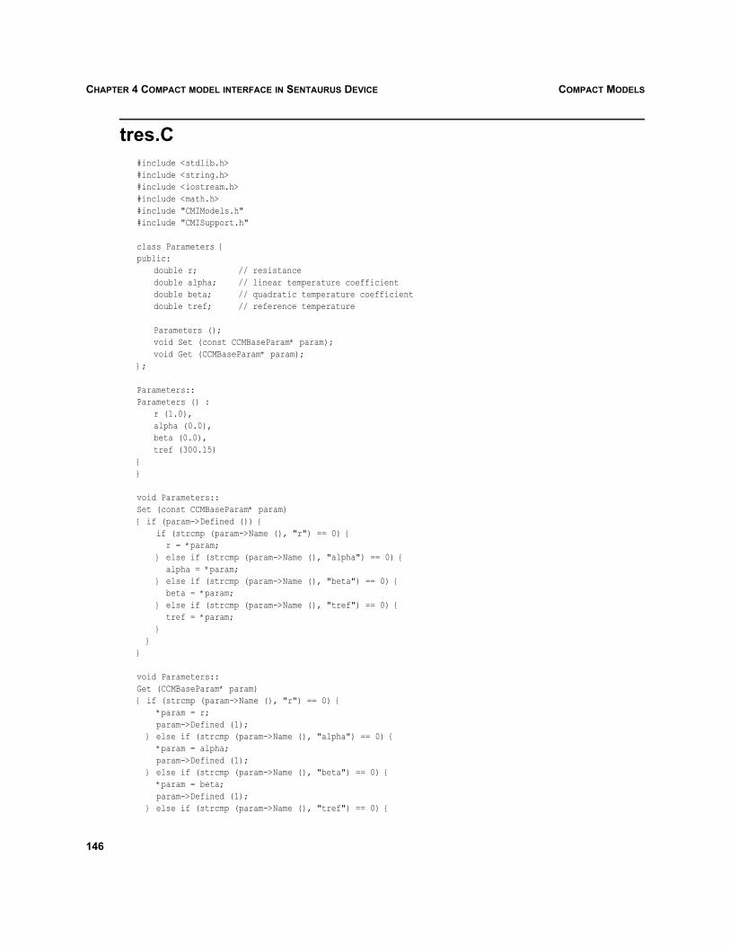
COMPACT MODELSCHAPTER 4 COMPACT MODEL INTERFACE IN SENTAURUS DEVICE
tres.C#include <stdlib.h>#include <string.h>#include <iostream.h>#include <math.h>#include "CMIModels.h"#include "CMISupport.h"
class Parameters {public:
double r; // resistancedouble alpha; // linear temperature coefficientdouble beta; // quadratic temperature coefficientdouble tref; // reference temperature
Parameters ();void Set (const CCMBaseParam* param);void Get (CCMBaseParam* param);
};
Parameters::Parameters () :
r (1.0),alpha (0.0),beta (0.0),tref (300.15)
{}
void Parameters::Set (const CCMBaseParam* param){ if (param->Defined ()) { if (strcmp (param->Name (), "r") == 0) { r = *param; } else if (strcmp (param->Name (), "alpha") == 0) { alpha = *param; } else if (strcmp (param->Name (), "beta") == 0) { beta = *param; } else if (strcmp (param->Name (), "tref") == 0) { tref = *param; }}
}
void Parameters::Get (CCMBaseParam* param){ if (strcmp (param->Name (), "r") == 0) { *param = r; param->Defined (1);} else if (strcmp (param->Name (), "alpha") == 0) {
*param = alpha; param->Defined (1);} else if (strcmp (param->Name (), "beta") == 0) {
*param = beta; param->Defined (1);} else if (strcmp (param->Name (), "tref") == 0) {
146

COMPACT MODELS CHAPTER 4 COMPACT MODEL INTERFACE IN SENTAURUS DEVICE
*param = tref; param->Defined (1);} else {
param->Defined (0);}
}class Device {public:
Parameters par;};class PSet {public:
Parameters par;};
class Instance {public:
Parameters par;};
extern "C" voidcmi_device_create (CCMBaseDevice*const device){ device->device_desc = new Device;}
extern "C" voidcmi_device_set_param (CCMBaseDevice*const device, const CCMBaseParam*const param){ Device* dev = (Device*) device->device_desc;dev->par.Set (param);
}
extern "C" voidcmi_device_initialize (CCMBaseDevice*const device){}
extern "C" voidcmi_device_get_param (CCMBaseDevice*const device, CCMBaseParam*const param){ Device* dev = (Device*) device->device_desc;dev->par.Get (param);
}
extern "C" voidcmi_device_delete (CCMBaseDevice*const device){ delete (Device*) device->device_desc;}
extern "C" voidcmi_pset_create (CCMBasePSet*const pset){ pset->pset_desc = new PSet;}
extern "C" voidcmi_pset_set_param (CCMBasePSet*const pset, const CCMBaseParam*const param){ PSet* ps = (PSet*) pset->pset_desc;
147

COMPACT MODELSCHAPTER 4 COMPACT MODEL INTERFACE IN SENTAURUS DEVICE
ps->par.Set (param);}
extern "C" voidcmi_pset_initialize (CCMBasePSet*const pset){}
extern "C" voidcmi_pset_get_param (CCMBasePSet*const pset, CCMBaseParam*const param)
{ PSet* ps = (PSet*) pset->pset_desc;ps->par.Get (param);
}
extern "C" voidcmi_pset_delete (CCMBasePSet*const pset){ delete (PSet*) pset->pset_desc;}
extern "C" voidcmi_instance_create (CCMBaseInstance*const instance){ instance->instance_desc = new Instance;}
extern "C" voidcmi_instance_set_param (CCMBaseInstance*const instance, const CCMBaseParam*const param){ Instance* inst = (Instance*) instance->instance_desc;inst->par.Set (param);
}
extern "C" voidcmi_instance_initialize (CCMBaseInstance*const instance){ Instance* inst = (Instance*) instance->instance_desc;}
extern "C" voidcmi_instance_get_param (CCMBaseInstance*const instance, CCMBaseParam*const param){ Instance* inst = (Instance*) instance->instance_desc;inst->par.Get (param);
}
#define u1 (variables [0])#define u2 (variables [1])#define t1 (variables [2])#define i (variables [3])
extern "C" voidcmi_instance_get_rhs (CCMBaseInstance*const instance, const int dc, const double time, const double*const variables, double*const rhs){ Instance* inst = (Instance*) instance->instance_desc;if (dc) {
double dT = t1 - inst->par.tref;
148

COMPACT MODELS CHAPTER 4 COMPACT MODEL INTERFACE IN SENTAURUS DEVICE
double R = inst->par.r * (1.0 + (inst->par.alpha + inst->par.beta * dT) * dT); rhs [0] = i; rhs [1] = -i; rhs [2] = -(u1 - u2) * i; rhs [3] = u1 - u2 - R * i;} else {
rhs [0] = 0.0; rhs [1] = 0.0; rhs [2] = 0.0; rhs [3] = 0.0;}
}
extern "C" voidcmi_instance_get_jacobian (CCMBaseInstance*const instance, const int dc, const double time, const double*const variables, double*const*const jacobian){ Instance* inst = (Instance*) instance->instance_desc;if (dc) {
double dT = t1 - inst->par.tref; double R = inst->par.r * (1.0 + (inst->par.alpha + inst->par.beta * dT) * dT); double dRdt1 = inst->par.r * (inst->par.alpha + 2.0 * inst->par.beta * dT); jacobian[0][3] = 1.0; jacobian[1][3] = -1.0; jacobian[2][0] = -i; jacobian[2][1] = i; jacobian[2][3] = u2 - u1; jacobian[3][0] = 1.0; jacobian[3][1] = -1.0; jacobian[3][2] = -i*dRdt1; jacobian[3][3] = -R;}
}
extern "C" intcmi_instance_is_physical (CCMBaseInstance*const instance, const double time, const double*const variables){ return 1;}
extern "C" voidcmi_instance_delete (CCMBaseInstance*const instance){ delete (Instance*) instance->instance_desc;}
149

COMPACT MODELSCHAPTER 4 COMPACT MODEL INTERFACE IN SENTAURUS DEVICE
150

COMPACT MODELS BIBLIOGRAPHY
Compact Models
Bibliography
[1] Y. Cheng et al., BSIM3v3 Manual, Department of Electrical Engineering and Computer Sciences,University of California, Berkeley, CA, USA, 1996.
[2] R. M. Kielkowski, Inside SPICE, New York: McGraw-Hill, 2nd ed., 1998.
[3] K. S. Kundert, The Designer’s Guide to SPICE and SPECTRE, Boston: Kluwer AcademicPublishers, 1995.
[4] G. Massobrio and P. Antognetti, Semiconductor Device Modeling With SPICE, New York:McGraw-Hill, 2nd ed., 1993.
[5] T. Quarles et al., SPICE 3 Version 3F5 User’s Manual, Department of Electrical Engineering andComputer Sciences, University of California, Berkeley, CA, USA, March 1994.
[6] A. Vladimirescu and S. Liu, “The Simulation of MOS Integrated Circuits Using SPICE2,”Memorandum UCB/ERL M80/7, Electronics Research Laboratory, University of California,Berkeley, CA, USA, February 1980.
[7] T. Sakurai and A. R. Newton, “A Simple MOSFET Model for Circuit Analysis and Its Applicationto CMOS Gate Delay Analysis and Series-Connected MOSFET Structure,” Memorandum UCB/ERL M90/19, Electronics Research Laboratory, University of California, Berkeley, CA, USA,March 1990.
[8] B. J. Sheu, D. L. Scharfetter, and P. K. Ko, “SPICE2 Implementation of BSIM,” MemorandumUCB/ERL M85/42, Electronics Research Laboratory, University of California, Berkeley, CA, USA,May 1985.
[9] J. R. Pierret, “A MOS Parameter Extraction Program for the BSIM Model,” Memorandum UCB/ERL M84/99, Electronics Research Laboratory, University of California, Berkeley, CA, USA,November 1984.
[10] J. R. Pierret, “A MOS Parameter Extraction Program for the BSIM Model, Appendix 5: BSIM1.0Pascal Source Code,” Memorandum UCB/ERL M84/100, Electronics Research Laboratory,University of California, Berkeley, CA, USA, November 1984.
[11] M.-C. Jeng, “Design and Modeling of Deep-Submicrometer MOSFETs,” Memorandum UCB/ERLM90/90, Electronics Research Laboratory, University of California, Berkeley, CA, USA, October1990.
[12] S. Pak, Analysis and SPICE Implementation of High Temperature Effects on MOSFETs, Master’sthesis, University of California, Berkeley, CA, USA, 1986.
[13] C. K. Szeto, BSIM-CAD Modeling of Thermal Effects in MOSFET Circuits, Master’s thesis,University of California, Berkeley, CA, USA, 1988.
151

COMPACT MODELSBIBLIOGRAPHY
[14] A. E. Parker and D. J. Skellern, “An Improved FET Model for Computer Simulators,” IEEETransactions on Computer-Aided Design, vol. 9, no. 5, pp. 551–553, 1990.
[15] H. Statz et al., “GaAs FET Device and Circuit Simulation in SPICE,” IEEE Transactions on ElectronDevices, vol. ED-34, no. 2, pp. 160–169, 1987.
152