compact, portable pulse-power - electrobionics
TRANSCRIPT
COMPACT, PORTABLE PULSE-POWER
PERFORMANCE REPORT AUGUST 2002
AIR FORCE OFFICE OF SCIENTIFIC RESEARCH
GRANT #: F49620-01-1-0387
MARTIN A. GUNDERSEN University of Southern California
Department of Electrical Engineering/Electrophysics PHE-604
Los Angeles, CA 90089-0271 Tel: 213-740-4396 Fax: 213-740-7581
E-mail: [email protected]
Co-Principal Investigators JAMES DICKENS - Texas Tech University
WILLIAM NUNNALLY – University of Missouri - Columbia

Table of Contents
Progress Report
Objectives.................................................................................................................................... 1
Status of Effort ............................................................................................................................ 1
Accomplishments/New Findings .................................................................................................. 2
Personnel Supported.................................................................................................................... 3
Publications ................................................................................................................................. 4
Interactions/Transitions ............................................................................................................... 5
New Discoveries, Inventions, or Patent Disclosures...................................................................... 6
Honors/Awards ............................................................................................................................ 6
Appendix
Gallium Arsenide and Silicon FET-Type Switches for Repetitive Pulsed Power ......................... 8 Applications
Micropulser for Real-Time Microscopy of Cell Electroperturbation......................................... 11
Compact Nanosecond Pulse Generator for Cell Electroperturbation Experiments.................... 15
Ultrashort Pulse Electroporation: Applications of High Pulsed Electric Fields to Induced ....... 19 Caspase Activation of Human Lymphocytes
Compact Nanosecond Pulse Generator for Pseudospark Based Pulse Generator for................. 24 Corona Assisted Combustion Experiments

1
“Compact, Portable Pulse-Power” AFOSR Grant No. F49620-01-1-0387 M. Gundersen, P.I. [email protected]
OBJECTIVES The objectives of the program are interrelated. They are to:
• Resolve key scientific issues related to development of robust compact pulsed power with high voltage output.
• Conduct and complete research to determine feasibility of III-V switching as an enabling technology, and to determine underlying physics limitations and capabilities.
• Understand through simulations and physics experiments high voltage GaAs and super-emissive switches.
• Determine the fundamental breakdown mechanism of liquids (before bubble or streamer formation).
• Involve the community of scholars and scientists in solving the technical issues.
STATUS OF EFFORT For pulse generators to produce 500 kV, 10’s kA sub microsecond pulses, at repetition rates of 100 Hz, until now there has not been a switch that is a strong candidate. We have identified the pseudospark switch as a promising candidate for pulse generator concepts using folded line or Marx configurations. This has the potential to resolve key issue limiting development of these pulse generators, and is potentially a important breakthrough with very important ramifications for AF applications requiring compact pulse generators that may allow the consortium to test and demonstrate innovations in pulsed power design during the project.
Simulations of the switching properties of GaAs, Si, SiC, and GaN FET-type switches are underway. This is a collaborative effort between C.W. Myles (Texas Tech U.) and M. Gundersen. The design and fabrication of a high voltage (>200kv) sub-nanosecond test apparatus for non-cryogenic liquid is near completion. System calibration and characterization will be completed by Sept. 2002.
2
ACCOMPLISHMENTS/NEW FINDINGS Individual switch parameters, such as hold off voltage, peak current and repetition rate have been established by the manufacturer and other researchers working with the development of the Pseudospark, but all parameters operating together in a real application over a reasonably long term has not yet been established. A Pseudospark switch, the FS2000, is being tested in our laboratory for long term, high repetition rate, and reliable operation as part of several real applications. This switch has been developed in Germany based on many years of work following the research of BLT and pseudospark switches supported by the AFOSR in the past. Two pulse generators have been constructed using the FS2000 pseudospark switch. One has been tested in burst mode producing two 50 ns wide 70 kV pulses into 500 ohms at 100 Hz repetition rate. Longer bursts of up to 100 pulses will be available after the completion of a resonant charging HV power supply. The trigger circuit and housekeeping are already capable of sustained high repetition rate operation. In these generators the pseudospark switches operate at the boundary of superemissive phase. A coaxial load and capacitor bank structure has been designed and partially tested for switch operation in the full superemissive phase, at 20 kV and 4 kA. The resonant charging power supply will be used to test high repetition rate operation at full rated voltage, 30 kV, and 10 kA peak current. This is potentially an important breakthrough because no other switch can meet the specifications (V, kA, rep rate, life as discussed above) in combination, and it may open the door for these applications. The Monte Carlo simulations of photoconductive switches have led to the development of a new, general theory of breakdown. In this theory, both the field dependence and the carrier density dependence of breakdown is included. This has led to the preliminary finding that the lock-on effect and the traditional bulk breakdown effect can be explained as two aspects of this general breakdown theory. That is, with this viewpoint, lock-on is a special case of a field and carrier density dependent breakdown. This theory explains why lock-on is observed in GaAs and not in Si, predicts bulk breakdown fields for Si, GaAs, and InP which are in good agreement with experiment, and predicts a lock-on field in InP in reasonable agreement with experiment. Preliminary results of the ALTAS device simulations of GaAs and Si FET-type switches have shown that, due to the higher mobility and larger energy band gap of GaAs, the GaAs-based FET has a faster switching speed and greater power efficiency than the Si-based switch. However, they have also shown that the GaAs-based switch has a higher leakage current than the Si-based switch. TTU has completed initial electrical diagnostic efforts with LN2 and is continuing to improve optical measurement apparatus. We expect to complete the LN2 optical measurements by Fall 2002. A technique for enhanced sensitivity of pre-pulse current measurements is currently being developed. The high gain amplifier and associated control circuitry are competed. The measurement technique will be incorporated into the test apparatus by Winter 2002. Studying the breakdown physics of oil near its boiling point has been identified to as a tool for working out the differences in breakdown behavior between LN2 at 77 K, 1 atm and oil at room temperature. Electrical Diagnostics in LN2: Current measurements 10-4 – 103 Ampere at 300ps resolution.

3
Optical Diagnostics: Multi-port fiber optic diagnostics with 800ps PMT’s, 2-D imaging with 2.5 ns exposure. Designed and built 200kV high-speed pulse chamber for non-cryo liquids. Identified breakdown precursors (low current amplitude spikes with 1 to 2 ns width) that precede the final breakdown by several microseconds.
PERSONNEL SUPPORTED University of Southern California
Professor Martin Gundersen Professsor/Department Chair Dr. Andras Kuthi Senior Research Associate Ms. Cathy Gu Graduate Research Assistant Mr. Matthew Behrend Undergraduate Research Assistant Mr. Tom Vernier Graduate Research Assistant Mr. Clayton Young Graduate Research Assistant
Time contributed to project Dr. Dan Goebel Industrial Liaison
University of Missouri at Columbia Professor William Nunnally C.W. LaPierre Professor Mr. David Cooperstock Undergraduate Research Assistant Mr. Matt Aubuchon Undergraduate Research Assistant Texas Tech University Professor James Dickens Associate Professor Prof. Hermann Krompholz Professor Prof. Andreas Neuber Assistant Professor Prof. Charles Myles Professor of Physics Mr. Heath Keene Research Assistant Mr. Mic Cevallos Research Assistant Mr. Mark Haustein Research Assistant Mr. Kenneth E. Kambour PhD student Mic Cevallos, Ph.D. research assistant. Supported for entire reporting period. Mark Haustein, Master research assistant. Supported for entire reporting period. Jay Spears, Master research assistant. Supported for entire reporting period.
4
PUBLICATIONS Kuthi, A., Liu, J., Young, C., Lee, L.C., and Gundersen, M., “ Pseudospark Based Pulse Generator For Corona Assisted Combustion Experiments,” ONR Review, August 5-7, 2002. Liu, J., Ronney, P. D., and Gundersen, M. A., “Premixed Flame Ignition By Pulsed Corona Discharges,” Western States Section, The Combustion Institute, 2002 Spring Meeting, March 25-26, 2002. Gu, X., Myles, C. W., Kuthi, A., Shui, Q., and Gundersen, M. A., “Gallium Arsenide and Silicon FET-Type Switches for Repetitive Pulsed Power Applications,” to appear in Proceedings of the 2002 International Power Modulator Conference and High Voltage Workshop. Behrend, M., Kuthi, A., Vernier, P. T., Marcu, L., Craft, C., and Gundersen, M., “Micropulser for Real-Time Microscopy of Cell Electroperturbation,” to appear in Proceedings of the 2002 International Power Modulator Conference and High Voltage Workshop. Kuthi, A., Liu, J., Young, C., and Gundersen, M., “Compact Nanosecond Pulse Generator for Pseudospark Based Pulse Generator for Corona Assisted Combustion Experiments,” to appear in Proceedings of the 2002 International Power Modulator Conference and High Voltage Workshop. Kuthi, A., Vernier, T., Gu, X., and Gundersen, M., “Compact Nanosecond Pulse Generator for Cell Electroperturbation Experiments,” to appear in Proceedings of the 2002 International Power Modulator Conference and High Voltage Workshop. M. Gundersen, P. T. Vernier, L. Marcu, A. Li, X. Zhu, A.Z. Ghalam, T. Katsouleas, C. Young, M. Behrend, and C. Craft, “Ultrashort Pulse Electroporation: Applications of High Pulsed Electric Fields to Induced Caspase Activation of Human Lymphocytes,” to appear in Proceedings of the 2002 International Power Modulator Conference and High Voltage Workshop. C. Young, L. Marcu, M. Behrend, T. Vernier, M. Gundersen, A. Li, X. Zhu, C. Craft, “Introduction of Apoptosis in Mammalian Cells by Exposure to Electric Fields of Nanosecond Duration,” Proceedings of the 6th Annual Grodins Graduate Research Symposium, University of Southern California, Biomedical Engineering Department, March 23, 2002. “Radical enhancement of CH4/air ignition by true non-thermal plasma discharges,” F. Wang, A. Kuthi, J. B. Liu, M. Gundersen, P. D. Ronney, and L. C. Lee, to be submitted for publication. J. Dickens, A. Neuber, M. Haustein, H. Krompholz, “Liquid Nitrogen As Fast High Voltage Switching Medium,” presented at the 14th International Conference on High-Power Particle Beams, Albuquerque, NM, June 23 - 28, 2002. A. Neuber, H. Krompholz, T. Iwao, M. Haustein, and J. Dickens, “Fast Dielectric Volume Breakdown In Liquid Nitrogen,“ presented at the 29th International Conference on Plasma Science, May 26-30, Banff, Alberta, Canada, 2002.
5
H. Krompholz, A. Neuber, J. Dickens, And M. Haustein, “Electric breakdown in liquid nitrogen,” presented at the 14th International Conference on Dielectric Liquids, Graz, Austria, July 7- 12, 2002. “The Lock-on Effect in Photoconductive Semiconductor Switches,” K. Kambour, H.P. Hjalmarson, and C.W. Myles. In preparation for submission to Applied Physics Letters.
INTERACTIONS/TRANSITIONS A.PARTICIPATION/PRESENTATIONS AT MEETINGS, CONFERENCES, SEMINARS, ETC.
“Transient, or True Non-Thermal, Plasma-Enhanced Ignition of Fuel Mixtures, and Emission Reduction,” presented by M. Gundersen at Gordon Conference on Plasma Processing Science, Tilton, New Hampshire, July 21-25, 2002. “Transient, or True Non-Thermal, Plasma-Enhanced Ignition of Fuel Mixtures,” presented by M. Gundersen at ONR Review, Washington, D.C., August 5-7, 2002. “Ultrashort-Pulsed Electroperturbation: Applications of High Pulsed Electric Fields to Induced Caspase Activation of Human Lymphocytes,” presented by M. Gundersen at AFOSR Bio-Inspired Concepts Review, Annapolis, MD, April 29-30, 2002. “Ultrashort-Pulsed Electroperturbation: Applications of High-Pulsed Electric Fields to Induced Caspase Activation in Human Lymphocytes,” presented by M. Gundersen at High Voltage Workshop, Hollywood, CA, July 3, 2002. “Pseudospark-Based Pulse Generation for Ignition,” presented by M. Gundersen at Power Modulator Conference, Hollywood, CA, July 2, 2002. “Some Physics and Applications Involving Short, High Field Electrical Pulses,” presented by M. Gundersen at University of Southern California, Seminar in Condensed Matter Physics, June 21, 2002. “Optically Activated Photoconductive Switches: Basic Physics, the ‘Lock-on’ Effect, and Some Recent Theoretical Work.” Given at the following places, times: Dept. of Physics, U. of Texas-Arlington, Arlington, TX, October 17, 2001. Dept. of Physics, Texas Tech U., Nov. 15, 2001. Dept. of Physics, U. of Missouri-Rolla, Feb. 7, 2002. Dept. of Physics, U. of Missouri-Columbia, Feb. 11, 2002.
“A General Collective Breakdown Theory with Application to the Lock-on Effect in PCSS’s,” K. Kambour, C.W. Myles, and H.P. Hjalmarson, American Physical Society Meeting, Indianapolis, March 18-22, 2002. Bulletin of APS 47, 269 (2002).

6
“GaAs and Si FET-type Switches for Repetitive Pulsed Power Applications,” X. Gu, C.W. Myles, A. Kuthi, Q. Shui, and M. Gundersen, 2002 Power Modulator Conference & High Voltage Workshop, Hollywood, CA, June 30-July 3, 2002. Vernier, P. T., Zhu, X., Li, A., Marcu, L., Craft, C., Gundersen, M., “Ultrashort, High-field, Electric Pulses Trigger Membrane Phospholipid Translocation and Caspase Activation in Human Lymphocytes,” poster presented at Gordon Research Conference on Biochemistry, South Hadley, MA, July 21-26, 2002. Liu, J. B., Ronney, P. D., Gundersen, M. A., "Premixed Flame Ignition by Transient Plasma Discharges," poster presented at the 29th Symposium (International) on Combustion, Sapporo, Japan, July 22-26, B. CONSULTATIVE AND ADVISORY FUNCTIONS TO OTHER LABORATORIES AND AGENCIES
C. TRANSITIONS. DESCRIBE CASES WHERE KNOWLEDGE RESULTING FROM YOUR EFFORT IS USED, IN A TECHNOLOGY APPLICATION. Charles W. Myles consults with Sandia National Laboratories, as part of the on-going collaborative project. Sandia also provides funding, mainly to support PhD student Ken Kambour, for a related project. Charles W. Myles collaborates with Martin Gundersen’s group at the U. of Southern Cal. on their semiconductor switch effort. This collaboration has led to an active role on the PhD committee of Kathy Gu. Charles W. Myles has had preliminary discussions with William Nunnally of the U. of Missouri-Columbia, about collaboration and consultation with his group on their semiconductor switch effort.
NEW DISCOVERIES, INVENTIONS, OR PATENT DISCLOSURES U.S. Patent Application Serial No. 60/336, 799 Entitled: Flame Igniter by Transient Plasma USC File 3232
HONORS/AWARDS Behrend, Matthew, Achievement Rewards for College Scientists Behrend, Matthew and Thu, Mya Mya Sein, 1st Place, 2002 USC Undergraduate Research Program

2002 International Power Modulator Conference, Hollywood, CA, June 30 – July 3
7
GALLIUM ARSENIDE AND SILICON FET-TYPE SWITCHES
FOR REPETITIVE PULSED POWER APPLICATIONS∗
Xianyue Gua, Charles W. Mylesb, Andras Kuthia, Qiong Shuia, and Martin A.
Gundersena, ξ a Department of Electrical Engineering -
Electrophysics University of Southern California
Los Angeles, CA 90089-0271 b Department of Physics, Texas Tech University
Lubbock, TX 79409-1051
Abstract Repetitive pulsed-power generators with nanosecond rise times and multi-kilovolt outputs commonly employ silicon MOSFET switches. Gallium arsenide FET switches hold the promise of faster operation, higher voltage hold-off, and greater current densities. The realization of this promise requires an understanding of the physical and practical limits of Si- and GaAs-based devices. In this paper, the results of ATLAS simulations on a Si MOSFET and on a GaAs SIT are presented. The results show that GaAs-based devices are superior to those based on Si in terms of switching speeds and power dissipation, but that they have a relatively higher leakage current.
I. INTRODUCTION In pulsed generators, the performance of switches can be an important factor that affects the power efficiency, the pulse shape and the repetition rate of pulses. With long life-time and integrating ability, Si Metal-Oxide-Semiconductor Field-Effect Transistors (MOSFET’s) are commonly used in multi-kilovolt, hundred amperes pulse systems for fast switching speeds (< 50 ns) [1]. However, Si power MOSFET’s have low current rise rates due to the small electron mobility and the narrow energy band gap of Si. In addition, many high-voltage systems require series stacking of switches to reach needed voltages. Because of these effects, it is worthwhile to consider both the limitations of synchronous triggering, and the long-term reliability of the trigger circuit during fast switching transients [2].
∗ This work was supported by the AFOSR MURI Program and the ARO ξ email: [email protected]
Other materials, with wider energy band gaps and larger electron mobilities, such as GaAs, SiC, and diamond have been developed for high-power applications. Among these, GaAs is a good candidate due to its high electron mobility [3] (8500 cm2/V·s) and relatively mature processing technology. The physical nature of GaAs also promises a higher hold-off voltage capability and a higher operating temperature, in comparison with Si-based switches. Also, since GaAs is a direct band gap material, the devices based on it have optoelectronic capability, which can result in simple triggering circuits and low-jitter operation. Hadizad et al. [1] have found, both theoretically and experimentally, that FET’s based on GaAs will dissipate less power than those based on Si. However, GaAs-based FET’s have also shown certain fundamental limitations [4]. In this paper, we review some of the practical and physical limitations of Si- and GaAs-based FET switches and present the results of simulations on a Si MOSFET and on a GaAs SIT.
II. DEVICE LIMITATIONS A. Practical Difficulties It is very difficult to fabricate GaAs-based devices with the purity of typical Si-based devices. The presence of a large concentration of native defects in GaAs, such as EL2 and EL2*, strongly affects the electrical properties of GaAs-based devices. These defects can be scattering centers and their induced energy levels in the gap can trap electrons. As a result, the observed electron mobility is much less than the theoretical value, about 4000 cm2/ V·s for semi-insulating GaAs. At 300 K, the thermal conductivity for GaAs is about 0.46 watts/cm·Co, one third of that for Si [3]. Thermal runaway thus can become a serious issue in designing GaAs power switches for high voltage, high current applications. B. “Lock-on” Effect in GaAs The “lock-on” effect is a high gain, high field switching mechanism that has been observed in devices fabricated with semi -insulating GaAs and InP [5], but it has not been observed in Si [6]. This effect has been observed with both optical and electronic switch triggering. The lock-on electric field for a given material is independent of the initial bias and of the switch geometry. For GaAs, this field is in the range of ~ 3.5 - 9.5 kV/cm [6]. A detailed discussion of this phenomenon, including experimental data, may be found in reference [7]. This effect causes high forward drop and high power dissipation for bulk switches based on GaAs [6]. Also, it is always accompanied by current filaments [8], which can result in local device and contact damage and thus to a reduced switch lifetime. A number of models have been proposed to explain the “lock-on” effect, including metastable impact ionization of deep EL2 traps [9]; a combination of double injection,

2002 International Power Modulator Conference, Hollywood, CA, June 30 – July 3
8
trap filling and avalanche breakdown [10], [11]; and avalanche injection by a transferred electron effect (Gunn effect) [6]. Recently, Hjalmarson et al. have developed a collective impact ionization theory to explain the “lock-on” effect in semi -insulating GaAs [12]. The basic idea of this theory is that, at high carrier density (n > 1017cm-3), carrier-carrier scattering leads to a significant increase in the impact ionization probability. This leads to a collective breakdown, which occurs at a much lower field (the lock-on field) than the bulk breakdown field of GaAs.
III. DEVICE SIMULATIONS
In order to compare GaAs- and Si-based switching devices, we have used the ATLAS simulation software to study a vertical Si MOSFET and a recessed gate GaAs Static Induction Transistor (SIT).
GateSource Source
n+n+p well p well
n- Silicon
n+ Silicon
Drain (a)
SourceGate Gate
Drain
n type GaAs
SI GaAsp
n+p
(b) Figure 1. Cross sectional structure of the switch devices considered here: (a) Si MOSFET and (b) GaAs SIT. A. Device Structure Description Figure 1 shows a schematic of the cross sectional structures of the Si MOSFET and the GaAs SIT which we have considered. To hold off high voltage, each device has a 30 µm epi-layer as the drift region. The n+ drain regions are doped at n = 3.5×1018 cm-3 to form ohmic contacts. In the GaAs SIT, the p-n junction under the gate is reverse-biased, which introduces a channel potential barrier for electrons under the source. When the gate is triggered by the application of a positive voltage pulse, the p-n junction depletion layer decreases and the channel potential barrier disappears. Electrons are emitted from the source, which is at ground potential, and are accelerated to the drain. To be realistic, a deep donor energy level (0.65eV below the conduction band
minimum [13]), with a defect concentration of (1.631016 cm-3 ) was included in the GaAs SIT simulations. B. Simulation Results In the ATLAS simulations, we have extracted the specific on-resistance versus blocking voltage for both the Si- and the GaAs-based devices. These are 25.4 mO ?cm2 and 64.2 mO ?cm2, respectively. Figure 2 shows a plot containing our results and the results of others for the specific on-resistance versus blocking voltage in the devices considered here. In that figure, the square and the triangle symbols are experimental results on a GaAs SIT [14] and experimental results on a Si MOSFET [15], while the diamond and the star symbols are the ATLAS simulation results for the GaAs SIT and for the Si MOSFET of Fig. 1. The solid lines in Fig. 2 show the theoretical limits for these Si and GaAs –based devices.
2.0 2.5 3.0 3.5 4.0
-2
-1
0
1
2
3
4
5 GaAs surface SIT "CoolMOS" GaAs SIT simulation Si MOSFET simulation
GaAs Theoretical Limit
Silicon TheoreticalLimit
log
(Spe
cific
On-
resi
stan
ce (
mO
hm-c
m2 ))
log (Blocking Voltage (V))
Figure 2. Theoretical and experimental specific on-resistance, as a function of blocking voltage for GaAs and Si-based switching devices. Figure 3 shows our ATLAS simulation results for the drain source current versus drain source voltage of the GaAs SIT and Si MOSFET devices of Fig. 1. From Fig. 3, the hold-off voltage properties of these devices can be obtained. As may be seen in the figure, these voltages are about 370 V for the GaAs SIT and 350 V for the Si MOSFET. For the same drift layer thickness, the GaAs SIT yielded a higher leakage current. This might be an effect of the native defects included in the simulations. In Ref. [14], surface GaAs SIT’s with drift layer lengths of 15 µm were fabricated and had a drain-source hold-off voltage of ~ 200 V. Since the hold-off voltage is roughly proportional to the length of the drift region [16], the 370 V obtained in our simulations is about right.

2002 International Power Modulator Conference, Hollywood, CA, June 30 – July 3
9
Figure 3. Simulation results for drain source current versus drain source voltage for the Si MOSFET and the GaAs SIT considered here. From this figure, the hold-off voltages of the devices can be obtained.
Our ATLAS simulation results for the switching performances of the two devices we have considered are shown in Fig. 4. In that figure, the drain source voltage is plotted as a function of time. In the simulations, the source was connected to ground. The drain resistor was 500 kO, which was connected to a 100 V voltage source. The triggering pulse at the gate had a 2 ns rise time, a 2 ns fall time, and an 8 ns pulse length. As is shown in the plot, the forward voltage drop on the GaAs SIT is much less than that on the Si MOSFET. Also, the SIT gives a fast turn on / turn off capability. These results are consistent with previous theoretical and experimental discussions [1, 4, 17].
Figure 4. Switching properties of the Si MOSFET and the GaAs SIT considered here.
IV. SUMMARY Using the ATLAS simulation package, we have made
a comparison of GaAs SIT and Si MOSFET -type switches for pulsed power applications. Our simulation results show that, due to the higher electron mobility and larger energy band gap of GaAs, the GaAs-based FET has a faster switching speed and greater power efficiency than the Si MOSFET. However, the leakage current of the GaAs-based FET is higher than that of the Si MOSFET.
V. REFERENCES [1] M. A. G. P.Hadizad, F.Ren, "High-voltage Recessed-gate GaAs Field Effect Transistors," In Proc. of Power Modulator Symposium, Twenty-First International 1994, pp 78-80. [2] P. H. Hadizad, J.H.; Zhao, H.; Kaviani, K.; Gundersen, M.A.; Fetterman, H.R., "A high-voltage optoelectronic GaAs static induction transistor," IEEE Electron Device Letters, vol. 14, pp. 190-192, 1993. [3] S. M. Sze, Physics of Semiconductor Devices, Second ed. New York: John Wiley & Sons, 1981. [4] M. A. Gundersen, "Research issues for new applications of power modulators," In Proc. 1996, pp 15-17. [5] G. M. Z. Loubriel, F.J.; Helgeson, W.D.; McLaughlin, D.L.; O'Malley, M.W.; Burke, T., "Physics and Applications of the Lock-on Effect," In Proc. of Pulsed Power Conference, Eighth IEEE International 1991, pp 33-36. [6] J. H. H. M. A. Gundersen, H. Zhao, Charles W. Myles, "Lock-on effect in pulsed-power semiconductor switches," J. Appl. Phys., vol. 71, pp. 3036, 1992. [7] S. Kang, "Simulation of High Field Transport in Photoconductive Semiconductor Switches," in Department of Physics. Lubbock: Texas Tech University, 1998. [8] K. K. Kambour, S.; Myles, C.W.; Hjalmarson, H.P., "Steady state properties of lock-on current filaments in GaAs," In Proc. of Pulsed Power Conference, 12th International 1999, pp 791 -794. [9] D. D. Larry Partain, Ron Powell, "Metastable impct ionization of traps model for lock-on in GaAs photoconductive switches," J. Appl. Phys., vol. 74, pp. 335, 1993. [10] M. K. N. Browder, W.C., "Analysis of Nonlinear Photoconductive (NLP) Switching in Bulk GaAs," In Proc. of Pulsed Power Conference, Eighth IEEE International 1991, pp 1024 -1027. [11] R. P. S. Brinkmann, K.H.; Stoudt, D.C.; Lakdawala, V.K.; Gerdin, G.A.; Kennedy, M.K., "The lock-on effect in electron-beam-controlled gallium arsenide switches," IEEE Transactions on Electron Devices, vol. 38, pp. 701, 1991.

2002 International Power Modulator Conference, Hollywood, CA, June 30 – July 3
10
[12] H. P. L. Hjalmarson, G.M.; Zutavern, F.J.; Wake, D.R.; Samsoo Kang; Kambour, K.; Myles, C.W., "A collective impact ionization theory of lock-on," In Proc. of Pulsed Power Conference, 12th IEEE International 1999, pp 299-302. [13] M. G. Khazhinsky, "Study of Impurity Modes In Photonic Crystals and Study of Power GaAs MESFETs," in Department of Physics. Kalamazoo: Western Michigan University, 1997. [14] P. Hadizad, "A High Voltage GaAs Field-Effect Transistor for Pulsed Switching Applications: The GaAs Static Induction Transistor," in Department of Electrical Engineering-Electrophysics. Los Angeles: University of Southern Carlifornia, 1992. [15] G. M. Deboy, N.; Stengl, J.-P.; Strack, H.; Tihanyi, J.; Weber, H., "A new generation of high voltage MOSFETs breaks the limit line of silicon," In Proc. of International Electron Devices Meeting, 1998, pp 683 -685. [16] B. J. Baliga, Modern Power Devices. New York: John Wiley & Sons, 1987. [17] P. B. Hadizad, M.; Kanjamala, P.A.; Gundersen, M.A., "High Power GaAs Static Induction Transistor," In Proc. of Pulsed Power Conference, Ninth IEEE International 1993, pp 633.

2002 International Power Modulator Conference, Hollywood, CA, June 30 – July 3
11
MICROPULSER FOR REAL-TIME MICROSCOPY OF
CELL ELECTROPERTURBATION*
Matthew Behrend, Andras Kuthi, P. Thomas Vernier, Laura Marcu, Cheryl Craft and Martin Gundersenξ Department of Electrical Engineering - Electrophysics
University of Southern California 90089-0271
Abstract A miniature solid state pulse generator (400 V) is designed for the electroperturbation of biological cells in solution. Design emphasis is placed on compactness and the control over pulse shape with the goal of targeting specific cell responses, including apoptosis. Cell electroperturbation with nanosecond pulses is typically performed on a batch of cells in a cuvette with volume of less than 1 mL. The desire to observe in real time morphological changes and electrical potential gradients necessitates a design appropriate for optical and electrical studies. We describe here a “micropulser” designed to deliver pulses of several hundred volts to a narrow channel of cells on a microscope slide. The pulse generator, based on a single fast power MOSFET, forms square pulses of variable width from 15 ns to DC. The pulse generator unit and slide holder are compact and designed for optical access and monitoring.
I. INTRODUCTION Control over intracellular functions by pulsed electric fields promises new cancer treatments and laboratory tools for biologists. Nanosecond electric fields on the order of 10 kV/cm have been shown to trigger apoptosis (natural cell death) [1]. We have also observed changes in gene expression with treatment by these pulses. These are responses to electroperturbation, a process different from electroporation in that electroperturbation pulses are not sustained long enough to cause formation of outer membrane pores. Described here is a micropulser for intense pulsed electric fields on a microscope slide for cell electroperturbation. The most critical pulse parameters for electroperturbation are fast rise time, amplitude, and width. The micropulser provides extreme flexibility in these parameters along with 25-MHz maximum repetition rate. Prior and concurrent research programs have used fixed pulse forming networks [3]. The micropulser aims for both miniaturization and flexibility for any pulse width as a single-MOSFET output stage pulse generator.
II. TOPOLOGY CHOICE AND DESIGN A. Biological Load The load for the micropulser is a glass slide having deposited platinum electrodes that form channels 25 µm wide, 25 µm deep, and 20 mm in length. Cells suspended in liquid growth medium are pipetted into the channels. The growth medium within one such channel presents an electrical load of 37 ohms in parallel with 14 pF. The microscope slide in process of fabrication has two channels 25 µm wide and two channels 50 µm, giving a total parallel load of 12 ohms in parallel with 42 pF. B. Physical Requirements Real-time observation of electroperturbation is achieved by mounting the micropulser unit with the microscope slide on the stage of an inverted fluorescence microscope. Having the objective lenses beneath the stage allows for a more spacious working area. The pulse generator should have all RF power devices on the stage, leaving only a DC power source and trigger signal source for external equipment. Additionally, the fast rise time requirements demand short current paths for low inductance. Therefore the design should be kept simple with a minimum number of components. Furthermore, components should be surface mount and coplanar over the ground plane. A MOSFET switched capacitor is well matched to the physical dimensions of the working environment. C. Electrical Requirements The MOSFET chosen for the micropulser was the Directed Energy Inc. (DEI), DEI275-501N16A for its fast 2-ns rise time and power-handling capabilities appropriate for the intended biological load. Derating to 80% gives a maximum voltage of 400 V into 10-ohm load with 40 A current. Its pulsed current rating is 100 A. Only one MOSFET is used to drive the load directly. Integrity of the sharp pulse edge is maintained by mounting the slide coplanar and adjacent to the MOSFET and energy storage capacitor. Conduction paths are copper strips over insulated ground plane. The DEI EVIC420 evaluation board serves as the base for the micropulser system.
Figure 1. Micropulser prototype unit.

2002 International Power Modulator Conference, Hollywood, CA, June 30 – July 3
12
III. GATE DRIVE The gate driver is the matching DEIC420 chip incorporating the same low inductance design as the MOSFET [4]. It was found that the fast switching speed of the MOSFET gate causes large oscillations in the drive circuit. Switching noise is sufficiently large to cause false triggering of the MOSFET after short pulses <60 ns. The gate pin noise with no filtering is 18.6 V peak with an oscillation frequency of 36 MHz. The gate drive IC propagates the noise through even to its logic level input pin. The DEIC420 driver VCC power pin is 15 V and shows 500 mV peak noise spikes with or without gate filtering. Power supply noise was therefore not responsible for the large swings on the gate drive signal. The gate noise was also found to be independent of MOSFET load and drain voltage. Saturable reactor filtering was placed in series with the gate driver and gate to reduce switching spikes at the gate [5]. Drain fall time was slowed from 3.1 ns to 3.8 ns by the addition of gate filtering for 16.2 Vpeak noise and partial false triggering of the MOSFET after turn-off from a 20-ns pulse. Sufficient inductance reducing the drain fall time to 4.2 ns resulted in 13.2 Vpeak noise on the gate (Fig. 2) and no false triggering of the MOSFET. The chosen filter inductor consists of a copper wire and two saturable reactors in parallel. Both of the saturable reactors are Toshiba Spike Killer SA7x6x4.5 magnetic cores with one turn each. Fig. 2 shows the cost in drain fall time to achieve noise suppression using varying combinations of paralleled conductors and saturable reactors. At 13.2 V and below the MOSFET experienced no false triggering after a 20-ns pulse.
Gate Switching Noise
0.0
2.0
4.0
6.0
8.010.0
12.0
14.0
16.0
18.0
20.0
2.0 3.0 4.0 5.0 6.0 7.0 8.0 9.0Drain Fall Time (ns)
No
ise
Pea
k A
mp
litu
de
(V)
Figure 2. MOSFET gate peak voltage spike at switching time versus drain fall time.
From the oscillation observed on the MOSFET gate pin, the equivalent series resistance and inductance of the gate driver and filter were calculated (Table. 1). The MOSFET has a known gate capacitance of 1.8 nF. The oscillation frequency gives the inductance from Eq. (1) and the gate capacitance. L = 1/(4p2F2C) (1)
Series resistance was determined from the decay constant of the oscillation according to Eq. (2). V1 = V0exp(-2tL/R) (2)
The circuit characteristics were determined for each filter configuration that produced measurable gate oscillation. The first line of Table 1 contains the values for the gate drive without any filtering. Specifications for the MOSFET give a gate resistance of 0.3 ohms, leaving 0.28 ohms for the gate driver IC.
Table 1. Gate driver electrical characteristics.
IV. STORAGE CAPACITOR CHARGING
To achieve 25-MHz pulse repetition rates a charging network is used to maintain the charge on the primary energy storage capacitor. The duration of the 25-MHz burst is limited by tertiary energy storage capacitor C3 in Fig. 3. Primary energy storage capacitor C1 in Fig. 1 is switched to the load RL by MOSFET represented as S1.
00 0
C 20.2uF
0
L2
50nH
1 2
V1400V
0
+-
+
-
S1
S
VON = 1.0VVOFF = 0.0V
L3
20uH
1 2L1
20nH
1 2
V2
TD = 1n
TF = 0.5nPW = 15nsPER = 40n
V1 = 0
TR = 0.5n
V2 = 15
R1
0.2
0
RL
10
R 3
3.9
21
C1
20nF
R 2
0.2
C 3
6uF
1
2
Figure 3. Micropulser charging network.
The charging network maintains the primary energy storage capacitor at >95% of full charge using a 400-W power source. Capacitor C1, Fig. 3 is chosen at 20 nF for its appropriate physical size. The maximum allowable burst length dictates the minimum value of C3. For a 15- ns pulse used during 25-MHz operation, the energy per pulse is 0.24 mJ, given by Eq. (3). E = tV2/R (3)
R (ohm) L (nH) Drain fall (ns) ringing (Vp) 0.58 10.9 3.1 18.6 0.64 14.1 3.4 18.8 0.67 15.5 3.8 17.0 0.82 14.4 3.8 16.2 0.92 15.8 4.0 15.2 1.36 17.4 4.2 13.2
2002 International Power Modulator Conference, Hollywood, CA, June 30 – July 3
13
A maximum burst length of 200 pulses has been chosen, corresponding to 48 mJ for the burst sequence. The required capacity of C3 Fig. 3 is then found by Eq. (4). Initial voltage Vi is 400 and the 95% final voltage Vf is 380 by the end of the burst sequence, requiring capacitance for C3 of 6.2 µF. E = 0.5C(Vi
2 - Vf2) (4)
With a 400-W power source the maximum number of
48-mJ bursts per second is 8,300. Capacitor C3 must fully recharge in 0.12 ms before the next burst begins in the 8.3 kHz sequence. Where T0 is the charging period of capacitor C, Eq. (5) gives a maximum value for R3 Fig. (3) of 3.9 ohms. 5RC = T0 (5)
Filter inductor L3 Fig. (3) is chosen to decouple the power source from the circuit and keep the network in the overdamped mode. Oscillation is prevented when R2 > 4L/C in a series RLC circuit. The maximum value of L3 is 23 µH given R3 and C3. By the same reasoning used to design the tertiary charging circuit branch, the other component values are chosen. The value of C2 Fig. (3) should be as large as possible while minimizing low stray series inductance to primary capacitor C1. Additionally C2 must maintain a charge of 380 V. Inductors L1 and L2 Fig. (3) represent the equivalent series inductance of the capacitors and conduction paths. Energy efficiency according to PSPICE simulation of the charging network is 96%.
V. OPERATION
The MOSFET and load circuit are shown in Fig. 4 with stray values included. The physical component layout is set to accept a microscope slide, but has a 10-ohm resistor substituted. C1, R1, and L2 compose the over-voltage protection for the MOSFET drain pin. Gate drive filter equivalent elements are represented by Lg and Rg.
0
0
L1
35nH
1 2RL
10
R1
V1
400V
Crss45pF
V2
TD = 200n
TF = 2nPW = 20nPER = 0.01
V1 = 0
TR = 2n
V2 = 15
Lg
16nH
1
2
0
Rg
0.9
21
L2
5nH
1
2
Ciss
1.8nFLs
1nH
1
2
Coss
150pF
DEI275-501N16A
C1300pF
0
Rds
0.5
2 1
Figure 4. Micropulser RF circuit schematic.
The gate drive circuit was optimized for switching
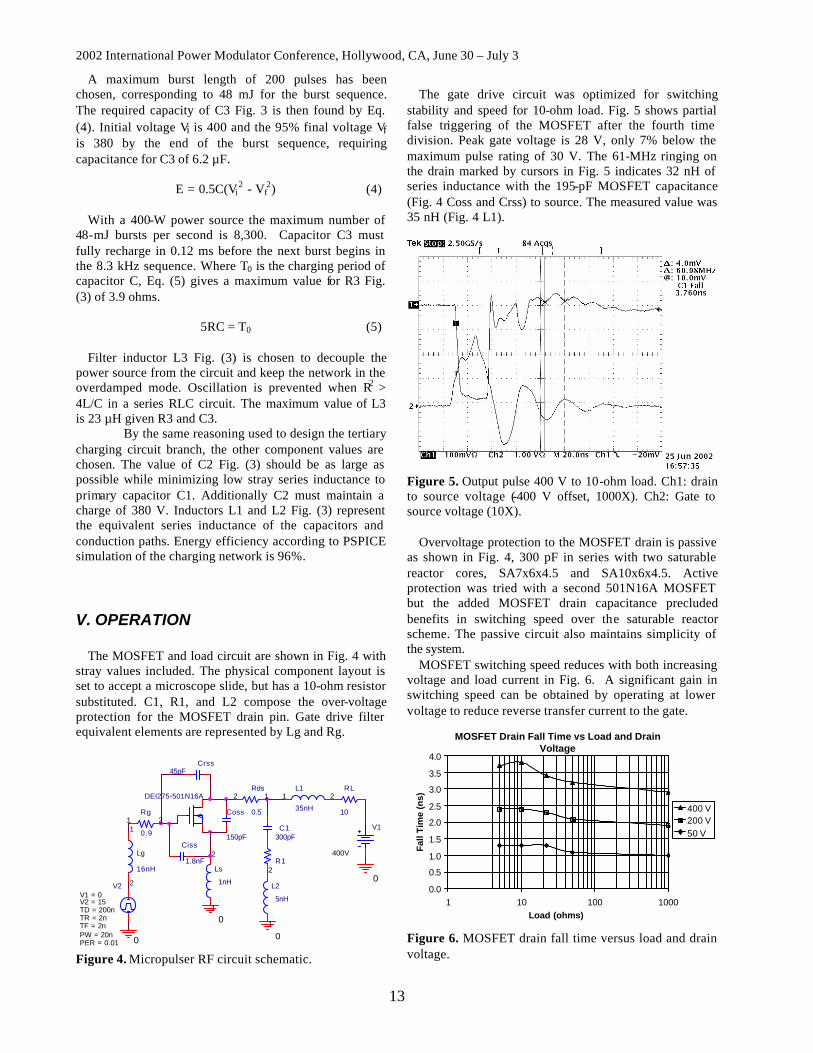
stability and speed for 10-ohm load. Fig. 5 shows partial false triggering of the MOSFET after the fourth time division. Peak gate voltage is 28 V, only 7% below the maximum pulse rating of 30 V. The 61-MHz ringing on the drain marked by cursors in Fig. 5 indicates 32 nH of series inductance with the 195-pF MOSFET capacitance (Fig. 4 Coss and Crss) to source. The measured value was 35 nH (Fig. 4 L1).
Figure 5. Output pulse 400 V to 10-ohm load. Ch1: drain to source voltage (-400 V offset, 1000X). Ch2: Gate to source voltage (10X). Overvoltage protection to the MOSFET drain is passive as shown in Fig. 4, 300 pF in series with two saturable reactor cores, SA7x6x4.5 and SA10x6x4.5. Active protection was tried with a second 501N16A MOSFET but the added MOSFET drain capacitance precluded benefits in switching speed over the saturable reactor scheme. The passive circuit also maintains simplicity of the system. MOSFET switching speed reduces with both increasing voltage and load current in Fig. 6. A significant gain in switching speed can be obtained by operating at lower voltage to reduce reverse transfer current to the gate.
MOSFET Drain Fall Time vs Load and Drain Voltage
0.0
0.5
1.0
1.5
2.0
2.5
3.0
3.5
4.0
1 10 100 1000Load (ohms)
Fal
l Tim
e (n
s)
400 V200 V50 V
Figure 6. MOSFET drain fall time versus load and drain voltage.

2002 International Power Modulator Conference, Hollywood, CA, June 30 – July 3
14
Work continues on sharpening the pulse rise and adding additional dimensions of controllability. Pulse by pulse variability in drain fall time is an additional feature of the micropulser under development.
VI. SUMMARY A micropulser has been constructed with one MOSFET to directly deliver to a microscope slide variable width pulses from 15 ns to DC with amplitude up to 400 V. Design emphasis was placed on compact assembly, simplicity, and flexibility in pulse control. Stability of MOSFET gate drive was accomplished with a saturable reactor filter. Pulses obtained had a rise time of 3.8 ns at 400 V to a 10-ohm load.
VII. REFERENCES [1] S. J. Beebe, P. M. Fox, L. J. Rec, K. Somers, R. H. Stark, and K. H. Schoenbach, “Nanosecond pulsed electric field (nsPEF) effects on cells and tissues: apoptosis induction and tumor growth inhibition,” Pulsed Power Plasma Science, volume (1), pp. 211-215, (2001). [2] M. Gundersen et. al., "Caspase activation and membrane phospholipid translocation in human lymphocytes induced with nanosecond pulsed electric fields," to be published. [3] A. Kuthi, T. Vernier, X. Gu and M. Gundersen, “Compact nanosecond pulse generator for cell electroperturbation experiments,” elsewhere in this conference. [4] G. J. Krausse, “The destructive effects of kelvin leaded packages in high speed, high frequency operation,” Directed Energy, Inc., Fort Collins, CO, Tech. Rep. Doc 9200-0002-1, 1998 [5] “Amorphous magnetic noise suppressors: introduction,” Toshiba America Electronic Components, Inc., Westboro, MA, June, 1994.

2002 International Power Modulator Conference, Hollywood, CA, June 30 – July 3
15
COMPACT NANOSECOND PULSE GENERATOR FOR
CELL ELECTROPERTURBATION EXPERIMENTS∗
Andras Kuthi, Tom Vernier, Xianyue Gu, and Martin Gundersenξ
Department of Electrical Engineering - Electrophysics
University of Southern California Los Angeles, CA 90089-0271
Abstract The design of a compact pulse generator using a Blumlein PFN, is presented. A small Blumlein is utilized to produce high current and high voltage pulses applied to a standard 1mm electroporation cuvette. Alternative designs of the Blumlein are discussed. A MOSFET based resonant charger is also described.
VI. INTRODUCTION Electroperturbation of biological cells can be achieved by the influence of pulsed electric fields. The voltage induced across a cell membrane depends on the pulse length and pulse amplitude. Pulses longer than ~1 µs will charge the outer cell membrane and can lead to the opening of pores, temporary or permanent, the latter usually resulting in cell death [1]. Pulses much shorter than ~1 µs can affect cell nuclei without adversely affecting the outer cell membrane. An interesting effect of pulses of a few ns duration and ~5–10 kV/mm amplitude is triggering of apoptosis or programmed cell death. Generation of large amplitude short pulses generally requires large equipment. This is a consequence of high voltage insulation and the use of transmission line Pulse Forming Networks (PFN) with relatively low dielectric constant [2]. We have undertaken the development of a compact nanosecond pulse generator for the study of short pulse cell electroperturbation using standard 1mm electroporation cuvettes as electrical load. The pulse generator can be placed in close proximity to the biological diagnostic equipment, usually a fluorescence microscope. A different research program attempts
∗ This work was supported by the AFOSR (Contract/Grant #s: F49620-01-1-0387, F49620-01-1-0495, F49620-02-1-0073) and the ARO (Grant # DAAD19-01-1-0698) ξ email: [email protected]
further miniaturization by integrating the experiment with the pulse generator on a microscope slide [3].
VII. PFN DESIGN The pulse generator is expected to deliver pulses of VP = 10 kV peak amplitude and τP = 5 ns duration. In order to simplify interpretation of the data and aid in modeling of the electrical effects on cell constituents the pulse shape is desired to be square, with rise and fall times short compared to the duration. Bursts of up to 100 pulses with pulse repetition rate of 10 kHz are needed. C. Electrical Load The load is a standard electroporation cuvette. The electrode area is 1 cm x 2.5 cm, and the electrode gap is 1 mm. It is filled with a nutrient solution in which the cells are suspended. The water based solution has a resistivity of ρ ~ 500 Ω−cm. The dielectric constant of the solution is close to that of water, ε = 81. The load behaves as a parallel combination of a resistor and a capacitor, with an RC time constant, τL = ρ ε ε0, of approximately ~ 3 ns. This is comparable to the pulse length. The pulse generator is designed to see a load impedance of ZL ~ 20 Ω , so we expect to see some pulse distortion, particularly slowing of the rise and fall times and some droop. The alternative to this is a generator with much lower output impedance and a resistive load added parallel to the cuvette, thereby wasting most of the energy. D. Transmission Line Design The known load characteristics and the desirability of lowest possible voltages suggest the Blumlein PFN configuration switched with a pressurized spark gap (Fig. 1). The Blumlein consists of two identical series connected transmission lines charged to a common voltage. Each individual line has a characteristic impedance half that of the load.
From Charger
Dry Air
Spark Gap
T = 2.5 ns Z = 10
T = 2.5 ns Z = 10
Cuvette 50k +V sense
-V sense
50
50
50k
100
Figure 1. The Blumlein PFN configuration
Electrical length of each transmission line is half the desired output pulse length, T = ½ τP. The physical

2002 International Power Modulator Conference, Hollywood, CA, June 30 – July 3
16
length, LBL, depends on the wave propagation speed in the dielectric medium storing the energy:
ε
τ2
PBL
cL = (1)
Using distilled water (ε = 81) and glycol (ε = 37) mixture as dielectric in an asymmetric stripline configuration we can adjust the dielectric constant, and hence the pulse length, between 4 < τP < 6 ns. The mechanical configuration of the water transmission line is shown in Figure 2.
Water
Teflon
.37
1.00
1.00.13
4.00
4.25
6.00
Figure 2. The asymmetric water stripline. Dimensions are in inches. The characteristic impedance of the water line is primarily determined by the width of the central strip conductor, w = 9.5 mm, and the distance to the bottom ground, d = 3.2 mm. The interelectrode distance is chosen by the breakdown strength of water and the maximum charge voltage. The chosen width of the center electrode produces the desired Z = 10 Ω characteristic impedance. Alternative transmission line configurations are explored as well. Two different versions of microstrip lines on high dielectric constant ceramic substrates were built, and will be tested in the near future. The ceramic microstrips are smaller than the water lines, but less versatile as the dielectric constant, and hence the pulse length cannot be varied. The layout of the K38 (ε = 38) ceramic substrate microstrip is shown in Fig. 3.
BottomTop
1.800
.4002.00
2.00
Ground Plane1 mil Cu.400
.100
Figure 3. Microstrip on K38 ceramic substrate.
VIII. RESONANT CHARGER
The choice of water as dielectric necessitated the use of a relatively fast charger. The circuit diagram of the charger is shown in Fig. 1.
+
50t
1t
1 mH
1500u250Vdc
1
10 x MUR1100E
HVBNC
Vout
FT50B-77 Bead
BNC
VDC in
BNC
IDsense
50BNC
Voutsense
50
Gate in
BNC
IRF7406
50
1k
APT10035JFLL
50k10kV
6 x 4.7n 1 kV mica
7t 77t
K4022E026
100k
Figure 4. Resonant Charger Circuit
Due to flyback mode of operation the circuit is largely immune to transients associated with the discharge of the transmission line. In this mode the primary switching element of the resonant charger is in the off state when the transmission line is discharged. The circuit can charge a 300 pF line to 10 kV in 1.1 µs. This charging time is less than the time constant of distilled water. The maximum repetition rate of the charger is f = 10 kHz, limited only by the size of the primary DC storage capacitor. A. Energy and Power The energy per puls e, Ep, delivered to the load, RL, can be determined from the pulse length, τp, and the pulse amplitude, VL :
pL
LP R
VE τ
2
= , (1)
and the required power, P , is:
ηf
EP p= . (2)
Here, the pulse repetition frequency is f and the efficiency is η. Thus, the charger circuit must deliver approximately EP = 15 mJ per pulse and provide at least P = 300 W of quasicontinuous power. B. Time scales During the charging interval the water insulated transmission line can be represented as a capacitor parallel with a resistor. The capacitance, C, of this combination must store the pulse energy at the peak charging voltage,
2
2
L
p
V
EC = . (3)

2002 International Power Modulator Conference, Hollywood, CA, June 30 – July 3
17
Properly terminated Blumlein output voltage equals the charging voltage, VL = VCH. The parallel equivalent resistance is calculated from the load capacitance and the time constant of the water dielectric, ρεετ 0rW = ,
C
R wτ= . (4)
The permittivity of free space is ε0 = 8.85 pF/m. Resistivity of distilled water is ρ > 1 MΩ-cm and the relative dielectric constant is εr = 81. Thus, the time constant is about 7 µs. Water eventually acquires an ion concentration that lowers its resistivity and time constant. Keeping the charge time, τch = 1.1 µs, much less than the initial τw, ensures several days of operation between water replacements. The maximum allowable charge time defines a maximum inductance, LS, in series with the transmission line. The charging waveform is approximately a quarter period of the resonant circuit formed by this inductance and the load capacitance. This limits the inductance of the secondary winding of the high-voltage transformer,
C
L chS 2
24π
τ≤ . (5)
Each charging cycle begins with the charging of the primary inductance, LP, to the pulse energy plus losses:
2
2
P
PP I
EL
η= . (6)
The time, tR, it takes to ramp the current to this value, IP, depends on the DC power supply voltage, VDC
DC
PPR V
ILt = . (7)
This being the dominant time interval, it sets the absolute maximum repetition rate as well:
PchRt
fττ ++
≤1
. (8)
C. Switch and transformer The time scales above restrict the selection of the switching device. In a Flyback configuration the critical switch transition is turn off. The turn off time must be significantly shorter than the output rise time in order to avoid losses during commutation of the peak switch current. Such turn off losses directly affect the pulse energy, while turn on loss only increases the total power dissipation without affecting the resonant energy transfer. The fast turn off requirement suggests the use of MOSFET for the switching device. The other possible device type, IGBT, generally has much slower turn off times at the high current, high voltage levels this application requires. The selected switch is the APT10035JFLL MOSFET. Its maximum allowable drain voltage is VD = 1 kV, and the maximum pulse current is IP = 100 A. Typical turn off time is 6 ns.
Fast turn off is achieved in practice by using a fast driving circuit. The circuit in Figure 2 shows the driving arrangement. It uses a small, fast, P-channel MOSFET to effectively short the gate to source during the off time and thus eliminate possible turn-on by the fast rising drain voltage coupled to the gate through the drain-gate capacitance. Such unintended turn-on or “shot through” is difficult to avoid with passive drive alone, especially when the ringing from the discharge of the transmission line is reflected back across the MOSFET. The input gate signal swings from –5 V to +10 V. The negative off voltage is important to fully turn on the P-channel MOSFET. The present design proved to be very reliable in this respect and no MOSFET failed in operation. The series gate resistors slow the turn on transition down. This is important, as the energy stored in the primary resonant capacitors placed directly across the drain and source is dissipated in the device at the beginning of each charge period. Fast turn-on results in excessive drain current during the discharge of these capacitors and the device rating can easily be exceeded. In the present circuit the slow turn on eliminates the initial drain current spike. During the Flyback period the switch voltage rises to a maximum, VD, determined by the primary resonant capacitance, CD. It is advantageous to let the primary voltage rise to the limit set by the switch rating, with about 10% safety margin, as this minimizes the turn ratio,
D
L
VV
N 1.1= . (9)
In our case, the turn ratio is N = 11. The primary inductance calculated from Eq. (6) is LP = 3.4 µH, the
secondary inductance from 2NLL PS = is LS = 408 µH.
The secondary inductance satisfies the inequality in Eq. (5). The primary resonant capacitance, from
2NCCD = , is CD = 36 nF. This capacitance needs to be adjusted if the coupling coefficient between the primary and secondary windings of the transformer is different from the optimum value of 64%. The consequences are a small reduction in efficiency, some ringing and modified charge time. In this circuit CD = 33 nF, of which about 3 nF is supplied by the drain-source capacitance of the MOSFET. At the end of the current ramp the energy is stored in the magnetic field of the primary inductance. This field is concentrated in the transformer core. The stored energy divided by the energy density of the magnetic field, BS, in the core indicates the minimum core volume, VC,
2
02
S
PC B
EV
µµ= . (10)
It is clear that to limit the core volume relatively small core permeability, µ, is advantageous. Low permeability also helps to establish the optimum coupling coefficient for efficient resonant energy transfer. Simple separation of the primary and secondary windings, NP and NS turns,

2002 International Power Modulator Conference, Hollywood, CA, June 30 – July 3
18
on different ends of the bobbin is adequate if µ < 100, while external inductance in series with the secondary winding must be used to simulate the leakage inductance if the permeability is high. The minimum core cross section, AC, is given by the flux and the saturation field, BS,
SP
PPC BN
ILA = . (11)
The nickel-iron powder E-core K4022E026 from Magnetics, Inc. has the proper cross section, AC = 2.4 cm2, and volume, VC = 23 cm3. Initial permeability is µ = 26, and the saturation field is BS = 0.5 T.
Layered winding with monotonically decreasing number of turns on each successive layer results in minimum interlayer and interturn capacitance. The primary winding has NP = 7 turns of 18 awg magnet wire placed at one end of the bobbin. The secondary winding is NS = 77 turns of 24 awg magnet wire in four layers, separated from the primary winding by 6 mm. The first layer has 40 turns, the second 20 turns, the third 10 turns and the top layer is the remaining 7 turns. The layers are insulated by Teflon tape. The transformer primary inductance swings between 5.1 µH at the beginning of the current ramp to 3.4 µH at the peak of the current. The effective permeability of the core at 100 A peak current is µ = 18. Due to this swing in inductance the ramp time using VDC = 48 V power supply is approximately τR ~ 10 µs. Estimated temperature rise of the transformer at full power is 32 oC above ambient. D. Sensors Output voltage is sensed by a simple 2000 : 1 voltage divider. The coaxial cable is terminated by 50 Ω at the oscilloscope end. The high voltage resistor is of low inductance type, kept away from nearby ground surfaces. Primary current is sensed by a small 50 : 1 current transformer. It is made of an FT50B-77 ferrite bead, using a single turn primary and 50 turns of 28 awg wire secondary. The secondary is terminated by 1 Ω , resulting in 50 A/V sensitivity.
IX. OPERATION Typical charging pulse into the single water line of 300 pF is shown in Fig. 5.
Figure 5. Charging waveforms. Ch. 1 is primary current, 85 A peak, Ch. 2 is output voltage, 10 kV peak. Problems with the anodization on the aluminum electrodes and excessive conductance prevented full scale operation to date.
X. SUMMARY We have described the design, construction and operation of a compact nanosecond pulse generator.
XI. REFERENCES [1] E. Neumann, A.E. Sowers, and C.A. Jordan, “Electroporation and electrofusion in cell biology” Plenum Press, New York, NY 1989. [2] J. Deng, R.H. Stark, and K.H. Schoenbach, “A Nanosecond Pulse Generator for Intracellular electromanipulation” 24th Int. Power Modulator Symposium, June 26-29, 2000. pages 47-50. [3] M. Behrend, A. Kuthi, T. Vernier, and M. Gundersen, “Micropulser for real-time microscopy of cell electroperturbation“, elsewhere in this conference.
2002 International Power Modulator Conference, Hollywood, CA, June 30 – July 3
19
ULTRASHORT PULSE ELECTROPORATION: APPLICATIONS OF HIGH PULSED ELECTRIC FIELDS TO INDUCED CASPASE ACTIVATION OF HUMAN
LYMPHOCYTES
Martin Gundersen* a, P.Thomas Verniera,d, Laura Marcua,c, Aimin Lib, Xhumei Zhub, Ali Z. Gallama, Thomas Katsouleasa, Clayton Younga , Matthew Behrend, and
Cheryl M. Craftb
a Dept. of Elec. Engineering–Electrophysics, Univ. of Southern California, Los Angeles CA b Mary D. Allen Laboratory for Vision Research, Doheny Eye Institute, Department of Cell and
Neurobiology, Keck School of Medicine, Univ. of Southern California, Los Angeles CA c Biophotonics Res. & Tech. Development, Cedars-Sinai Medical Center, Los Angeles CA
d Information Sciences Institute and MOSIS, University of Southern California
Abstract This paper presents evidence for apoptosis, or programmed cell death, and up-regulation of a subset of important genes induced by intense electric fields of short duration (10’s nsec). The fields are observed to perturb mitochondrial membranes and the compartmentalized intracellular environment of Jurkat T lymphocytes, and within hours caspase activation occurs. Iintense, but low energy, fields can penetrate a biological cell and invoke mechanisms associated with apoptosis.
I. Introduction Pulsed electric fields applied to biological cells and tissue [i,ii,iii], have a wide range of medical applications [iv,v,vi,vii] including drug uptake [viii] and genetic engineering wherein fields and introduced molecules affect DNA within cell nuclei [ix]. Electroporation refers to the phenomena of rearranging the structure of the membrane or membranes of cells to introduce or modify porosity across the membrane film [x] by application of an electric field. Electroporation can provide a mechanism for transport between the extra -cellular and intracellular fluids, and also has important applications for the development of bio-inspired and bio-based devices in understanding the biophysics of cell membranes [xi,xii,xiii,xiv]. The response to a pulsed electric field can be transient, or electroperturbative [xv]. In this paper we explore the production of such perturbative effects by the application of ultra-short intense pulses [xvi], or Ultra-short Pulse Systems Electroperturbation Technology (UPSET). The term electroperturbation is employed to emphasize that the observations reported here, using ultrashort pulses, show perturbative effects on internal organelles at both the proteomic and the genomic levels. This technology offers the possibility of applying very high fields that have nevertheless very low pulse energy, and that when applied under appropriate conditions do not permanently injure or damage normal cell structure or function. The ultrashort pulse exposures described in this paper take place in physiological media, permitting direct observation of the effects of electric pulse perturbations in normal, respiring, fully viable cultured cells. In spite of decades of research, there is an incomplete understanding of the effects of electromagnetic fields within biological cells and tissues [7]. Investigations of pulsed electric fields and microwave radiation aimed at achieving cell effects such as electroporation have historically utilized relatively long pulse lengths (>>1 µsec) and microwave radiation approaching the thermal-heating regime. The approach described here provides a real-time platform for investigations at the cellular and sub-cellular levels, and conclusions drawn from the behavior of these systems have the potential for providing information about the physiological responses of aggregations of cells, tissues, and organs to a range of electric and electromagnetic phenomenon.
*Author to whom correspondence should be addressed: M.C. 0271, Department of Electrical Engineering–Electrophysics, University of Southern California, Los Angeles CA, 90089-0271. [email protected]

2002 International Power Modulator Conference, Hollywood, CA, June 30 – July 3
20
II. Response of Sub-cellular Organelles to Fast-Rising (nsec rise-rate) Electric Fields In order to calculate the electrical response of a cell to a fast-rising, or short electrical pulse, phenomenological data for cell dielectric properties were incorporated as parameters into an electrical circuit model for a cell, and investigated. The analysis, shown schematically in Figure 1, suggests that high frequency, or more precisely, fast-rising pulsed electrical fields will introduce electric fields into the intracellular media of mammalian cells (Figure 1). Further analysis using a more sophisticated code supported and extended these conclusions. Thus, in order to develop an understanding of the distribution and amplitudes of fields within these cells, and to focus the experimental work, several simulations have been developed. The concept is illustrated using simple lumped circuit elements (Fig. 1-a). Circuit parameters for the distribution of current flow for cells, membranes, etc. are estimated and taken from the literature [xvii]. A key result of the simulations is penetration of the intense, but low energy, electric fields to the interior of the cell.For these studies an intracellular organelle was modeled as a small sphere (compared to cell radius) surrounded by a dielectric membrane, typically relative dielectric constant 4, thickness 5 nm[3, 15]. The studies are being extended to intracellular structures comparable in size to the cell (e.g. the nucleus could be half as large as the cell), and structures that are not spheres. Taking realistic models into account could result in electric field and voltage distributions across the cell with significant deviations from models derived with simple spherical assumptions for the intracellular structures. Further, other side effects, such as thermal effects on processes of apoptosis, may modify the cell behavior, or even may become a dominant factor in determining the consequences of electric fields on cell behavior. Based on these arguments it seems necessary to model the cell as realistically as possible. However, the models provided a clear indication of conditions (pulse width, amplitude) under which field will perturb organelles within the cell.
III. Experimental Approach and Apparatus The experiments required preparation of cultured cells (Jurkat T lymphocyte cells in a medium –– cell culture preparations and handling are detailed below), design and fabrication of pulse generator and pulse forming line to couple the pulse generator to cell cuvettes (preserving the electrical pulse rise time and amplitude), treatment of cells in cuvettes. The diagnostics included testing for Annexin V binding, caspase activation, and mitochondria membrane permeation, and a microarray analysis of gene regulation. We first describe pulse generator details and an overview of pulse experimental procedures.
IV. Ultra-Short Pulse Generation Pulse generator characteristics are an important aspect for this work as the pulse duration and amplitude are in ranges that require specialized pulse generation equipment. This is because the pulse characteristics (few nsec pulses, high electric field) require that the design of the pulse generator, matching of transmission line, and matching to the load (typically a cuvette with conductive solution containing cells that act as small capacitors), must be engineered to match with these pulse shapes and pulse characteristics. Detailed electrical design is described elsewhere [xviii]. For initial work a MOSFET-switched, inductive-adding pulse generator utilizing a balanced, coaxial-cable pulse-forming network and spark-gap switch for pulse shortening were used. The pulse generators were designed and assembled at USC, and delivered electrical pulses to biological material in a variety of exposure modes including single-cell, detached-cell suspensions, and layers of cells in culture. The technique for engineering the inductive adding pulse generator allowed application of the short pulses (typ. 5-10kV, 20 nsec) providing at the electrical load (within the cuvette) large amplitude electric fields. This aspect of pulse generation required advanced power modulator design and technology. Commercially available rectangular electroporation cuvettes with 1- and 4-millimeter electrode separations were used to shock dispersed cells in a defined culture media. The cuvette volumes were 75 to several hundred microliters, cell suspension, with cell concentrations up to 2 x 10⁷ cells per milliliter. Apoptosis induction was confirmed by immunoblot analysis of PARP cleavage in a series of 8-, 20- and 50-shock samples at 5 and 24 hrs after shock (Fig. 2). Trypan blue exclusion experiments verified that the plasma membranes of the cells were immediately permeabilized by 20- and 50-shock treatments, with the 50-shock treatment having a stronger effect. Most of the cells in the 50-shock samples were enlarged and lightly stained with Trypan blue at 0 hr after shock, but this morphological change and the permeabilization to Trypan blue were reversible and totally recovered at 2 hrs after shock. Mitochondrial membrane potential was determined by JC-1 staining and flow cytometry analysis of the shocked and unshocked cells as described (xix) at 1 hr after shock. The 50-shock treatment caused mitochondrial membrane depolarization at 1 hr after shock. Whether this is a direct effect of the ultra-short electric shock to the mitochondrial membrane or a symptom of shock-induced apoptosis or a result of other post-shock intracellular dis turbances is under investigation.

2002 International Power Modulator Conference, Hollywood, CA, June 30 – July 3
21
V. Results These experiments have demonstrated that a rapid, dose-dependent induction of apoptosis can be achieved in Jurkat T
lymphocytes by applying a pulsed electric field –– e.g. that apoptosis is induced by the application of short, low energy, intense field electrical pulses. Results supporting these conclusions are based on the following studies that are basic indicators for apoptosis: Annexin V binding to Jurkat cell membranes (Fig. 2) in a dose (shock number)-dependent manner was measured with flow cytometry analysis . Other features demonstrating apoptosis include translocation of the membrane phospholipid phosphatidylserine to the external face of the cytoplasmic membrane.
We have shown that UPSET triggers the cellular stress response indicated by transcription increasing of the AP-1 family of early gene transcription factors only after 1 hr of exposure. Taken together with the 6 hrs of exposure, these data implicate that the ER stress-mediated cell apoptotic pathways are fundamental mechanisms for UPSET exposure. Obviously, UPSET exposure perturbs mitochondrial structures or other intracellular stress sensors. When stress signals are unable to rescue and protect the cells, the apoptotic pathway is triggered. To date, two relatively well-characterized apoptotic pathways are established. The first pathway is mediated by death receptors such as Fas or Tumor Necrosis Factor (TNF) receptor. In the second pathway, Cyt c is released from mitochondria to the cytoplas m in cells exposed to chemotherapeutic drugs, UV irradiation, growth factor withdrawal, or ligation of Fas and TNF receptors. In addition, cross-talk may occur between the death receptor and the mitochondrial apoptotic pathways. In our experiments, both mitochondria and death receptor pathways may contribute to the apoptosis induced by UPSET exposure. Ultrashort, very large amplitude pulses (high power –– but low total energy delivered) extend the reach of the external electric field to the nucleus and the mitochondrial matrix, the nuclear and mitochondrial membranes, and intracellular storage vacuoles and compartments. UPSET-induced perturbations (electroperturbation) of transmembrane electrical potentials and other polarized microstructures may be expected to have both subtle but significant effects, including triggering of specific pathways to induce an apoptotic cascade.
VI. Acknowledgements: This work was made possible by support from the Air Force Office of Scientific Research (Contract/Grant #s F49620-01-1-0387, F49620-01-1-0495) and the Army Research Office (DAAD19-01-1-0698). One of the investigators (TK) acknowledges support from the USDoE (Grant # DE-FG03-92ER40745) and NSF (Grant # PHY-0078715). It is a pleasure to acknowledge contributions by Paul Majoram for work on the biological cell studies, and Josef Yampolsky for design and fabrication of the MOSFET-based inductive adder pulse generator.
2002 International Power Modulator Conference, Hollywood, CA, June 30 – July 3
22
List of Figures
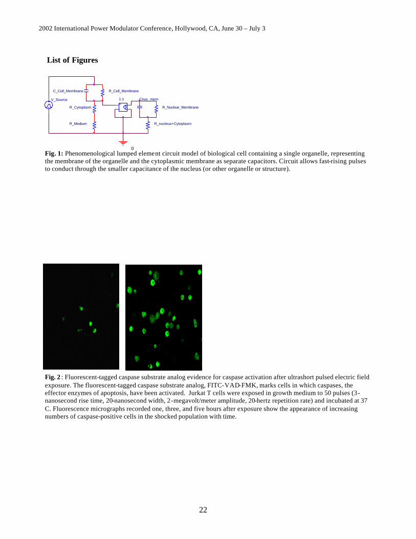
Fig. 1: Phenomenological lumped element circuit model of biological cell containing a single organelle, representing the membrane of the organelle and the cytoplasmic membrane as separate capacitors. Circuit allows fast-rising pulses to conduct through the smaller capacitance of the nucleus (or other organelle or structure).
Fig. 2 : Fluorescent-tagged caspase substrate analog evidence for caspase activation after ultrashort pulsed electric field exposure. The fluorescent-tagged caspase substrate analog, FITC-VAD-FMK, marks cells in which caspases, the effector enzymes of apoptosis, have been activated. Jurkat T cells were exposed in growth medium to 50 pulses (3-nanosecond rise time, 20-nanosecond width, 2-megavolt/meter amplitude, 20-hertz repetition rate) and incubated at 37 C. Fluorescence micrographs recorded one, three, and five hours after exposure show the appearance of increasing numbers of caspase-positive cells in the shocked population with time.
R_Nuclear_Membrane
V_Source
R_nucleus+Cytoplasm
-+
+-
1:1
0
R_Cytoplasm
R_Medium
R_Cell_Membrane
Cnuc_mem
C_Cell_Membrane

2002 International Power Modulator Conference, Hollywood, CA, June 30 – July 3
23
VII. References
[i] See, for example, C. Polk, “Biological Applications of Large Electric Fields: Some History and Fundamentals”, IEEE Trans. Plasma Sci. 28, 1, pp. 6-14, (2000). [ii] J. C. Weaver, “Electroporation of Cells and Tissues,” IEEE Trans. Plasma Science 28 (1) (2000), Weaver, J.C., et al., “Theory of Electroporation: A Review” Elsevier Science Bioelectrochemistry and Bioenergetics 41 (1996) 135-160. [iii] K.R. Foster, “Thermal and Nonthermal Mechanisms of Interaction of Radio-Frequency Energy with Biological Systems”, IEEE Trans. Plasma Sci. 28, pp. 15-23, (2000). [iv] S.B. Dev, D.P. Rabussay, G. Widera, and G.A. Hofmann, “Medical Applications of Electroporation”, IEEE Trans. Plasma Sci. 28, 1, pp. 206-223, (2000). [v] U. Zimmermann, et al., “Electromanipulation of Mammalian Cells: Fundamentals and Application,” IEEE Trans. Plasma Science 28 (1) (2000). See also Lynch, P., et al., “Electrical Manipulation of Cells,” Chapman & Hall (1996). [vi] A.G. Pakhomoc and M.R. Murphy, “Low-Intensity Millimeter Waves as a Novel Therapeutic Modality”, IEEE Trans. Plasma Sci. 28, 1, pp. 34-40 (2000), and references therein. [vii] K. A. DeBruin, et al., “Electroporation and Shock-Induced Transmembrane Potential in a Cardiac Fiber During Defibrillation Strength Shocks,” Annals of Biomedical Engineering 26 (1998) 584-596. See also K. A. DeBruin, et al., “Modeling Electroporation in a Single Cell. II. Effects of Ionic Concentrations,” Biophysical Journal 77 (3) (1999) 1225-1233. [viii] N.F. Chronos, K.A. Robinson, E. Schieffer, N. Crawford, S.B. Dev, G.A. Hofmann, J.E. Brown and S.B. King III, “Enhanced Uptake of Propidium Iodide Marker into Nuclei of SMC in Pig Aorta in vitgro and pig carotid artery in vivo, by direct vessel wall electroporation,” Proc. Cleveland Clinc found. Restenosis Summit VII, p. 32, (1995). [ix] T. Muramatsu, A. Nakamura, and H.M. Park, “in vivo electroporation: A Powerful and Convenient Means of Non Viral Gene Transfer to Tissues of Living Animals,” Int. J. Mol. Med., 1, pp. 55-62 (1998). [x] U. Zimmerman, Electromanipulation of Cells . Boca Raton FL: CRC Press, 1996. [xi] T. Vernier, X. Zhu, C. Craft, L. Marcu M. Gundersen, in preparation. [xii] E. Neumann, et al., “Electroporation and Electrofusion in Cell Biology,” Plenum Press (1989). [xiii] M. Bier, et al., “Kinetics of Sealing for Transient Electropores in Isolated Mammalian Skeletal Muscle Cells,” Bioelectromagnetics 20 (1999) 194-201. [xiv] S. Gabriel, S.R.W. Lau, and C. Gabriel, “The Dielectric Properties of Biological Tissues.2. Masurements in the Frequency Range 10Hz to 20 GHz”, Physics in Medicine and Biology, 41, 11, pp. 2251-2269 (1996). [xv] Schoenbach KH, Beebe SJ, Buescher ES. 2001. Intracellular effect of ultrashort electrical pulses . Bioelectromagnetics. 22(6):440-448. [xvi] R.P. Joshi and K.H. Schoenbach, “Electroporation Dynamics in Biological Cells Subjected to Ultrafast Electrical Pulses: A Numerical Simulation Study,” Phys. Rev. E 62, 1, pp. 1025-1033 (2000). [xvii] See, for example Kotnik, T., and D. Miklavcic. 2000. “Theoretical evaluation of the distributed power dissipation in biological cells exposed to electric fields”, Bioelectromagnetics 21:385-394; DeBruin, K. A., and W. Krassowska. 1999, “Modeling electroporation in a single cell. I. Effects of field strength and rest potential”, Biophysical Journal 77:1213-1224; Joshi, R. P., and K. H. Schoenbach. 2000, “Electroporation dynamics in biological cells subjected to ultrafast electrical pulses: a numerical simulation study”, Physical Review E 62:1025-1033; Marszalek, P., D.-S. Liu, and T. Y. Tsong. 1990, “Schwan equation and transmembrane potential induced by alternating electric field”, Biophysical Journal 58:1053-1058; and Freeman, S. A., M. A. Wang, and J. C. Weaver. 1994, “Theory of electroporation of planar bilayer membranes: predictions of the aqueous area, change in capacitance, and pore-pore separation”, Biophysical Journal 67:42-56. [xviii] Proc. IEEE Power Modulator Conference (to appear). [xix] Cossarizza A, Salvioli S. 2001. Analysis of mitochondria during cell death. Methods Cell Biol . 63:467-486.

2002 International Power Modulator Conference, Hollywood, CA, June 30 – July 3
24
COMPACT NANOSECOND PULSE GENERATOR FOR
PSEUDOSPARK BASED PULSE GENERATOR FOR CORONA ASSISTED COMBUSTION EXPERIMENTS∗
Andras Kuthi, Jianbang Liu, Clayton Young, and Martin Gundersen ξ Department of Electrical Engineering - Electrophysics
University of Southern California Los Angeles, CA 90089-0271
Abstract The design and operation of a pulse generator using an advanced Pseudospark device is presented. An application – corona assisted flame ignition and combustion – is discussed requiring operation of the pseudospark switch at 30 kV charging voltage and up to 100 Hz repetition rate. The pulse generator is comprised of a single stage lumped element Blumlein and 1:3 pulse transforme r designed to produce 50 ns wide pulses with 70 kV peak amplitude. Details of the pseudospark operation are presented.
I. INTRODUCTION Corona discharge assisted flame ignition has interesting properties. Pulsed corona discharge usually consists of many streamers, efficiently filling the gas volume [1]. The plasma produced by the streamers contains ~10 eV electrons, while sparks only produce ~1 eV average electron energy [2]. Compared to conventional spark ignition flames ignited by short pulse corona discharge have shorter delay time, faster pressure rise time, higher maximum pressure and more complete combustion [3,4,5]. Desired pulse amplitude depends on the exact geometry of the combustion chamber and corona electrode. In our case at least 50 kV is needed for efficient energy deposition. The pulse length must be longer than the streamer formation time but shorter than the arc formation time [7]. In the present experiment it is estimated, that the optimum pulse length is between 30 and 70 ns. The pseudospark is a glow-discharge switch that is an extrapolation of thyratron technology, using a different emission process than a traditional externally heated cathode. It is well suited for the present application due to the high peak current capability, relatively high repetition rate and long life. For reviews see [8,9,10,11].
II. DESIGN The pulse generator is expected to deliver pulses of VP = 70 kV peak amplitude and τP = 50 ns duration. Bursts of 100 pulses with pulse repetition rate of 1 - 100 Hz are needed for the present experiments. The rise time, repetition rate, and reliability requirements can be met using pseudospark switch. The final pulse amplitude is achieved by using a pulse transformer. A. Electrical Load The load is a coaxial combustion chamber. The center corona electrode is positive and the chamber wall is at ground potential. Previous experiments indicate that the corona discharge impedance is approximately 250 Ω , sharply dropping to < 100 Ω when streamers reach the opposite electrode and an arc forms [3]. In order to extinguish occasional arcs, the output impedance of the generator should be matched to the load, so peak currents are limited to twice the operating current. The pulse shape is relatively unimportant, as long as the rise time is short and there are no significant oscillations or ringing.

2002 International Power Modulator Conference, Hollywood, CA, June 30 – July 3
25
B. Pulse Forming Network The known load characteristics and the desirability of lowest possible turn ratio for the pulse transformer suggest the lumped element Blumlein PFN configuration (Fig. 2). Ordinarily, a Blumlein pulse forming network consists of two identical series connected transmission lines charged to a common voltage. Each individual line has a characteristic impedance half that of the load. Placing the two lines above each other and recognizing that the lower half of the top line is at the same potential as the upper half of the bottom line, we get the simplified diagram shown on Figure 1.
Z, T
Z, T
2 Z
VDC
V = VDC
LC
CL
CL / 2
C
Figure 1. Synthesis of the lumped element Blumlein Unfortunately, L-C circuits do not combine as cleanly as transmission lines [4]. The ideal output pulse from the transmission lines is a square pulse with length twice the single line delay. On the other hand, the ideal – i.e. shortest possible non-ringing – output pulse from a single L-C circuit is a critically damped pulse. The peak amplitude of such a pulse is ~ 64% of the charging voltage. The combination of the two L-C circuits will not produce a non-ringing pulse unless the capacitor values are adjusted. The actual values of the capacitors shown in Fig. 2 give a good pulse (Fig. 3) with shortest rise and fall times into a resistive load of 12 Ω .
To Heater PS
3500
33k
1n
1n
50k
-2 kV
1.3 mA
-4 kV trig
FS2000
4 nF
1
+30 kV DC in
500k
500k
PSEUDOSPARK Combustion chamber
Corona electrode
Pressure
Gas in
Metglas core
35 nH
2 nF
12
Figure 2. The corona assisted combustion experiment The inductor in the circuit is formed by the combined inductance of the pseudospark switch arc channel and the connecting 16 awg wire to the capacitor midpoint. This arrangement results in the shortest possible pulse. The capacitors can be reduced further and the pulse shortened if the load impedance can increase. Unfortunately, the pulse transformer leakage inductance introduces severe ringing in the absence of the 12 Ω primary load resistance, so we could not take this approach. An optimized pulse transformer may allow further reduction in the pulse length.
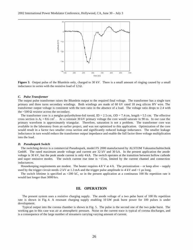
2002 International Power Modulator Conference, Hollywood, CA, June 30 – July 3
26
Figure 3. Output pulse of the Blumlein only, charged to 30 kV. There is a small amount of ringing caused by a small inductance in series with the resistive load of 12 Ω . C. Pulse Transformer The output pulse transformer raises the Blumlein output to the required final voltage. The transformer has a single turn primary and three turns secondary windings. Both windings are made of 60 kV rated 18 awg silicon HV wire. The transformer output voltage is consistent with the turn ratio in the absence of a load. The voltage ratio drops to 2.4 with the ~500 Ω resistor across the secondary. The transformer core is a metglas-polyethylene-foil toroid, ID = 2.5 cm, OD = 7.4 cm, length = 5.5 cm. The effective cross section is AC = 8.6 cm2. . At a constant 30 kV primary voltage the core would saturate in 90 ns. In our case the primary waveform is approximately triangular. Therefore, saturation is not a problem. The transformer core was available in the laboratory from an earlier project, and was not optimized to this application. Optimization of the core would result in a factor two smaller cross section and significantly reduced leakage inductance. The smaller leakage inductance in turn would reduce the transformer output impedance and enable the full factor three voltage multiplication into the load. D. Pseudospark Switch The switching device is a commercial Pseudospark, model FS 2000 manufactured by ALSTOM Vakuumschalttechnik GmbH. The rated maximum anode voltage and current are 32 kV and 30 kA. In the present application the anode voltage is 30 kV, but the peak anode current is only 4 kA. The switch operates at the transition between hollow cathode and super emissive modes. The switch current rise time is ~15 ns, limited by the current channel and connection inductances. Housekeeping requirements are modest. The heater requires 4.8 V at 4 A. The preionization – or keep alive – supply used by the trigger circuit needs -2 kV at 1.3 mA and the trigger pulse amplitude is -4 kV and >1 µs long. The switch lifetime is specified as >200 kC, so in the present application at a continuous 100 Hz repetition rate it would last longer than 3000 hrs.
III. OPERATION The present system uses a resistive charging supply. The anode voltage of a two pulse burst of 100 Hz repetition rate is shown in Fig. 4. A resonant charging supply enabling 10 kW peak burst power for 100 pulses is under development. Typical output into the corona chamber is shown in Fig. 5. The pulse is the second one of the two pulse burst. The working gas in this case was air at atmospheric pressure. Noise on the current trace is typical of corona discharges, and is a consequence of the large number of streamers carrying varying amount of current.

2002 International Power Modulator Conference, Hollywood, CA, June 30 – July 3
27
Figure 4. Anode voltage of two pulse burst at 100 Hz repetition rate
Figure 5. Typical load voltage and current. Ch. 1 is current, 100 A/div. Ch. 2 is voltage, 10 kV/div. PFN is charged to 25 kV. Output voltage is sensed by a commercial 1000:1 HV probe. Load current is measured by a Pearson 411 current transformer. Due to relatively slow rise time of this transformer (20 ns) the current signal is only qualitative. A fast current transformer is being designed at present and will be used for precise energy deposition measurements.
IV. SUMMARY We have described the design, construction and operation of a pseudospark based pulse generator. Reliable long life operation is made possible by the pseudospark switch.

2002 International Power Modulator Conference, Hollywood, CA, June 30 – July 3
28
V. REFERENCES [1] E.M. Bazeluan, and Yu.P. Raizer, “Spark discharge”, CRC Press, Boca Raton, New York, 1997. [2] Y.L.W. Creyghton, “Pulsed positive corona discharges”, 1990. [3] V. Puchkarev and M. Gundersen, "Energy efficient plasma processing of gaseous emission using short pulses," Appl. Phys. Lett. 71 (23), 3364 (1997). [4] J.B. Liu, P.D. Ronney, and M.A. Gundersen, “Premixed flame ignition by pulsed corona discharges“ , Western States Meeting of The Combustion Institute, 2002 Spring, San Diego, CA. [5] M. Gundersen, V. Puchkarev, and G. Roth, “Transient plasma for environment applications with low energy cost,” 1998 IEEE International Conference on Plasma Science, Raleigh, NC, June 1-4, 1998. [6] Ian D. Smith, “A novel voltage multiplication scheme using transmission lines” Proc. 15th IEEE Power Modulator Symposium, 223-226, (1982). [7] V. Puchkarev and M. Gundersen, “Power modulators for control of transient plasmas for environmental applications,” 23rd International Power Modulator Symposium, Rancho Mirage, CA June 22-25, 1998. [8] K. Frank, E. Boggasch, J. Christiansen, A. Goertler, W. Hartmann, C. Kozlik, G. Kirkman, C. G. Braun, V. Dominic, M.A. Gundersen, H. Riege and G. Mechtersheimer, "High power pseudospark and BLT switches," IEEE Trans. Plasma Science 16 (2), 317 (1988). [9] "The Physics and Applications of Pseudosparks," NATO ASI Series B 219, Plenum Press (1990) [10] G. Kirkman-Amemiya, H. Bauer, R. L. Liou, T. Y. Hsu, H. Figueroa, and M. A. Gundersen, "A study of the high-current back-lighted thyratron and pseudospark switch," Proceedings of the Nineteenth Power Modulator Symposium, 254 (1990). [11] M. Gundersen and G. Roth, “High power switches,” in “The Handbook of Accelerator Physics and Engineering,” Eds. A. Chao and Maury Tigner, World Scientific Publishing Co. (1999).