comparison between arm amba protocols and verification of
TRANSCRIPT
International Research Journal of Engineering and Technology (IRJET) e-ISSN: 2395-0056
Volume: 08 Issue: 06 | June 2021 www.irjet.net p-ISSN: 2395-0072
© 2021, IRJET | Impact Factor value: 7.529 | ISO 9001:2008 Certified Journal | Page 3395
Comparison between ARM AMBA Protocols and Verification of APB
Protocol Using System Verilog & UVM
Soumya Rai1, Virendra Pratap Yadav2
1M. Tech, Dept. of ECE, SHEAT College of Engineering and Management, Varanasi, India 2Associate Professor, Dept. of ECE, SHEAT College of Engineering and Management, Varanasi, India
---------------------------------------------------------------------***---------------------------------------------------------------------
Abstract - Increasing technology increases the amount of logic that can be placed on a silicon chip, resulting in the development of highly integrated SoC (System on Chip) designs. The most important aspect of a SoC is how well it is interconnected. An on-chip bus architecture is used by the SoC. The AMBA (Advanced Microcontroller Bus Architecture) bus is the most widely used on-chip bus introduced by ARM. Almost 85-90 percent of any SoC's on-chip bus is AMBA (Advanced Microcontroller Bus Architecture). The most commonly used AMBA protocols for on-chip communication are APB, AHB, and AXI in the form of an AHB/AXI to APB bridge, with AHB and AXI interfacing high bandwidth peripherals and APB interfacing low bandwidth peripherals. Pipelining, burst, and split transfers are among the advanced features included in these protocols. In this paper, we describe a case study for various AMBA SOC bus protocols and compare their performance: AMBA (Advanced Microcontroller Bus Architecture) protocols A verification environment of the AMBA APB protocol using the System Verilog language and the Universal Verification Methodology is simulated using the Aldec Riviera Pro simulator, which is freely available on the EDA playground. This paper begins with a brief overview of the AMBA 2.0 protocol, AMBA 3.0 protocol, and AMBA 4.0 protocol, and concludes with a discussion of a performance comparison analysis of all three AMBA bus protocols with APBand AXI protocol simulation results.
Key Words: SoC, AMBA, AXI, APB, AHB, UVM, System Verilog. 1.INTRODUCTION
Advanced Micro Controller Bus Architecture (AMBA) Bus Protocols is a collection of ARM interconnecting specifications that standardise chip communication mechanisms between different functional blocks (or IP) for building high-performance SOC designs. Usually, these designs include one or more microcontrollers or microprocessors together with a variety of other components—internal memory or external memory bridge, DSP, DMA, accelerators and various other peripherals such as USB, UART, PCIE, I2C, etc [1]. All incorporated on a single chip. The main incentive of AMBA protocols is to provide a standard and efficient way of interconnecting these blocks with re-use across multiple designs.
In recent years due to the growing market conditions for low-power, a minimum area with lowest engineering cost and high-performance systems, as well as the enhancement of semiconductor process technology, the demand for Very Large-Scale Integration (VLSI) increased to the point that all
device components are expected to be integrated into a single chip called a System on chip (SoC). These intellectual property (IPs) with different features are inserted into a chip, and all of these IP modules may have completed their design and verification separately. However, several scenarios are posed unexpectedly with the individual IPs, and thus the whole SoC can lead to failure. Incompatibility between IP interfaces causes a common transaction error problem. Thus, for the implementation of any System on chip (SoC) it has become a rule that the standardised and pre-tested bus protocol interface architecture should be integrated. So on-chip communication using a bus protocol, the specification of which provides a standard interface that facilitates IP integration, has become the basis of the SoC architecture. Some of the standards for bus-based communication architecture have been set over the past few years in order to facilitate the reusability of IPs and to achieve SoC convergence in time.
1.1. EVOLUTION OF AMBA PROTOCOL
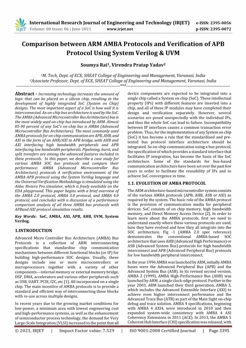
The ARM architecture-based microcontroller system consists of the various AMBA protocols (APB, AHB, ASB or AXI) as required by the system. The basic role of the AMBA protocol is the provision of communication media for peripheral devices. SoC consists of on chip memory, high bandwidth memory, and Direct Memory Access Device [2]. In order to learn more about the AMBA protocols, first we need to understand exactly where these various protocols are used, how they have evolved and how they all integrate into the SOC architecture. Fig -1 (AMBA 2.0 spec reference) demonstrates the conventional AMBA-based SOC architecture that uses AHB (Advanced High Performance) or ASB (Advanced System Bus) protocols for high bandwidth interconnect and APB (Advanced Peripheral Bus) protocols for low bandwidth peripheral interconnect.
In the year 1996 AMBA was launched by ARM, initially AMBA buses were the Advanced Peripheral Bus (APB) and the Advanced System Bus (ASB). In its revised second version, AMBA 2 (1999), AMBA High-Performance Bus (AHB) was launched by ARM, a single clock-edge protocol. Further in the year 2003, ARM launched their third generation, AMBA 3, which includes the Advanced Extensible Interface (AXI) to achieve even higher interconnect performance and the Advanced Trace Bus (ATB) as part of the Main Sight on-chip debug and trace solution. AMBA 4 specifications, beginning with AMBA 4 AXI4, were introduced in 2010 and then expanded system-wide consistency with AMBA 4 AXI Coherency Extensions in 2011 (ACE). In 2013, the AMBA 5 Coherent Hub Interface (CHI) specification was released, with
International Research Journal of Engineering and Technology (IRJET) e-ISSN: 2395-0056
Volume: 08 Issue: 06 | June 2021 www.irjet.net p-ISSN: 2395-0072
© 2021, IRJET | Impact Factor value: 7.529 | ISO 9001:2008 Certified Journal | Page 3396
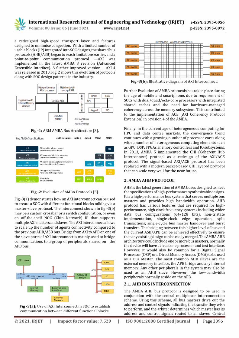
a redesigned high-speed transport layer and features designed to minimise congestion. With a limited number of usable blocks (IP) integrated into SOC designs, the shared bus protocols (AHB/ASB) began to reach limitations earlier, and a point-to-point communication protocol —AXI was implemented in the latest AMBA 3 revision (Advanced Extensible Interface). A further improved version —AXI 4 was released in 2010. Fig. 2 shows this evolution of protocols along with SOC design patterns in the industry.
Fig -1: ARM AMBA Bus Architecture [3].
Fig -2: Evolution of AMBA Protocols [5].
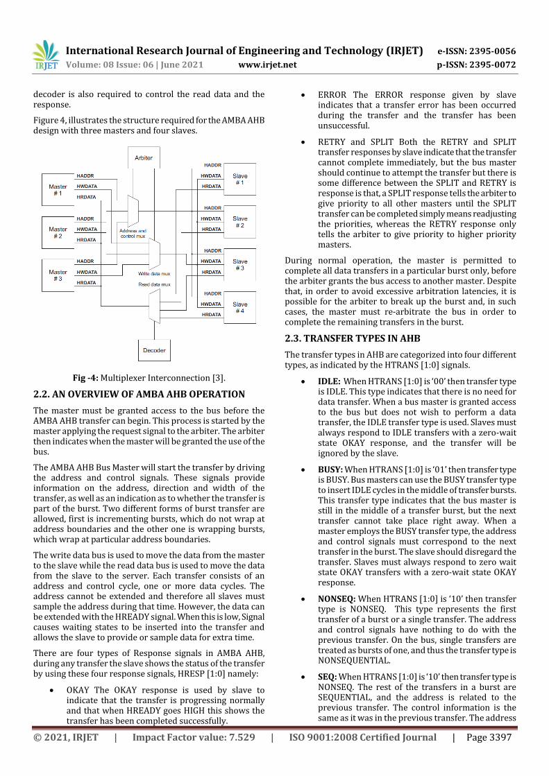
Fig -3(a) demonstrates how an AXI interconnect can be used to create a SOC with different functional blocks talking via a master-slave protocol. The interconnect shown in fig -3(b) may be a custom crossbar or a switch configuration, or even an off-the-shelf NOC (Chip Network) IP that supports multiple AXI masters and slaves. The AXI interconnect allows to scale up the number of agents connectivity compared to the previous AHB/ASB bus. Bridge from AXI to APB on one of the slave ports of AXI interconnect is mainly used to bridge communications to a group of peripherals shared on the APB bus.
Fig -3(a): Use of AXI Interconnect in SOC to establish communication between different functional blocks.
Fig -3(b): Illustrative diagram of AXI Interconnect.
Further Evolution of AMBA protocols has taken place during the age of mobile and smartphone, due to requirement of SOCs with dual/quad/octa-core processors with integrated shared caches and the need for hardware-managed coherency across the memory subsystem. This contributed to the implementation of ACE (AXI Coherency Protocol Extension) in revision 4 of the AMBA.
Finally, in the current age of heterogeneous computing for HPC and data centre markets, the convergence trend continues with a growing number of processor cores along with a number of heterogeneous computing elements such as GPU, DSP, FPGAs, memory controllers and IO subsystems. In 2013, AMBA 5 implemented the CHI (Coherent Hub Interconnect) protocol as a redesign of the AXI/ACE protocol. The signal-based AXI/ACE protocol has been replaced with a modern packet-based CHI layered protocol that can scale very well for the near future. 2. AMBA AHB PROTOCOL
AHB is the latest generation of AMBA buses designed to meet the specifications of high-performance synthesizable designs. It is a high-performance bus system that serves multiple bus masters and provides high bandwidth operation. AHB protocol has various features that are required for high-performance, high clock frequency systems including wider data bus configurations (64/128 bits), non-tristate implementation, single-clock edge operation, split transactions, single-cycle bus master handover and burst transfers. The bridging between this higher level of bus and the current ASB/APB can be achieved effectively to ensure that any existing design can be easily merged. The AMBA AHB architecture could include one or more bus masters, normally the device will have at least one processor and test interface. However, it would also be common for a Digital Signal Processor (DSP) or a Direct Memory Access (DMA) to be used as a Bus Master. The most common AHB slaves are the external memory interface, the APB bridge and any internal memory. Any other peripherals in the system may also be used as an AHB slave. However, the low-bandwidth peripherals normally reside on the APB.
2.1. AHB BUS INTERCONNECTION
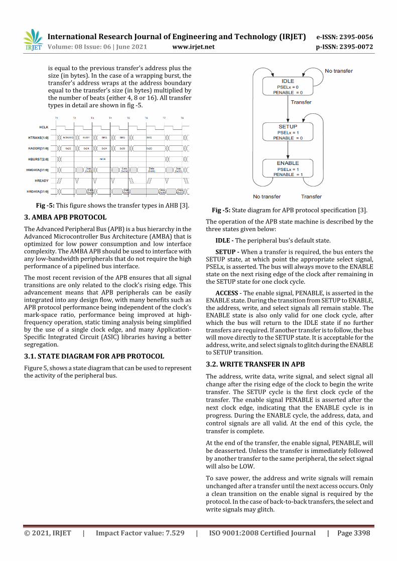
The AMBA AHB bus protocol is designed to be used in conjunction with the central multiplexor interconnection scheme. Using this scheme, all bus masters drive out the address and control signals indicating the transfer they wish to perform, and the arbiter determines which master has its address and control signals routed to all slaves. Central
International Research Journal of Engineering and Technology (IRJET) e-ISSN: 2395-0056
Volume: 08 Issue: 06 | June 2021 www.irjet.net p-ISSN: 2395-0072
© 2021, IRJET | Impact Factor value: 7.529 | ISO 9001:2008 Certified Journal | Page 3397
decoder is also required to control the read data and the response.
Figure 4, illustrates the structure required for the AMBA AHB design with three masters and four slaves.
Fig -4: Multiplexer Interconnection [3].
2.2. AN OVERVIEW OF AMBA AHB OPERATION
The master must be granted access to the bus before the AMBA AHB transfer can begin. This process is started by the master applying the request signal to the arbiter. The arbiter then indicates when the master will be granted the use of the bus.
The AMBA AHB Bus Master will start the transfer by driving the address and control signals. These signals provide information on the address, direction and width of the transfer, as well as an indication as to whether the transfer is part of the burst. Two different forms of burst transfer are allowed, first is incrementing bursts, which do not wrap at address boundaries and the other one is wrapping bursts, which wrap at particular address boundaries.
The write data bus is used to move the data from the master to the slave while the read data bus is used to move the data from the slave to the server. Each transfer consists of an address and control cycle, one or more data cycles. The address cannot be extended and therefore all slaves must sample the address during that time. However, the data can be extended with the HREADY signal. When this is low, Signal causes waiting states to be inserted into the transfer and allows the slave to provide or sample data for extra time.
There are four types of Response signals in AMBA AHB, during any transfer the slave shows the status of the transfer by using these four response signals, HRESP [1:0] namely:
OKAY The OKAY response is used by slave to indicate that the transfer is progressing normally and that when HREADY goes HIGH this shows the transfer has been completed successfully.
ERROR The ERROR response given by slave indicates that a transfer error has been occurred during the transfer and the transfer has been unsuccessful.
RETRY and SPLIT Both the RETRY and SPLIT transfer responses by slave indicate that the transfer cannot complete immediately, but the bus master should continue to attempt the transfer but there is some difference between the SPLIT and RETRY is response is that, a SPLIT response tells the arbiter to give priority to all other masters until the SPLIT transfer can be completed simply means readjusting the priorities, whereas the RETRY response only tells the arbiter to give priority to higher priority masters.
During normal operation, the master is permitted to complete all data transfers in a particular burst only, before the arbiter grants the bus access to another master. Despite that, in order to avoid excessive arbitration latencies, it is possible for the arbiter to break up the burst and, in such cases, the master must re-arbitrate the bus in order to complete the remaining transfers in the burst.
2.3. TRANSFER TYPES IN AHB
The transfer types in AHB are categorized into four different types, as indicated by the HTRANS [1:0] signals.
IDLE: When HTRANS [1:0] is ‘00’ then transfer type is IDLE. This type indicates that there is no need for data transfer. When a bus master is granted access to the bus but does not wish to perform a data transfer, the IDLE transfer type is used. Slaves must always respond to IDLE transfers with a zero-wait state OKAY response, and the transfer will be ignored by the slave.
BUSY: When HTRANS [1:0] is ‘01’ then transfer type is BUSY. Bus masters can use the BUSY transfer type to insert IDLE cycles in the middle of transfer bursts. This transfer type indicates that the bus master is still in the middle of a transfer burst, but the next transfer cannot take place right away. When a master employs the BUSY transfer type, the address and control signals must correspond to the next transfer in the burst. The slave should disregard the transfer. Slaves must always respond to zero wait state OKAY transfers with a zero-wait state OKAY response.
NONSEQ: When HTRANS [1:0] is ‘10’ then transfer type is NONSEQ. This type represents the first transfer of a burst or a single transfer. The address and control signals have nothing to do with the previous transfer. On the bus, single transfers are treated as bursts of one, and thus the transfer type is NONSEQUENTIAL.
SEQ: When HTRANS [1:0] is ‘10’ then transfer type is NONSEQ. The rest of the transfers in a burst are SEQUENTIAL, and the address is related to the previous transfer. The control information is the same as it was in the previous transfer. The address
International Research Journal of Engineering and Technology (IRJET) e-ISSN: 2395-0056
Volume: 08 Issue: 06 | June 2021 www.irjet.net p-ISSN: 2395-0072
© 2021, IRJET | Impact Factor value: 7.529 | ISO 9001:2008 Certified Journal | Page 3398
is equal to the previous transfer's address plus the size (in bytes). In the case of a wrapping burst, the transfer's address wraps at the address boundary equal to the transfer's size (in bytes) multiplied by the number of beats (either 4, 8 or 16). All transfer types in detail are shown in fig -5.
Fig -5: This figure shows the transfer types in AHB [3].
3. AMBA APB PROTOCOL
The Advanced Peripheral Bus (APB) is a bus hierarchy in the Advanced Microcontroller Bus Architecture (AMBA) that is optimized for low power consumption and low interface complexity. The AMBA APB should be used to interface with any low-bandwidth peripherals that do not require the high performance of a pipelined bus interface.
The most recent revision of the APB ensures that all signal transitions are only related to the clock's rising edge. This advancement means that APB peripherals can be easily integrated into any design flow, with many benefits such as APB protocol performance being independent of the clock's mark-space ratio, performance being improved at high-frequency operation, static timing analysis being simplified by the use of a single clock edge, and many Application-Specific Integrated Circuit (ASIC) libraries having a better segregation.
3.1. STATE DIAGRAM FOR APB PROTOCOL
Figure 5, shows a state diagram that can be used to represent the activity of the peripheral bus.
Fig -5: State diagram for APB protocol specification [3].
The operation of the APB state machine is described by the three states given below:
IDLE - The peripheral bus's default state.
SETUP - When a transfer is required, the bus enters the SETUP state, at which point the appropriate select signal, PSELx, is asserted. The bus will always move to the ENABLE state on the next rising edge of the clock after remaining in the SETUP state for one clock cycle.
ACCESS - The enable signal, PENABLE, is asserted in the ENABLE state. During the transition from SETUP to ENABLE, the address, write, and select signals all remain stable. The ENABLE state is also only valid for one clock cycle, after which the bus will return to the IDLE state if no further transfers are required. If another transfer is to follow, the bus will move directly to the SETUP state. It is acceptable for the address, write, and select signals to glitch during the ENABLE to SETUP transition.
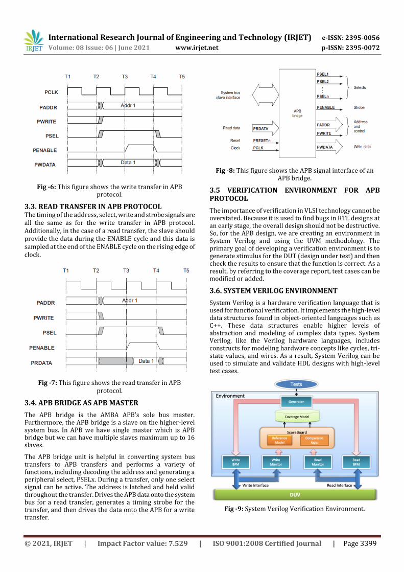
3.2. WRITE TRANSFER IN APB
The address, write data, write signal, and select signal all change after the rising edge of the clock to begin the write transfer. The SETUP cycle is the first clock cycle of the transfer. The enable signal PENABLE is asserted after the next clock edge, indicating that the ENABLE cycle is in progress. During the ENABLE cycle, the address, data, and control signals are all valid. At the end of this cycle, the transfer is complete.
At the end of the transfer, the enable signal, PENABLE, will be deasserted. Unless the transfer is immediately followed by another transfer to the same peripheral, the select signal will also be LOW.
To save power, the address and write signals will remain unchanged after a transfer until the next access occurs. Only a clean transition on the enable signal is required by the protocol. In the case of back-to-back transfers, the select and write signals may glitch.
International Research Journal of Engineering and Technology (IRJET) e-ISSN: 2395-0056
Volume: 08 Issue: 06 | June 2021 www.irjet.net p-ISSN: 2395-0072
© 2021, IRJET | Impact Factor value: 7.529 | ISO 9001:2008 Certified Journal | Page 3399
Fig -6: This figure shows the write transfer in APB protocol.
3.3. READ TRANSFER IN APB PROTOCOL The timing of the address, select, write and strobe signals are all the same as for the write transfer in APB protocol. Additionally, in the case of a read transfer, the slave should provide the data during the ENABLE cycle and this data is sampled at the end of the ENABLE cycle on the rising edge of clock.
Fig -7: This figure shows the read transfer in APB protocol.
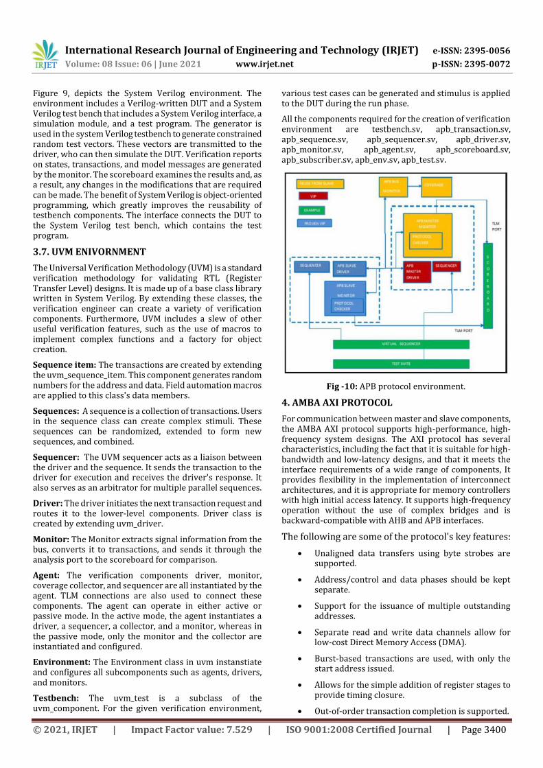
3.4. APB BRIDGE AS APB MASTER
The APB bridge is the AMBA APB’s sole bus master. Furthermore, the APB bridge is a slave on the higher-level system bus. In APB we have single master which is APB bridge but we can have multiple slaves maximum up to 16 slaves.
The APB bridge unit is helpful in converting system bus transfers to APB transfers and performs a variety of functions, including decoding the address and generating a peripheral select, PSELx. During a transfer, only one select signal can be active. The address is latched and held valid throughout the transfer. Drives the APB data onto the system bus for a read transfer, generates a timing strobe for the transfer, and then drives the data onto the APB for a write transfer.
Fig -8: This figure shows the APB signal interface of an APB bridge.
3.5 VERIFICATION ENVIRONMENT FOR APB PROTOCOL
The importance of verification in VLSI technology cannot be overstated. Because it is used to find bugs in RTL designs at an early stage, the overall design should not be destructive. So, for the APB design, we are creating an environment in System Verilog and using the UVM methodology. The primary goal of developing a verification environment is to generate stimulus for the DUT (design under test) and then check the results to ensure that the function is correct. As a result, by referring to the coverage report, test cases can be modified or added.
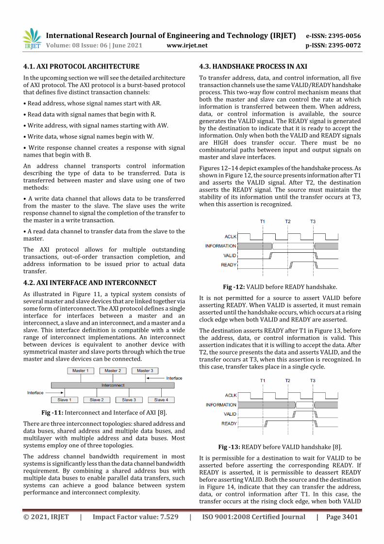
3.6. SYSTEM VERILOG ENVIRONMENT
System Verilog is a hardware verification language that is used for functional verification. It implements the high-level data structures found in object-oriented languages such as C++. These data structures enable higher levels of abstraction and modeling of complex data types. System Verilog, like the Verilog hardware languages, includes constructs for modeling hardware concepts like cycles, tri-state values, and wires. As a result, System Verilog can be used to simulate and validate HDL designs with high-level test cases.
Fig -9: System Verilog Verification Environment.
International Research Journal of Engineering and Technology (IRJET) e-ISSN: 2395-0056
Volume: 08 Issue: 06 | June 2021 www.irjet.net p-ISSN: 2395-0072
© 2021, IRJET | Impact Factor value: 7.529 | ISO 9001:2008 Certified Journal | Page 3400
Figure 9, depicts the System Verilog environment. The environment includes a Verilog-written DUT and a System Verilog test bench that includes a System Verilog interface, a simulation module, and a test program. The generator is used in the system Verilog testbench to generate constrained random test vectors. These vectors are transmitted to the driver, who can then simulate the DUT. Verification reports on states, transactions, and model messages are generated by the monitor. The scoreboard examines the results and, as a result, any changes in the modifications that are required can be made. The benefit of System Verilog is object-oriented programming, which greatly improves the reusability of testbench components. The interface connects the DUT to the System Verilog test bench, which contains the test program.
3.7. UVM ENIVORNMENT
The Universal Verification Methodology (UVM) is a standard verification methodology for validating RTL (Register Transfer Level) designs. It is made up of a base class library written in System Verilog. By extending these classes, the verification engineer can create a variety of verification components. Furthermore, UVM includes a slew of other useful verification features, such as the use of macros to implement complex functions and a factory for object creation.
Sequence item: The transactions are created by extending the uvm_sequence_item. This component generates random numbers for the address and data. Field automation macros are applied to this class's data members.
Sequences: A sequence is a collection of transactions. Users in the sequence class can create complex stimuli. These sequences can be randomized, extended to form new sequences, and combined.
Sequencer: The UVM sequencer acts as a liaison between the driver and the sequence. It sends the transaction to the driver for execution and receives the driver's response. It also serves as an arbitrator for multiple parallel sequences.
Driver: The driver initiates the next transaction request and routes it to the lower-level components. Driver class is created by extending uvm_driver.
Monitor: The Monitor extracts signal information from the bus, converts it to transactions, and sends it through the analysis port to the scoreboard for comparison.
Agent: The verification components driver, monitor, coverage collector, and sequencer are all instantiated by the agent. TLM connections are also used to connect these components. The agent can operate in either active or passive mode. In the active mode, the agent instantiates a driver, a sequencer, a collector, and a monitor, whereas in the passive mode, only the monitor and the collector are instantiated and configured.
Environment: The Environment class in uvm instanstiate and configures all subcomponents such as agents, drivers, and monitors.
Testbench: The uvm_test is a subclass of the uvm_component. For the given verification environment,
various test cases can be generated and stimulus is applied to the DUT during the run phase.
All the components required for the creation of verification environment are testbench.sv, apb_transaction.sv, apb_sequence.sv, apb_sequencer.sv, apb_driver.sv, apb_monitor.sv, apb_agent.sv, apb_scoreboard.sv, apb_subscriber.sv, apb_env.sv, apb_test.sv.
Fig -10: APB protocol environment.
4. AMBA AXI PROTOCOL
For communication between master and slave components, the AMBA AXI protocol supports high-performance, high-frequency system designs. The AXI protocol has several characteristics, including the fact that it is suitable for high-bandwidth and low-latency designs, and that it meets the interface requirements of a wide range of components, It provides flexibility in the implementation of interconnect architectures, and it is appropriate for memory controllers with high initial access latency. It supports high-frequency operation without the use of complex bridges and is backward-compatible with AHB and APB interfaces.
The following are some of the protocol's key features:
Unaligned data transfers using byte strobes are supported.
Address/control and data phases should be kept separate.
Support for the issuance of multiple outstanding addresses.
Separate read and write data channels allow for low-cost Direct Memory Access (DMA).
Burst-based transactions are used, with only the start address issued.
Allows for the simple addition of register stages to provide timing closure.
Out-of-order transaction completion is supported.
International Research Journal of Engineering and Technology (IRJET) e-ISSN: 2395-0056
Volume: 08 Issue: 06 | June 2021 www.irjet.net p-ISSN: 2395-0072
© 2021, IRJET | Impact Factor value: 7.529 | ISO 9001:2008 Certified Journal | Page 3401
4.1. AXI PROTOCOL ARCHITECTURE
In the upcoming section we will see the detailed architecture of AXI protocol. The AXI protocol is a burst-based protocol that defines five distinct transaction channels:
• Read address, whose signal names start with AR.
• Read data with signal names that begin with R.
• Write address, with signal names starting with AW.
• Write data, whose signal names begin with W.
• Write response channel creates a response with signal names that begin with B.
An address channel transports control information describing the type of data to be transferred. Data is transferred between master and slave using one of two methods:
• A write data channel that allows data to be transferred from the master to the slave. The slave uses the write response channel to signal the completion of the transfer to the master in a write transaction.
• A read data channel to transfer data from the slave to the master.
The AXI protocol allows for multiple outstanding transactions, out-of-order transaction completion, and address information to be issued prior to actual data transfer.
4.2. AXI INTERFACE AND INTERCONNECT
As illustrated in Figure 11, a typical system consists of several master and slave devices that are linked together via some form of interconnect. The AXI protocol defines a single interface for interfaces between a master and an interconnect, a slave and an interconnect, and a master and a slave. This interface definition is compatible with a wide range of interconnect implementations. An interconnect between devices is equivalent to another device with symmetrical master and slave ports through which the true master and slave devices can be connected.
Fig -11: Interconnect and Interface of AXI [8].
There are three interconnect topologies: shared address and data buses, shared address and multiple data buses, and multilayer with multiple address and data buses. Most systems employ one of three topologies.
The address channel bandwidth requirement in most systems is significantly less than the data channel bandwidth requirement. By combining a shared address bus with multiple data buses to enable parallel data transfers, such systems can achieve a good balance between system performance and interconnect complexity.
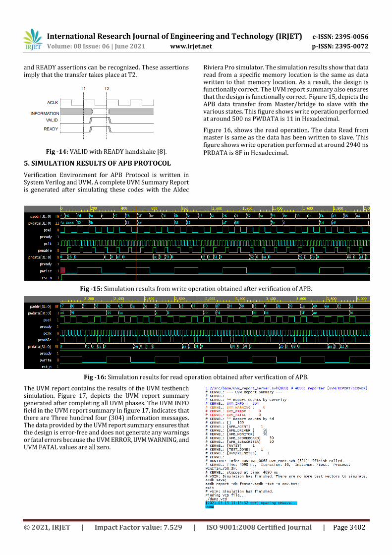
4.3. HANDSHAKE PROCESS IN AXI
To transfer address, data, and control information, all five transaction channels use the same VALID/READY handshake process. This two-way flow control mechanism means that both the master and slave can control the rate at which information is transferred between them. When address, data, or control information is available, the source generates the VALID signal. The READY signal is generated by the destination to indicate that it is ready to accept the information. Only when both the VALID and READY signals are HIGH does transfer occur. There must be no combinatorial paths between input and output signals on master and slave interfaces.
Figures 12–14 depict examples of the handshake process. As shown in Figure 12, the source presents information after T1 and asserts the VALID signal. After T2, the destination asserts the READY signal. The source must maintain the stability of its information until the transfer occurs at T3, when this assertion is recognized.
Fig -12: VALID before READY handshake.
It is not permitted for a source to assert VALID before asserting READY. When VALID is asserted, it must remain asserted until the handshake occurs, which occurs at a rising clock edge when both VALID and READY are asserted.
The destination asserts READY after T1 in Figure 13, before the address, data, or control information is valid. This assertion indicates that it is willing to accept the data. After T2, the source presents the data and asserts VALID, and the transfer occurs at T3, when this assertion is recognized. In this case, transfer takes place in a single cycle.
Fig -13: READY before VALID handshake [8].
It is permissible for a destination to wait for VALID to be asserted before asserting the corresponding READY. If READY is asserted, it is permissible to deassert READY before asserting VALID. Both the source and the destination in Figure 14, indicate that they can transfer the address, data, or control information after T1. In this case, the transfer occurs at the rising clock edge, when both VALID
International Research Journal of Engineering and Technology (IRJET) e-ISSN: 2395-0056
Volume: 08 Issue: 06 | June 2021 www.irjet.net p-ISSN: 2395-0072
© 2021, IRJET | Impact Factor value: 7.529 | ISO 9001:2008 Certified Journal | Page 3402
and READY assertions can be recognized. These assertions imply that the transfer takes place at T2.
Fig -14: VALID with READY handshake [8].
5. SIMULATION RESULTS OF APB PROTOCOL
Verification Environment for APB Protocol is written in System Verilog and UVM. A complete UVM Summary Report is generated after simulating these codes with the Aldec
Riviera Pro simulator. The simulation results show that data read from a specific memory location is the same as data written to that memory location. As a result, the design is functionally correct. The UVM report summary also ensures that the design is functionally correct. Figure 15, depicts the APB data transfer from Master/bridge to slave with the various states. This figure shows write operation performed at around 500 ns PWDATA is 11 in Hexadecimal.
Figure 16, shows the read operation. The data Read from master is same as the data has been written to slave. This figure shows write operation performed at around 2940 ns PRDATA is 8F in Hexadecimal.
Fig -15: Simulation results from write operation obtained after verification of APB.
Fig -16: Simulation results for read operation obtained after verification of APB.
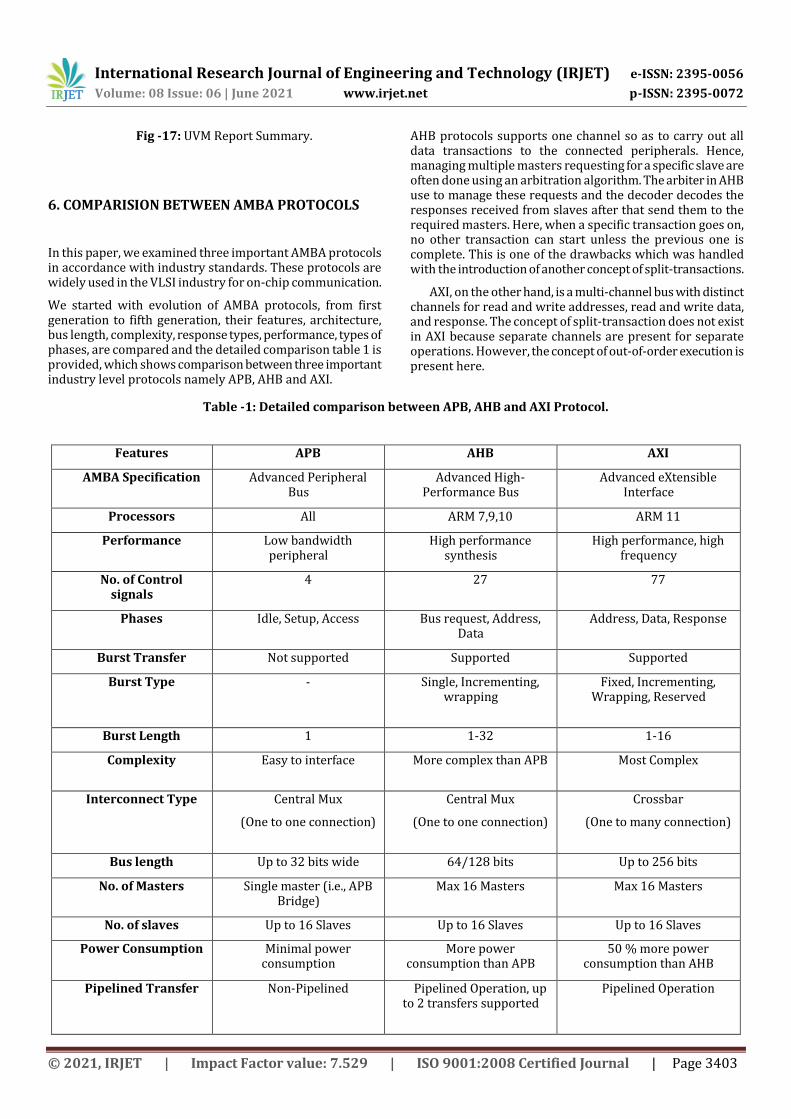
The UVM report contains the results of the UVM testbench simulation. Figure 17, depicts the UVM report summary generated after completing all UVM phases. The UVM INFO field in the UVM report summary in figure 17, indicates that there are Three hundred four (304) information messages. The data provided by the UVM report summary ensures that the design is error-free and does not generate any warnings or fatal errors because the UVM ERROR, UVM WARNING, and UVM FATAL values are all zero.
International Research Journal of Engineering and Technology (IRJET) e-ISSN: 2395-0056
Volume: 08 Issue: 06 | June 2021 www.irjet.net p-ISSN: 2395-0072
© 2021, IRJET | Impact Factor value: 7.529 | ISO 9001:2008 Certified Journal | Page 3403
Fig -17: UVM Report Summary.
6. COMPARISION BETWEEN AMBA PROTOCOLS
In this paper, we examined three important AMBA protocols in accordance with industry standards. These protocols are widely used in the VLSI industry for on-chip communication.
We started with evolution of AMBA protocols, from first generation to fifth generation, their features, architecture, bus length, complexity, response types, performance, types of phases, are compared and the detailed comparison table 1 is provided, which shows comparison between three important industry level protocols namely APB, AHB and AXI.
AHB protocols supports one channel so as to carry out all data transactions to the connected peripherals. Hence, managing multiple masters requesting for a specific slave are often done using an arbitration algorithm. The arbiter in AHB use to manage these requests and the decoder decodes the responses received from slaves after that send them to the required masters. Here, when a specific transaction goes on, no other transaction can start unless the previous one is complete. This is one of the drawbacks which was handled with the introduction of another concept of split-transactions.
AXI, on the other hand, is a multi-channel bus with distinct channels for read and write addresses, read and write data, and response. The concept of split-transaction does not exist in AXI because separate channels are present for separate operations. However, the concept of out-of-order execution is present here.
Table -1: Detailed comparison between APB, AHB and AXI Protocol.
Features APB AHB AXI
AMBA Specification Advanced Peripheral Bus
Advanced High-Performance Bus
Advanced eXtensible Interface
Processors All ARM 7,9,10 ARM 11
Performance Low bandwidth peripheral
High performance synthesis
High performance, high frequency
No. of Control signals
4 27 77
Phases Idle, Setup, Access Bus request, Address, Data
Address, Data, Response
Burst Transfer Not supported Supported Supported
Burst Type - Single, Incrementing, wrapping
Fixed, Incrementing, Wrapping, Reserved
Burst Length 1 1-32 1-16
Complexity Easy to interface More complex than APB Most Complex
Interconnect Type Central Mux
(One to one connection)
Central Mux
(One to one connection)
Crossbar
(One to many connection)
Bus length Up to 32 bits wide 64/128 bits Up to 256 bits
No. of Masters Single master (i.e., APB Bridge)
Max 16 Masters Max 16 Masters
No. of slaves Up to 16 Slaves Up to 16 Slaves Up to 16 Slaves
Power Consumption Minimal power consumption
More power consumption than APB
50 % more power consumption than AHB
Pipelined Transfer Non-Pipelined Pipelined Operation, up to 2 transfers supported
Pipelined Operation
International Research Journal of Engineering and Technology (IRJET) e-ISSN: 2395-0056
Volume: 08 Issue: 06 | June 2021 www.irjet.net p-ISSN: 2395-0072
© 2021, IRJET | Impact Factor value: 7.529 | ISO 9001:2008 Certified Journal | Page 3404
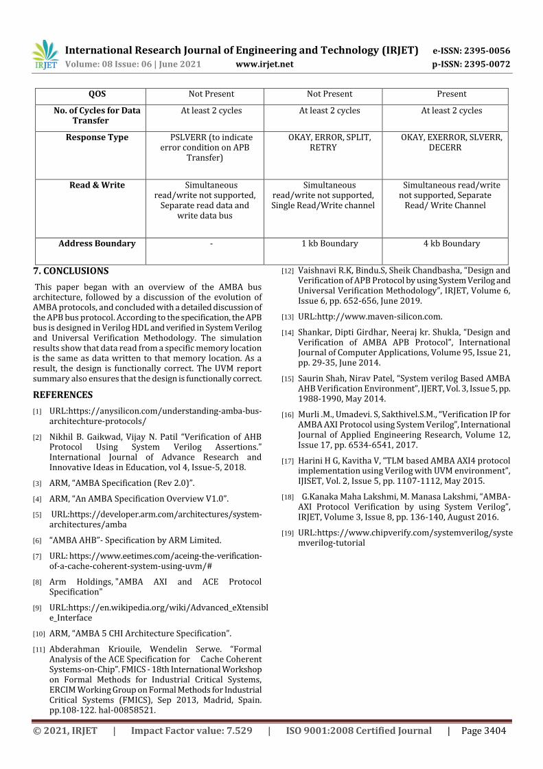
QOS Not Present Not Present Present
No. of Cycles for Data Transfer
At least 2 cycles At least 2 cycles At least 2 cycles
Response Type PSLVERR (to indicate error condition on APB
Transfer)
OKAY, ERROR, SPLIT, RETRY
OKAY, EXERROR, SLVERR, DECERR
Read & Write Simultaneous read/write not supported,
Separate read data and write data bus
Simultaneous read/write not supported, Single Read/Write channel
Simultaneous read/write not supported, Separate
Read/ Write Channel
Address Boundary - 1 kb Boundary 4 kb Boundary
7. CONCLUSIONS
This paper began with an overview of the AMBA bus architecture, followed by a discussion of the evolution of AMBA protocols, and concluded with a detailed discussion of the APB bus protocol. According to the specification, the APB bus is designed in Verilog HDL and verified in System Verilog and Universal Verification Methodology. The simulation results show that data read from a specific memory location is the same as data written to that memory location. As a result, the design is functionally correct. The UVM report summary also ensures that the design is functionally correct.
REFERENCES
[1] URL:https://anysilicon.com/understanding-amba-bus-architechture-protocols/
[2] Nikhil B. Gaikwad, Vijay N. Patil “Verification of AHB Protocol Using System Verilog Assertions.” International Journal of Advance Research and Innovative Ideas in Education, vol 4, Issue-5, 2018.
[3] ARM, “AMBA Specification (Rev 2.0)”.
[4] ARM, “An AMBA Specification Overview V1.0”.
[5] URL:https://developer.arm.com/architectures/system-architectures/amba
[6] “AMBA AHB”- Specification by ARM Limited.
[7] URL: https://www.eetimes.com/aceing-the-verification-of-a-cache-coherent-system-using-uvm/#
[8] Arm Holdings, "AMBA AXI and ACE Protocol Specification"
[9] URL:https://en.wikipedia.org/wiki/Advanced_eXtensible_Interface
[10] ARM, “AMBA 5 CHI Architecture Specification”.
[11] Abderahman Kriouile, Wendelin Serwe. “Formal Analysis of the ACE Specification for Cache Coherent Systems-on-Chip”. FMICS - 18th International Workshop on Formal Methods for Industrial Critical Systems, ERCIM Working Group on Formal Methods for Industrial Critical Systems (FMICS), Sep 2013, Madrid, Spain. pp.108-122. hal-00858521.
[12] Vaishnavi R.K, Bindu.S, Sheik Chandbasha, “Design and Verification of APB Protocol by using System Verilog and Universal Verification Methodology”, IRJET, Volume 6, Issue 6, pp. 652-656, June 2019.
[13] URL:http://www.maven-silicon.com.
[14] Shankar, Dipti Girdhar, Neeraj kr. Shukla, “Design and Verification of AMBA APB Protocol”, International Journal of Computer Applications, Volume 95, Issue 21, pp. 29-35, June 2014.
[15] Saurin Shah, Nirav Patel, “System verilog Based AMBA AHB Verification Environment”, IJERT, Vol. 3, Issue 5, pp. 1988-1990, May 2014.
[16] Murli .M., Umadevi. S, Sakthivel.S.M., “Verification IP for AMBA AXI Protocol using System Verilog”, International Journal of Applied Engineering Research, Volume 12, Issue 17, pp. 6534-6541, 2017.
[17] Harini H G, Kavitha V, “TLM based AMBA AXI4 protocol implementation using Verilog with UVM environment”, IJISET, Vol. 2, Issue 5, pp. 1107-1112, May 2015.
[18] G.Kanaka Maha Lakshmi, M. Manasa Lakshmi, “AMBA-AXI Protocol Verification by using System Verilog”, IRJET, Volume 3, Issue 8, pp. 136-140, August 2016.
[19] URL:https://www.chipverify.com/systemverilog/systemverilog-tutorial