comparison of a state of the art si igbt and next ... · table i. since sic switching devices are...
TRANSCRIPT
General rights Copyright and moral rights for the publications made accessible in the public portal are retained by the authors and/or other copyright owners and it is a condition of accessing publications that users recognise and abide by the legal requirements associated with these rights.
Users may download and print one copy of any publication from the public portal for the purpose of private study or research.
You may not further distribute the material or use it for any profit-making activity or commercial gain
You may freely distribute the URL identifying the publication in the public portal If you believe that this document breaches copyright please contact us providing details, and we will remove access to the work immediately and investigate your claim.
Downloaded from orbit.dtu.dk on: Mar 11, 2020
Comparison of a state of the art Si IGBT and next generation fast switching devices ina 4 kW boost converter
Anthon, Alexander; Zhang, Zhe; Andersen, Michael A. E.
Published in:Proceedings of 2015 IEEE Energy Conversion Congress and Exposition
Link to article, DOI:10.1109/ECCE.2015.7310080
Publication date:2015
Document VersionPeer reviewed version
Link back to DTU Orbit
Citation (APA):Anthon, A., Zhang, Z., & Andersen, M. A. E. (2015). Comparison of a state of the art Si IGBT and nextgeneration fast switching devices in a 4 kW boost converter. In Proceedings of 2015 IEEE Energy ConversionCongress and Exposition (pp. 3003-3011). IEEE. https://doi.org/10.1109/ECCE.2015.7310080

Comparison of a State of the Art Si IGBT and NextGeneration Fast Switching Devices in a 4 kW Boost
ConverterAlexander Anthon, Zhe Zhang, Michael A. E. Andersen
Dept. of Electrical EngineeringTechnical University of Denmark
Kgs. Lyngby, DenmarkEmail: [email protected]
Abstract—This paper gives a comprehensive comparison oftwo promising silicon carbide (SiC) switching devices, i.e.normally-off SiC MOSFET and a normally-on SiC JFET, asalternatives to a conventional state of the art Si IGBT. Thecomparison uses datasheet information to determine conductionlosses, switching transition measurements for switching losscalculations and electrical power measurements in a boostconverter. Using SiC switching devices, switching energies canbe reduced by almost 70 % and the forward voltages of suchdevices are much lower compared to the IGBT which then reducethe conduction losses. This reduction in semiconductor lossescan increase overall converter efficiencies up to 0.4 % at 20 kHzor enable high frequency operation up to 100 kHz which thenreduces the size and weight of the inductor by more than 75 %while still achieving efficiencies over 98.3 %.
Index Terms—Si IGBT, SiC MOSFET, SiC JFET, Efficiency,Boost converter
I. INTRODUCTION
In residential photovoltaic (PV) systems, transformer-lesstopologies are favored due to the smaller size, weight,lower cost and higher efficiencies compared to theirtransformer-based alternatives [1]. However, a boost converteras a preregulator is then necessary in order to ensure a DClink voltage large enough to obtain the desired grid voltage.For three-phase PV systems, the DC link voltage is typicallyin the range of 700 V and can reach up to 1000 V. Thus,the semiconductor devices are typically chosen to have abreakdown voltage of 1200 V, which limits the choice mainlyto Si IGBTs.
For power converters equipped with such semiconductordevices, however, the switching frequency usually becomesthe limiting factor when it comes to high efficiency powerconversion. Where a simple boost converter generally requiresonly one diode, one switching element and one inductor, thelatter in this configuration usually becomes bulky, heavy andexpensive due to the low switching frequency operation ofthe Si IGBT in order to maintain a reasonable small inputcurrent ripple. Interleaved boost converter (IBC) topologiescan therefore be an attractive alternative due to the reducedinput current ripple [2] which consequently improves thepower quality and power-point tracking (MPPT) performance
[3] with the trade-offs against other criteria such as additionalcomponents, increased complexity or unequal load sharing [4].To furthermore improve the performance of the preregulatorstage of the PV system, previous work has investigated theuse of new semiconductor devices made of silicon carbide(SiC) material. With the commercialization of SiC diodes in2001 [5], which have the particular benefit of having zeroreverse recovery current, the positive impact of the new kindof semiconductor devices on switching loss reduction andreduced electromagnetic interference (EMI) has been reportedfor instance in [6], [7] and efficiency improvements of up to0.8 % in a boost converter with SiC diodes were achieved in[3].
After the successful commercialization of SiC diodes,research interest has moved towards the utilization of SiCsemiconductor switching devices in power converters as directreplacements for Si IGBTs and Si MOSFETs. Due to thehigher electric field breakdown strength of SiC material, notonly the on-resistance can be reduced compared to a SiMOSFET of an equivalent rating [8], but also the switchingenergies (in particular compared to IGBTs [9]). The benefitsof SiC switching devices compared to Si based alternativesfor various applications have been reported in previous work[10]–[15].
Among the various SiC switching alternatives to date,two main candidates can be pointed out and are henceintensively tested in this work: The normally-off SiC MOSFETand the normally-on SiC JFET. Although previous workclearly highlights the potentials of these two SiC switchingdevices, neither of them have fully become the new standardcomponent in commercial products. Apart from the smallavailability through distribution channels, main issues arerelated to the (long-term) reliability, which is still ongoingresearch work [16]–[18].
The SiC MOSFET is claimed to have long-term reliabilityissues due to its thin oxide layer [19], [20], which is a majorreason for not utilizing it in commercial products. In contrast,the depletion mode JFET does not have the reliability issue likethe SiC MOSFET and shows a superior short circuit behavior[21], however its normally-on behavior is the main argument
978-1-4673-7151-3/15/$31.00 c©2015 IEEE
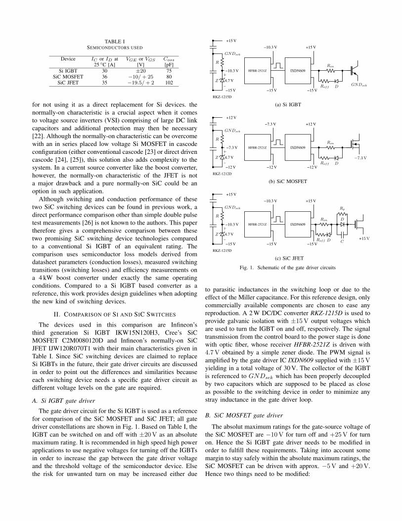
TABLE ISEMICONDUCTORS USED
Device IC or ID at VGE or VGS Coss
25 C [A] [V] [pF]Si IGBT 30 ±20 75
SiC MOSFET 36 −10/ + 25 80SiC JFET 35 −19.5/ + 2 102
for not using it as a direct replacement for Si devices. thenormally-on characteristic is a crucial aspect when it comesto voltage source inverters (VSI) comprising of large DC linkcapacitors and additional protection may then be necessary[22]. Although the normally-on characteristic can be overcomewith an in series placed low voltage Si MOSFET in cascodeconfiguration (either conventional cascode [23] or direct drivencascode [24], [25]), this solution also adds complexity to thesystem. In a current source converter like the boost converter,however, the normally-on characteristic of the JFET is nota major drawback and a pure normally-on SiC could be anoption in such application.
Although switching and conduction performance of thesetwo SiC switching devices can be found in previous work, adirect performance comparison other than simple double pulsetest measurements [26] is not known to the authors. This papertherefore gives a comprehensive comparison between thesetwo promising SiC switching device technologies comparedto a conventional Si IGBT of an equivalent rating. Thecomparison uses semiconductor loss models derived fromdatasheet parameters (conduction losses), measured switchingtransitions (switching losses) and efficiency measurements ona 4 kW boost converter under exactly the same operatingconditions. Compared to a Si IGBT based converter as areference, this work provides design guidelines when adoptingthe new kind of switching devices.
II. COMPARISON OF SI AND SIC SWITCHES
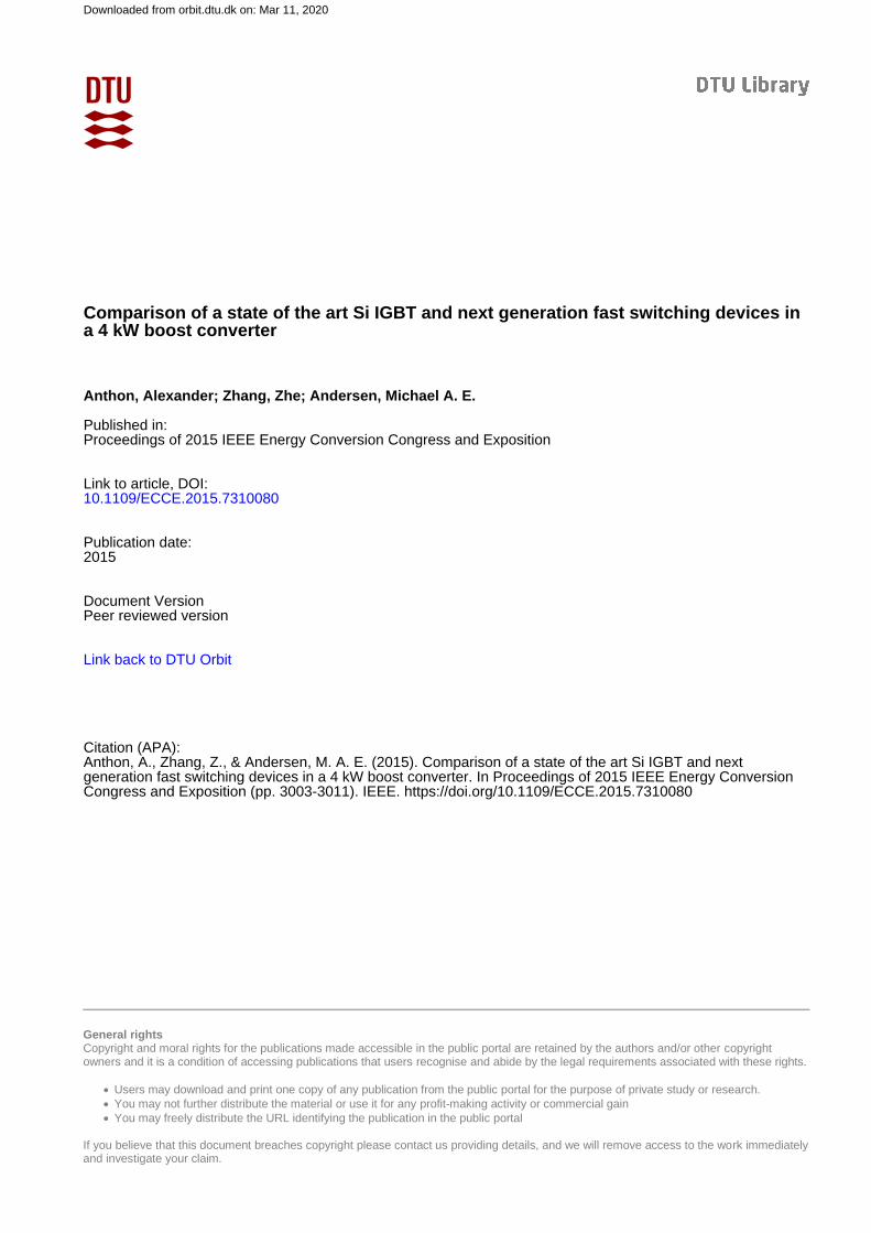
The devices used in this comparison are Infineon’sthird generation Si IGBT IKW15N120H3, Cree’s SiCMOSFET C2M0080120D and Infineon’s normally-on SiCJFET IJW120R070T1 with their main characteristics given inTable I. Since SiC switching devices are claimed to replaceSi IGBTs in the future, their gate driver circuits are discussedin order to point out the differences and similarities becauseeach switching device needs a specific gate driver circuit asdifferent voltage levels on the gate are required.
A. Si IGBT gate driver
The gate driver circuit for the Si IGBT is used as a referencefor comparison of the SiC MOSFET and SiC JFET; all gatedriver constellations are shown in Fig. 1. Based on Table I, theIGBT can be switched on and off with ±20 V as an absolutemaximum rating. It is recommended in high speed high powerapplications to use negative voltages for turning off the IGBTsin order to increase the gap between the gate driver voltageand the threshold voltage of the semiconductor device. Elsethe risk for unwanted turn on may be increased either due
RKZ-1215D
−15 V
Z−
+
4.7 V
R
−10.3 V
GNDsek
+15 V
−15 V
−10.3 V
HFBR-2521Z
+15 V
−15 V
IXDN609Ron
DRoffGNDsek
(a) Si IGBT
RKZ-1212D
−12 V
Z−
+
4.7 V
R
−7.3 V
GNDsek
+12 V
−12 V
−7.3 V
HFBR-2521Z
+12 V
−12 V
IXDN609Ron
DRoff
−7.3V
(b) SiC MOSFET
RKZ-1215D
−15 V
Z−
+
4.7 V
R
−10.3 V
GNDsek
+15 V
−15 V
−10.3 V
HFBR-2521Z
+15 V
−15 V
IXDN609Ron
DRoff
D
Rp
C+15V
(c) SiC JFET
Fig. 1. Schematic of the gate driver circuits
to parasitic inductances in the switching loop or due to theeffect of the Miller capacitance. For this reference design, onlycommercially available components are chosen to ease anyreproduction. A 2 W DC/DC converter RKZ-1215D is used toprovide galvanic isolation with ±15 V output voltages whichare used to turn the IGBT on and off, respectively. The signaltransmission from the control board to the power stage is donewith optic fiber, whose receiver HFBR-2521Z is driven with4.7 V obtained by a simple zener diode. The PWM signal isamplified by the gate driver IC IXDN609 supplied with ±15 Vyielding in a total voltage of 30 V. The collector of the IGBTis referenced to GNDsek which has been properly decoupledby two capacitors which are supposed to be placed as closeas possible to the switching device in order to minimize anystray inductance in the gate driver loop.
B. SiC MOSFET gate driver
The absolut maximum ratings for the gate-source voltage ofthe SiC MOSFET are −10 V for turn off and +25 V for turnon. Hence the Si IGBT gate driver needs to be modified inorder to fulfill these requirements. Taking into account somemargin to stay safely within the absolute maximum ratings, theSiC MOSFET can be driven with approx. −5 V and +20 V.Hence two things need to be modified:
1) Replace the DC/DC converter with the RKZ-1212Dwhich provides galvanic isolation and two outputvoltages ±12 V
2) Reference the source of the SiC MOSFET to the voltageof the zener diode, i.e. −7.3 V
The driving voltage for turn on is then according to Kirchoff’svoltage law (KVL)
VGSon = +12 V − (−7.3 V) = 19.3 V (1)
and the turn off voltage, respectively
VGSoff = −12 V − (−7.3 V) = −4.7 V (2)
Hence the SiC MOSFET can easily be adapted into a Si IGBTbased converter with only minor modifications. Basically, onlya change in the DC/DC converter and the reference voltage arenecessary.
C. SiC JFET gate driverThe gate driver circuit for the SiC JFET requires more
attention since the device differs internally from IGBTs orMOSFETs [27]. Since the JFET is a depletion mode device,it is turned on with a control voltage of 0 V and a negativevoltage must be applied to turn the device off. The datasheetstates this pinch-off voltage of the JFET to be around −16 Vwhich may vary from one device to another. Furthermore,at around −23 V, the gate-source junction enters reversebreakdown and hence a gate-source voltage of −20 V isusually recommended in order to fully turn the device off.In [27], a driver circuit for a normally-on JFET is proposed toovercome this particular issue with the reverse breakdown, andit is therefore used in this work. Where the detailed explanationof the gate driver can be found in [27], it is only mentionedhere that three additional electronic components are neededand the reference voltage, once again, must be shifted. Thetwo modifications for the SiC JFET gate driver are therefore:
1) Place a RCD network between the gate resistance andthe gate of the JFET
2) Reference the source of the JFET to the positive supplyvoltage of the DC/DC converter output, i.e. +15 V
D. Static characteristicsOne of the properties of SiC based switching devices
is to reduce the conduction losses. The voltage drop ofa semiconductor device directly relates to the conductionlosses which represent a significant contribution to the overallconverter losses. The specific forward voltages for the devicesused in this work are taken from datasheet information andare presented in Fig. 2. Once can see that over the wholecurrent range of interest, the Si IGBT has the largest forwardvoltages. The reason for that is that the IGBT is a bipolarswitching device which can be modeled as a series connectionof a voltage source representing the zero on-state voltage V0
and a dynamic resistance ron. For a unipolar device suchas the SiC MOSFET and the SiC JFET, there is no zeroon-state voltage and only the channel resistance Ron is given.Hence, conduction losses of both SiC switching devices willbe smaller at any given operating point in this work.
Current [A]
0 2 4 6 8 10 12
Volt
age
[V]
0
0.5
1
1.5
2
2.5
3
SiC JFET
SiC MOSFET
Si IGBT
Fig. 2. Forward voltages of different switching devices at 25 C junctiontemperature
E. Dynamic characteristics
Another benefit when using SiC devices are the reducedswitching losses in a given converter application. In an initialdesign approach, switching energies are mostly comparedbased on the information provided in the datasheet. However,this may lead to unfair comparisons if the test setup differ fromone manufacturer to another (use of different free-wheelingdiodes with different reverse recovery currents, different gateresistors, etc.). Therefore, this work compares the switchingenergies at exactly the same test conditions including the sameinductor and the same free-wheeling diode. Furthermore, thegate resistors are adjusted to maintain a similar peak gatecurrent for a fair comparison. The test setup is shown in Fig. 3aand the current measurement (flat current shunt) is shown inFig. 3b which has been presented in [28].
The gate-source/gate-emitter voltages are measured with aLeCroy PP011 voltage probe having a bandwidth of 500 MHz,the drain-source/collector-emitter voltages are measured witha 400 MHz LeCroy PPE4kV voltage probe. The voltagedrop across the shunt resistor is measured with a LeCroyPP011 voltage probe as well which is then translated backto the current according to Ohm’s law. The turn on switchingtransitions of all three devices are shown in Fig. 4. One canclearly see the superior switching performance of the two SiCswitching devices compared to the Si IGBT. All waveformsare captured such that the gate turn on occurs at the same time.The SiC MOSFET and the SiC JFET show similar switchingspeeds. Where the SiC MOSFET has a lower di/dt comparedto the SiC JFET, its dv/dt is higher. Hence similar turn onswitching energies are expected for the MOSFET and theJFET.
The turn off switching transitions are shown in Fig. 5 inorder to complete the dynamic performance comparison. Alsoduring the turn off events, both SiC switching devices showmuch faster transitions than the IGBT. However, within thecomparison of SiC devices, the MOSFET turns off quickerthan the SiC JFET alternative. Maximum dv/dt and di/dt valuesfor each switching device are shown in Table II in orderto quantify the switching transitions. Having the voltage and

(a) Double pulse test setup
(b) Current measurement
Fig. 3. Double pulse test setup and current measurement
current measured on the oscilloscope, switching energies canthen be obtained by numerically integrating the instantaneouspower (which is simply the product of the measured voltageand current). The results of this procedure for currents from2 A to 10 A are shown in Fig. 6. It verifies that the Si IGBT hashighest switching energies for both turn on and turn off, thoughthe discrepancy is larger at the turn off energies. That is mainlydue to the tail current associated to Si IGBTs. Especiallyat larger currents, the SiC devices outperform the Si IGBT.Comparing the SiC switching devices, the SiC MOSFETshows lower turn off switching energies compared to its SiCJFET competitor at increased currents.
III. BOOST CONVERTER
Based on the previous analysis, the performance comparisonbetween the SiC switching devices can be extended to a lossanalysis for a given power converter; in this work it is a boostconverter with specifications for a typical PV system whoseblock diagram is shown in Fig. 7a. The main components ofthe boost converter are the boost inductor L, the switchingelement S and a diode D as depicted in Fig. 7b. Assumingcontinuous conduction mode (CCM) with two different inputvoltages, 400 V and 500 V, and a fixed output voltage of 700 V,the duty cycle d can then be calculated according to
d = 1 − Vin
Vout(3)
TABLE IISWITCHING EVALUATION
Turn on Turn off
IGBT MOSFET JFET IGBT MOSFET JFET
dv/dt in kV/µs 16 40 23 8 27 18di/dt in kA/µs 0.5 1.1 3.3 0.06 0.3 0.2
(a) Turn on IGBT, Rg = 18 Ω
(b) Turn on MOSFET, Rg = 18 Ω
(c) Turn on JFET, Rg = 10 Ω
Fig. 4. Turn on transitions. VDC = 800 V, I = 10 A
Maximum output power is set to 4 kW in this work to representa residential PV system. The DC component of the currentflowing through the boost inductor can then be calculated
ILDC =
VinPout
(1 − d)2V 2out
(4)
The current ripple is often a crucial factor when designingthe boost converter as it creates harmonics and causes EMI. Atypical design procedure is to limit the current ripple ∆I to bearound 20 % of the DC current. With a switching frequencyfsw initially set to 20 kHz in order to avoid audible noisecoming from the inductor, the size of the inductor is calculatedto be 3 mH.
L =Vind
2∆Ifsw(5)
This yields in a current ripple of 22 %. The 3 mH boostinductor is taken from a commercial PV inverter and it

(a) Turn off IGBT, Rg = 18 Ω
(b) Turn off MOSFET, Rg = 18 Ω
(c) Turn off JFET, Rg = 10 Ω
Fig. 5. Turn off transitions. VDC = 800 V, I = 10 A
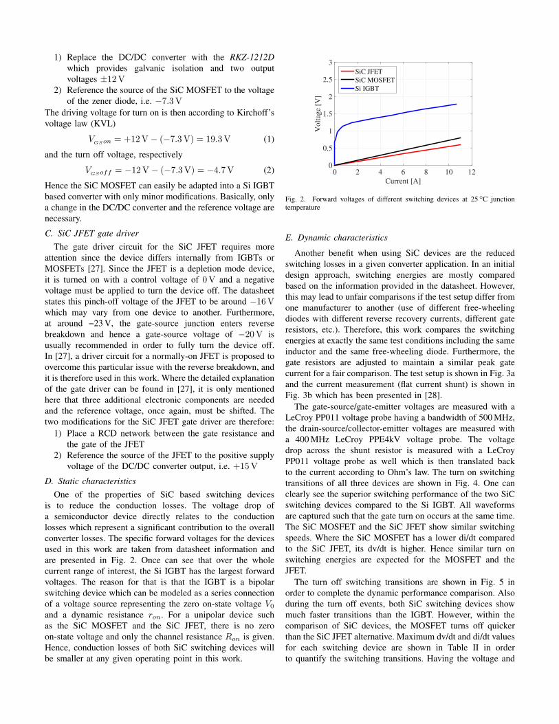
comprises of six KoolMu 77439-A7 cores stacked togetherwith 60 turns. Taking advantage of the superior switchingcharacteristics of the SiC switching devices, the switchingfrequency is increased to 100 kHz in this work which thenreduces the size of the inductor for a given current rippleaccording to Eq. (5). The new inductor is set to 1 mH whichwill result in a current ripple percentage of 13 % only. Thisgives a current ripple decrease of more than 40 %. The newinductor is made of one MPP 55192-A2 core which in generalmay be more expensive than KoolMu, but it has a superiorcore loss performance which is very attractive at increasedswitching frequency operation. Also, due to the reductionin inductor size, only one core is necessary whereas the3 mH core uses six KoolMu cores stacked together. Table IIIsummarizes the most important specifications and Fig. 8 showsboth inductors used in this work.
Current [A]
2 4 6 8 10
Ener
gy [µ
J]
0
100
200
300
400
500
SiC JFET
SiC MOSFET
Si IGBT
(a) Turn on energies
Current [A]
2 4 6 8 10
Ener
gy [µ
J]0
100
200
300
400
500
SiC JFET
SiC MOSFET
Si IGBT
(b) Turn off energies
Fig. 6. Switching energy comparison of the three devices for different currentlevels. VDC = 800 V
EMI
Inputfilter
PV panel DC/DCconverter
DC/ACinverter
Outputfilter
Grid
(a) Block diagram of a PV inverter system
Cin
L D
CoutVin VoutS
(b) Boost converter
Fig. 7. Block diagram of PV system in (a), schematic of a single phase boostconverter in (b)
TABLE IIIBOOST INDUCTOR PARAMETERS
Inductor 1 Inductor 2Inductance in [mH] 3 1
Cores 6xKoolMu 77439-A7 1xMPP 55192-A2Turns 60 88
Volume in [cm3] 345 72Weight in [g] 1000 230
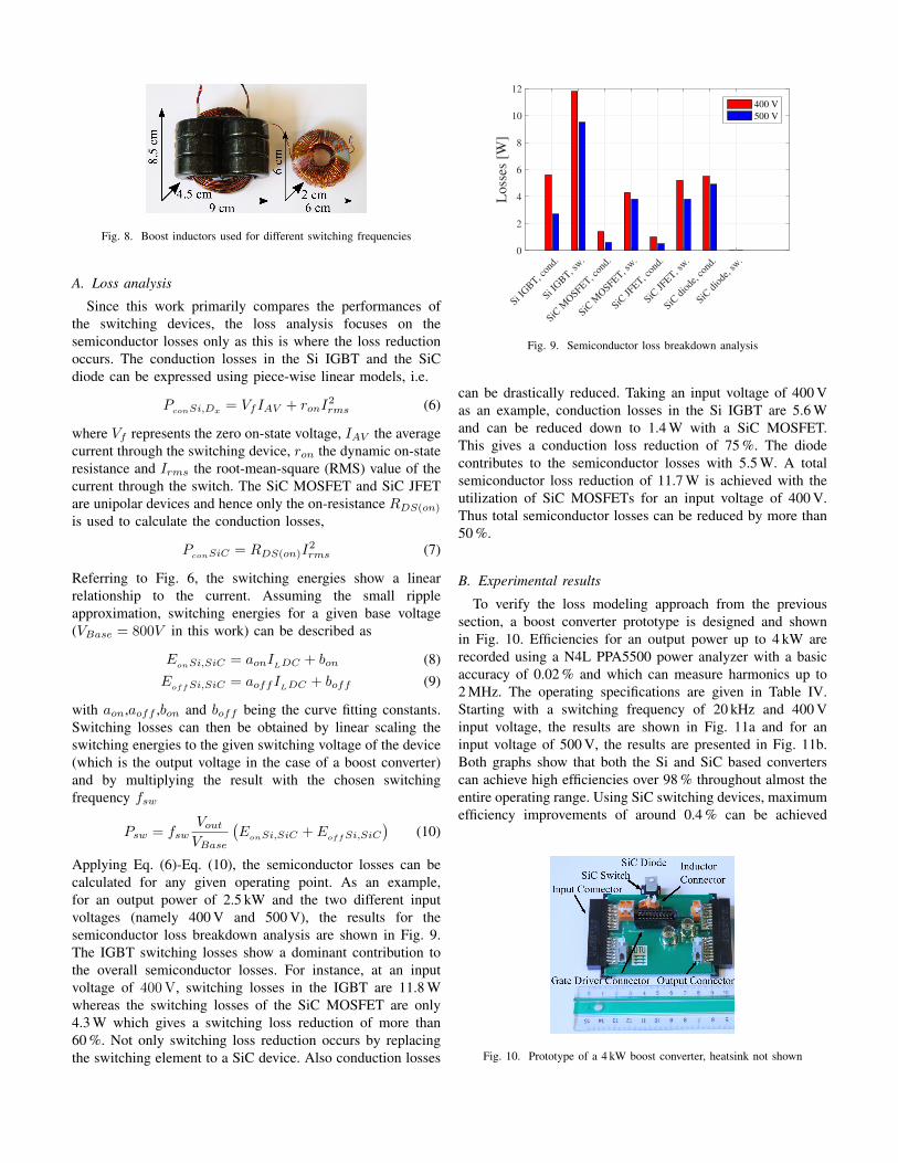
Fig. 8. Boost inductors used for different switching frequencies
A. Loss analysis
Since this work primarily compares the performances ofthe switching devices, the loss analysis focuses on thesemiconductor losses only as this is where the loss reductionoccurs. The conduction losses in the Si IGBT and the SiCdiode can be expressed using piece-wise linear models, i.e.
PconSi,Dx = VfIAV + ronI2rms (6)
where Vf represents the zero on-state voltage, IAV the averagecurrent through the switching device, ron the dynamic on-stateresistance and Irms the root-mean-square (RMS) value of thecurrent through the switch. The SiC MOSFET and SiC JFETare unipolar devices and hence only the on-resistance RDS(on)
is used to calculate the conduction losses,
PconSiC = RDS(on)I2rms (7)
Referring to Fig. 6, the switching energies show a linearrelationship to the current. Assuming the small rippleapproximation, switching energies for a given base voltage(VBase = 800V in this work) can be described as
EonSi,SiC = aonILDC + bon (8)
EoffSi,SiC = aoffILDC + boff (9)
with aon,aoff ,bon and boff being the curve fitting constants.Switching losses can then be obtained by linear scaling theswitching energies to the given switching voltage of the device(which is the output voltage in the case of a boost converter)and by multiplying the result with the chosen switchingfrequency fsw
Psw = fswVout
VBase
(EonSi,SiC + E
offSi,SiC
)(10)
Applying Eq. (6)-Eq. (10), the semiconductor losses can becalculated for any given operating point. As an example,for an output power of 2.5 kW and the two different inputvoltages (namely 400 V and 500 V), the results for thesemiconductor loss breakdown analysis are shown in Fig. 9.The IGBT switching losses show a dominant contribution tothe overall semiconductor losses. For instance, at an inputvoltage of 400 V, switching losses in the IGBT are 11.8 Wwhereas the switching losses of the SiC MOSFET are only4.3 W which gives a switching loss reduction of more than60 %. Not only switching loss reduction occurs by replacingthe switching element to a SiC device. Also conduction losses
Si IG
BT, c
ond.
Si IG
BT, s
w.
SiC M
OSFE
T, c
ond.
SiC M
OSFE
T, s
w.
SiC JFE
T, c
ond.
SiC JFE
T, s
w.
SiC d
iode
, con
d.
SiC d
iode
, sw
.
Loss
es
[W]
0
2
4
6
8
10
12
400 V
500 V
Fig. 9. Semiconductor loss breakdown analysis
can be drastically reduced. Taking an input voltage of 400 Vas an example, conduction losses in the Si IGBT are 5.6 Wand can be reduced down to 1.4 W with a SiC MOSFET.This gives a conduction loss reduction of 75 %. The diodecontributes to the semiconductor losses with 5.5 W. A totalsemiconductor loss reduction of 11.7 W is achieved with theutilization of SiC MOSFETs for an input voltage of 400 V.Thus total semiconductor losses can be reduced by more than50 %.
B. Experimental results
To verify the loss modeling approach from the previoussection, a boost converter prototype is designed and shownin Fig. 10. Efficiencies for an output power up to 4 kW arerecorded using a N4L PPA5500 power analyzer with a basicaccuracy of 0.02 % and which can measure harmonics up to2 MHz. The operating specifications are given in Table IV.Starting with a switching frequency of 20 kHz and 400 Vinput voltage, the results are shown in Fig. 11a and for aninput voltage of 500 V, the results are presented in Fig. 11b.Both graphs show that both the Si and SiC based converterscan achieve high efficiencies over 98 % throughout almost theentire operating range. Using SiC switching devices, maximumefficiency improvements of around 0.4 % can be achieved
Fig. 10. Prototype of a 4 kW boost converter, heatsink not shown
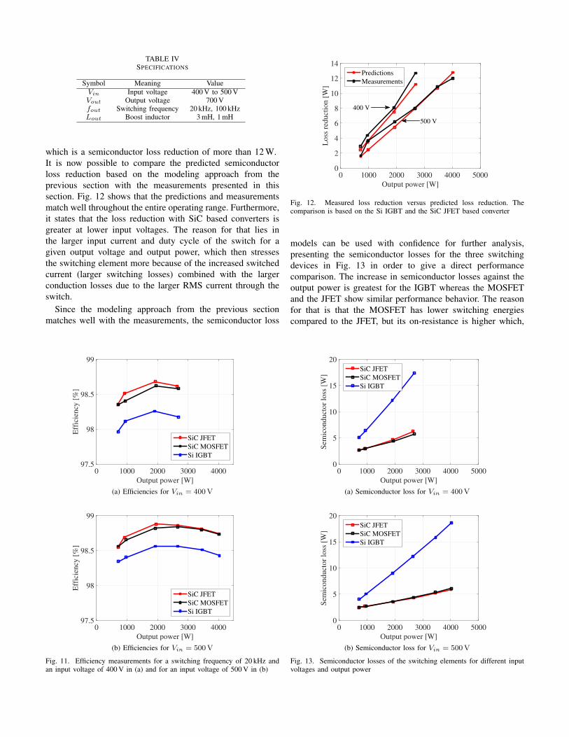
TABLE IVSPECIFICATIONS
Symbol Meaning ValueVin Input voltage 400 V to 500 VVout Output voltage 700 Vfout Switching frequency 20 kHz, 100 kHzLout Boost inductor 3 mH, 1 mH
which is a semiconductor loss reduction of more than 12 W.It is now possible to compare the predicted semiconductorloss reduction based on the modeling approach from theprevious section with the measurements presented in thissection. Fig. 12 shows that the predictions and measurementsmatch well throughout the entire operating range. Furthermore,it states that the loss reduction with SiC based converters isgreater at lower input voltages. The reason for that lies inthe larger input current and duty cycle of the switch for agiven output voltage and output power, which then stressesthe switching element more because of the increased switchedcurrent (larger switching losses) combined with the largerconduction losses due to the larger RMS current through theswitch.
Since the modeling approach from the previous sectionmatches well with the measurements, the semiconductor loss
Output power [W]
0 1000 2000 3000 4000
Eff
icie
ncy
[%
]
97.5
98
98.5
99
SiC JFET
SiC MOSFET
Si IGBT
(a) Efficiencies for Vin = 400 V
Output power [W]
0 1000 2000 3000 4000
Eff
icie
ncy
[%
]
97.5
98
98.5
99
SiC JFET
SiC MOSFET
Si IGBT
(b) Efficiencies for Vin = 500 V
Fig. 11. Efficiency measurements for a switching frequency of 20 kHz andan input voltage of 400 V in (a) and for an input voltage of 500 V in (b)
Output power [W]
0 1000 2000 3000 4000 5000
Loss
red
uct
ion [
W]
0
2
4
6
8
10
12
14
400 V
500 V
Predictions
Measurements
Fig. 12. Measured loss reduction versus predicted loss reduction. Thecomparison is based on the Si IGBT and the SiC JFET based converter
models can be used with confidence for further analysis,presenting the semiconductor losses for the three switchingdevices in Fig. 13 in order to give a direct performancecomparison. The increase in semiconductor losses against theoutput power is greatest for the IGBT whereas the MOSFETand the JFET show similar performance behavior. The reasonfor that is that the MOSFET has lower switching energiescompared to the JFET, but its on-resistance is higher which,
Output power [W]
0 1000 2000 3000 4000 5000
Sem
iconduct
or
loss
[W
]
0
5
10
15
20
SiC JFET
SiC MOSFET
Si IGBT
(a) Semiconductor loss for Vin = 400 V
Output power [W]
0 1000 2000 3000 4000 5000
Sem
iconduct
or
loss
[W
]
0
5
10
15
20
SiC JFET
SiC MOSFET
Si IGBT
(b) Semiconductor loss for Vin = 500 V
Fig. 13. Semiconductor losses of the switching elements for different inputvoltages and output power

Output power [W]
0 1000 2000 3000 4000
Eff
icie
ncy
[%
]
96
96.5
97
97.5
98
98.5
99
SiC JFET
SiC MOSFET
(a) Efficiencies for Vin = 400 V
Output power [W]
0 1000 2000 3000 4000
Eff
icie
ncy
[%
]
96
96.5
97
97.5
98
98.5
99
SiC JFET
SiC MOSFET
(b) Efficiencies for Vin = 500 V
Fig. 14. Efficiency measurements for a switching frequency of 100 kHz andan input voltage of 400 V in (a) and for an input voltage of 500 V in (b)
in the end, results in very similar total semiconductor lossesthroughout the entire operating range.
Using SiC switching devices for increased switchingfrequency operation, in order to reduce the size of the passivecomponents measurements are repeated for 100 kHz operationwith the 1 mH inductor. The results are shown in Fig. 14.Also at higher switching frequencies, efficiencies are still closeto each other and a peak value of up to 98.3 % is achieved.Only at low power operation, a significant drop in efficiencyis present mainly because the switching losses and the corelosses are major contributions in that operating range. It isworthy of comment that the SiC JFET seems to have higherefficiencies especially in the lower power range. Referring toFig. 6, the SiC JFET has quite competitive turn off switchingenergies to the SiC MOSFET at low currents and the differencebecomes only significant as the current increases. However,as the current increases at increased output power, the JFETcan benefit from its lower on-resistance. Therefore, insteadof looking at the overall efficiencies, semiconductor lossesare used (based on the modeling approach from the previoussection), shown in Fig. 15. One can see that the semiconductorlosses of the SiC MOSFET become slightly lower comparedto the JFET - especially at increased power levels. Thatis due to the superior turn off energies of the MOSFETwhich outperform the lower conduction losses of the JFET
Output power [W]
0 1000 2000 3000 4000 5000
Sem
iconduct
or
loss
[W
]
0
10
20
30
40
SiC JFET
SiC MOSFET
(a) Semiconductor loss for Vin = 400 V
Output power [W]
0 1000 2000 3000 4000 5000S
emic
onduct
or
loss
[W
]0
10
20
30
40
SiC JFET
SiC MOSFET
(b) Semiconductor loss for Vin = 500 V
Fig. 15. Semiconductor losses of the switching elements for different inputvoltages and output power
at this particular switching frequency. From a semiconductorloss point of view, the SiC MOSFET has total losses ofalmost 22 W at 400 V input voltage whereas the JFET hasaround 26 W. However, such loss reduction of 4 W operatingat 2.6 kW output power has only a minor influence on theoverall efficiency. The same statement can be extended to theoperation with 500 V input voltage and up to 4 kW outputpower. Hence for the given specifications in this work, boththe JFET and the MOSFET perform very similar in terms ofsemiconductor losses.
IV. CONCLUSION
In this paper, three state of the art switching devices havebeen compared to each other. The comparison uses analyticalsemiconductor loss models based on conduction losses derivedfrom datasheet information, and switching losses obtainedvia switching transition measurements. The loss models andhence the predicted semiconductor loss reduction with the useof SiC switching devices are verified using electrical powermeasurements in a boost converter operating under variousconditions up to 4 kW. Both SiC based converters achievehigh efficiencies of up to 98.8 % at a switching frequencyof 20 kHz, which is 0.4 % higher than its Si alternative.At that operating frequency, both SiC alternatives performvery similar. With SiC switching devices utilized, operating

frequency is increased up to 100 kHz which reduces theboost inductance from 3 mH down to 1 mH. This not onlyreduces the current ripple from 22 % down to 13 %, but alsoreduces the size and weight of the inductor by over 75 %.Even at 100 kHz operation, competitive efficiencies of up to98.3 % can be achieved and both SiC alternatives show similarsemiconductor losses. Therefore, within the specifications inthis work, one SiC switching device can not be favored overthe other based on a loss point of view.
REFERENCES
[1] T. Kerekes, R. Teodorescu, P. Rodrıguez, G. Vazquez, and E. Aldabas,“A new high-efficiency single-phase transformerless PV invertertopology,” IEEE Trans. Ind. Electron., vol. 58, no. 1, pp. 184–191, Jan2011.
[2] D.-Y. Jung, Y.-H. Ji, S.-H. Park, Y.-C. Jung, and C.-Y. Won, “Interleavedsoft-switching boost converter for photovoltaic power-generationsystem,” IEEE Trans. Power Electron., vol. 26, no. 4, pp. 1137–1145,April 2011.
[3] C.-M. Ho, H. Breuninger, S. Pettersson, G. Escobar, and F. Canales, “Acomparative performance study of an interleaved boost converter usingcommercial si and SiC diodes for PV applications,” IEEE Trans. PowerElectron., vol. 28, no. 1, pp. 289–299, Jan 2013.
[4] L. Balogh and R. Redl, “Power-factor correction with interleavedboost converters in continuous-inductor-current mode,” in Applied PowerElectronics Conference and Exposition, 1993. APEC ’93. ConferenceProceedings 1993., Eighth Annual, Mar 1993, pp. 168–174.
[5] D. Stephani, “Status, prospects and commercialization of sic powerdevices,” in Device Research Conference, 2001, June 2001, pp. 14–.
[6] A. Elasser, M. Kheraluwala, M. Ghezzo, R. Steigerwald, N. Evers,J. Kretchmer, and T. Chow, “A comparative evaluation of new siliconcarbide diodes and state-of-the-art silicon diodes for power electronicapplications,” IEEE Trans. Ind. Appl., vol. 39, no. 4, pp. 915–921, July2003.
[7] X. Yuan, S. Walder, and N. Oswald, “EMI generation characteristics ofsic and si diodes: Influence of reverse-recovery characteristics,” IEEETrans. Power Electron., vol. 30, no. 3, pp. 1131–1136, March 2015.
[8] F. Guedon, S. Singh, R. McMahon, and F. Udrea, “Boost converterwith sic jfets: Comparison with coolmos and tests at elevated casetemperature,” IEEE Trans. Power Electron., vol. 28, no. 4, pp.1938–1945, April 2013.
[9] Y. Gao, A. Huang, S. Krishnaswami, J. Richmond, and A. Agarwal,“Comparison of static and switching characteristics of 1200 v 4h-sic bjtand 1200 v si-igbt,” IEEE Trans. Ind. Appl., vol. 44, no. 3, pp. 887–893,May 2008.
[10] N.-C. Sintamarean, F. Blaabjerg, H. Wang, and Y. Yang, “Real fieldmission profile oriented design of a SiC-based PV-inverter application,”IEEE Trans. Ind. Appl., vol. 50, no. 6, pp. 4082–4089, Nov 2014.
[11] H. Zhang, L. Tolbert, and B. Ozpineci, “Impact of SiC devices on hybridelectric and plug-in hybrid electric vehicles,” IEEE Trans. Ind. Appl.,vol. 47, no. 2, pp. 912–921, March 2011.
[12] M. Swamy, K. Shirabe, and J. Kang, “Power loss, system efficiency,and leakage current comparison between si IGBT vfd and SiC FET vfdwith various filtering options,” IEEE Trans. Ind. Appl., vol. PP, no. 99,pp. 1–1, 2015, early Access.
[13] F. Xu, B. Guo, L. Tolbert, F. Wang, and B. Blalock, “An all-sicthree-phase buck rectifier for high-efficiency data center power supplies,”IEEE Trans. Ind. Appl., vol. 49, no. 6, pp. 2662–2673, Nov 2013.
[14] T. Friedli, S. Round, D. Hassler, and J. Kolar, “Design and performanceof a 200-khz all-sic jfet current dc-link back-to-back converter,” IEEETrans. Ind. Appl., vol. 45, no. 5, pp. 1868–1878, Sept 2009.
[15] H. Akagi, T. Yamagishi, N. Tan, S.-I. Kinouchi, Y. Miyazaki, andM. Koyama, “Power-loss breakdown of a 750-v 100-kw 20-khzbidirectional isolated dc-dc converter using sic-mosfet/sbd dualmodules,” IEEE Trans. Ind. Appl., vol. 51, no. 1, pp. 420–428, Jan2015.
[16] M. Treu, R. Rupp, P. Blaschitz, K. Ruschenschmidt, T. Sekinger,P. Friedrichs, R. Elpelt, and D. Peters, “Strategic considerations forunipolar sic switch options: Jfet vs. mosfet,” in Industry ApplicationsConference, 2007. 42nd IAS Annual Meeting. Conference Record of the2007 IEEE, Sept 2007, pp. 324–330.
[17] M. Treu, R. Rupp, and G. Solkner, “Reliability of sic power devicesand its influence on their commercialization - review, status, andremaining issues,” in Reliability Physics Symposium (IRPS), 2010 IEEEInternational, May 2010, pp. 156–161.
[18] A. Lemmon, M. Mazzola, J. Gafford, and K. Speer, “Comparativeanalysis of commercially available silicon carbide transistors,” inApplied Power Electronics Conference and Exposition (APEC), 2012Twenty-Seventh Annual IEEE, Feb 2012, pp. 2509–2515.
[19] T.-T. Nguyen, A. Ahmed, T. Thang, and J.-H. Park, “Gate oxidereliability issues of sic mosfets under short-circuit operation,” IEEETrans. Power Electron., vol. 30, no. 5, pp. 2445–2455, May 2015.
[20] R. Ouaida, M. Berthou, J. Leon, X. Perpina, S. Oge, P. Brosselard,and C. Joubert, “Gate oxide degradation of SiC MOSFET in switchingconditions,” IEEE Electron Device Lett., vol. 35, no. 12, pp. 1284–1286,Dec 2014.
[21] X. Huang, G. Wang, Y. Li, A. Q. Huang, and B. Baliga, “Short-circuitcapability of 1200v sic mosfet and jfet for fault protection,” inApplied Power Electronics Conference and Exposition (APEC), 2013Twenty-Eighth Annual IEEE, March 2013, pp. 197–200.
[22] R. Lai, F. Wang, R. Burgos, D. Boroyevich, D. Zhang, and P. Ning,“A shoot-through protection scheme for converters built with sic jfets,”IEEE Trans. Ind. Appl., vol. 46, no. 6, pp. 2495–2500, Nov 2010.
[23] D. Aggeler, F. Canales, J. Biela, and J. Kolar, “Dv/dt -control methodsfor the SiC JFET/si MOSFET cascode,” IEEE Trans. Power Electron.,vol. 28, no. 8, pp. 4074–4082, Aug 2013.
[24] D. Domes and X. Zhang, “Cascode light - normally-on jfet standalone performance in a normally-off cascode circuit,” in PCIM Europe2010; International Exhibition and Conference for Power Electronics,Intelligent Motion, Renewable Energy and Energy Management;Proceedings of, May 2010.
[25] R. Siemieniec and U. Kirchner, “The 1200v direct-driven sic jfet powerswitch,” in Power Electronics and Applications (EPE 2011), Proceedingsof the 2011-14th European Conference on, Aug 2011, pp. 1–10.
[26] C. DiMarino, Z. Chen, D. Boroyevich, R. Burgos, and P. Mattavelli,“Characterization and comparison of 1.2 kv sic power semiconductordevices,” in Power Electronics and Applications (EPE), 2013 15thEuropean Conference on, Sept 2013, pp. 1–10.
[27] S. Round, M. Heldwein, J. Kolar, I. Hofsajer, and P. Friedrichs, “Asic jfet driver for a 5 kw, 150 khz three-phase pwm converter,” inIndustry Applications Conference, 2005. Fourtieth IAS Annual Meeting.Conference Record of the 2005, vol. 1, Oct 2005, pp. 410–416 Vol. 1.
[28] A. Anthon, J. Hernandez, Z. Zhang, and M. Andersen, “Switchinginvestigations on a sic mosfet in a TO-247 package,” in IndustrialElectronics Society, IECON 2014 - 40th Annual Conference of the IEEE,Oct 2014, pp. 1854–1860.