comparison of two overmodulation strategies in an...
TRANSCRIPT

Manuscript received November 3, 2011. Accepted for publicationDecember 21, 2011. Copyright © 2009 IEEE. Personal use of this materialis permitted. However, permission to use this material for any otherpurposes must be obtained from the IEEE by sending a request to [email protected]. T.C. Goh is with the Nagaoka University of Technology, Niigata 940-2188, Japan (email: [email protected]). Itoh J-i is with the Nagaoka University of Technology, Niigata 940-2188, Japan (email:[email protected]).
Comparison of Two Overmodulation Strategies in an Indirect Matrix Converter
Goh Teck Chiang, Student Member, IEEE, Jun-ichi Itoh, Member, IEEE
Abstract –This paper discusses two overmodulation controls, namely, square wave and trapezoidal, in the indirect matrix converter (IMC) for motor drives application. The differences between these two modulations are analyzed based on the output-input voltage transfer ratio, the efficiency, and the current THD under two load conditions. Moreover, the performance is then improved by implementing four-step commutation methods in the primary side of the IMC. The validity of the proposed methods will be demonstrated through simulation and experimentally. The experimental results show that the voltage transfer ratio can be improved from 0.866 to 0.97 in the square wave modulation and 0.92 for the trapezoidal wave modulation in an induction motor drive system.
Index Terms— Indirect Matrix Converter, PWM, AC/AC converter, Overmodulation, Square wave, Trapezoidal wave
I. INTRODUCTION Energy savings and energy efficiency have been
investigated extensively. In particular, in the field of motor drives, high-efficiency converters are essential. The back-to-back converter, which is composed of a voltage source rectifier, and a voltage source inverter with an energy storage component at the DC link is commonly applied in industrial applications [1]-[2]. However, the use of electrolytic capacitors at the DC link part is known to cause sizing and costing problems. Consequently, direct type AC/AC converters, which do not require energy storage devices, are actively investigated, and can be classified as either conventional matrix converters (CMCs) [3]-[7] or indirect matrix converters (IMCs) [8]-[12]. These matrix converters deliver advantages in term of size and cost due to the lack of energy storage components and provide benefits such as high efficiency, unity input power factor, and energy regenerative. However, the matrix converter faces a limitation in the voltage transfer ratio (VTR) at 0.866, which is defined as the output voltage/input voltage, because the output voltage is directly converted from the input voltage by merely controlling the switching devices with the applied modulation. When matrix converters are used in motor applications, the motor voltage capability will be degraded by approximately 15%. Furthermore, under the same output power condition as that for a back-to-back converter, the output current of the
matrix converter will be higher than the back-to-back converters, which will result in increased motor loss.
Several studies that focus on improving the voltage transfer ratio of the CMC have been proposed [13]-[14]. These circuits added extra switches in the input side of the CMC and control the CMC into several modes, such as boost and buck-boost. This circuit topology improves the voltage transfer ratio greater than 1.0 but in return higher losses are generated due to the required of additional switches.
Another type of direct AC/AC converter, known as an indirect matrix converter (IMC), has a problem similar to that of the CMC with respect to the VTR, which restricts the application of this converter. In order to address this problem, a number of studies have used the available DC link part connected to a boost converter, thereby increasing the DC link voltage to improve the VTR [15]-[16]. This method can improve the VTR beyond 0.866 and can deliver a clean sinusoidal output waveform with low THD. However, in return, the additional IGBTs and passive components used to form the boost converter, will decrease the overall efficiency of the circuit. In particular, when the boost converter operates at more than 50% of the duty ratio in order to provide a higher DC link voltage, the loss in the boost converter is remarkably high. Overmodulation is an alternate method that can improve the VTR without the need for extra reactive components or switches. A number of studies have investigated improving the VTR of the matrix converter using overmodulation. Simultaneously, the overmodulation is applied in either the input side or the output side of the matrix converter to improve the VTR [17]-[19].
In the IMC, zero vector periods will normally be created in either the primary side or the secondary side, and zero current switching (ZCS) or zero voltage switching (ZVS) can be applied in order to reduce the switching loss during pulse width modulation (PWM). However, the overmodulation will transform the output voltage from a sinusoidal waveform to a square wave in order to improve the amplitude of the output voltage. The switching frequency in the secondary side will be greatly reduced because the frequency switches only at 120-degree phase angle per phase cycle. As a result, zero vector periods cannot be created in the secondary side, which means that the ZCS cannot be applied in the overmodulation.
In an attempt to improve the output voltage ratio of an indirect matrix converter, the authors have proposed two overmodulation control methods [20]. In this present paper, we discuss to improve the VTR and performance of the converter by implementing commutation control between the primary side and the secondary side. The primary side applies

10 kHz Carrier
Primarycontroller
Single legmod.
Input current
commands
Pulse pattern
conversion
SecondarycontrollerCarrier
generator
DC linkripple cal
1/X
X +-
X
+-
+-
+-
V/f conversion
X
Rec_duty
vu*
vv*
vw*
ir*is*it*
Transition control
vd*
vq*
1/s*θ
Sup
Svp
Swp
Max-mid-min phase
detection
SrpSspStp
4-stepcom
Mod.reader
dq-uvw conversion
0/1
Square/ Trapezoidal
Lim.
SrnSsnStn
vr*vs*vt*
ABC-αβ
trans.
*θ
Fig.2. Proposed control block diagram.
Fig.1. Circuit topology of an Indirect Matrix Converter (IMC).
a four-step commutation pattern to improve the DC link voltage and thereby improve the voltage transfer ratio.
The first control applies a square wave modulation in the secondary side of the IMC, and the second control transforms the output voltage into a trapezoidal shape, thereby increasing the amplitude of the output voltage [21]. Simulation results and experimental results are presented in order to demonstrate the validity of the proposed methods. Finally, the loss obtained through simulation is compared to that obtained experimentally.
II. CIRCUIT TOPOLOGY Figure 1 shows the circuit configuration of an indirect
matrix converter. The indirect matrix converter can be divided into the primary stage and the secondary stage. The primary stage for the three-phase input power source consists of twelve insulated gate bipolar transistor (IGBT) units and is known as a current source rectifier. An LC filter is used at the primary side to smooth the input current. The secondary stage consists of six IGBTs and is similar to a standard voltage source inverter connected to a load or motor. A snubber circuit is included at the DC link part of the converter to protect the circuit. Since this snubber circuit can absorb overshoot voltage from the reactive elements in the circuit, only a small capacitance value is needed.
Two control modulation methods are well known for achieving high efficiency in PWM. The first is zero current switching (ZCS) applied at the primary side [9]-[10]. The switches in the primary side can switch with zero switching loss when the secondary side is in zero vectors. During the zero vectors, the load current will be circulating inside the secondary side and the DC link current will drop to zero.
The second is zero voltage switching (ZVS), which is applied at the secondary side [22]-[23]. For this control, two of the switches in the primary side will turn on together to create a zero vector period and hence allow the IGBTs in the secondary side to switch without switching loss. During the zero vectors, the DC link voltage will drop to zero and the voltage is not formed in the secondary side and therefore the loss can be reduced.
However, in overmodulation methods, the secondary side is driven with a square wave or a trapezoidal wave, and zero
vector periods do not occur in the secondary side. Therefore, the efficiency will be considered later herein.
III. CONTROL STRATEGIES Equation 1 shows that, with respect to the secondary side,
the input voltage can be considered as the DC link voltage (Edc), and the DC link voltage is formed based on the three-phase input voltage with the control in primary side, as shown in (2), where sxy stands for the switching units. When Sxy is turned on, sxy = 1, and when Sxy is turned off, sxy = 0. t[vu vv vw ] is the output voltage, t[Edcp Edcn] is the DC link voltage, and t [vr vs vt] is the input voltage.
.⎥⎦
⎤⎢⎣
⎡
⎥⎥⎥
⎦
⎤
⎢⎢⎢
⎣
⎡
=⎥⎥⎥
⎦
⎤
⎢⎢⎢
⎣
⎡
dcn
dcp
wnwp
vnvp
unup
w
v
u
EE
ssssss
vvv
(1)
.⎥⎥⎥
⎦
⎤
⎢⎢⎢
⎣
⎡
⎥⎦
⎤⎢⎣
⎡=⎥
⎦
⎤⎢⎣
⎡
t
s
r
tnsnrn
tpsprp
dcn
dcp
vvv
ssssss
EE
(2)
A. Sinusoidal wave modulation (PWM) Figure 2 shows the proposed control block diagram
(originally from Ref. [24]). The primary side controller is designed with a single leg modulation. Fundamentally, the input voltage that contains the maximum absolute phase voltage is always selected and corresponding switch is always turned on. Then, the other two switches that containing the medium absolute phase voltage and minimum absolute phase voltage are in the switching state. The input current commands are derived from the input voltages which are transformed from a three-phase signal into a two dimensional vector in the stationary reference frame. Current angles are calculated based on values from the transformation in order to keep a unity input power factor. The primary side

controller then uses a simple logic selector to convert the pulse pattern from the voltage source into a current source. The DC link voltage will contain a ripple with six times the input frequency, where a three-phase 200 V input voltage can deliver a sufficient DC link voltage at 270 V.
According to Eq. (1), this DC link voltage is then used for the voltage source inverter (secondary controller). The voltage source inverter is applied with a lean controlled carrier modulation to distribute the zero period of the DC link current. The lean carrier is controlled by the rectifier command (Rec_duty). The zero current periods are then put on the switching timing of the primary switches. Therefore, zero current switching (ZCS) is achieved on the primary side based on the rectifier command and the carrier. That is, a zero vector period is formed in the secondary side so that the output current is circulating within the secondary switches. As a result of that, the switching stage in the primary side is generating conduction loss only.
B. Overmodulation The secondary side is added with a V/f conversion and
transition control for the adjustable-speed drive application in an induction motor. In this paper, the motor uses Volt/Hertz control, which takes only the speed reference command to vary the voltage and frequency applied to the induction motor. Then, overmodulation control is involved before the coordination transformation. The output voltage is controlled proportional to the output frequency under a constant V/f condition. That is, from the specification of the induction motor (shown in Table 3), by following the rated values, the frequency needs to be 50 Hz and the output voltage is 200 V. Practically, due to the 0.866 limitation of the IMC, the maximum output voltage of the IMC is only 173 V at a proportional frequency of 43 Hz. Therefore, in the proposed methods, the transition control is designed to start the transformation in the output voltage at 40 Hz and to finish at 50 Hz. Below then 40 Hz is the PWM modulation. A sinusoidal waveform will slowly change over to a square wave or a trapezoidal wave within the transition period.
The transition control is based on the non-linear control of the fundamental frequency amplitude of the output voltage [25], which proportionally compensates the amplitude of the output voltage command. The dqo-uvw transformation is applied in the secondary side with the transition control as shown in Fig. 2, where vq is the q-axis voltage control command and vd is the d-axis voltage control command. The amplitude of vq will be extended in the overmodulation range according to the frequency. Then, the three-phase output voltage commands are calculated based on the dq conversion from the following equations.
)3
2sin()3
2cos(
).3
2sin()3
2cos(
sincos
πωπω
πωπω
ωω
+++=
−+−=
+=
tvtvv
tvtvv
tvtvv
qdw
qdv
qdu
(3)
where, vu, vv, vw are the output voltage commands and ω is the frequency.
A gain controller (indicated as Lim. in Fig 2) is included before the dq conversion to regulate the value of vq. As the vq is regulating and extending by the gain during the transition period, the voltage command becomes a square wave or trapezoidal wave, where the voltage command is proportional to the fundamental frequency. Since the peak value is always limited by “1” in the carrier comparison, the gain value is used to determine the shape of transformation between the trapezoidal wave and the square wave.
In the proposed method, the primary side is optimized by adding a four-step commutation pattern. Four-step commutation is used in order to avoid the occurrence of open circuits in the primary side during overmodulation. The details of the four-step commutation are explained in Section E. The activation of the four-step commutation is decided by the signal from the “Mod reader”, which is used to distinguish between PWM and overmodulation based on the output frequency of the secondary controller, where “0” = PWM and “1” = overmodulation. Four-step commutation is completely turned off when the “Mod reader” outputs “0”, which indicates the PWM operation.
The Max-mid-min phase detection in Fig. 2 is used to distinguish the input phase voltage into three forms; maximum, medium and minimum. Note that the input voltages are calculated in absolute value. These signals are then send to the block 4-step com, so that the related switching devices that including the phase voltage will perform the four-step switching pattern. For example, R is the medium phase input voltage, S is the minimum phase input voltage and T is the maximum phase input voltage. Then, these signals are send to block 4-step com, SRP and SSP will enable the four-step switching pattern.
C. Square wave modulation (single pulse modulation) Figure 3 explains the operation of the square wave
modulation. The transition start from 40 Hz and the amplitude of the output voltage command increases according to the frequency. Equation 3 shows that the output voltage command is proportional to the vq axis command. As the vq axis command increases accordingly to the frequency, the amplitude of the output voltage command becomes significantly large. Since the voltage command is always limited by the peak-to-peak offset of the carrier, a nearly square wave will be formed. The pulse pattern in the secondary side is shown at the bottom of Fig. 3. (The gate pulse will be active if the carrier is larger than the voltage command.) Once the transition is complete, each of the

Fig. 3. Square wave modulation with transition control.
Fig. 4. Trapezoidal wave modulation. The Vout* is controlled by the vq to an extension that the Vout* becomes a trapezoidal waveform on 50 Hz onwards.
phases is switched at a 120-degree phase angle, and zero vectors do not occur. Furthermore, in the square wave modulation, the switching frequency is much lower than the PWM, and therefore the switching loss in the secondary stage is greatly reduced.
D. Trapezoidal wave modulation Trapezoidal wave modulation is another method that may
increase the amplitude of the output voltage in the matrix converter as previously discussed in Ref. [18]. The second control method uses a trapezoidal wave modulation in the secondary side of the indirect matrix converter. Figure 4 illustrates the transition control of the trapezoidal waveform. The control is basically the same as that of the square wave control. The transition control starts at 40 Hz and is completed by 50 Hz. The extension of vq is limited in the transition period in order to achieve a trapezoidal waveform. The vq controls the amplitude of the output voltage command (Vout*) and then the vq restricts the extension once the
output voltage command becomes a trapezoidal wave before the output voltage becomes a complete square wave.
Each of the phases is controlled to switch at a 120-degree phase angle similar to the square wave modulation. Although the switching pattern of the trapezoidal wave has a greater number of switching per cycle than the square wave, the zero vectors do not occur either. The bottom of the Fig. 4 illustrates the switching pattern of the trapezoidal wave modulation. The switching pattern shows the three output phases (U,V,W) are in a sequence that; one phase is always turn on, one is always turn off and the other phase is switching. Therefore, zero vector periods are eliminated in this modulation.
Note that, the control is dynamic responsive and therefore transforming back from overmodulations to PWM is the similar process which has explained in Fig. 3 and Fig. 4 but in a reverse order. In the next section, these two control methods will be discussed and simulation results will be compared.

Fig. 5. Primary side switching patterns.
Fig. 6. Relations between the Rec_duty and 4-step commutation pattern.
(a) Motoring mode (ΔV > 0).
(b) Regenerating mode (ΔV > 0). Fig. 7. Current flow pathway and four-step commutation switching pattern
among the four IGBTs in the primary side
E. Optimization of the switching pattern in the rectifier Since zero vector periods do not occur in both control
methods, as discussed previously, the dead-time period in the
switching devices of the primary side will cause voltage distortion in the DC link voltage. The dead-time period leads to an open circuit in the primary side, and the DC link voltage drops to zero. This indirectly affects the output voltage by referring to (1). This phenomenon is shown in Fig. 5, where (a) shows the output current flowing pathway during the dead-time period with the square wave modulation, (b) shows the dead-time switching operation, and (c) shows the four-step switching operation. As seen in (b), while the primary side is switching, dead-time period is happened to be an open circuit condition. By the open circuit condition on the primary side, the DC link current is forced through the low and high side of the free-wheeling diode in the inverter (Sun, Sup) and as a result the DC link voltage drops down to zero. In (b), the current flows via the diode of Sun is shown with a positive value during the dead-time period because of the diode of Sun becomes a returning path of the output current.
Figure 5(c) shows better results than Fig. 5(b), where the incorporation of four-step commutation patterns in the primary side is proved to avoid the distortion in the DC link voltage.
Figure 6 illustrates the switching pattern of the four-step commutation between the two legs in the primary side. These two legs always contain either the medium-phase input voltage or the min-phase input voltage, which are determined by the max-med-min phase detection. In Fig. 6, RP is the gate pulse reference representing the medium-phase input voltage, and SP is the gate pulse reference representing the min-phase input voltage. Note that the max-phase voltage is always ON. All the phase voltages are referred to absolute values. The input current flows to the load via Srp and Ssp, and the load current is returning to the source via Stn.
Each upper and lower arm of the leg is composed of two IGBTs that are connected in series. In addition, SRP, SPR, SSP, and SPS are the gate signals among the four IGBTs in Fig. 5. The switching pattern is basically divided into two sections, in which Rec_duty < Carrier or Rec_duty > Carrier. Then, each of the gate signals will be calculated by an individual counter to operate a four-step switching sequence, as shown in Fig. 6. The period of the counter Δt is approximately 2.5 μs.
Figure 7(a) shows the switching sequence among the four IGBTs and the current flow pathway for motoring mode. For the case in which Rec_duty > Carrier, Srp is first turned off (step 1), but the current can still flow via the freewheeling diode of Srp and goes to the DC link part via Spr. In Step 2, the Sps is turned on and follow up in Step 3 Spr is turned off, then the input current flows from the diode in Ssp to Sps towards to the DC link part. Finally, the switching will be completed by turning on the Ssp. For the case in which Rec_duty < Carrier, the switching sequences of the med-phase leg and the min-phase leg are in opposite order. These switching patterns will prevent the occurrence of an open

Fig. 8. Simulation results (From PWM to square wave modulation)
TABLE 1 SIMULATION PARAMETERS
Modulation Square wave modulation
Trapezoidal wave modulation
Input frequency 50 Hz 50 Hz Output frequency 50 Hz (Fig. 8) 50 Hz (Fig. 9) Output power 1500 W 1500 W Carrier frequency 10 kHz 10 kHz Input voltage 200 V 200 V Input power factor 99% 99% Load condition R= 25Ω, L= 2 mH R= 25Ω, L= 5 mH
0
Input current
Output current
Input voltage
Output voltage
DC Link Voltage Edc [V]
vr [V]
ir [A] (LPF)
iu [A]
200
-2000
10
-100
300
-3000
10
-100
300
vuv [V] (LPF)
0.02 0.04 0.02 0.04Time (s)
(a) Dead-time pattern (b) Four-step commutation pattern. Fig. 9. Square wave operation simulation results.
(a) Dead-time pattern (b) Four-step commutation pattern.Fig. 10. Trapezoidal wave operation simulation results.
circuit in the primary side and hence the VTR will be improved. The behavior of the Edc can be seen from Fig. 5(c).
The proposed four-step commutation is less complicated than the classical four-step commutation (in CMC), because it only needs to handle two switching intervals at per switching time comparing to the classical, which is three switching intervals. Furthermore, the proposed four-step commutation which can be known as current-dependent commutation shows better result than the voltage-dependent commutation in the IMC circuit structure. This is because in the voltage-dependent commutation that based on the measured value of three input phase voltage, switching error of closed circuit will happen when two phase voltages are crossed over. On the other hand, the current-dependent commutation will prevent the closed circuit and shows a better solution in the IMC.
However, in order for the proposed four-step commutation to work in the regeneration, the inverter first needs to distinguish between the motoring and regenerating, then only the correct pattern will be chosen. Figure 7(b) shows the four-step commutation for the regeneration mode. Note that, the switching sequence is similar to the motoring mode (Fig. 7(a)). The difference is where the switches are supposedly turned on (or off) during the motoring is needed to turn off (or on) in the regenerating mode. These minor changes can be modified in the FPGA once the inverter can distinguish between the operating modes. Furthermore, the four-step commutation shows a better performance in the case of regenerating mode. This is because for the dead-time, rectifier has no current pathway and all energy goes into the DC-link snubber which result the performance gets poor during the intervals. Moreover, this snubber has to be large enough due to the comparably large amount of energy the snubber has to take in the regenerating mode, which will be explicitly designed for the dead-time intervals.

Fig. 11. Simulation results (From PWM to trapezoidal wave modulation)
IV. SIMULATION RESULTS Table 1 shows the simulation parameters for both control methods. All simulation results are simulated by the PSIM circuit simulator (Powers Technologies Inc.).
A. Square wave modulation Figure 8 shows the simulation results obtained by applying
the square wave modulation with a transition control. The transition control is programmed to start at an output frequency of 40 Hz and to be completed by 50 Hz, as indicated in Fig. 8, the overmodulation starts at 0.8 s and ends at approximately 1 s. During the transition process, there is no surge voltage in either the input side or the output side. The input current Ir exhibits a nearly sinusoidal waveform throughout the process, and the output current Iu exhibits a sinusoidal waveform and is then transformed into a six-step waveform when the output voltage command becomes a square wave. Before the transition control begins at 40 Hz, the input current Ir is 3.25 A (RMS), the output current Iu is 3.78 A (RMS), and the output line-line voltage Vuv is approximately 170 V (RMS). After completing the transition, at 50 Hz, the input current Ir is 4.34 A (RMS), the output current Iu is 4.38 A (RMS), which is nearly equal to the input current, and the output line-line voltage Vuv is 198 V (RMS). The four-step commutation will be activated automatically as the overmodulation starts.
Figure 9(a) shows the simulation results, where the square wave modulation is applied with the dead-time switching pattern. As discussed previously, the DC link voltage Edc frequently drops to zero during the dead-time period. Figure 9(b) shows the simulation results, where the square wave modulation is applied with the four-step commutation pattern. Note that Edc is greatly improved, confirming that no open circuits occurred in the primary side. The input current is found to be distorted due to the direct effect of the six-step waveform in the output current, because IMC is a direct type
converter. As a result, the harmonic component in the input current is increased slightly. However, the output line-line voltage Vuv can deliver 202 V (RMS), and the output voltage transfer ratio becomes 1.01.
B. Trapezoidal wave modulation Figures 10 (a) and (b) show the comparison between the
dead-time pattern and the four-step commutation pattern in the trapezoidal wave modulation. The output current is a nearly sinusoidal waveform, which means that the motor loss is reduced because the harmonic components are low. In addition, the THD of the input current is lower than that of the square wave due to the nearly sinusoidal output current.
Figure 11 shows the simulation results obtained by applying the trapezoidal wave modulation with the transition control. The simulation conditions are as listed in Table 1. The transition starts at 40 Hz (0.8 s in Fig. 10) and ends by 50 Hz (1 s in Fig. 10). This simulation result reveals a
TABLE 2 EXPERIMENTAL PARAMETERS
Modulation Square wave modulation
Trapezoidal wave modulation
PWM
Input frequency 50 Hz 50 Hz 50 Hz Output frequency 50 Hz 50 Hz 35 Hz Output power 1500 W 1500 W 1250 W Input voltage 200 V 200 V 200 V VTR (VoutRMS / VinRMS)
0.97 0.92 0.75
TABLE 3 MOTOR PARAMETERS
Induction motor (Fuji: MLH6085M) Motor Power 750 W Poles 4/ 50 Hz Rated Voltage 200 V Rated RPM 1420
Rated Current 3.6 A Leakage inductance 4.42 mH
Resistance-inductance Load Resistor 35 Ω Inductor 5 mH

smooth transformation process on the transition period. The four-step commutation is applied automatically after 40 Hz. The input current is quasi sinusoidal waveform and the output current is sinusoidal waveform. At 40 Hz, the input current Ir is approximately 3.20 A (RMS), the output current Iu is 3.80 A (RMS), and the output line-line voltage Vuv is approximately 168 V (RMS). After 50 Hz, the input current Ir is 4.15 A (RMS), the output current Iu is 4.27 A (RMS), and the output line-line voltage Vuv is 185 V(RMS).
V. EXPERIMENTAL RESULTS Both of the proposed methods were tested in a 1.5-kVA
prototype using two load conditions, namely, a resistance-inductance load and a 750-W induction motor. The experimental and motor parameters are shown in Tables 2 and 3, respectively.
A. Resistance-inductance load Figure 12 shows the experimental results of the square
wave operation. The input current Ir is 4.6 A (RMS), the output current Iu is 4.4 A (RMS), and the output line-line voltage Vuv is 194 V (RMS). With the application of four-step commutation, the voltage transfer ratio is improved from 0.866 to 0.97 (VoutRMS / VinRMS =194 V/ 200 V = 0.97). As discussed in Section IV, the input current contains distortion due to the six-step waveform in the output current. When the output current is outputting a step waveform, the input current will be affected and distorted due to the sudden step wave. Note that the input voltage can maintain a clean sinusoidal waveform and are not affected by the input current.
Figure 13 shows the experimental results of the trapezoidal wave operation. The DC link voltage supplies a stable voltage with no zero voltage drops, and the output line-line voltage Vuv is 184 V (RMS). The voltage transfer ratio is improved from 0.866 to 0.92 (184 V/ 200 V = 0.92).
Fig. 14 shows the experimental results of the PWM in a RL load, where it is transformed back into PWM from square wave modulation. The result shows that the output current is relatively higher than the input current due to the limitation on the output voltage.
The distortion in the input current is less than the square wave modulation because the output current is similar to a sinusoidal waveform.
B. Induction motor drive The input current THD and the output current THD of the
two proposed methods are analyzed for a motor drive application, as shown in Fig. 15. This figure shows the THD characteristics of the two proposed methods for various motor torques. At motor torque of 120 %, the input current THD is approximately 10 %, and the output current THD is slightly higher at around 13 %. However, the trapezoidal wave modulation shows better values in terms of harmonic components. The input current THD is approximately 7 %,
and an output current THD of approximately 5 % can be achieved due to the clean sinusoidal waveform.
Figure 16 shows the relationships between the motor speed and motor torque. The frequency shown on the left of the graph represents the output frequency. At 40 Hz, which is the PWM, both the square wave and trapezoidal wave modulations provide equivalent speed data. Moreover, at 45 Hz, where the modulation is transforming, both of the modulations provide approximately the same speed data. However, at 50 Hz, since the square wave can achieve a
Fig. 12. Square wave modulation experimental results in R-L load.
Fig. 13. Trapezoidal wave modulation experimental results in R-L load.
Fig. 14. Sinusoidal wave (PWM) experimental results in a R-L load.
higher output voltage, the square wave enables a higher motor speed than the trapezoidal wave modulation under the same output power.
Furthermore, the slip in the induction motor is reduced by applying the square wave modulation. The motor efficiency could be improved because the copper loss in the secondary winding is reduced due to the lower slip.
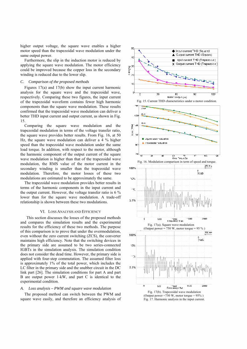
C. Comparison of the proposed methods Figures 17(a) and 17(b) show the input current harmonic analysis for the square wave and the trapezoidal wave, respectively. Comparing these two figures, the input current of the trapezoidal waveform contains fewer high harmonic components than the square wave modulation. These results confirmed that the trapezoidal wave modulation can deliver a better THD input current and output current, as shown in Fig. 15.
Comparing the square wave modulation and the trapezoidal modulation in terms of the voltage transfer ratio, the square wave provides better results. From Fig. 16, at 50 Hz, the square wave modulation can deliver a 4 % higher speed than the trapezoidal wave modulation under the same load torque. In addition, with respect to the motor, although the harmonic component of the output current of the square wave modulation is higher than that of the trapezoidal wave modulation, the RMS value of the motor current in the secondary winding is smaller than the trapezoidal wave modulation. Therefore, the motor losses of these two modulations are estimated to be approximately the same. The trapezoidal wave modulation provides better results in terms of the harmonic components in the input current and the output current. However, the voltage transfer ratio is 6 % lower than for the square wave modulation. A trade-off relationship is shown between these two modulations.
VI. LOSS ANALYSIS AND EFFICIENCY This section discusses the losses of the proposed methods
and compares the simulation results and the experimental results for the efficiency of these two methods. The purpose of this comparison is to prove that under the overmodulation, even without the zero current switching (ZCS), the converter maintains high efficiency. Note that the switching devices in the primary side are assumed to be two series-connected IGBTs in the simulation analysis. The simulation condition does not consider the dead time. However, the primary side is applied with four-step commutation. The assumed filter loss is approximately 1% of the total power, which includes the LC filter in the primary side and the snubber circuit in the DC link part [26]. The simulation conditions for part A and part B are output power 1-kW, and part C is identical to the experimental condition.
A. Loss analysis – PWM and square wave modulation The proposed method can switch between the PWM and
square wave easily, and therefore an efficiency analysis of
Fig. 15. Current THD characteristics under a motor condition.
Fig. 16. Modulation comparison in term of speed and torque.
Fig. 17(a). Square wave modulation
(Output power = 750 W, motor torque = 95 % )
Fig. 17(b). Trapezoidal wave modulation
(Output power =750 W, motor torque = 95% ) Fig. 17. Harmonic analysis in the input current.

these two modulations is needed. Figure 18 shows the loss comparison between the PWM and the square wave modulation. For the PWM, zero current switching can be applied in the primary side, and therefore the switching loss is zero. However, the PWM uses a 10-kHz carrier, which causes the high switching loss in the secondary side. On the other hand, for the square wave modulation, the switching loss is moved from the secondary side to the primary side because the switching in the secondary side only occurs at 120 degrees for each phase, following the square wave operation. Since the switching frequency is very low, the switching loss could be reduced to nearly zero. Furthermore, the frequency of the carrier does not affect the switching loss of the secondary side. However, the zero current switching cannot be applied, and so the IGBTs contain switching loss.
In PWM, the loss for the primary side is approximately 2.9% and that for secondary side is approximately 1.8%. As for the square wave modulation, the loss in the primary side is approximately 3.5%, and that in the secondary side is 1.1%. Based on these results, the losses between the PWM and square wave are found to be approximately the same.
B. Loss analysis – square wave modulation and trapezoidal trapezoidal modulation
The loss comparison between the square wave modulation and trapezoidal modulation is shown in Fig. 19. Note that the voltage and current of each modulation differ from each other, although the power is same for each modulation. For the square wave modulation, the input current Ir is 3.10 A (RMS), the output current Iu is 2.98 A (RMS), and the output phase voltage Vu is 120 V (RMS). For the trapezoidal modulation, the input current Ir is 3.00 A (RMS), the output current Iu is 3.05 A (RMS), and the output phase voltage Vu is 115 V (RMS).
The total loss for the square wave modulation is 45.30 W and that for the trapezoidal modulation is 45.18 W. The analysis reveals that these two modulations have similar losses under the same output power. Therefore, both modulations enable high efficiency.
C. Experimental efficiency This section describes the experimental efficiency of the
two proposed methods. The measurements are based on RL load condition and the parameters are the same as in Section V. First, the efficiency for the square wave modulation that includes the transition from PWM to the square wave is shown in Fig. 20. The output frequency ratio is shown at the bottom, where 1.0 = fa/ fo = 50 Hz/ 50 Hz (fa=actual output frequency, fo= design output frequency). In the graph, the area below 0.8 is for the PWM operation and the area for the square wave starts at 1.0. The efficiency remains constant at approximately 93.5%, even when the transition involves various power supplies.
Figure 21 shows the efficiencies for the square wave modulation and the trapezoidal modulation, as well as the simulation results for the square wave modulation.
Primary side Secondary sidePWM Square wave
Primary side0 Secondary side
Loss
[%]
1
3
2
4
5
Conduction loss
Recovery loss
Switching loss (Turn-on)
Switching loss (Turn-off)
Pout = 1000W
Fig. 18. Loss comparison between PWM and square wave modulation.
Fig. 19. Loss comparison between square wave and trapezoidal wave.
Fig. 20. Experimental efficiency of square wave with transition control.
Fig. 21. Comparison of efficiency. (Output frequency = 50Hz)

Simulation results A are for the theoretical calculation that shows only the switching device losses, and Simulation results B include the LC filter loss and the no-load test results with the switching devices losses. The no-load test results obtained from the prototype, including the possible losses occurring in the parasitic capacitor and the leakage current, are approximately 10 W. Both the experimental and simulation results reveal that the efficiency is approximately 93.5%.
VII. CONCLUSION Two overmodulation methods were proposed in an attempt
to improve the output-input voltage transfer ratio of an indirect matrix converter. The proposed methods are demonstrated through simulation and experimentally. The results of the present study confirm the validity of the proposed methods. The voltage transfer ratio is 0.97 for the square wave modulation and 0.92 for the trapezoidal wave modulation. Furthermore, both modulations can achieve efficiencies of up to 93.5% on average by using series-connected IGBTs in the primary side. In respect to the distortion in the input current, the LC filter needs to be redesigned to improve the THD in the future.
REFERENCES [1] Archarya, K.; Mazumder, S.K.; and Basu, I. “Reaching Criterion of a
Three-Phase Voltage-Source Inverter Operating with Passive and Nonlinear Loads and Its Impact on Global Stability”, IEEE Trans. on Industrial Electronics, Vol. 55, Issue.4, pp. 1795-1812, April 2008.
[2] Cruz, S.M.A.; and Ferreira, M. “Comparison between back-to-back and matrix converter drives under faulty conditions”, in 13h European Conference on Power Electronics and Applications, Barcelona, pp. 1-10, Sept. 2009.
[3] Sahoo, A.K.; Meenakshi, J.; Dash, S.S.; and Thyagarajan, T. “Analysis and simulation of matrix converter using PSIM”, in 7th international conference on ICPE Power Electronics, Daegu, pp. 414-419, Oct. 2007.
[4] Lixiang Wei; Lukaszeski, R.A and Lipo, T.A. “Analysis of Power-Cycling Capability of IGBT Modules in a Conventional Matrix Converter”, IEEE Trans. on Industry Applications, Vol. 45, Issue. 4, pp. 1443-1451, Aug. 2009.
[5] Bradaschia, F.; Cavalcanti, M.C.; Neves, F.; and de Souza, H. “A Modulation Techique to Reduce Switching Losses in Matrix Converters”, IEEE Trans. on Industrial Electronics, Vol. 56, Issue. 4, pp. 1186-1195, April 2009.
[6] Hojabri; H Mokhtari; and H Chang, L “A Generalized Technique of Modeling, Analysis and Control of a Matrix Converter Using SVD”, IEEE Trans. on Industrial Electronics, Vol. 99, pp.1-1, April 2010.
[7] Zanchetta, P.; Wheeler, P.W.; Clare, J.C.; Bland, M.; Empringham, L.; and Katsis, D. “Control Design of a Three-Phase Matrix-Converter-Based AC-AC Mobile Utility Power Supply”, IEEE Trans. on Industrial Electronics, Vol. 55, Issue.1, pp. 209-217, Jan. 2008.
[8] Friedli, T.; Round, S.D.; and Kolar, J.W. “A 100 kHz SiC Sparse Matrix Converter”, in IEEE Power Electronics Specialists Conf., Orlando, pp. 2148-2154, June 2007.
[9] Kolar, J.W.; Schafmeister, F.; Round, S.D.; and Erthl, H. “ Novel Three-Phase AC-AC Sparse Matrix Converters”, IEEE Trans. Power Electronics, Vol. 22, Issue. 5, pp.1649-1661, Sept. 2007.
[10] Gang Li; Kai Sun; and Lipei Huang, and Seiki Igarashi “RB-IGBT gate drive circuit and its application in two-stage matrix converter”, in 23rd Anuual APEC, Austin, pp. 245-251, Feb. 2008.
[11] Pena, R.; Cardenas, R.; Reyes, E.; Clare, J.; and Wheeler, P. “A Topology for Multiple Generation System with Doubly Fed Induction Machines and Indirect Matrix Converter”, IEEE Trans. on Industrial Electronics, Vol. 56, pp.4181-4193, Oct. 2009.
[12] Correa, P.; Rodriguez, J.; Rivera, M.; Espinoza, J.R.; and Kolar, J.W “Predictive Control of an Indirect Matrix Converter”, IEEE Trans. on Industrial Electronics, Vol. 56, Issue. 6, pp. 1847-1853, June 2009.
[13] Fedyczak, Z.; Szczesniak, P.; and Korotyeyev, I. “Generation of matrix-reactance frequency converters based on unipolar PWM AC matrix-reactance choppers”, in Power Electronics Specialists Conference, pp. 1821-1827, June 2008.
[14] Itoh, J. -i; Koiwa, K.; and Kato, K. “Input current stabilization control of a matrix converter with boost-up functionality”, in International Power Electronics Conference (IPEC), Sapporo, pp. 2708-2714, June 2010
[15] Mariethoz, S.; Wijekoon, T.; and Wheeler, P. “Analysis, control and comparison of hybrid two-stage matrix converters for increased voltage transfer ratio and unity power factor”, in Power Conversion Conference, Nagoya, pp. 43-50, April 2007.
[16] Kato, K.; and Itoh, J.-i. “Control strategy for a buck-boost type direct interface converter using an indirect matrix converter with an active snubber”, in Applied Power Electronics Conference and Exposition, Palm Springs, pp. 1684-1691, Feb. 2010.
[17] Satish, T.; Mohapatra, KK; and Mohan, N. “Steady State Over-Modulation of Matrix Converter Using Simplified Carrier Based Control”, in 33rd Annual Conference Industrial Electronics Society, Taipei, pp. 1817-1822, Nov. 2007.
[18] Jan, Bauer; Jiri, Lettl; Stanislav, Fligl; and Libor, Linhart. “Contribution to the matrix converter overmodulation strategies based on the virtual dc-link concept”, in 14th Power Electronics and Motion Control Conference, Macedonia, T3-46-T3-52, Sept. 2010.
[19] Thuta, S.; Mohapatra, K.K; and Mohan, N. “Matrix converter over-modulation using carrier- based control: Maximizing the voltage transfer ratio”, in IEEE Power Electronics Specialists Conf., Rhodes, pp. 1727-1733, June 2008.
[20] Goh Teck Chiang, Itoh, J.-i. “Votlage transfer ratio improvement of an Indirect Matrix Converter by Single pulse modulation”, in Energy Conversion Congress and Exposition, Atlanta, pp. 1830-1837, Sept. 2010.
[21] Tamai, Y.; Ohguchi, H.; Sato, I.; Odaka, A.; Mine, H.; and Itoh, J.-i. “A Novel Control Strategy for Matrix Converters in Over-modulation Range”, in Power Conversion Conference, Nagoya, pp. 1049-1055, April 2007.
[22] Schafmeister, F.; Herold, S.; and Kolar, J.W. “Evaluation of 1200 V-Si-IGBTs and 1300 V-SiC-JFETs for application in three-phase very sparse matrix AC-AC converter systems”, in Applied Power Electronics Conference and Exposition, Vol. 1, pp. 241-255, 2003.
[23] Lixiang Wei; Lipo, T.A; and Lukaszewski, R.A. “Comparison of IGBT cycling capabilities for different AC/AC topologies”, in IEEE Energy Conversion Congress and Exposition, San Jose, pp. 3298-3305, Sept. 2009.
[24] Goh Teck Chiang; and Itoh, J. –i. “DC/DC Boost Converter Functionality in a Three-Phase Indirect Matrix Converter”, IEEE Trans. on Power Electronics, Vol. 26, Issue. 5, pp. 1599-1607, May 2011.
[25] Itoh, J.-i.; and Ohtani, N. “Square wave operation for a single-phase PFC three-phase motor drive system without a reactor”, in International Conference ICEMS, Tokyo, pp. 1-2, Nov. 2009.
[26] Bernet, S.; Ponnaluri, S.; Teichmann, R. “Design and loss comparison of matrix converters, and voltage-source converters for modern AC drives”, IEEE Trans. on Industrial Electronics, Vol. 49, pp. 304, Apr. 2002.

Goh Teck Chiang (M’09) was born in Seremban,
Malaysia, in 1981. He received the B.S. degree in
electrical and electronic engineering from
Queensland University of Technology, Brisbane,
Australia in 2004 and the M.S. degree in electrical
and electronic engineering from Nagaoka
University of Technology, Japan in 2009, where
currently, he is working towards to the Ph.D. degree
in electrical and electronic engineering. His
research interests include indirect matrix converter, PWM and motor drives.
Jun-Ichi Itoh (M’01) was born in Tokyo, Japan, in
1972. He received the M.S. and Ph.D. degrees in
electrical and electronic systems engineering from
Nagaoka University of Technology, Niigata, Japan,
in 1996, 2000, respectively. From 1996 to 2004, he
was with Fuji Electric Corporate Research and
Development, Ltd., Tokyo, Japan. Since 2004, he
has been with Nagaoka University of Technology,
Niigata, Japan as Associate Professor. His research interests are matrix
converters, dc/dc converters, power factor correction techniques and motor
drives. Dr. Itoh received the IEEJ Academic Promotion Award (IEEJ
Technical Development Award) in 2007.