complex layered materials and periodic electromagnetic...
TRANSCRIPT

UNIVERSITY OF CALIFORNIA
Los Angeles
Complex Layered Materials and
Periodic Electromagnetic Band-Gap Structures: Concepts, Characterizations, and Applications
A dissertation submitted in partial satisfaction of the
requirements for the degree
Doctor of Philosophy in Electrical Engineering
by
Hossein Mosallaei
2001

© Copyright by
Hossein Mosallaei
2001


iii
To my wife, Afsaneh …
whose love, patient, and support made it all possible.

iv
Contents
Contents iv
List of Figures x
List of Tables xxviii
Acknowledgements xxx
Vita xxxi
Abstract xxxiv
1 Introduction 1
1.1 Optimal Composite Materials for RCS Reduction of Canonical Targets and
Design of High Performance Lens Antennas ………………………….…... 2
1.1.1 Vector Wave Solution/GA Technique ……………………………… 3
1.1.2 RCS Reduction of Canonical Targets ……………………………… 3
1.1.3 Design Optimization of the Non-Uniform Luneburg and 2-shell lens
Antennas ………………………………………………………….… 4
1.2 Broadband Characteristics of Periodic Electromagnetic Band-Gap Structures 7

v
1.2.1 FDTD Computational Engine …………………………………….… 7
1.2.2 Frequency Selective Surfaces ………………………………………. 8
1.2.3 Photonic Band-Gap Materials …………………………………….… 9
1.2.4 Composite Media with Negative Permittivity/Permeability ………... 10
2 Vector Wave Solution of Maxwell’s Equations Integrated with the Genetic
Algorithm 16
2.1 Vector Wave Solution of Maxwell’s Equations ………….…………………. 17
2.2 Genetic Algorithm Optimization Technique …………….………………….. 20
2.3 Modal Solution/GA in Presenting Novel Designs ……….…………………. 24
3 RCS Reduction of Canonical Targets using GA Synthesized RAM 25
3.1 Vector Wave Solution/GA Implementation ………………………….……... 28
3.2 Wide-Band Absorbing Coating for Planar Structures ……………….….…... 31
3.3 RCS Reduction of Cylindrical and Spherical Structures ……………………. 34
3.3.1 Monostatic RCS Reduction ……………………………………….… 34
3.3.2 Bistatic RCS Reduction and the Deep Shadow Region …………….. 37
3.4 GA with Hybrid Planar/Curved Surface Implementation …………………... 45
3.5 Summary ……………………………………………………………………. 49
4 Design Optimization of the Non-Uniform Luneburg and 2-Shell Lens
Antennas 51
4.1 Modal Solution Integrated with GA/Adaptive-Cost-Function …..………….. 53
4.2 Uniform Luneburg Lens Antenna and its Shortcomings …………..………... 55

vi
4.3 Non-Uniform Luneburg Lens Antenna ……………………………..………. 59
4.3.1 GA Implementation …………………………………………..……… 59
4.3.2 Non-Uniform Lens with Improved Gain ……………………..……… 60
4.3.3 High Gain/Low Sidelobe Non-Uniform Lens …………………..…… 61
4.3.4 Optimal Non-Uniform Lens with Feed Offset and Air Gap ……..….. 63
4.4 2-Shell Lens Antenna ……………………………………………………..… 71
4.5 Near Field Characteristics of the Lens Antenna …………………………..… 74
4.5.1 Focusing Behavior of the Luneburg Lens ………………………….... 75
4.5.2 Focusing Behaviors of the Constant and 2-Shell Lenses ………….… 75
4.6 Summary ……………………………………………………..……………... 79
5 Broadband Characterization of Complex EBG Structures 82
5.1 Analysis Technique …………………………………………………………. 83
5.1.1 Yee Algorithm …………………………..…………………………… 86
5.1.2 Total Field/Scattered Field Formulation ..…………………………… 86
5.1.3 Periodic Boundary Conditions ………….…………………………… 86
A. Sin/Cos Method …………………………………………………. 87
B. Split-Field Technique ……………………..…………………….. 88
B.1 Three-Dimensional Split-Field Formulations ……………... 89
B.2 Numerical Stability Analysis ……………………………… 95
5.1.4 Perfectly Matched Layer ……….……….…………………………… 96
A. Berenger’s PML Medium ……………………………………….. 97
B. Anisotropic PML Medium ………………………………………. 102

vii
C. Imposing PBC in the UPML Medium ……………..……………. 103
5.1.5 Prony’s Extrapolation Scheme ………………………………………. 106
5.2 Characterization of Challenging EBG Structures …………………………... 108
6 Frequency Selective Surfaces 110
6.1 Multi-Layered Planar Dielectric Structures ………………………………… 111
6.2 Double Concentric Square Loop FSS ……….……………………………… 114
6.3 Dipole FSS Manifesting High Q Resonance ...……………………………… 116
6.4 Patch FSS Manifesting High Q Resonance .....……………………………… 119
6.5 Crossed Dipole FSS ………………………….……………………………… 121
6.6 Dichroic Plate FSS …………………………..……………………………… 123
6.7 Inset Self-Similar Aperture FSS ……………..……………………………… 125
6.8 Fractal FSS …………………………………..……………………………… 127
6.9 Multi-Layered Tripod FSS …………………..……………………………… 130
6.10 9-Layer Dielectric/Inductive Square Loop FSS …………………………… 136
6.11 Smart Surface Mushroom FSS ………………..…………………………… 139
6.12 Summary …………………………………...……………………………… 143
7 Photonic Band-Gap Structures 144
7.1 Band-Gap Characterization of PBG ………………………………………… 145
7.1.1 Triangular PBG ………………………..…………………..………… 146
7.1.2 Rectangular PBG ……..………………..…………………..………… 146
7.1.3 Woodpile PBG ……………….………..…………………..………… 147

viii
7.1.4 Effective Dielectric Material …………..…………………..………… 148
7.2 Representative Applications of PBG ……………...………………………… 160
7.2.1 High Q Nanocavity Lasers …………………………………………... 160
A. PBG Cavity ……………………………………………………… 160
B. Effective Dielectric Cavity ……………………………………… 162
C. 7-Layer High Q PBG Structure …………………………………. 164
7.2.2 Guiding the EM Waves in Sharp Bends: Channelizing the Light ….... 171
A. Guiding the Waves at 90o and 60o Bends utilizing PBG …...…… 171
B. Guiding at the Sharp Corners based on the Effective Dielectric 173
7.2.3 Miniaturized Microstrip Patch Antennas …………………………..... 177
A. Microstrip Patch Antenna …………………………………..…… 178
B. PBG Substrate …………………………………………………… 180
C. Effective Dielectric Substrate …………………………………… 181
7.3 Summary ……………………………………………………………………. 189
8 Composite Media with Negative Permittivity and Permeability Properties 191
8.1 Electromagnetic Properties of LH Materials …...…………………………… 192
8.1.1 Reversal of the Doppler Shift ...………..…………………..………… 193
8.1.2 Anomalous Refraction ..………………..…………………..………… 193
8.1.3 Reversal of Radiation Pressure to Radiation Tension ……..………… 195
8.2 Characterization of LH Materials ……………....…………………………… 196
8.2.1 Conducting Straight Wires …...………..…………………..………… 196
8.2.2 Spilt Ring Resonators ..…….…………..…………………..………… 197

ix
8.2.3 Conducting Straight Wires/Split Ring Resonators …………...……… 198
8.3 Summary and Future Investigations …………....…………………………… 206
9 Summary and Suggestions for Future Work 207
9.1 Summary …………………………………….....…………………………… 207
9.2 Suggestions for Future Work ………......……..…………………..………… 209
A Electromagnetic Scattering from an Arbitrary Configuration of Eccentric
Spheres 213
A.1 Objective …………………………………….....…………………………… 213
A.2 Modal Solution of Eccentric Spherical Structures ……...………..………… 214
A.3 Boundary Conditions ……………………………….…...………..………… 216
A.3.1 Dyadic Green’s Second Theorem …...………..…………...………… 216
A.3.2 Spherical Translational Additional Theorems …...………..………… 219
A.3.3 Matrix Equations …………………....………..…………...………… 220
B FDTD/Prony for Efficient Analysis of Complex Periodic Structures 222
Bibliography 225

x
List of Figures
1.1 Vector wave solution of Maxwell’s equations integrated with the genetic
algorithm optimizer for designing optimal composite materials. ……..……… 5
1.2 Optimal RAM coatings for RCS reduction of canonical targets. …...…………. 6
1.3 Design optimization of the non-uniform lens antennas. ……...……..…………. 6
1.4 Schematic of the FDTD/Prony computational engine for characterizing
challenging EBG structures. …………………………………………………… 11
1.5 Different classes of FSS for various EM applications. …...…………………… 12
1.6 Different classes of PBG for various EM applications. ………...……………... 13
1.7 Potential applications of the PBG structures; high Q nanocavity lasers, guiding
the EM waves in sharp bends, and miniaturized microstrip patch antennas. ….. 14
1.8 Composite LH material with simultaneously negative
permittivity/permeability. ……………………………………………………… 15
2.1 Multi-layered canonical structures and their corresponding coordinates. ……... 17
2.2 Schematic of the tournament selection in the GA optimizer. ……...…………... 22
2.3 Single-point crossover operation in the GA optimizer. ……...………………… 23
2.4 Mutation operation in the GA optimizer. ………...……………………………. 23
2.5 Flowchart of the modal solution/GA optimization procedure. ……...…………. 24

xi
3.1 Flowchart of the genetic algorithm integrated with the vector wave solution of
Maxwell's equations for obtaining optimal RAM. Note the possibility of using
GA planar/curved surface implementation for initializing the population.
Coated planar, cylindrical and spherical targets with their appropriate
coordinate systems are also shown. ……………………………………………. 27
3.2 Relative permittivity and permeability of materials #7 and #16, from Table 3.1,
as a function of frequency. …………………………………………………….. 33
3.3 Reflection coefficient of the RAM coated conducting planar structure. (Note
that dB.0=Γ for the PEC) ……………………………………………………. 34
3.4 RCS of the conducting cylinder, without and with coating. RCS based on GO
formula is also shown. …………………………………………………………. 40
3.5 RCS of the conducting sphere, without and with coating. RCS based on GO
formula is also shown. …………………………………………………………. 40
3.6 Current distributions on the cylindrical structure for TMz and TEz modes,
compared with the spherical structure. Note the surface current flow on the
cylindrical structure for TEz mode has closer similarity to the nature of the
current flow on the spherical structure. ………………...……………………… 41
3.7 Bistatic RCS of the conducting cylinder (TEz case), without and with coating
(Table 3.3(a)): (a) o180=φ (monostatic), (b) o135=φ , (c) o90=φ , (d)
o45=φ , (e) o0=φ (forward scattering). ……………………………………… 42

xii
3.8 Bistatic RCS of the conducting cylinder (TEz case) in the deep shadow region
( o0=φ ), without and with coating (Table 3.3(b)). Optimal coating is
determined for the forward scattering. ………………………………………… 43
3.9 Bistatic RCS of the conducting sphere (E-plane), without and with coating
(Table 3.4(a)). (a) o180=θ (monostatic), (b) o135=θ , (c) o90=θ , (d)
o45=θ , (e) o0=θ (forward scattering). In order to show the range of RCS
variations, the dynamic range in these plots varies from dB60− to dB70 in
contrast to the cylindrical case with an dB80 dynamic range (Fig. 3.7). …..… 44
3.10 Bistatic RCS of the conducting sphere (E-plane) in the deep shadow region
( o0=θ ), without and with coating (Table 3.4(b)). Optimal coating is
determined for the forward scattering. ………………………………………… 45
3.11 Comparison of the RCS of the conducting sphere coated with the optimal
spherical coating (Table 3.4(a)), optimal planar coating (Table 3.2(a)), and
optimal spherical coating using GA hybrid planar/curved surface
implementation (Table 3.5). …………………………………………………… 48
3.12 Convergence curve of the GA hybrid planar/curved surface implementation
compared to the GA method for RCS reduction of the conducting sphere. …… 48
4.1 Genetic algorithm integrated with modal solution of Maxwell's equations for
designing optimum non-uniform lens antenna. ………………………………... 54
4.2 5-shell λ30 diameter Luneburg lens antenna. An end-fire antenna consisting of
four infinitesimal dipoles models the actual feed. ……………………………... 57

xiii
4.3 Radiation pattern of the feed antenna. Feed has cross polarization isolation
around dB17 with about 7% spill-over efficiency. …………………………… 58
4.4 Gain pattern of the λ30 diameter uniform Luneburg lens antenna in the zx −
plane. Note the appearance of the unwanted grating lobes for 5-shell case. …... 58
4.5 Gain pattern of the 5-shell λ30 diameter uniform and non-uniform optimized
lens antenna in the zx − plane. ( 0,1 == βα ) ………………………………... 66
4.6 Gain pattern of the 10-shell λ30 diameter uniform Luneburg lens antenna with
its sidelobe envelope function ( ) )(8.5log3812)( dBf ooθθ −= , in the zx −
plane. …………………………………………………………………………... 66
4.7 Comparison between 10-shell and 5-shell uniform design with the 5-shell non-
uniform optimized lens in the zx − plane. (adaptive cost function:
5.0,1 == βα ) …………………………………………………………………. 67
4.8 Gain pattern of the 5-shell non-uniform optimized lens using different
optimization parameters α and β . …………………………………………… 67
4.9 Convergence curve of the GA method for the 5-shell non-uniform optimized
lens using different optimization parameters α and β . ……………………… 68
4.10 Gain pattern of the 5-shell λ30 diameter non-uniform optimized lens antenna
in the zx − plane. Feed is positioned λ5.0 away the surface of the lens.
( 0,1 == βα and 5.0,1 == βα ) ……………………………………………… 68
4.11 Gain pattern of the 5-shell λ30 diameter non-uniform optimized lens antenna
with λ05.0 air gap in the zx − plane. ( 0,1 == βα and 5.0,1 == βα ) ……. 69

xiv
4.12 Gain pattern of the 5-shell λ30 diameter non-uniform optimized lens antenna
with λ05.0 air gap in the zx − plane. Feed is positioned λ5.0 away the
surface of the lens. ( 0,1 == βα and 5.0,1 == βα ) …………………………. 69
4.13 Gain pattern of the 5-shell λ30 diameter non-uniform optimized lens antenna
using 3-digit, 2-digit, and 1-digit accuracy in the dielectric constant rε , in the
zx − plane. ( 0,1 == βα ) ………………………………………….…………. 70
4.14 Co-polarization and cross polarization of the 5-shell λ30 diameter non-uniform
optimized lens antenna in the ,45,0 oo == φφ and o90=φ planes.
( 0,1 == βα ) …………………………………………………………………... 70
4.15 Geometrical optic theory applied to a relatively high dielectric 2-shell lens
antenna. ………………………………………………………………………… 73
4.16 Gain patterns of the λ30 diameter optimized 2-shell and homogeneous
( 315.3=rε ) lens antennas in the zx − plane. ( 0,1 == βα and
5.0,1 == βα ) …………………………………………………………………. 74
4.17 Gain pattern of the 5-shell λ30 diameter non-uniform spherical lens antenna in
the zx − plane using the optimal material and thickness determined from the
optimization of the cylindrical lens (Table 4.8). ( 0,1 == βα ) ……………….. 77
4.18 Near field contour plot of the 5-shell λ30 diameter non-uniform cylindrical
Luneburg lens antenna. (material and thickness are the same as the optimized
5-shell spherical lens (Table 4.2(a))) …………………………………………... 78

xv
4.19 Near field contour plot of the λ30 diameter constant cylindrical lens antenna.
(material and thickness are the same as the constant spherical lens,
( 315.3=rε )) …………………………………………………………………... 78
4.20 Near field contour plot of the 2-shell λ30 diameter cylindrical lens antenna.
(material and thickness are the same as the optimized 2-shell spherical lens
(Table 4.6(a))) …………………………………………………………………. 79
5.1 Powerful and efficient computational engine utilizing FDTD technique in the
characterization of complex periodic EBG structures. ………………………… 85
5.2 Periodic unit cell in the y direction for the sin/cos method. …………………… 87
5.3 Scattering of the plane wave by a periodic structure in the y and z directions:
(a) Propagation direction and polarization of the incident wave, (b) Geometry
of the structure, (c) Unit cell of the structure terminated to the PBC/PML walls. 89
5.4 Upper-right part of the computational domain surrounded by the PML layers.
The PML is truncated by the PEC. …………………………………………...... 101
6.1 5-Layer dielectric structure: (a) Infinite size dielectric in the y-z directions, (b)
Unit cell of the structure truncated to the PBC/PML walls. …………………… 112
6.2 Normal incidence reflection coefficient of the multi-layered dielectric
structure. FDTD compared to the analytic vector wave solution. ……...……… 112
6.3 o60 oblique incidence reflection coefficient of the multi-layered dielectric
structure. FDTD compared to the analytic vector wave solution (TE case). ….. 113

xvi
6.4 o60 oblique incidence reflection coefficient of the multi-layered dielectric
structure. FDTD compared to the analytic vector wave solution (TM case). …. 113
6.5 Double concentric square loop FSS: (a) Periodic structure, (b) Unit cell of the
structure. ……………………………………………………………………….. 115
6.6 Normal incidence reflected power of the double concentric square loop FSS.
FDTD/Prony compared to the split-field, sin/cos, and MoM techniques [9]. ..... 115
6.7 o60 oblique incidence reflected power of the double concentric square loop
FSS. FDTD/Prony compared to the split-field, sin/cos, and MoM techniques
(TM case) [9]. ……………………...…………………………………………... 116
6.8 Dipole FSS manifesting high Q resonance: (a) Periodic structure, (b) Unit cell
of the structure. Note that the PBC walls are positioned on the PEC edges. ….. 118
6.9 Normal and oblique incidence reflection coefficient of the dipole FSS. Note the
anomalous behavior around the λ−1 dipole length for the o1 tilt angle along
the length. ……………………………….………..……………………………. 118
6.10 Resonance behavior of the λ−1 dipole FSS for the o1 oblique incidence wave
(tilt along the length of dipoles). The performance is presented in an expanded
range around the resonance frequency. ………………………………………... 119
6.11 Square patch FSS manifesting high Q resonance: (a) Periodic structure, (b)
Unit cell of the structure. ………………………………………………………. 120
6.12 Normal and oblique incidence reflection coefficient of the patch FSS. Note the
anomalous behavior around the λ−21 patch size for the o1 oblique incidence. 120

xvii
6.13 Resonance behavior of the λ−21 patch FSS for the o1 oblique incidence
wave. The performance is presented in an expanded range around the
resonance frequency. …………………………………………………………... 121
6.14 Crossed dipole FSS: (a) Periodic structure, (b) Unit cell of the structure. Note
that the PBC walls are positioned on the dielectric sides. ……………………... 122
6.15 o30 oblique incidence transmission coefficient of the crossed dipole FSS. Note
the good agreement with the measurement data [56]. …………………………. 122
6.16 Dichroic plate FSS: (a) Periodic structure, (b) Unit cell of the structure. Note
that the PBC walls are positioned on the PEC edges. …………………………. 123
6.17 Normal and o30 oblique (TE/TM) incidence reflection coefficient of the
dichroic plate FSS. …………………………………………………………….. 124
6.18 Performance of the dichroic plate FSS in the expanded frequency range
GHz3631− for the normal and o30 oblique (TE/TM) incidence plane waves. 124
6.19 Inset self-similar aperture FSS: (a) Periodic structure, (b) Unit cell of the
structure. Note that the PBC walls are positioned on the PEC/dielectric sides. .. 126
6.20 Normal incidence transmission coefficient of the square patch, square aperture,
and inset self-similar aperture based on the FDTD compared to the
measurement data. ……………………………………………………………... 126
6.21 TE/TM o30 oblique incidence transmission coefficient of the inset self-similar
aperture FSS. ………………………………………………………………...… 127

xviii
6.22 Sierpinski fractal FSS: (a) Free standing fractal, (b) Dielectric backed fractal,
(c), (d) Unit cells of the structures. Note that the PBC walls are positioned on
the sides of the structures. ……………………………………………………... 129
6.23 Normal incidence transmission coefficient of the free standing Sierpinski
fractal FSS. …………………………………………………………………….. 129
6.24 Normal and o30 oblique incidence transmission coefficient of the dielectric
backed Sierpinski fractal FSS. …………………………………………………. 130
6.25 1-Layer tripod structure: (a) Free standing tripod, (b) Dielectric backed tripod,
(c), (d) Unit cells of the structures. Note that the PBC walls are positioned on
the sides of the structures. ……………………………………………………... 132
6.26 Normal and o30 oblique (TE/TM) incidence reflected power of the 1-layer
tripod FSS. ……………………………………………………………………... 133
6.27 Normal incidence transmission coefficient of the 1-layer tripod FSS printed on
the dielectric substrate. ………………………………………………………… 133
6.28 2-Layer tripod structure: (a) Periodic structure, (b) Unit cell of the structure.
Note that the PBC walls are positioned on the PEC edges. …………………… 134
6.29 Normal and o30 oblique (TE/TM) incidence reflected power of the 2-layer
tripod FSS. ……………………………………………………………………... 134
6.30 4-Layer tripod structure (composition of two sets of the structure shown in Fig.
6.28): (a) Periodic structure, (b) Unit cell of the structure. Note that the PBC
walls are positioned on the PEC edges. ………………………………………... 135

xix
6.31 Normal and o30 oblique (TE/TM) incidence reflected power of the 4-layer
tripod EBG structure. ………………………………………………………….. 135
6.32 9-Layer dielectric/inductive square loop FSS: (a) 2-Layer inductive square
loop, (b) 7-Layer dielectric material, (c) Composite square loop/dielectric
material (9 layers), (d) Cross section of the layered structure, (e) Unit cell of
the square loop FSS. ………………………..………………………………….. 137
6.33 Normal and o30 oblique (TE/TM) incidence transmission coefficient of the 2-
layer inductive square loop FSS. ………………………………………………. 138
6.34 Normal and o30 oblique (TE/TM) incidence transmission coefficient of the 7-
layer dielectric material. ……………………………………………………….. 138
6.35 Normal and o30 oblique (TE/TM) incidence transmission coefficient of the 9-
layer dielectric/inductive square loop FSS. ……………………………………. 139
6.36 Mushroom EBG: (a) Periodic structure, (b) Unit cell of the structure. Note that
the PBC walls are positioned on the PEC edges. ……………………………… 141
6.37 Normal and oblique incidence reflection phase of the mushroom EBG
structure. Note the phase variation from PEC to PMC. Reflection phase is
computed on the surface of mushrooms. ……….…………………….………… 141
6.38 Suppression of the surface waves: (a) 2-Layer mushroom EBG, (b) PEC
grating layers. Note that the structures are periodic in the y-z directions. …..… 142
6.39 Normal and oblique incidence reflection coefficient of the 2-layer mushroom
EBG structure. Notice that the mushroom EBG opens up a complete surface
waves band-gap region. ………………………………………………...……… 142

xx
7.1 Pictorially illustration of the (a) TE ( zE ), and (b) TM ( zH ) waves definitions
for a 2-D triangular PBG structure including of 5-layer dielectric columns. ..… 150
7.2 2-D triangular PBG structure including of 5-layer dielectric columns (finite in x
direction, infinite in y-z directions): (a) Periodic structure, (b) Unit cell of the
structure. Note that the PBC walls are positioned on the dielectric sides. …..… 151
7.3 Normal and oblique incidence reflection coefficient of the triangular PBG of
dielectric columns. The isolated dielectric regions open up the TE ( zE ) band-
gap. …………………………………………………………………...………... 151
7.4 2-D triangular PBG structure including of 5-layer air holes (finite in x
direction, infinite in y-z directions): (a) Periodic structure, (b) Unit cell of the
structure. Note that the PBC walls are positioned on the dielectric sides. …..… 152
7.5 Normal and oblique incidence reflection coefficient of the triangular PBG of
air holes. The connected dielectric regions open up the TM ( zH ) band-gap. … 152
7.6 2-D rectangular PBG structure including of 5-layer dielectric columns (finite in
x direction, infinite in y-z directions): (a) Periodic structure, (b) Unit cell of the
structure. Note that the PBC walls are positioned on the dielectric sides. …..… 153
7.7 Normal and oblique incidence reflection coefficient of the rectangular PBG of
dielectric columns. The isolated dielectric regions open up the TE ( zE ) band-
gap. …………………………………………………………………………….. 153
7.8 2-D rectangular PBG structure including of 5-layer air holes (finite in x
direction, infinite in y-z directions): (a) Periodic structure, (b) Unit cell of the
structure. Note that the PBC walls are positioned on the dielectric sides. …….. 154

xxi
7.9 Normal and oblique incidence reflection coefficient of the rectangular PBG of
air holes. The connected dielectric regions open up the TM ( zH ) band-gap. .... 154
7.10 2-D rectangular PBG structure including of 5-layer large size air holes (finite
in x direction, infinite in y-z directions): (a) Periodic structure, (b) Transverse
plane representing the dielectric spots surrounded by the air holes, (c) Unit cell
of the structure. Note that the PBC walls are positioned on the dielectric sides. 155
7.11 Normal and oblique incidence reflection coefficient of the rectangular PBG of
air holes. The large size of the air holes generates the isolated dielectric
columns opening up the TE ( zE ) band-gap. ………………………………...… 155
7.12 2-Layer square dielectric rods woodpile PBG structure (finite in x direction,
infinite in y-z directions): (a) Periodic structure, (b) Unit cell of the structure.
Note that the PBC walls are positioned on the dielectric sides. ……………..… 156
7.13 Normal and oblique incidence reflection coefficient of the square dielectric
rods woodpile PBG. Proper arrangements of the isolated and connected
dielectric regions open up an almost complete band-gap. ………...…………… 156
7.14 o30 incidence reflection phase of the square dielectric rods woodpile PBG.
Reflection phase is computed on the surface of structure. Notice that the phase
has an almost linear frequency variation within the band-gap. …………...…… 157
7.15 Effective dielectric model for composite periodic structure of air/dielectric
regions: (a) Periodic structure, (b) Effective dielectric material. ……………… 157

xxii
7.16 Multi-layered one-dimensional periodic dielectric structure (finite in x
direction, infinite in y-z directions). Effective dielectric model for the isolated
columns rectangular PBG in Fig. 7.6. …………………………………………. 158
7.17 Comparative study between the performance of triangular and rectangular
isolated columns PBG with the effective dielectric model for the o60 oblique
incidence TE wave ( zE ). ……………………………………………………… 158
7.18 Multi-layered one-dimensional periodic dielectric structure (finite in x
direction, infinite in y-z directions). Effective dielectric model for the
connected lattice rectangular PBG in Fig. 7.8. ………………………………… 159
7.19 Comparative study between the performance of triangular and rectangular
connected lattice PBG with the effective dielectric model for the o60 oblique
incidence TM wave ( zH ). ……………………………………………………... 159
7.20 Cavity design using finite thickness 2-D triangular PBG structure: (a) 3-D
geometry, (b) Cross section of the PBG (x-y plane). …………………………... 166
7.21 Near field patterns of the PBG: (a) Transverse plane, (b) Vertical plane. …….. 166
7.22 Effective dielectric model for the PBG periodic structure. ……...…………….. 166
7.23 Near field patterns of the effective dielectric as it models the PBG (inside the
band-gap): (a) Transverse plane, (b) Vertical plane. Note the lack of similarity
between the field patterns of effective dielectric and PBG (Fig. 7.21(a)) in
transverse plane. ……………………………………………………………….. 167
7.24 Near field patterns of the (a) PBG (outside the band-gap) compared to the (b)
effective dielectric. Note the similarity between the field patterns. …………… 167

xxiii
7.25 Near field pattern of the effective dielectric material in the transverse plane
with a relatively high dielectric defect region. The waves are almost confined
inside the cavity. ……………………………………………………………….. 168
7.26 Total stored energy inside the defect region for the PBG compared to the
effective dielectric materials. Note that the PBG has the highest quality factor. 168
7.27 High Q nanocavity laser utilizing 7-layer PBG structure. ……………………... 169
7.28 Total stored energy inside the defect region of the 7-layer PBG for the same
and different defect dielectrics (compared to the host medium). ………….…... 169
7.29 Defect band frequency of the 7-layer PBG for various defect dielectrics. …….. 170
7.30 Total Q of the 7-layer PBG versus normalized frequency (varying defect
dielectric). Notice that the maximum Q ( 1050=Q ) occurs around the
normalized frequency 346.00 =λa ( 0.4=defε ). …………………………….. 170
7.31 PBG for guiding the waves in o90 bend: (a) Cross section of the structure, (b)
Near field pattern. ……………………………………………………………… 175
7.32 PBG for guiding the waves in o60 bend: (a) Cross section of the structure, (b)
Near field pattern. ……………………………………………………………… 175
7.33 PBG for guiding the waves in o60 shaped bend utilizing two small holes: (a)
Cross section of the structure, (b) Near field pattern. Notice that the small holes
extremely improve the coupling of the waves in the corner (compared to the
Fig. 7.32(b)). …………………………………………………………………… 176

xxiv
7.34 PBG for guiding the waves in o60 shaped bend utilizing one big hole: (a)
Cross section of the structure, (b) Near field pattern. Notice that the structure
has almost the similar performance as the structure in Fig. 7.33(a). ………...… 176
7.35 Effective dielectric for guiding the waves in o90 bend: (a) Cross section of the
structure, (b) Near field pattern. Notice that the structure cannot turn the waves
similar to the PBG (Fig. 7.31(b)). …………………………………………...… 177
7.36 Patch antenna on the conventional substrate. Note to the edge
diffraction/scattered and space waves. ………………………………………… 183
7.37 Return loss ( 11S ) of the patch antenna on the conventional thin, thick, PBG,
and effective dielectric substrates. …………………………..……………..…... 183
7.38 Performance of the patch antenna on the conventional thin substrate, (a) Near
field pattern, (b) Far field patterns. …………………………………………….. 184
7.39 Performance of the patch antenna on the conventional thick substrate, (a) Near
field pattern, (b) Far field patterns. Note the pattern bifraction near o0=θ and
high back radiation. ………………...………………………………………….. 184
7.40 5-Layer photonic cells rectangular PBG of infinite air holes. …………………. 185
7.41 Band-gap region of the dielectric PBG for the waves propagating through the
PBG. …………………………………………………………………………… 185
7.42 Exploring the possibility of suppression the surface waves: (a) 5-Layer finite
thickness PBG, (b) PEC grating layers. Note that the structures are periodic in
the y-z directions. ………………………………………………………………. 186

xxv
7.43 Band-gap region of the dielectric PBG for the surface waves propagating in the
transverse plane. Note that the PBG is not able to generate any complete
surface wave band-gap. ………………………………………………………... 186
7.44 Patch antenna on the PBG substrate: (a) 3-D geometry, (b) Cross section of the
PBG (x-y plane). ……………………………………………………………….. 187
7.45 Performance of the patch antenna on the PBG substrate, (a) Near field pattern,
(b) Far field patterns. …………………………………………………………... 187
7.46 Patch antenna on the effective dielectric substrate. ……………………………. 188
7.47 Performance of the patch antenna on the effective dielectric substrate, (a) Near
field pattern, (b) Far field patterns. …………………………………………….. 188
8.1 Reflection and refraction of the EM waves on the boundary between the
right/left-handed materials. ……………………………………………………. 194
8.2 The point source radiation, (a) is diverged by the flat slab RH material, and (b)
is focused by the flat slab LH material provided it is thick enough. …………... 195
8.3 Electromagnetic performances of the media having (a) negative effective
permittivity, (b) negative effective permeability, and (c) both negative effective
permittivity/permeability. ……………………………………………………… 199
8.4 2-Layer conducting straight wires: (a) Periodic structure, (b) Unit cell of the
structure. Note that the PBC walls are positioned on the PEC edges. ………… 200
8.5 Normal and o30 oblique incidence reflected power of the straight wires.
Negative effective permittivity of the structure creates the dielectric gap region. 200

xxvi
8.6 2-Layer split ring resonators ( ||H ): (a) Periodic structure, (b) Unit cell of the
structure. ……………………………………………………………………….. 201
8.7 Normal and o30 oblique incidence reflected power of the SRR ( ||H ). Negative
effective permeability of the structure creates the magnetic gap regions. ..…… 201
8.8 2-Layer split ring resonators ( ⊥H -same dimensions as ||H case): (a) Periodic
structure, (b) Unit cell of the structure. ………………………………………... 202
8.9 Normal and o30 oblique incidence reflected power of the SRR ( ⊥H ). Negative
effective permittivity of the structure creates the dielectric gap regions. ...…… 202
8.10 Composite material of 2-layer straight wires/split ring resonators ( ||H ): (a)
Periodic structure, (b) Unit cell of the structure. Note that the PBC walls are
positioned on the PEC edges. ………………………………………………….. 203
8.11 Normal and o30 oblique incidence reflected power of the straight wires/SRR
( ||H ). Negative effective permittivity of the straight wires are combined with
the negative effective permeability of the SRR ( ||H ) to present the LH material
around the frequency GHz3.5 (pass-band region). …………………………… 203
8.12 Illustration of the LH material with negative permittivity/permeability. The
pass-band occurs within the dielectric/magnetic gap regions of the straight
wires/SRR. …………………………………………………………...………… 204
8.13 Composite material of 2-layer straight wires/split ring resonators ( ⊥H ): (a)
Periodic structure, (b) Unit cell of the structure. Note that the PBC walls are
positioned on the PEC edges. ………………………………………………….. 205

xxvii
8.14 Normal and o30 oblique incidence reflected power of the straight wires/SRR
( ⊥H ). The SRR ( ⊥H ) has the positive permeability and no LH property can be
achieved. Notice that the pass-band occurs where the composite material has
the positive effective permittivity/permeability. ….…………………………… 205
A.1 Configuration of N eccentric spheres and their corresponding coordinates. …... 214
B.1 Double concentric square loop FSS: (a) Periodic structure, (b) Unit cell of the
structure. ……………………………………………………………………….. 223
B.2 Normal incidence scattered field of the double concentric square loop FSS in
the time domain. A comparative study between FDTD and FDTD/Prony. …… 224
B.3 Normal incidence reflected power of the double concentric square loop FSS in
the frequency domain. A comparative study between FDTD and FDTD/Prony. 224

xxviii
List of Tables
3.1 Relative permittivities and permeabilities of the 16 materials in the database
[22]. ……………………………………………………………………………. 30
3.2 Optimum RAM for the conducting plane, (a) 2)(2.0 ≤≤ GHzf opt , (b)
10)(2.0 ≤≤ GHzf opt . ……………………………………………………..…… 33
3.3 Optimum RAM for the cm148 diameter conducting cylinder
( 2)(2.0 ≤≤ GHzfopt ), (a) Monostatic ( o180=φ ), (b) Bistatic ( o0=φ ). ……… 39
3.4 Optimum RAM for the cm148 diameter conducting sphere
( 2)(2.0 ≤≤ GHzf opt ), (a) Monostatic ( o180=θ ), (b) Bistatic ( o0=θ ). …...… 39
3.5 Optimum RAM designed by GA hybrid planar/curved surface implementation
for the cm148 diameter conducting sphere ( 2)(2.0 ≤≤ GHzf opt ). (monostatic
case) ……………………………………………………………………………. 47
4.1 Design parameters of a 5-shell λ30 diameter uniform Luneburg lens antenna. 57
4.2 Design parameters of a 5-shell λ30 diameter non-uniform Luneburg lens
antenna, (a) 0,1 == βα , (b) 5.0,1 == βα . ………………………………..… 65

xxix
4.3 Design parameters of a 5-shell λ30 diameter non-uniform Luneburg lens
antenna. Feed is positioned λ5.0 away the surface of the lens, (a) 0,1 == βα ,
(b) 5.0,1 == βα . ……………………………………………………………… 65
4.4 Design parameters of a 5-shell λ30 diameter non-uniform Luneburg lens
antenna with λ05.0 air gap, (a) 0,1 == βα , (b) 5.0,1 == βα . …………..… 65
4.5 Design parameters of a 5-shell λ30 diameter non-uniform Luneburg lens
antenna with λ05.0 air gap. Feed is positioned λ5.0 away the surface of the
lens, (a) 0,1 == βα , (b) 5.0,1 == βα . …………………………………...…. 65
4.6 Design parameters of a 2-shell lens antenna, (a) 0,1 == βα , (b)
5.0,1 == βα . …………………………………………………………………. 73
4.7 Frequency dependency of the 2-shell and 5-shell optimized lens antennas.
( 0,1 == βα ) ………………………...………………………………………... 73
4.8 Design parameters of a 5-shell λ30 diameter non-uniform cylindrical
Luneburg lens antenna. ( 0,1 == βα ) ………………………………...………. 77

xxx
ACKNOWLEDGEMENTS
This research would not have been possible without the support given to me by my
relatives, friends, and colleagues. I first would like to thank my committee and in
particular Professor Yahya Rahmat-Samii, committee chair, for his encouragements and
excellent advises.
I thank my family, which have given tremendous support and guidance through
my life to get me this far. Special thanks to my wife Afsaneh for her sacrifices during
these years and for her love and support. Without the understanding and support of my
wife, this work would not have been possible.
Finally, and foremost, I offer thanks to God. It is only by God’s grace and
guidance that this work and all my endeavors are possible.

xxxi
VITA
July 8, 1968 Born, Abadan, Iran. 1991 B.S. in Electrical Engineering Shiraz University, Shiraz, Iran.
1994 M.S. in Electrical Engineering Shiraz University, Shiraz, Iran.
1991-1996 Teaching Assistant Shiraz University, Shiraz, Iran.
1997-Present Graduate Student Researcher University of California, Los Angeles.
1999-2000 Teaching Assistant University of California, Los Angeles.
1994 Outstanding M.S. Student Award Shiraz University, Shiraz, Iran. 1995 First Rank in Electromagnetics National Entrance Exam Ministry of Culture and Higher Education, Iran. 1997-1998 Graduate Fellowship Award University of California, Los Angeles. 2000 Second Best Student Paper IEEE Award APS/URSI International Symposium, Salt Lake City.
2001 URSI Young Scientist Award URSI International Symposium on Electromagnetic Theory, Victoria, Canada.
PUBLICATIONS AND PRESENTATIONS
H. Mosallaei, and Y. Rahmat-Samii, “Grand challenges in analyzing EM band-gap structures: An FDTD/Prony technique based on the split-field approach,” IEEE AP-S International Symposium, Boston, Massachusetts, July 8-13, 2001.

xxxii
H. Mosallaei, and Y. Rahmat-Samii, “Composite materials with negative permittivity and permeability properties: Concept, analysis, and characterization,” IEEE AP-S International Symposium, Boston, Massachusetts, July 8-13, 2001. H. Mosallaei, and Y. Rahmat-Samii, “Characterization of complex periodic structures: FDTD analysis based on Sin/Cos and Split-Field approaches,” URSI International Symposium on Electromagnetic Theory, Victoria, Canada, May 13-17, 2001. (Young Scientist Award) H. Mosallaei, and Y. Rahmat-Samii, “PBG/Periodic structures in electromagnetics: Nanocavities, waveguides, and patch antennas,” URSI International Symposium on Electromagnetic Theory, Victoria, Canada, May 13-17, 2001. Y. Rahmat-Samii, and H. Mosallaei, “Electromagnetic band-gap structures: Classification, characterization, and applications,” 11’th International Conference on Antennas and Propagation, UMIST, Manchester, UK, Apr. 17-20, 2001. (Invited Talk) H. Mosallaei, and Y. Rahmat-Samii, “Nanocavities, waveguides, and miniaturized patch antennas designed by PBG and effective dielectric materials: A comparative study,” National Radio Science Meeting, Boulder, Colorado, Jan. 8-11, 2001. H. Mosallaei, and Y. Rahmat-Samii, “Non-uniform Luneburg and 2-shell lens antennas: Radiation characteristics and design optimization,” IEEE Trans. Antennas Propagat., vol. 49, no. 1, pp. 60-69, Jan. 2001. H. Mosallaei, and Y. Rahmat-Samii, “RCS reduction of canonical targets using genetic algorithm synthesized RAM,” IEEE Trans. Antennas Propagat., vol. 48, no. 10, pp. 1594-1606, Oct. 2000. (Memory of James Wait) H. Mosallaei, and Y. Rahmat-Samii, “GA optimized Luneburg lens antennas: Characterizations and measurements,” ISAP, Fukuoka, Japan, Aug. 21-25, 2000. H. Mosallaei, and Y. Rahmat-Samii, “Photonic Band-Gap (PBG) versus effective refractive index: A case study of dielectric nanocavities,” IEEE AP-S International Symposium, Salt Lake City, Utah, July 16-21, 2000. (IEEE Student Award) Y. Rahmat-Samii, H. Mosallaei, and Z. Li, “Luneburg lens antennas revisited: Design, optimization, and measurements,” IEEE Millennium Conference on Antennas & Propagation, Davos, Switzerland, Apr. 9-14, 2000. H. Mosallaei, M. Chatterji, and Y. Rahmat-Samii, “EM field characterization in two-dimensional photonic crystals: FDTD parametric analysis and design optimization,” Photonic Band Engineering, MURI review, Nov. 18, 1999.

xxxiii
H. Mosallaei, and Y. Rahmat-Samii, “Non-uniform Luneburg lens antennas: A design approach based on genetic algorithms,” IEEE AP-S International Symposium, Orlando, Florida, July 11-16, 1999. H. Mosallaei, and Y. Rahmat-Samii, “RCS reduction in planar, cylindrical and spherical structures by composite coatings using genetic algorithms,” IEEE AP-S International Symposium, Orlando, Florida, July 11-16, 1999. H. Mosallaei, and Y. Rahmat-Samii, “Optimum design of non-uniform Luneburg lens antennas: Genetic algorithm with adaptive cost function,” ACES, Monterey, California, Mar. 15-19, 1999. Y. Rahmat-Samii, R. A. Hoferer, and H. Mosallaei, “Beam efficiency of reflector antennas: the simple formula,” IEEE Antennas Propagat. Mag., vol. 40, no. 5, pp. 82-87, Oct. 1998.

xxxiv
ABSTRACT OF THE DISSERTATION
Complex Layered Materials and
Periodic Electromagnetic Band-Gap Structures: Concepts, Characterizations, and Applications
by
Hossein Mosallaei
Doctor of Philosophy in Electrical Engineering
University of California, Los Angeles, 2001
Professor Yahya Rahmat-Samii, Chair
The main objective of this dissertation is to characterize and create insight into the
electromagnetic performances of two classes of composite structures, namely, complex
multi-layered media and periodic Electromagnetic Band-Gap (EBG) structures. The
advanced and diversified computational techniques are applied to obtain their unique
propagation characteristics and integrate the results into some novel applications.
In the first part of this dissertation, the vector wave solution of Maxwell’s
equations is integrated with the Genetic Algorithm (GA) optimization method to provide
a powerful technique for characterizing multi-layered materials, and obtaining their
optimal designs. The developed method is successfully applied to determine the optimal
composite coatings for Radar Cross Section (RCS) reduction of canonical structures.
xxxv
Both monostatic and bistatic scatterings are explored. A GA with hybrid planar/curved
surface implementation is also introduced to efficiently obtain the optimal absorbing
materials for curved structures. Furthermore, design optimization of the non-uniform
Luneburg and 2-shell spherical lens antennas utilizing modal solution/GA-adaptive-cost
function is presented. The lens antennas are effectively optimized for both high gain and
suppressed grating lobes.
The second part demonstrates the development of an advanced computational
engine, which accurately computes the broadband characteristics of challenging periodic
electromagnetic band-gap structures. This method utilizes the Finite Difference Time
Domain (FDTD) technique with Periodic Boundary Condition/Perfectly Matched Layer
(PBC/PML), which is efficiently integrated with the Prony scheme. The computational
technique is successfully applied to characterize and present the unique propagation
performances of different classes of periodic structures such as Frequency Selective
Surfaces (FSS), Photonic Band-Gap (PBG) materials, and Left-Handed (LH) composite
media. The results are incorporated into some novel applications such as high Q
nanocavity lasers, guiding the electromagnetic waves at sharp bends, and miniaturized
microstrip patch antennas.

1
Chapter 1
Introduction
Many of novel technological designs have resulted by analyzing the properties of
materials and proposing new structural configurations for them. Multi-layered and
periodic dielectric/metallic structures are two types of composite media with the potential
applications in Electromagnetics (EM). Utilizing these materials one can effectively
control the propagation of EM waves and present the novel designs. In order to develop a
new structural configuration with unique properties, one needs to thoroughly understand
the characteristics of the structure. This can be accomplished by applying an advanced
computational engine.
The materials presented in this dissertation will provide a comprehensive
description of two classes of structures, namely, complex multi-layered media and
periodic Electromagnetic Band-Gap (EBG) structures. The objective is to analyze
theoretically/numerically their interaction with electromagnetic waves, identify their
innovative propagation characteristics, and incorporate the results into some novel
applications.
To accomplish this, two potentially powerful computational techniques, as
outlined below, are developed

2
(a) Vector wave solution of Maxwell’s equations integrated with the Genetic Algorithm
(GA) optimizer for characterizing layered composite materials,
(b) Finite Difference Time Domain (FDTD) technique with Periodic Boundary
Condition/Perfectly Matched Layer (PBC/PML) integrated with the Prony scheme to
efficiently construct the broadband performance of the periodic band-gap structures.
The developed computational engines are successfully incorporated into the
following areas of interest
• Radar Cross Section (RCS) reduction of canonical targets,
• Non-Uniform Luneburg and 2-Shell lens antennas,
• Frequency Selective Surfaces (FSS),
• Photonic Band-Gap (PBG) materials and their potential applications,
• Composite media with negative permittivity/permeability.
In the following sections, each of the above-itemized areas of research is briefed
with the research goals of each listed.
1.1 Optimal Composite Materials for RCS Reduction of Canonical
Targets and Design of High Performance Lens Antennas
The focus is to integrate the modal solution of Maxwell’s equations with the Genetic
Algorithm (GA) to present the optimal composite materials for two classes of
applications namely, (a) Radar Cross Section (RCS) reduction of canonical targets, and
(b) design optimization of the non-uniform Luneburg and 2-shell lens antennas. The
analysis technique and design optimization of the layered structures are addressed.

3
1.1.1 Vector Wave Solution/GA Technique
To obtain the electromagnetic performance of complex multi-layered materials such as
planar, cylindrical, or spherical structures, the vector wave solution of Maxwell’s
equations is applied to accurately determine the modal solution in their corresponding
coordinate systems [1]-[3].
Next the modal solution is integrated with the GA technique to present the
optimal composite layered structure. The GA technique is a global optimizer, and is very
efficient in optimizing the new electromagnetic problems having discontinuities,
constrained parameters, discrete solution domains, and a large number of dimensions
with many local optima [4].
An accurate and capable computer code is developed to integrate the modal
solution with the GA technique effectively. Fig. 1.1 shows the schematic of the
computational engine.
1.1.2 RCS Reduction of Canonical Targets
Radar cross section reduction of a target using multi-layered Radar Absorbing Materials
(RAM) is an important consideration in radar systems [5]. The properties of the RAM
depend on the frequency and for wide-band absorption one needs to obtain a proper
composite selection of these materials.
In this research, the modal solution/GA technique, as depicted in Fig. 1.2, is
effectively applied to analyze the layered planar, cylindrical, and spherical structures, and
successfully obtain the optimal wide-band absorbing coatings for the canonical targets.

4
Both monostatic and bistatic RCS reduction of the structures are investigated. The
effectiveness of the optimal planar coating in reducing RCS of the curved surfaces is also
studied. Furthermore, a GA with hybrid planer/curved surface population initialization is
introduced to efficiently design the optimal composite coatings with remarkable
reduction of the RCS of arbitrary curved structures.
1.1.3 Design Optimization of the Non-Uniform Luneburg and
2-Shell Lens Antennas
Multi-shell spherical lens antennas have recently regained interest for beam scanning at
millimeter and microwave frequencies in mobile and satellite communication systems
[6]. The spherical lens transforms the point source radiation into the plane wave by
modifying its phase distribution. Since the mathematical principle of the lens is based on
the geometrical optics concept, it can typically operate over a broad band of frequency.
On the other hand, spherical symmetry of the lens allows for multi-beam scanning
application by placing an array of feeds around the lens antenna.
Among various lenses, the Luneburg lens has received much attention. An ideal
Luneburg lens is a spherical lens antenna with continuous permittivity from 2 at the
center to the 1 at the outer surface. However, in practice, the lens is constructed from the
multi-layered uniform spherical shells, which may degrade the performance of the lens
by generating grating lobes and reducing the gain of the antenna.
The focus of this work is to present an optimal non-uniform lens antenna with low
number of spherical shells and high performance radiation characteristics. To this end,

5
the GA with adaptive cost function is integrated with the modal solution of Maxwell’s
equations to obtain the optimal material and thickness of the spherical shells for
achieving both high gain and low sidelobe level (Fig. 1.3). Design optimization of
various lens geometries including air-gap and feed offset from the lens is studied.
Additionally, a novel optimized 2-shell lens antenna with almost the same performance
as the Luneburg lens and with low side lobe envelope variations is presented. Many
useful engineering guidelines are highlighted.
Fig. 1.1: Vector wave solution of Maxwell’s equations integrated with the genetic algorithm optimizer
for designing optimal composite materials.
Vector Wave Solution of Maxwell’s Equations
)(ˆ)( zjki
zjki
si
ii eBeAy +− +=rE
( ) φρρ jn
ninininin
si ekHBkJAz∑ += )()(ˆ)( )2(rE
∑ ⋅=mn
iTnmnmi
si k
,, ),()( rWCrE
Genetic Algorithm Optimization Technique
Crossover Selection Mutation
Optim
al Com
posite Materials

6
Fig. 1.2: Optimal RAM coatings for RCS reduction of canonical targets.
Fig. 1.3: Design optimization of the non-uniform lens antennas.
PEC PEC PEC
Planar Surface
≈
Cylindrical Surface
≈
Spherical Surface
≈
Modal Solution
Genetic Algorithm
Optim
al RA
M C
oatings
Modal Solution Genetic Algorithm
Optimized Lens Antennas

7
1.2 Broadband Characteristics of Periodic Electromagnetic
Band-Gap Structures
Periodic structures have numerous applications in the design of novel configurations in
electromagnetics, such as Frequency Selective Surfaces (FSS) and Photonic Band-Gap
(PBG) materials. In this dissertation these structures are classified under the broad
terminology of “Electromagnetic Band-Gaps (EBG)” [7]. To investigate the potential
applications of the periodic band-gap structures, one needs to effectively characterize
their interactions with the electromagnetic waves.
The main objective of this research is to provide a powerful computational engine
based on the FDTD/Prony technique to accurately analyze the complex periodic
structures in layered inhomogeneous media, and then determine their unique
electromagnetic characteristics. The results are used to understand the physical
phenomena of these useful structures, and applied to obtain some of their novel
applications.
1.2.1 FDTD Computational Engine
In this research, to present the broadband performance of various complex periodic
structures a very powerful computational technique utilizing FDTD with PBC/PML
boundary conditions is developed [8], [9]. The split-field approach is applied to discretize
the Floquet transformed Maxwell’s equations. Furthermore, the Prony extrapolation
scheme is integrated to increase the efficiency of the technique. It is demonstrated that
the developed technique is a very capable engine in characterizing different classes of

8
challenging periodic band-gap structures. The main parts of the computational engine are
briefed in Fig. 1.4.
1.2.2 Frequency Selective Surfaces
Frequency selective surfaces composed of complex periodic scatterers of dielectric and
conductor of arbitrary shapes have numerous applications in electromagnetics [10], [11].
These structures can totally reflect the EM waves in some ranges of frequency, while
they can be completely transparent to the EM waves in other ranges. The shape of the
resonance element itself and the lattice geometry in which the elements are arranged are
the main factors controlling the performance of the periodic structures. Notice that the
FSS typically cover limited angle of arrival and they are sensitive to the polarization
states.
In this work, the FDTD/Prony technique is successfully applied to determine the
electromagnetic propagation characteristics of different types of complex and challenging
FSS structures (Fig. 1.5) such as, (a) double concentric square loop FSS, (b) dipole FSS
manifesting high Q resonance, (c) crossed dipole FSS, (d) dichroic plate FSS, (e) inset
self-similar aperture FSS, (f) fractal FSS, (g) multi-layered tripod FSS, (h) 9-layer
dielectric/inductive square loop FSS, and (i) smart surface mushroom FSS with reduced
edge diffraction effects. The results are extremely satisfactory demonstrating the
capability and accuracy of the developed engine.

9
1.2.3 Photonic Band-Gap Materials
Photonic band-gap structures are typically a class of periodic dielectric materials, which
by generating an electromagnetic band-gap forbid the propagation of the electromagnetic
waves [12]. The discovery of the PBG structures has created unique opportunities for
controlling the propagation of EM waves, leading to numerous novel applications in the
optical and microwave technologies
In this research, a comprehensive treatment of these useful band-gap structures in
controlling the propagation of EM waves is presented. The FDTD/Prony technique is
applied to obtain the band-gap phenomena of three classes of periodic dielectric
materials, namely, triangular, rectangular, and woodpile PBG structures, as displayed in
Fig. 1.6. In this manner, the reflection coefficient of the plane wave incident on the band-
gap structure is computed. Compared to the dispersion diagram method, which is usually
applied to analyze these structures, the presented technique appears to have two potential
advantages as, (a) obtaining performance of the structure outside the gap region, and (b)
presenting phase and polarization behaviors of the band-gap structure.
The concept of PBG structures, constructed from isolated dielectric columns or
connective dielectric lattice, in generating the TE or TM band-gap regions for in-plane
incident waves is also investigated. Furthermore, the possibility of modeling the
performance of PBG periodic structures utilizing the effective dielectric materials is
explored.

10
The unique characteristics of the PBG dielectric materials in controlling the
propagation of EM waves are incorporated into the three potential applications illustrated
in Fig. 1.7:
• High Q dielectric nanocavity lasers: Periodic PBG/total internal reflection is used
to effectively localize the EM waves in three directions.
• Guiding the EM waves in sharp bends: An array of the PBG holes in the guiding
direction is removed to successfully channel the EM waves. A o60 shaped bend is
also introduced to improve the coupling of the waves in tight turns.
• Miniaturized microstrip patch antennas: PBG material is integrated to suppress
the surface waves and present a miniaturized microstrip patch antenna with high
performance radiation characteristics. The effectiveness of the dielectric PBG in
suppression the surface waves, compared to the effective dielectric material, is
also addressed.
1.2.4 Composite Media with Negative Permittivity/Permeability
The challenge in this work is to present a new composite material with simultaneously
negative permittivity/permeability [13]. This new class of structure is called the Left-
Handed (LH) material, and it has unique electrodynamic properties such as, reversal of
the Doppler shift, anomalous refraction behavior, and reversal of radiation pressure to
radiation tension. These phenomena can never be observed in naturally occurring
materials or composites.

11
The composite material is constructed from two periodic structures, namely,
conducting straight wires/split ring resonators, as illustrated in Fig. 1.8. The FDTD/Prony
technique is applied to characterize the complex structure. It is demonstrated that the
negative effective permittivity of the straight wires is properly combined with the
negative effective permeability of the split ring resonators to generate a pass band
through the gap regions of the periodic structures (straight wires/split rings), or to
produce the LH material. The novel characteristics of the LH media may be incorporated
into some future applications.
Fig. 1.4: Schematic of the FDTD/Prony computational engine for characterizing
challenging EBG structures.
Yee Algorithm
PML ABC
Prony’s Method
Total Field/Scattered Field
PBC Split-Field Approach

12
Double Concentric Square Loop FSS Dipole FSS Manifesting High Q Resonance Crossed Dipole FSS
Dichroic Plate FSS Inset Self-Similar Aperture FSS Sierpinski Fractal FSS
Multi-Layered Tripod FSS 9-Layer Dielectric/Inductive Square Loop FSS Mushroom FSS
Fig. 1.5: Different classes of FSS for various EM applications.

13
Triangular PBG of Dielectric Columns Triangular PBG of Air Holes
Rectangular PBG of Dielectric Columns Rectangular PBG of Air Holes
Woodpile PBG
Fig. 1.6: Different classes of PBG for various EM applications.

14
3-Layer PBG for Cavity Design 7-Layer PBG for Cavity Design
Guiding the Waves in 90o Bend Guiding the Waves in 60o Shaped Bend
Patch Antenna on the PBG Substrate Patch Antenna on the Effective Dielectric Substrate
Fig. 1.7: Potential applications of the PBG structures; high Q nanocavity lasers, guiding the EM waves
in sharp bends, and miniaturized microstrip patch antennas.

15
Conducting Straight Wires Split Ring Resonators
Conducting Straight Wires/Split Ring Resonators
Fig. 1.8: Composite LH material with simultaneously negative permittivity/permeability.

16
Chapter 2
Vector Wave Solution of Maxwell’s Equations Integrated with the Genetic Algorithm
Multi-layered complex media have tremendous applications in the different areas of
electromagnetics. The accurate analysis of these layered structures [1]-[3] leads to the
better understanding of their propagation characteristics, which may result in the design of
new structural configurations.
The main objective of this chapter is to provide a powerful computational engine to
(a) accurately characterize the multi-layered canonical structures, and (b) integrate the
results with a capable optimization technique in order to present the optimal composite
layered-materials incorporating into the potential applications.
To this end, the vector wave solution of Maxwell’s equations is applied to obtain
the propagation characteristics of the multi-layered canonical media, namely, planar,
cylindrical, and spherical structures. Next, the modal solution is integrated with the Genetic
Algorithm (GA) optimization technique [4] to present the optimal composite structure. The
developed vector wave solution/GA optimizer is a very valuable engine to successfully
present the optimal multi-layered materials for the novel structural designs.

17
2.1 Vector Wave Solution of Maxwell’s Equations
In this section, the formulations for the scattering of the electromagnetic fields from the
canonical structures are briefed. Fig. 2.1 depicts the geometry of the M-layered planar,
cylindrical, and spherical structures. The total electric field in the presence of the multi-
Fig. 2.1: Multi-layered canonical structures and their corresponding coordinates.
layered structure is written as
si EEE += (2.1)
where iE and sE are the incident and scattered field, respectively. The scattered field sE
for these canonical structures is obtained using the vector wave solution of the Maxwell’s
equations.
For the multi-layered planar structure, the scattered field sE in the thi region is
determined using the plane wave representation of the electromagnetic fields in the
following form [1]
)(ˆ)( zjki
zjki
si
ii eBeAy +− +=rE (2.2)
1 M …
x
y z
y
x y
x
z

18
where ik is the complex propagation constant of region thi . Then the unknown
coefficient iA and iB are determined by applying the boundary conditions at the material
interfaces.
The scattered electric field sE for the multi-layered cylindrical structure is
determined by a cylindrical wave expansion of EM fields and mode matching technique
[2]. For a TMz mode the scattered electric field in the thi region is written as
( ) φρρ jn
ninininin
si ekHBkJAz∑ += )()(ˆ)( )2(rE (2.3)
where )( ρin kJ and )()2( ρin kH are the first and second kind cylindrical Bessel and
Hankel functions, respectively, and ik is the complex propagation constant in the thi
region. The expansion coefficients inA and inB are obtained by applying the boundary
conditions. Similarly, the solution for TEz case can be determined.
In the multi-layered spherical structure, the divergenceless scattered field sE in
the thi region is represented as the summation of M and N spherical vector wave
functions as [3], [14], [15]
∑ ⋅=mn
iTnmnmi
si k
,, ),()( rWCrE (2.4)
where T is the transpose operator, nmi ,C and ),( rW inm k are the expansion coefficients
and spherical vector wave functions matrices in the following form
( )nminminminminmi dcba ,,,,, =C (2.5a)
( )⋅= ),(),(),(),(),( )4()1()4()1( rNrNrMrMrW inminminminminm kkkkk (2.5b)

19
The vector wave functions M and N are defined based on the exponential form of the φ
angle, the superscripts )1( and )4( show that the vector wave functions include the first
and second kind spherical Bessel and Hankel functions, respectively, and ik is the
complex propagation constant of the thi region. The unknown coefficient matrix nmi ,C is
determined by applying the boundary conditions at the material interfaces.
Based on these formulations and by developing an accurate computer code the
electromagnetic fields for these canonical structures are obtained. The computer program
is a double precision code, which uses an efficient Bessel and Hankel functions
computation [16], [17] for accurate determination of the scattered fields. The program
internally checks the convergence of the EM fields and selects the required number of the
summation terms in (2.3) and (2.4). Its accuracy has been tested against numerous
available published data [18].
In the case of eccentric cylindrical or spherical structures, the EM fields in the
coordinate of each cylinder or sphere is similarly obtained using the above formula. Next,
the boundary conditions are imposed using the translational addition theorems for the
vector cylindrical or spherical wave functions, and then the unknown coefficients are
determined successfully. The formulations for the eccentric spherical structure are
summarized in Appendix A.

20
2.2 Genetic Algorithm Optimization Technique
The genetic algorithms are iterative optimization procedures that typically start with a
randomly selected population of solution domain, and gradually evolve toward better
solution through the application of genetic operators that are selection, crossover, and
mutation [4]. GA’s are global optimizers and have some unique distinctions with respect
to the local techniques such as conjugate-gradient and quasi-Newton methods.
The local techniques are typically highly dependent on the starting point or initial
guess, while the final result in global methods are largely independent of the initial
starting point. Generally speaking, local techniques tend to be tightly coupled to the
solution domain, resulting in relatively fast convergence to a local maximum. However,
this tight solution-space coupling also places some constraints on the solution domain,
such as differentiability and continuity that can be hard or even impossible to deal with in
practice.
The global techniques, on the other hand, are largely independent of the solution
domain. Additionally, for optimization on the discrete domain the genetic algorithm is the
most efficient technique that can obtain the best set of parameters between the discrete
sets of data. Consequently, the GA method, being a global optimizer, could be an
efficient technique for optimizing the new electromagnetic problems having
discontinuities, constrained parameters, discrete solution domain, and a large number of
dimensions with many local optima [19]-[21].

21
In order to apply the GA method to the optimization of multi-layered structures
(planar, cylindrical, and spherical structures), material and thickness of thj layer are
represented in the finite sequences of binary bits as
[ ][ ]⋅== tbmb Njjj
Njjjjjj tttmmmTML ...... 2121 (2.6)
The entire structure is subsequently represented by the sequence MLLLG ...21= as called
individual. In the process of the GA implementation, first a population of individuals
with size popN (in this work 100=popN ) is chosen. Next, a proper object or fitness
function F is defined to assign a fitness value to each of the individuals. The genetic
algorithm then proceeds by iteratively generating a new population from the previous one
through the application of the genetic operators, namely, selection, crossover, and
mutation.
Selection: During the selection operation, a new generation is derived from the existing
generation using a procedure, which is referred to as tournament selection depicted in
Fig. 2.2. In this process, a sub-population of N individuals is chosen at random from the
general population. The one with the highest fitness is selected and the rest are place back
into the general population. This procedure is repeated until a new set of popN individuals
is produced. Notice that in the binary tournament selection N is equals two. The selection
process ensures the new population to contain, on the average, more sequences with high
fitness values.

22
Fig. 2.2: Schematic of the tournament selection in the GA optimizer.
Crossover: The purpose of crossover in the GA technique is to rearrange the binary bits
in the individuals, with the objective of producing better combinations with higher fitness
values. To this end, in a single-point crossover operation as used in this work, a pair of
individuals is selected as parents, if probability crosspp > , a random location in the
parent’s chromosomes is selected. The portions of the chromosomes preceding the
selected point are copied from parent number 1 and parent number 2 to child number 1
and child number 2 (new individuals), respectively. But, the chromosomes following the
randomly selected point in parent number 1 and parent number 2 are placed in the
corresponding locations in the child number 2 and child number 1, respectively. This
procedure has been illustrated in Fig. 2.3. If crosspp < , the entire chromosome of parent
number 1 is copied into child number 1, and similarly for parent number 2 and child
number 2. Typically, a crossover with probability 8.06.0 −=crossp is optimal.
Population
1 2147
9 13
4 7
13 Selection

23
Fig. 2.3: Single-point crossover operation in the GA optimizer.
Mutation: The mutation operator provides a means for exploring the portions of solution
domain that are not represented in the currently GA population. In mutation, if mutpp > ,
a bit in the individual is randomly selected and inverted, as shown in Fig. 2.4. Generally,
mutation should occur with a low probability, usually on the order of 1.001.0 −=mutp .
Fig. 2.4: Mutation operation in the GA optimizer.
In the procedure of creating new population the elitism is also employed. Saving and
inserting the best individual from the last generation is known as the elitist strategy, or
simply elitism.
The new populations will increasingly contain better sequences, and eventually
converge to the optimal population consisting of optimal sequences. Tracking the
performance of the best sequence in the population, as well as the average performance
a1 a2 a3 a4 a5 a7 a8a6 a1 a2 a3 a4 a5 a7 a8 A6
P>Pmut
a1 a2 a3 a4 a5 a6 a7 a8
b1 b2 b3 b4 b5 b6 b7 b8 P>Pcross
a6 a7 a8 b1 b2 b3 b4 b5 a1 a2 a3 a4 a5 b6 b7 b8
Parent 1
Parent 2 Child 2
Child 1

24
of all sequences checks the convergence of the algorithm. If no improvement in both
quantities in a large number of generations occurs, the procedure is assumed to have
converged. The flowchart of the optimization procedure is shown in Fig. 2.5.
Fig. 2.5: Flowchart of the modal solution/GA optimization procedure.
2.3 Modal Solution/GA in Presenting Novel Designs
In this chapter, a powerful computational engine utilizing vector wave solution of
Maxwell’s equations integrated with the genetic algorithm optimization technique is
developed to present the optimal composite materials for the applications of interest. The
computational engine is very capable for characterization layered complex structures.
The presented technique is successfully applied in the following chapters
(Chapters 3 and 4) to obtain the propagation characteristics and optimal designs for two
classes of applications as (a) composite RAM for reducing RCS of canonical structures,
and (b) non-uniform Luneburg and 2-shell lens antennas.
Optim
al Com
posite Materials
Initial Population
( 100=popN )
Fitness Function (Vector Wave Solution of Maxwell’s
Equations)
Selection (Tournament)
Crossover( 7.0=crossP )
Mutation ( 01.0=mutP )
Convergence
No C
onvergence
New
Pop
ulat
ion

25
Chapter 3
RCS Reduction of Canonical Targets using GA Synthesized RAM
Radar cross section reduction of a target using multi-layered radar absorbing materials
has been an important consideration in radar systems [5], [22]-[24]. In complex
structures, for example a fighter plane, one can identify canonical features composed of
planar, cylindrical, and spherical surfaces as shown in Fig. 3.1. In designing RAM, it
becomes important to obtain the optimized RAM for reducing the RCS of these canonical
structures in a wide-band frequency range. It is also of interest to investigate the
usefulness of the optimal planar RAM for RCS reduction in curved structures. These
issues are addressed in this research by utilizing the power of mode matching technique
integrated with a novel utilization of the efficiently implemented GA optimizer. Fig. 3.1
provides the key features of this implementation.
Vector wave solution of Maxwell’s equations for the multi-layered coated
canonical targets, as observed in Fig. 3.1, is used as the main computational engine for
the accurate and efficient computations of scattered fields. Next, the genetic algorithm
optimization technique is applied to obtain the optimal RAM for reducing RCS of coated
structures.

26
Michielssen et al. in 1993 [22] have investigated the optimal design of coating
material for reducing the reflection coefficient of planar structures. The present work
extends their methodology to reduce the RCS of curved surfaces, including cylindrical
and spherical structures, and it attempts to provide useful design guidelines and physical
observations.
Since, in general, properties of the RAM depend on the frequency, for wide-band
absorption, a proper composite selection of these materials is necessary. The GA is an
effective optimizer to obtain the best combination of the RAM among available database
of materials. The GA is successfully applied to the synthesis of wide-band absorbing
coating in a specified frequency range for reducing monostatic RCS of canonical
structure. The reduction in bistatic RCS of coated conducting cylindrical and spherical
structures is also investigated. Furthermore, the effectiveness of the optimal planar
coating for RCS reduction in a structure with arbitrary curvature is demonstrated. This
observation was essential in introducing a novel efficient GA implementation using as
part of its initial generation the best population obtained for the planar RAM design.

27
Fig. 3.1: Flowchart of the genetic algorithm integrated with the vector wave solution of Maxwell's
equations for obtaining optimal RAM. Note the possibility of using GA planar/curved surface
implementation for initializing the population. Coated planar, cylindrical and spherical targets
with their appropriate coordinate systems are also shown.
Convergence
No C
onvergence
Optim
al Coating M
aterials for R
CS R
eduction
… … ……….. … … 11m 4
1m 11t
101t 1
Mm 4Mm 10
Mt
1M 1T MM MT……… 1Mt
Individual:
New
Pop
ulat
ion
PEC PEC
PEC1 M …
Planar Surface
≈
Cylindrical Surface
≈
Spherical Surface
≈
x
y x
y z
x
y z
Fitness Function: RCS Reduction (Vector Wave Solution of Maxwell’s Equations)
Mutation ( )01.0=mutP
Crossover ( )7.0=crossP
Selection (Tournament)
Initial Population (Random or
Optimal Planar Coatings)
( 100=popN )

28
3.1 Vector Wave Solution/GA Implementation
In this section, the vector wave solution of Maxwell’s equations is properly integrated
with the GA optimizer to present a powerful computational tool for designing optimal
wide-band composite radar absorbing materials.
Fig. 3.1 depicts the M -layered coated conducting planar, cylindrical, and
spherical structures, illuminated by a normally incident plane wave. The choice of the
normal incidence was primarily made in order to provide a common base for comparing
the results of various target shapes. The scattered fields and then monostatic RCS of these
canonical structures are accurately obtained using the modal solutions.
The evaluated RCS’s are incorporated into the genetic algorithm optimizer to
present the optimal RAM. In the context of obtaining M -layered wide-band absorbing
coating for reducing RCS of a conducting structure, the objective or fitness function F is
defined by
[ ] fNfffdB
coateddB
conductorMM RCSRCSMinTMTMTMF...,,,
)()(2211
21),,...,,,,( −= (3.1)
where jM and jT represent the material choice and thickness of the thj layer,
respectively. Application of (3.1) as a fitness function for GA is an attempt to maximize
the minimum difference between the RCS (in dB) of the original target and the RAM
coated one in the desired frequency band. In this study, a small database containing 16
different materials with permittivities )( fjε and permeabilities )( fjµ , as shown in
Table 3.1, is considered [22]. The design goal is to determine an optimal M -layered

29
coating in order to maximize the minimum RCS reduction in a prescribed range of
frequencies fNfff ,...,, 21 .
In order to apply the GA method to obtain the optimal coating, material and
thickness of thj layer are represented in the finite sequences of binary bits as
[ ][ ]⋅== tbmb Njjj
Njjjjjj tttmmmTML ...... 2121 (3.2)
The entire structure is subsequently represented by the sequence MLLLG ...21= . The
database includes 16 different available materials that can be represented by 4 binary bits
or 4=mbN . In addition, for designing the thickness of each layer with 3-digit resolution,
each layer is represented by 10 binary bits with 10=tbN .
For certain applications, the coating should not only absorb the incident wave in a
wide range of frequency, but should also be as light as possible. Therefore, in the cases
studied in this work, 5 layer coating ( 5=M ) with thickness 2.0)(0 ≤≤ cmTj is used.
The genetic algorithm is successfully applied to the synthesis of a wide-band coating in
the typical frequency range 2)(2.0 ≤≤ GHzf by sampling the cost function F at 10
different frequency points, 10=fN .
Based on our experience in obtaining the optimal RAM for the cylindrical and
spherical structures, about 100 generations containing 100 individuals are necessary.
Additionally, the RCS for each individual has to be computed at 10 different frequency
points, and thus the procedure is time consuming. A GA implementation with a particular
selection of initial population has proven to provide rapid convergence. In this
implementation, the best population for the planar coating initializes the GA process for

30
the optimal RAM design of curved structures. Section 3.4 will highlight some of the
unique features of this implementation.
Table 3.1: Relative permittivities and permeabilities of the 16 materials in the database [22].
Lossless Dielectric Materials ( .0.1 jr −=µ ) #
rε 1 .0.10 j− 2 .0.50 j−
Lossy Magnetic Materials ( .0.15 jr −=ε ) )(,)1()(,)1()(, GHzinffGHzffGHzfj iirrir
βα µµµµµµµ ==−= # αµ ),1( GHzr βµ ),1( GHzi 3 5., 0.974 10., 0.961 4 3.,1.000 15., 0.957 5 7., 1.000 12., 1.000
Lossy Dielectric Materials ( .0.1 jr −=µ ) )(,)1()(,)1()(, GHzinffGHzffGHzfj iirrir
βα εεεεεεε ==−= # αε ),1( GHzr βε ),1( GHzi
6 5., 0.861 8., 0.569 7 8., 0.778 10., 0.682 8 10., 0.778 6., 0.861
Relaxation-type Magnetic Materials .)015( jr −=ε
)(,)(,,
)(, 2222
2
GHzinfandfffff
fff
ffj m
m
mmi
m
mmrir +
=+
=−=µµµµµµµ
# mµ mf
9 35. 0.8 10 35. 0.5 11 30. 1.0 12 18. 0.5 13 20. 1.5 14 30. 2.5 15 30. 2.0 16 25. 3.5

31
3.2 Wide-Band Absorbing Coating for Planar Structures
The optimal wide-band absorbing layers for reducing reflection coefficient of the planar
structures are addressed in this section. The reflection coefficient is determined using the
equation
⋅=Γi
s
E
E (3.3)
In this study, the reflection coefficient is minimized only for the normal incidence waves.
The optimal RAM is obtained based on the available database summarized in Table 3.1.
Although the materials are fictitious, they provide a good representative sample of a wide
class of RAM coatings. The characteristics of these materials can be categorized in the
following ways:
1) Lossless and frequency-independent dielectric materials (# 1-2),
2) Lossy magnetic (# 3-5) and lossy dielectric (# 6-8) frequency dependent materials,
3) Lossy magnetic frequency dependent materials (# 9-16) with the relaxation type
characteristics.
As an example, the relative permittivity and permeability of materials #7 and #16
are plotted in Fig. 3.2. As observed, these materials have different characteristics as a
function of frequency. Application of GA method allows one to obtain the best selection
of the available RAM in the desired range of frequency.
The optimal planar coatings for reducing the reflection coefficient of the
conducting planar structure, illuminated at normal incidence, are shown in Table 3.2. In
this case, two optimization frequency ranges, namely, GHz22.0 − at 10 points and
32
GHz102.0 − at 20 points are studied. Reflection coefficient of the coated structure is
shown in Fig. 3.3 and it reveals a good agreement with the published data by Michielssen
et al. [22]. As observed, the RAM coating decreases the reflection coefficient about
dB32 for the first optimization range. For optimization range of GHz102.0 − , the
reflection coefficient is almost flat and it is reduced by about dB18 .
One may wonder what happens if the GA optimizer is allowed to use only a
single material during the optimization process. The effect of using a single layer coating
in reducing the reflection coefficient of the planar structure in the frequency range
GHz22.0 − is presented in Fig. 3.3. The thickness of the coating is allowed to change
between 000.1)(000.0 1 ≤≤ cmT in the GA procedure. The optimal RAM is the material
#4 with thickness cmT 249.01 = . It shows that based on these materials, using one coating
only reduces the reflection coefficient about dB15 in the optimization frequency range.
The most difficult part in reducing the reflection coefficient of the planar structure
occurs at very low frequency. In this range of frequency, the finite conductivity in most
of the available materials makes the coating act like a perfect conductor and the energy
cannot enter the coating to be absorbed [25]. At high frequencies around GHz10 , the
relative permittivity and permeability of the materials are decreased and they cannot
control the reflection coefficient of the structure effectively. Using a more effective
available database, and increasing number of layers and their thickness can further reduce
the reflection coefficient.

33
Fig. 3.2: Relative permittivity and permeability of materials #7 and #16, from Table 3.1, as a
function of frequency.
0.1 1.0 10.0frequency (GHz)
0.0
10.0
20.0
30.0
40.0
50.0
ε, µ
#7, εr
#7, εi
#16, µr
#16, µi
Table 3.2: Optimum RAM for the conducting plane, (a) 2)(2.0 ≤≤ GHzf opt ,
(b) 10)(2.0 ≤≤ GHzf opt .
(a) Layer Material # )(cmT
1 14 0.0888 2 6 0.143 3 4 0.0559 4 4 0.166 5 4 0.154
(b) Layer Material # )(cmT
1 14 0.0434 2 6 0.177 3 5 0.140 4 4 0.193 5 2 0.0649

34
Fig. 3.3: Reflection coefficient of the RAM coated conducting planar structure. (Note that dB.0=Γ
for the PEC)
3.3 RCS Reduction of Cylindrical and Spherical Structures
In this section, the modal solution/GA technique is applied to investigate the RCS
reduction of the cylindrical and spherical structures for both monostatic and bistatic
cases. The optimal RAM and some of the important considerations in monostatic and
bistatic RCS reduction of these structures are addressed.
3.3.1 Monostatic RCS Reduction
To obtain the optimal composite coating for monostatic RCS reduction of cylindrical and
spherical structures, the genetic algorithm optimizer is used to synthesize a wide-band
0.1 1.0 10.0frequency (GHz)
−60.0
−50.0
−40.0
−30.0
−20.0
−10.0
0.0
Γ (dB
)
5−Layer, fopt : 0.2−2 (GHz)5−Layer, fopt : 0.2−10 (GHz)1−Layer, fopt : 0.2−2 (GHz)

35
absorbing RAM in the frequency range of GHz22.0 − . In the cases studied here, the
optimal RAM is determined for representative conducting structures with cm148
diameter (electric size is changed from about λ1 to λ10 in the optimization range
22.0 ≤≤ f GHz).
For a cylindrical structure, the RCS for TMz mode is obtained using the definition
of 2-D RCS as
⋅
=
∞→− 2
2
2 2limi
s
DE
Eπρσ
ρ (3.4)
RCS for TEz case is similarly determined. The corresponding coatings and their thickness
are presented in Table 3.3(a). In the optimization procedure one could use TMz or TEz
modes separately; however, from practical consideration, the optimum coating is
determined for both polarizations simultaneously. Fig. 3.4 displays the RCS of the
conducting cylinder, without and with coating for both TMz and TEz modes. It is
observed that the optimal absorbing materials reduce the RCS of the conducting cylinder
by about dB27 in the optimization frequency range. In the resonance region, the optimal
coating works very well as an absorber; and as one extends the solution to the Rayleigh
region, it is found that this effect is reduced. At the low frequencies, most of the materials
act as a perfect conductor, and the coating cannot absorb the energy of the incident wave
as well as in the resonance region. Additionally, at the higher frequency range, the
relative permittivity and permeability of the materials are reduced and the RCS cannot be
reduced effectively.
36
Fig. 3.4 also shows the RCS of the coated cylindrical structure based on the
Geometrical Optics (GO) formula as [26]
coatedcylinderD aπσ ⋅Γ=−
2
2 (3.5)
where cylinderΓ is the reflection coefficient of the planar structure coated with the optimal
cylindrical coating (Table 3.3(a)), and coateda is the outer radius of the coated cylindrical
structure. A good agreement between the modal solution and GO approximation is
observed.
For the spherical target the RCS is obtained as
⋅
=
∞→− 2
2
23 4lim
i
s
rD rE
Eπσ (3.6)
The optimal RAM coating for reducing the RCS of the conducting sphere in the
optimization frequency range of GHz22.0 − is shown in Table 3.4(a). The RCS has been
plotted in Fig. 3.5. As observed, the optimum coating reduces the RCS of the conducting
sphere by about dB31 in the optimization frequency range. In the resonance region, the
optimal coating is a very good absorber and as one extends into the Rayleigh region due
to the finite conductivity nature of the materials considered in this study, the RCS of the
structure cannot be reduced as well as in the resonance region. In addition, at the higher
frequencies, as mentioned earlier, the RCS cannot be controlled effectively.
Fig. 3.5 also shows the RCS computation based on the geometrical optics formula
as [26]
22
3 coatedsphereD aπσ ⋅Γ=− (3.7)

37
where sphereΓ is the reflection coefficient from the planar structure using the optimized
spherical coating (Table 3.4(a)), and coateda is the outer radius of the coated spherical
structure. It is observed that the computational results for the frequencies above GHz3.0
closely resemble the results obtained using the GO formula.
As noted from Fig. 3.5, the RCS for the spherical structure is more similar to the
RCS of the cylindrical structure for TEz mode (Fig. 3.4). The reason is that for TEz case
the surface current, as shown in Fig. 3.6, is in the φ direction, and it shows similarity to
the current direction on the spherical geometry. However, in TMz case the current is in
the z direction (Fig. 3.6), and does not resemble any current distribution on the spherical
surface.
3.3.2 Bistatic RCS Reduction and the Deep Shadow Region
In the previous section, the optimal coatings for monostatic RCS reduction of cylindrical
and spherical structures were successfully obtained. The goal of this section is to
investigate the effect of the designed RAM’s for reducing RCS of these conducting
structures in other directions.
Fig. 3.7 presents the bistatic RCS of the cylindrical structure with and without
coating (Table 3.3(a)), for TEz case, in the different directions o180=φ (monostatic),
o135 , o90 , o45 , and o0 (forward scattering). As observed, the bistatic RCS in the lit
region as well as the monostatic RCS is strongly reduced. Although the optimal coating is
achieved for reducing the monostatic RCS, due the existence of lossy materials, this

38
coating also reduces the RCS in other directions expect in the deep shadow region. This
can be explained by recognizing the fact that in the deep shadow region the scattered
field is usually o180 out of phase with the incident field and so there should be a high
level of scattered field, no matter which type of composite coating is used. Note that at
low frequencies, as mentioned earlier, the coating is almost the same as a perfect
conductor and it only increases the size of the cylinder.
To further evaluate the possibility of RCS reduction in the deep shadow region, an
optimization was performed to specifically reduce the bistatic RCS of the conducting
cylinder in the deep shadow direction ( o0=φ ). Table 3.3(b) shows the optimal materials
for this trial. The bistatic RCS in the deep shadow region is plotted in Fig. 3.8 and as
illustrated even this optimal coating cannot reduce the RCS in the deep shadow region.
For TMz case, similar observations for the bistatic RCS are obtained.
Bistatic RCS of the conducting sphere, coated with the optimal RAM for reducing
the monostatic RCS (Table 3.4(a)), is explored in Fig. 3.9. The bistatic RCS is plotted in
E-plane for different elevation angles o180=θ (monostatic), o135 , o90 , o45 , and o0
(forward scattering). Due to the existence of lossy materials, the bistatic RCS in the lit
region as well as the monostatic RCS is reduced considerably. However similar to the
cylindrical structure, in the deep shadow region the scattered field is o180 out of phase
with the incident wave and there is a high level of scattered field, as shown in Fig. 3.9(e).
Table 3.4(b) and Fig. 3.10 show the optimal RAM and bistatic RCS of the spherical
structure in the deep shadow region ( o0=θ ), and as mentioned, the optimal coating only

39
increase the size of the sphere and cannot reduce the bistatic RCS in the deep shadow
region. The bistatic RCS in the H-plane has almost the same behavior as the E-plane.
Table 3.3: Optimum RAM for the cm148 diameter conducting cylinder ( 2)(2.0 ≤≤ GHzf opt ),
(a) Monostatic ( o180=φ ), (b) Bistatic ( o0=φ ).
(a) Layer Material # )(cmT
1 15 0.0968 2 7 0.123 3 4 0.197 4 7 0.0195 5 4 0.191
(b) Layer Material # )(cmT
1 2 0.0163 2 8 0.0109 3 8 0.0104 4 1 0.0100 5 8 0.0139
Table 3.4: Optimum RAM for the cm148 diameter conducting sphere ( 2)(2.0 ≤≤ GHzf opt ),
(a) Monostatic ( o180=θ ), (b) Bistatic ( o0=θ ).
(a) Layer Material # )(cmT
1 14 0.0962 2 7 0.115 3 4 0.194 4 4 0.188 5 6 0.150
(b) Layer Material # )(cmT
1 16 0.0652 2 8 0.0113 3 1 0.0104 4 1 0.0111 5 16 0.0250

40
Fig. 3.4: RCS of the conducting cylinder, without and with coating. RCS based on GO formula
is also shown.
Fig. 3.5: RCS of the conducting sphere, without and with coating. RCS based on GO formula
is also shown.
0.1 1.0 10.0frequency (GHz)
−60.0
−50.0
−40.0
−30.0
−20.0
−10.0
0.0
10.0
20.0
30.0
σ/λ2 (d
B)
Without coating (Exact)With coating (Exact)Without coating (GO)With coating (GO)
Exact
GO
Exact
GO
0.1 1.0 10.0frequency (GHz)
−70.0
−60.0
−50.0
−40.0
−30.0
−20.0
−10.0
0.0
10.0
20.0
σ/λ (d
B)
TMz−Without coating (Exact) TMz−With coating (Exact) TEz−Without coating (Exact)TEz−With coating (Exact)Without coating (GO)With coating (GO)
Exact (TEz)
GO
Exact (TMz)
GO Exact (TEz)
Exact (TMz)

41
Fig. 3.6: Current distributions on the cylindrical structure for TMz and TEz modes, compared with the
spherical structure. Note the surface current flow on the cylindrical structure for TEz mode
has closer similarity to the nature of the current flow on the spherical structure.
J E
Sphere
φ J
zJ
E
E
TMz
TEz
Cylinder
Cylinder

42
(a): o180=φ (monostatic) (b): o135=φ (c): o90=φ
(d): o45=φ (e): o0=φ (forward scattering)
Fig. 3.7: Bistatic RCS of the conducting cylinder (TEz case), without and with coating (Table 3.3(a)): (a)
o180=φ (monostatic), (b) o135=φ , (c) o90=φ , (d) o45=φ , (e) o0=φ (forward scattering).
0.1 1.0 10.0frequency (GHz)
−40.0
−30.0
−20.0
−10.0
0.0
10.0
20.0
30.0
40.0
σ/λ
(dB)
Without coating With coating
0.1 1.0 10.0frequency (GHz)
−40.0
−30.0
−20.0
−10.0
0.0
10.0
20.0
30.0
40.0
σ/λ
(dB)
Without coating With coating
0.1 1.0 10.0frequency (GHz)
−40.0
−30.0
−20.0
−10.0
0.0
10.0
20.0
30.0
40.0
σ/λ (
dB)
Without coating With coating
0.1 1.0 10.0frequency (GHz)
−40.0
−30.0
−20.0
−10.0
0.0
10.0
20.0
30.0
40.0
σ/λ
(dB)
Without coating With coating
0.1 1.0 10.0frequency (GHz)
−40.0
−30.0
−20.0
−10.0
0.0
10.0
20.0
30.0
40.0σ/
λ (d
B)
Without coating With coating

43
Fig. 3.8: Bistatic RCS of the conducting cylinder (TEz case) in the deep shadow region ( o0=φ ), without
and with coating (Table 3.3(b)). Optimal coating is determined for the forward scattering.
0.1 1.0 10.0frequency (GHz)
−40.0
−30.0
−20.0
−10.0
0.0
10.0
20.0
30.0
40.0
σ/λ (d
B)
Without coating With coating

44
(a): o180=θ (monostatic) (b): o135=θ (c): o90=θ
(d): o45=θ (e): o0=θ (forward scattering)
Fig. 3.9: Bistatic RCS of the conducting sphere (E-plane), without and with coating (Table 3.4(a)). (a)
o180=θ (monostatic), (b) o135=θ , (c) o90=θ , (d) o45=θ , (e) o0=θ (forward scattering).
In order to show the range of RCS variations, the dynamic range in these plots varies from
dB60− to dB70 in contrast to the cylindrical case with an dB80 dynamic range (Fig. 3.7).
0.1 1.0 10.0frequency (GHz)
−60.0
−50.0
−40.0
−30.0
−20.0
−10.0
0.0
10.0
20.0
30.0
40.0
50.0
60.0
70.0
σ/λ2 (d
B)
Without coating With coating
0.1 1.0 10.0frequency (GHz)
−60.0
−50.0
−40.0
−30.0
−20.0
−10.0
0.0
10.0
20.0
30.0
40.0
50.0
60.0
70.0
σ/λ2 (d
B)Without coating With coating
0.1 1.0 10.0frequency (GHz)
−60.0
−50.0
−40.0
−30.0
−20.0
−10.0
0.0
10.0
20.0
30.0
40.0
50.0
60.0
70.0
σ/λ2 (d
B)
Without coating With coating
0.1 1.0 10.0frequency (GHz)
−60.0
−50.0
−40.0
−30.0
−20.0
−10.0
0.0
10.0
20.0
30.0
40.0
50.0
60.0
70.0
σ/λ2 (d
B)
Without coating With coating
0.1 1.0 10.0frequency (GHz)
−60.0
−50.0
−40.0
−30.0
−20.0
−10.0
0.0
10.0
20.0
30.0
40.0
50.0
60.0
70.0
σ/λ2 (d
B)
Without coating With coating

45
Fig. 3.10: Bistatic RCS of the conducting sphere (E-plane) in the deep shadow region ( o0=θ ), without
and with coating (Table 3.4(b)). Optimal coating is determined for the forward scattering.
3.4 GA with Hybrid Planar/Curved Surface Implementation
This section focuses on designing an optimal RAM coating for the curved surfaces using
the GA technique via a hybrid planar/curved surface population initialization. In general,
obtaining the optimal coating for the curved surfaces compared to the planar structures is
more complex and much more time consuming. Clearly seeking an efficient optimization
procedure for curved surfaces is desirable. For instance, the computer run time in
obtaining the reflection coefficient of the coated planar structure on an HPC-180
workstation is about 0006.0 sec., while the RCS of the coated spherical structure is
obtained in about 252.0 sec. This shows that there is a huge computational time
0.1 1.0 10.0frequency (GHz)
−10.0
0.0
10.0
20.0
30.0
40.0
50.0
60.0
70.0
σ/λ2 (d
B)
Without coating With coating

46
difference in synthesizing the wide-band absorbing materials for spherical structure
compared to the planar structure. This section investigates the question of the
effectiveness of using the best population for the planar RAM as the initial population in
the GA technique in designing an optimal RAM for curved surfaces.
Fig. 3.11 shows the RCS of a conducting sphere coated with the optimal planar
coating (Table 3.2(a)), and compares it with the RCS of a sphere coated with the
optimum spherical coating (Table 3.4(a)). It is observed that the optimized coating
corresponding to the planar structure creates an almost the same characteristic as with the
optimal spherical coating and reduces the RCS of the spherical structure considerably.
Note that the optimal planar coating on the HPC-180 workstation is achieved in about 1-
min., while it takes approximately 7-hr. to obtain the optimal spherical coating on this
workstation. This computational time is for evaluating the RCS for 100 generations
(initial population was randomly selected), included 100 individuals per generation, at 10
different frequency points (i.e., 510 RCS computations). The convergence curve for this
optimization process is shown in Fig. 3.12. It is observed that it takes nearly 40
generations before the convergence curve approaches the final result.
Next, the GA optimizer is initiated using as its initial population the best
population obtained from the optimal design of the planar structure to design the optimal
spherical coating as represented in Table 3.5. The convergence curve for this
implementation is also shown in Fig. 3.12. It is clearly observed that the optimization
process requires significantly less number of generations to approach the final design. As
expected due to the inherent robustness of the GA optimizer, no matter what the initial
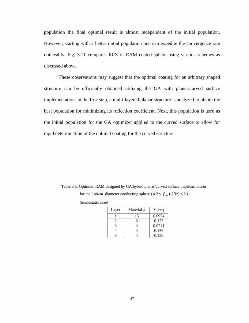
47
population the final optimal result is almost independent of the initial population.
However, starting with a better initial population one can expedite the convergence rate
noticeably. Fig. 3.11 compares RCS of RAM coated sphere using various schemes as
discussed above.
These observations may suggest that the optimal coating for an arbitrary shaped
structure can be efficiently obtained utilizing the GA with planer/curved surface
implementation. In the first step, a multi-layered planar structure is analyzed to obtain the
best population for minimizing its reflection coefficient. Next, this population is used as
the initial population for the GA optimizer applied to the curved surface to allow for
rapid determination of the optimal coating for the curved structure.
Table 3.5: Optimum RAM designed by GA hybrid planar/curved surface implementation
for the cm148 diameter conducting sphere ( 2)(2.0 ≤≤ GHzf opt ).
(monostatic case)
Layer Material # )(cmT 1 15 0.0954 2 6 0.177 3 4 0.0741 4 4 0.156 5 4 0.159

48
Fig. 3.11: Comparison of the RCS of the conducting sphere coated with the optimal spherical coating
(Table 3.4(a)), optimal planar coating (Table 3.2(a)), and optimal spherical coating using GA
hybrid planar/curved surface implementation (Table 3.5).
Fig. 3.12: Convergence curve of the GA hybrid planar/curved surface implementation compared to
the GA method for RCS reduction of the conducting sphere.
0.1 1.0 10.0frequency (GHz)
−60.0
−50.0
−40.0
−30.0
−20.0
−10.0
0.0
10.0
20.0
σ/λ2 (d
B)
Optimized spherical coating (GA)Optimized planar coating (GA)Optimized spherical coating (Hybrid GA)
0.0 20.0 40.0 60.0 80.0 100.0Generations (100 individual/generation)
5.0
10.0
15.0
20.0
25.0
30.0
35.0
RCS
Redu
ction
(dB)
GAGA Hybrid

49
3.5 Summary
In this chapter, a novel procedure for synthesizing RAM in a wide-band frequency range
for reducing RCS of curved targets is presented. Multi-layered planar, cylindrical, and
spherical canonical structures are analyzed using the vector wave solution of Maxwell’s
equations. Subsequently, the genetic algorithm optimization technique is integrated with
the modal solutions to obtain the optimal absorbing materials for RCS reduction. Since
the genetic algorithm produces the global solution without requiring much information
about the solution domain, it has been found to be a very effective method for obtaining
the optimal coating.
An in-depth study was performed to evaluate the potential usage of the optimal
planar coating as applied to the curved surfaces. It is observed that the optimal planar
coating can noticeably reduce RCS of curved structures. This observation was essential in
introducing a novel efficient GA implementation using as part of its initial generation the
best population obtained for the planar RAM design. These results suggest that the
optimal RAM for a surface with an arbitrary curvature may be efficiently determined by
applying the GA technique.
It is shown that for the structures studied in this paper by a proper composition of
absorbing materials, the monostatic RCS of the planar, cylindrical, and spherical
conducting structures is reduced about dB27 in the optimization frequency range of
GHz22.0 − . In the resonance region, the coating absorbs the energy of the incident wave
strongly; however, as one extends to the Rayleigh region the finite conductivity of some
of the RAM makes the coating act like a perfect conductor and the RCS cannot be

50
reduced as effectively as in the resonance region. Around the geometrical optics region,
the relative permittivity and permeability of the materials are decreased and the coating
cannot control the RCS of the structure effectively.
The bistatic RCS reduction of the coated conducting cylindrical and spherical
structures has also been investigated. It has been observed that, although the optimal
coating was achieved for reducing the monostatic RCS, due to the existence of loss, it has
also reduced the bistatic RCS in the lit region. In the deep shadow region no matter which
type of coating is used the scattered field is almost o180 out of phase with the incident
wave. Therefore, the optimal RAM only increases the size of the structure and cannot
reduce the bistatic RCS.
In addition, the effectiveness of the optimal planar coating in designing the
optimal RAM for the curved surfaces is investigated. It has been shown that the optimal
planar coating has almost the same effect as the optimal spherical coating in reducing the
monostatic RCS of spherical structures. Furthermore, the best population for the planar
coating is integrated as the initial population for an efficient GA technique to obtain the
optimal coating for the spherical structure. It has been shown that this implementation of
GA has a very fast convergence rate. This suggests that for the sake of the computational
time reduction, the optimal RAM for curved surfaces can be obtained using the GA
technique with the hybrid planar/curved strategy.

51
Chapter 4
Design Optimization of the Non-Uniform Luneburg and 2-Shell Lens Antennas
Searching for applicable antenna concepts for multi-beam scanning at millimeter and
microwave frequencies in mobile communication systems, remote sensing, and radio
astronomical, has renewed interest in multi-shell spherical lenses [6], [27]-[30]. These
types of lenses transform the feed’s spherical wave front into a plane wave [31]-[33].
Since the mathematical principle of the lens is based on geometrical optics, it can operate
over a broad band of frequencies. On the other hand, spherical symmetry of the lens
allows for multi-beam scanning by placing an array of feeds around the lens. These
attractive features of the multi-shell spherical lenses were the reason for their applications
as early as 1950 [34]-[37]. While both multi-shell spherical lenses and phased array
antennas can be used for beam scanning, the latter has a narrower frequency bandwidth.
An ideal Luneburg lens antenna consists of a dielectric sphere with varying
permittivity ranging from two at the center to one at the surface. In practice, the
Luneburg lens is constructed as a radially uniform multi-shell spherical lens that
efficiently focuses the feed energy. However, in order to achieve the typically demanded
high performance antenna characteristics, a large number of shells may be required. By

52
decreasing the number of shells the directivity is decreased, and substantially higher
levels of unwanted grating lobes are generated. This deficiency in the radiation
performance of the lens can be improved by designing a non-uniform lens to overcome
the grating lobe generations. The main question is how to choose the optimum layer
widths and dielectric constants for the shells, while minimizing the number of shells
necessary without introducing grating lobes.
This chapter focuses on the optimum synthesis of the non-uniform lens antennas
based on the genetic algorithm, in order to obtain the optimal material and thickness of
the spherical shells. Since it is desired to simultaneously control the achievable gain with
reduced grating lobe envelope, an adaptive cost function is used in the process of GA
optimization.
Various lens geometries including air gaps and feed offset from lens surface are
successfully optimized utilizing the vector wave solution of Maxwell’s equations
(Chapter 2) integrated with GA. Many useful engineering design guidelines have been
suggested for the optimum construction of the lens. The results have been satisfactory
and demonstrate the utility of the GA/adaptive-cost-function algorithm. Additionally,
radiation characteristics of a novel 2-shell lens antenna have been studied and its
performance is compared to the Luneburg lens. Furthermore, near field behaviors of the
optimized lens antennas are presented.

53
4.1 Modal Solution Integrated with GA/Adaptive-Cost-Function
The challenge in this section is to properly integrate the modal solution of Maxwell’s
equations for the multi-layered spherical structure with the GA/adaptive-cost-function in
order to present the optimal material and thickness of the spherical shells of the lens
antenna.
In the context of optimizing the radiation performance of the lens antenna with M
spherical shells, the objective or fitness function F is defined by
regionsidelobeMrMrr GfMinGTTTF )]()([),,...,,,,( 02211 θθβαεεε −⋅+⋅= (4.1)
where rjε and jT represent the material choice for each shell and its thickness,
respectively. )(θG is the gain pattern of the lens antenna in E-plane (note that a lens
antenna typically has similar E&H-plane patterns) and 0G is its maximum value. The
cost function F attains the maximum gain with low sidelobe levels, for an optimum
configuration. By a proper setting of parameters ,, βα and the sidelobe envelope function
)(θf , one can effectively control the gain and sidelobe levels.
In order to apply the GA method to the lens structure, the material and thickness
of each shell are represented in a binary code as
[ ][ ]tbmb Njjj
Njjjjjj tttmmmTML ...... 2121== (4.2)
where jM and jT are the finite sequences of binary bits representing the material and
thickness of thj spherical shell, respectively. The entire structure is subsequently
represented by the sequence MLLLG ...21= . To obtain the optimal material and thickness

54
with 3-digit resolution, each of the sequences jM or jT is included with 10 binary bits
10== tbmb NN . The size of the population is 100=popN . For each case, EM fields and
the cost function F are accurately computed. The evaluated cost function is suitably
incorporated into the GA method to present the optimal layered spherical lens antenna.
The optimization process has been depicted in Fig. 4.1. Note that in order to fix the outer
diameter of the lens a proper constraint has been applied on the total thickness of the
shells, as will discussed in Chapter 4.3.
Fig. 4.1: Genetic algorithm integrated with modal solution of Maxwell's equations for designing
optimum non-uniform lens antenna.
Analysis Technique
Modal Solution of Maxwell’s Equations
Optim
um N
on-Uniform
Lens w
ith Low N
umber of Shells
)( 21 aTTT M =+⋅⋅⋅++
z
x
y
Feed Antenna
12
Md
a
Genetic Algorithm
… … ……….. … … 11m 10
1m 11t
101t 1
Mm 10Mm 10
Mt
1M 1T MM MT……… 1Mt

55
4.2 Uniform Luneburg Lens Antenna and its Shortcomings
A Luneburg lens antenna transforms the point source radiation into the plane wave and
vice versa. An ideal Luneburg lens consists of a spherically symmetric dielectric sphere
with continuous varying permittivity from two at the center of inner core to the one at the
outer surface, i.e., ( )22 arr −=ε , where a is the radius of the sphere. In practice,
however, the Luneburg lens is constructed by a finite number of spherical shells,
retaining reasonable performance. Table 4.1 shows the material and thickness for a 5-
shell λ30 ( λ in free space) diameter uniform lens. Usually feed horns or open-ended
waveguides are used to illuminate the lens. In general, one could model the feed by its
equivalent dipole aperture field. In this paper, a typical horn antenna is modeled using an
end-fire antenna consisting of four infinitesimal dipoles, as shown in Figs. 4.2 and 4.3.
The end-fire antenna has cross polarization isolation around dB17 with about 7% spill-
over efficiency.
For a Luneburg lens antenna with fixed diameter, the radiation performance is
improved by increasing the number of shells, but the performance becomes saturated
with λ1≈ thickness for each shell. The radiation pattern of a 10-shell λ30 diameter lens
is shown in Fig. 4.4. As observed the gain is about dB73.37 (aperture efficiency
compared to the uniform aperture distribution is %)67=η . Note that due to the existence
of the periodic-like uniform shells, there appear some grating lobes in the pattern
occurring around o30≈θ . By reducing the number of shells the thickness of each shell is
increased and so the grating lobes are moved closer to the main beam, as shown for a 5-

56
shell lens (see Fig. 4.4). In this case the gain of the lens is decreased to dB46.36
( %)50=η and the grating lobes occur closer to the main beam, around o17≈θ . Note
that the location of the grating lobes for the periodic-like uniform Luneburg lens can be
estimated from the simple formula )(sin 1 Tλθ −= (T is the thickness of the spherical
shell), which gives o81.41=θ and o47.19=θ for the 10-shell and 5-shell lenses,
respectively.
Position of the feed antenna is the other important aspect in designing the
Luneburg lens antenna. From the geometrical optic point of view when the phase center
of the feed is on the surface, the lens antenna focuses the feed’s energy at the infinity.
However, in practice this condition may not be fulfilled and the phase correction of the
lens antenna becomes worse. The radiation pattern of a 5-shell λ30 diameter lens when
the feed is λ5.0 away the surface of the lens is shown in Fig. 4.4. One observes that the
dislocation of the feed degrades the lens performance by broadening the beam and
dropping the gain of the lens to about dB31.35 ( %)38=η .
Air-gaps between spherical shells of the Luneburg lens antenna may be
unavoidable in the process of constructing the lens. This air gap affects the performance
of the lens as illustrated in Fig. 4.4. The radiation pattern of the 5-shell λ30 diameter
lens with λ05.0 air gap shows the effect of the air gap by decreasing the gain of the lens
to about dB46.35 ( %)40=η .
From these plots, it is demonstrated that a 10-shell λ30 lens antenna has the
superior performance. Although, a 5-shell lens antenna with less number of spherical

57
shells has the easier construction, however, due to the larger thickness of each shell the
grating lobes occur closer to the main beam degrading the performance of the antenna.
An optimized non-uniform 5-shell lens antenna is introduced in the next section to
noticeably improve the radiation characteristics of the uniform lens including gain, side
lobe level, and grating lobes.
Table 4.1: Design parameters of a 5-shell λ30 diameter uniform
Luneburg lens antenna.
Shell rε λT
1 1.180 3 2 1.500 3 3 1.740 3 4 1.900 3 5 1.980 3
Fig. 4.2: 5-shell λ30 diameter Luneburg lens antenna. An end-fire antenna consisting
of four infinitesimal dipoles models the actual feed.
z
λ30
λ25.0
λ5.0
y
x
o0o90
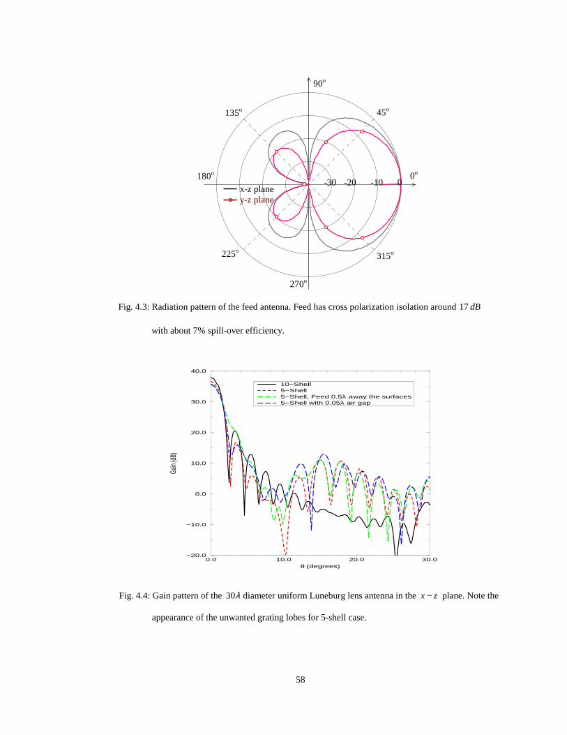
58
Fig. 4.3: Radiation pattern of the feed antenna. Feed has cross polarization isolation around dB17
with about 7% spill-over efficiency.
Fig. 4.4: Gain pattern of the λ30 diameter uniform Luneburg lens antenna in the zx − plane. Note the
appearance of the unwanted grating lobes for 5-shell case.
x-z plane y-z plane
0-10-20-30 0o
45o
90o
135o
180o
225o
270o
315o
0.0 10.0 20.0 30.0θ (degrees)
−20.0
−10.0
0.0
10.0
20.0
30.0
40.0
Gain
(dB)
10−Shell5−Shell5−Shell, Feed 0.5λ away the surfaces5−Shell with 0.05λ air gap

59
4.3 Non-Uniform Luneburg Lens Antenna
This section focuses on the key design aspects of a non-uniform Luneburg lens antenna
using the genetic algorithm. The goal is to determine the permittivity and thickness of
each spherical shell for a 5-shell λ30 diameter lens antenna such that the maximum gain
is achieved. However, besides maximizing the gain, the level of sidelobes should remain
low. The challenge then is to investigate the tradeoffs between these conflicting
objectives.
4.3.1 GA Implementation
In this study, the number of shells is 5=M , and rjε is allowed to change between 1.0 to
2.0. In the procedure of the optimization, the total diameter of the lens antenna is kept
fixed at λ30 . In other words the optimum thickness of the spherical shells should satisfy
the following equation
⋅=+⋅⋅⋅++ λ15521 TTT (4.3)
For imposing this condition, the thickness of each shell can be allowed to change
arbitrarily between 0 to λ15 , and then the appropriate thickness is selected based on a
scaling approach. This means that the appropriate thickness of each shell is obtained
using the scaling coefficient GAlens DD=ζ . lensD is the actual diameter of the lens, and
GAD is the determined diameter from the GA procedure. However, this method is time
consuming.

60
As mentioned earlier, the ideal Luneburg lens has a dielectric constant
( )22 arr −=ε with the slope 22 ar−=ν . It reveals that, the inhomogeneous
permittivity of the lens has the larger slope variation near the surface of the lens
compared to the inside of the lens. Therefore, in order to design a high performance
multi-shell lens antenna, the larger number of spherical shells has to be used near the
surface of the lens, which may be explained as follow.
Each spherical shell can be considered as a focusing device where by choosing
the optimal material the phase error is reduced and the waves are focused properly. The
quality of focusing is inversely proportional to the projected area of the spherical shells,
and to obtain a good design the inner shells should have a bigger thickness compared to
the outer shells; and then a larger number of layers is necessary near the surface of the
lens compared to the inside of the lens. Therefore, to achieve a fast optimum design, the
following constraint on the thickness of spherical shells is imposed:
,40,50,9.20,9.20 4321 λλλλ ≤≤≤≤≤≤≤≤ TTTT (4.4)
whereas the inner thickness, 5T , is obtained based on the Eq. (4.3). Imposing constraints
such as Eq. (4.4) implicitly allows a bigger range for the inner shells in the GA process
and fulfills the aforementioned requirements.
4.3.2 Non-Uniform Lens with Improved Gain
For achieving the maximum gain the parameters α and β in Eq. (4.1) are chosen 1 and
0, respectively. Table 4.2(a) and Fig. 4.5 show the design parameters and the gain pattern
of a 5-shell non-uniform lens. As observed, a thicker core compared to the uniform

61
design is obtained which helps the increment in the gain of the lens antenna by dB1 to
dBG 47.370 = ( %)63=η . Additionally, the grating lobe is decreased about dB5.6 with
respect to the uniform design.
4.3.3 High Gain/Low Sidelobe Non-Uniform Lens
Utilizing an appropriate cost function into the GA method one can design a non-uniform
lens antenna with high gain and remarkably reduced grating lobes. In this manner, the
parameter β and envelope function )(θf are properly incorporated into the Eq. (4.1) to
control the sidelobes of the lens. As noted earlier, the λ30 10-shell uniform Luneburg
lens antenna has the acceptable monotonically decaying sidelobe variations. Therefore,
the function f is taken as the envelope of these sidelobes in the following form (as
shown in Fig. 4.6)
⋅−= )()8.5log(3812)( dBf ooθθ (4.5)
In this case, a useful design is obtained by choosing ,1=α and 5.0=β . The goal
is to achieve the maximum gain while the sidelobes level is kept low, similar to a 10-shell
lens. In order to create an adaptive cost function in the process of the GA optimization,
the objective function F is taken as the antenna gain (i.e., β = 0) in the first 20
generations. Next, the effect of both high gain and low sidelobes level are jointly used in
the process of the optimization. This helps the optimization method to keep the antenna
gain in a high level while decreasing the sidelobe levels.

62
The results are presented in Table 4.2(b) and Fig. 4.7. Note that the function f
was chosen to control the sidelobe levels in the angular range oo 255.2 ≤≤ θ at 50
points. To reduce the grating lobes, in general, the spherical shells should be very thin,
which needs a large number of shells. However, in this study the lens antenna has only 5
layers and as indicated in Table 4.2(b), the GA optimizer makes the intermediate shell
thicker to allow a smaller thickness for the neighboring layers. Fig. 4.7 shows that the
gain is about dB94.35 ( %)44=η and the grating lobes are decreased about dB12 with
respect to the uniform design. Although, in this design the gain is dropped by dB5.1
compared to the previous case )0,1( == βα , but the grating lobes are noticeably
suppressed under the envelope function f .
The effectiveness of this adaptive optimization technique is shown in Fig. 4.8 by
varying α and β in Eq. (4.1). It is observed that simultaneous application of α and β
in the cost function provides the improved result. Fig. 4.9 shows a typical convergence
curve of the GA method for three different sets of α and β . For 1=α and 0=β , the
gain converges to the optimum value rapidly. However, for 0=β the grating lobe cannot
be controlled. When the optimization parameters 0=α and 1=β , there is no constraint
on the directivity and the antenna gain is decreased significantly, as observed in Fig. 4.9.
Therefore, 1=α and 5.0=β values have provided an efficient adaptive optimization by
controlling the gain and grating lobe of the lens antenna. Note that a Pareto GA's [20]
may be used to further refine the design by creating a set of optimized solutions.

63
4.3.4 Optimal Non-Uniform Lens with Feed Offset and Air Gap
The radiation pattern of a λ30 lens antenna when the phase center of the feed has been
moved λ5.0 away from the surface, for two different optimization sets 0,1 == βα and
5.0,1 == βα has been plotted in Fig. 4.10. The design parameters of the lens have been
shown in Table 4.3. It is observed that the pattern is improved with respect to the uniform
design by correcting the phase center of the feed using the non-uniform lens design. In
the first case, the gain is increased to about dB73.36 ( %)53=η and in the second case,
the grating lobe is also controlled using the adaptive cost function.
As mentioned earlier, the existence of the air gap between spherical shells may be
unavoidable in the constructing process of the Luneburg lens antenna. The optimized
material and thickness for a 5-shell lens with λ05.0 air gap, using cost function F with
two different optimization parameters 0,1 == βα and 5.0,1 == βα are presented in
Table 4.4. Fig. 4.11 shows the radiation pattern of the optimized lens. The results show
the validity of the GA method for designing such a lens antenna with air gap.
The other interesting aspect of this optimization technique is to design a practical
lens antenna with λ05.0 air gap and feed λ5.0 away from its surface. The radiation
pattern for the uniform Luneburg lens is shown in Fig. 4.12 and as observed the lens can
not focus the feed energy as well as before and the performance of the lens is decreased
significantly. The characteristics of the lens are improved by designing a non-uniform
lens as shown in Table 4.5, for two different optimization cases 0,1 == βα and
5.0,1 == βα . The radiation pattern is plotted in Fig. 4.12. It is observed that the
directivity of the optimum design for 0,1 == βα is about dB48.36 ( %)50=η and the

64
grating lobes are decreased about dB2.5 with respect to the uniform design. Using the
adaptive cost function ( 5.0,1 == βα ) the grating lobes are better controlled as shown in
Fig. 4.12.
Therefore, the radiation performance of the uniform Luneburg lens antenna is
considerably improved by designing the non-uniform lens using the adaptive GA method.
The antenna gain is increased and the grating lobes are suppressed noticeably. The
sensitivity of the optimum design based on the tolerance in the dielectric constant rε is
also studied in this work. The radiation performance of the non-uniform optimized lens
( 0,1 == βα ), using 3-digit, 2-digit, and 1-digit accuracy in rε , is plotted in Fig. 4.13. It
is observed that for a high performance lens design a dielectric constant with at least 2-
digit accuracy should be used. Co-polarized and cross polarized fields of the optimized
lens antenna are also presented in Fig. 4.14. It is noted that the non-uniform lens antenna
has a cross polarization isolation of dB23 . Clearly, lower cross polarization can be
achieved using a more symmetric feed patterns.

65
Table 4.2: Design parameters of a 5-shell λ30 diameter non-uniform Luneburg lens antenna,
(a) 0,1 == βα , (b) 5.0,1 == βα .
(a) Shell rε λT
1 1.203 2.798 2 1.469 2.047 3 1.642 2.030 4 1.797 2.464 5 1.942 5.661
(b) Shell rε λT
1 1.075 1.819 2 1.191 1.232 3 1.725 3.710 4 1.815 1.615 5 1.948 6.624
Table 4.3: Design parameters of a 5-shell λ30 diameter non-uniform Luneburg lens antenna. Feed
is positioned λ5.0 away the surface of the lens, (a) 0,1 == βα , (b) 5.0,1 == βα .
(a) Shell rε λT
1 1.325 1.870 2 1.190 1.478 3 1.556 2.917 4 1.739 2.689 5 1.899 6.046
(b) Shell
rε λT
1 1.118 1.865 2 1.217 1.331 3 1.621 3.100 4 1.734 1.816 5 1.877 6.888
Table 4.4: Design parameters of a 5-shell λ30 diameter non-uniform Luneburg lens antenna with
λ05.0 air gap, (a) 0,1 == βα , (b) 5.0,1 == βα .
(a) Shell rε λT
1 1.338 0.519 2 1.125 2.611 3 1.537 2.768 4 1.713 2.568 5 1.878 6.334
(b) Shell rε λT
1 1.050 1.863 2 1.189 1.400 3 1.601 2.721 4 1.750 2.943 5 1.896 5.873
Table 4.5: Design parameters of a 5-shell λ30 diameter non-uniform Luneburg lens antenna with
λ05.0 air gap. Feed is positioned λ5.0 away the surface of the lens, (a) 0,1 == βα ,
(b) 5.0,1 == βα .
(a) Shell rε λT
1 1.080 0.915 2 1.195 2.450 3 1.599 2.895 4 1.736 2.394 5 1.883 6.146
(b) Shell rε λT
1 1.081 2.094 2 1.220 1.319 3 1.616 2.463 4 1.708 3.066 5 1.886 5.858

66
Fig. 4.5: Gain pattern of the 5-shell λ30 diameter uniform and non-uniform optimized lens antenna
in the zx − plane. ( 0,1 == βα )
Fig. 4.6: Gain pattern of the 10-shell λ30 diameter uniform Luneburg lens antenna with its sidelobe
envelope function ( ) )(8.5log3812)( dBf ooθθ −= , in the zx − plane.
0.0 10.0 20.0 30.0θ (degrees)
−20.0
−10.0
0.0
10.0
20.0
30.0
40.0
Gain
(dB)
Uniform designGA (α=1, β=0)
0.0 10.0 20.0 30.0θ (degrees)
−20.0
−10.0
0.0
10.0
20.0
30.0
40.0
Gain
(dB)
Uniform design, 10−ShellEnvelop function

67
Fig. 4.7: Comparison between 10-shell and 5-shell uniform design with the 5-shell non-uniform
optimized lens in the zx − plane. (adaptive cost function: 5.0,1 == βα )
Fig. 4.8: Gain pattern of the 5-shell non-uniform optimized lens using different optimization
parameters α and β .
0.0 10.0 20.0 30.0θ (degrees)
−20.0
−10.0
0.0
10.0
20.0
30.0
40.0
Gain
(dB)
Uniform design, 10−ShellUniform design, 5−ShellGA (α=1, β=0.5)
0.0 10.0 20.0 30.0θ (degrees)
−20.0
−10.0
0.0
10.0
20.0
30.0
40.0
Gain
(dB)
α=1, β=0.α=1, β=0.5α=0, β=1.

68
Fig. 4.9: Convergence curve of the GA method for the 5-shell non-uniform optimized lens using
different optimization parameters α and β .
Fig. 4.10: Gain pattern of the 5-shell λ30 diameter non-uniform optimized lens antenna in the zx −
plane. Feed is positioned λ5.0 away the surface of the lens. ( 0,1 == βα and 5.0,1 == βα )
0.0 10.0 20.0 30.0θ (degrees)
−20.0
−10.0
0.0
10.0
20.0
30.0
40.0
Gain
(dB)
Uniform designGA (α=1, β=0)GA (α=1, β=0.5)
0.0 20.0 40.0 60.0 80.0 100.0Generations (100 individual/generation)
20.0
25.0
30.0
35.0
40.0
Gain
(dB)
α=1, β=0α=1, β=0.5α=0, β=1
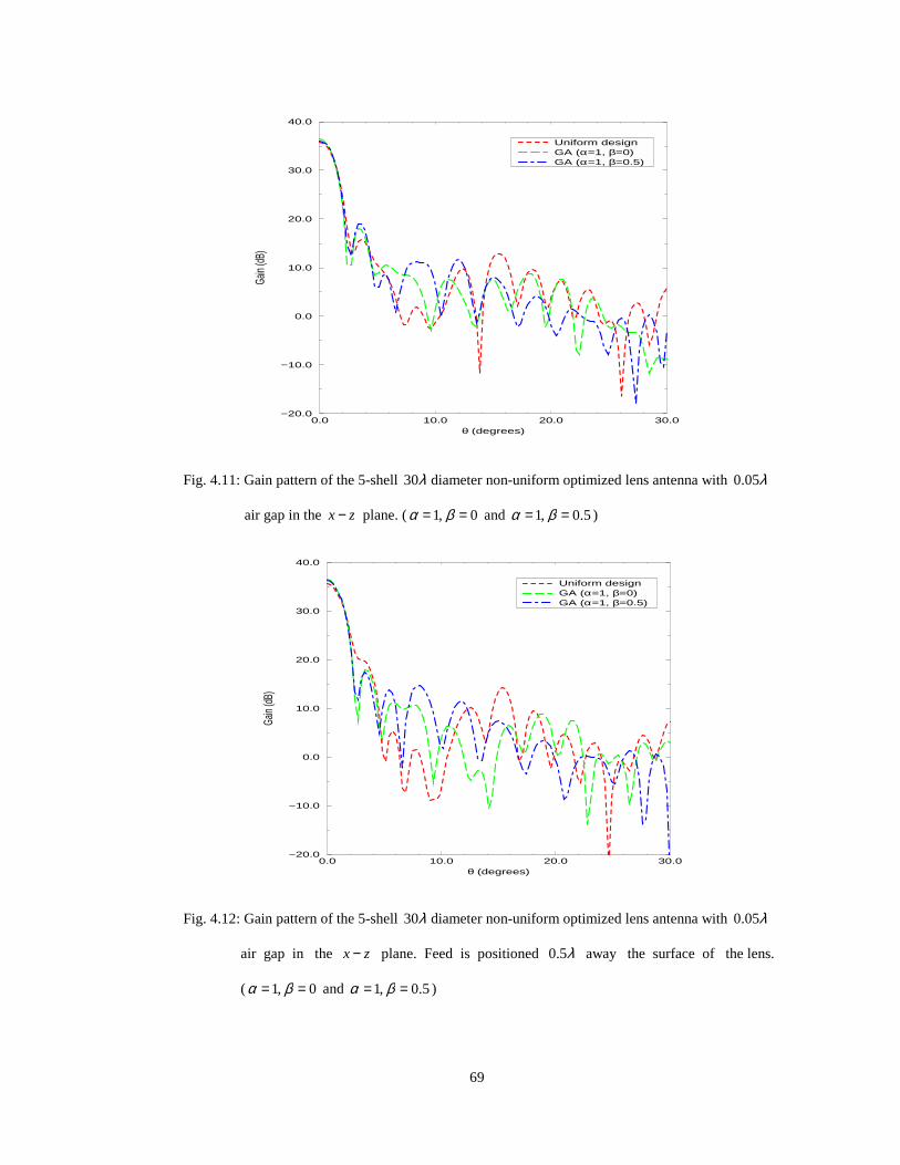
69
Fig. 4.11: Gain pattern of the 5-shell λ30 diameter non-uniform optimized lens antenna with λ05.0
air gap in the zx − plane. ( 0,1 == βα and 5.0,1 == βα )
Fig. 4.12: Gain pattern of the 5-shell λ30 diameter non-uniform optimized lens antenna with λ05.0
air gap in the zx − plane. Feed is positioned λ5.0 away the surface of the lens.
( 0,1 == βα and 5.0,1 == βα )
0.0 10.0 20.0 30.0θ (degrees)
−20.0
−10.0
0.0
10.0
20.0
30.0
40.0
Gain
(dB)
Uniform designGA (α=1, β=0)GA (α=1, β=0.5)
0.0 10.0 20.0 30.0θ (degrees)
−20.0
−10.0
0.0
10.0
20.0
30.0
40.0
Gain
(dB)
Uniform designGA (α=1, β=0)GA (α=1, β=0.5)

70
Fig. 4.13: Gain pattern of the 5-shell λ30 diameter non-uniform optimized lens antenna using 3-digit,
2-digit, and 1-digit accuracy in the dielectric constant rε , in the zx − plane. ( 0,1 == βα )
Fig. 4.14: Co-polarization and cross polarization of the 5-shell λ30 diameter non-uniform optimized
lens antenna in the ,45,0 oo == φφ and o90=φ planes. ( 0,1 == βα )
0.0 10.0 20.0 30.0θ (degrees)
−20.0
−10.0
0.0
10.0
20.0
30.0
40.0
Gain
(dB)
3 Digits2 Digits1 Digit
−30.0 −20.0 −10.0 0.0 10.0 20.0 30.0θ (degrees)
−20.0
−10.0
0.0
10.0
20.0
30.0
40.0
Gain
(dB)
φ=0 (co−pol)φ=0 (x−pol)φ=45 (co−pol)φ=45 (x−pol)φ=90 (co−pol)φ=90 (x−pol)

71
4.4 2-Shell Lens Antenna
Geometrical optic theory predicts that a relatively high dielectric constant lens antenna
can also collimate the feed energy in the front of the lens. A 2-shell lens antenna,
proposed by T. L. Ap-Rhys [38], has the potential to satisfy the design requirements
insofar as maximum gain and low side lobe level is concerned. This idea is supported by
using the ray optic theory [31], [32], as illustrated in Fig. 4.15. Optical rays crossing the
surface of the lens antenna at an angle iθ , can exit parallel to the axis of the lens by
choosing suitable values for the dielectric constant of the shells. The core of the lens
focuses the optical rays and the outer shell is a matching layer.
In this section, the GA technique is successfully applied to the design of 2-shell
lens antenna, in order to obtain the optimal material and thickness of the core and
matching layer. Optimal characteristics of the 2-shell λ30 diameter lens for two different
optimization parameters 0,1 == βα and 5.0,1 == βα are obtained in Table 4.6, and as
observed the matching layer is about a quarter wavelength. In this study, the dielectric
constant rjε is allowed to change between 1.0-5.0, and the thickness of the outer shell is
changed between 0 to λ2 . The radiation pattern of the optimized 2-shell λ30 lens is
plotted in Fig. 4.16. For optimization parameters 0,1 == βα , the directivity is about
dB48.37 ( %)63=η and additionally the envelope of sidelobes decays very well
compared to the Luneburg lens antenna. However, the first sidelobe is increased, as
observed from this plot. In this case, there are no grating lobes and then almost the same

72
result for the adaptive optimization with 5.0,1 == βα is achieved, as shown in Fig.
4.16.
In order to show the effect of the matching layer in reducing the back-scattered
waves, the radiation pattern of a homogeneous lens antenna with the proper dielectric
constant 315.3=rε (core without matching layer) is obtained in Fig. 4.16. As obtained,
compared to the 2-shell lens antenna, the gain is dropped by about dB24.0 and the back-
scattered waves are noticeably increased.
The manufacturing procedure of this type of lens is easier than for the Luneburg
lens antenna. The inner core can be constructed from the Quartz-like material with
dielectric constant 4.32 =rε ; and for the matching shell, Teflon with 1.21 =rε may be
suitable. However, application of higher dielectric constant material could make these
lenses heavier than the Luneburg lens.
The frequency dependence of the 2-shell lens antenna is studied in Table 4.7, and
compared with the 5-shell non-uniform Luneburg lens. In each case, the same radiation
characteristic for the feed antenna is used. As determined, the 2-shell and 5-shell lens
antennas have the %63 efficiency at center frequency 0f (lenses have been designed at
this frequency). At %10 below the center frequency 0f , we obtain the same efficiency;
however, the efficiency at %10 above the center frequency is decreased %4 and %5 for
the 2-shell and 5-shell lens antennas, respectively. These lenses have lower efficiency at
07.0 f and 03.1 f ( %30± coverage of the frequency bandwidth), as shown in Table 4.7.

73
The larger frequency bandwidth could be expected for the lens antenna with more
number of spherical shells.
Fig. 4.15: Geometrical optic theory applied to a relatively high dielectric 2-shell lens antenna.
Table 4.7: Frequency dependency of the 2-shell and 5-shell optimized lens antennas. ( 0,1 == βα )
Frequency 07.0 f 09.0 f 0f 01.1 f 03.1 f
Efficiency of 2-shell lens %53 %63 %63 %59 %46 Efficiency of 5-shell lens %45 %63 %63 %58 %45
Aperture Plane
Boresight 2ε
F
tθ
iθ
1ε
Table 4.6: Design parameters of a 2-shell lens antenna, (a) 0,1 == βα , (b) 5.0,1 == βα .
(a) (b) Shell rε λT
1 2.224 0.218 2 3.315 14.782
Shell rε λT 1 1.868 0.209 2 3.287 14.791

74
Fig. 4.16: Gain patterns of the λ30 diameter optimized 2-shell and homogeneous ( 315.3=rε ) lens
antennas in the zx − plane. ( 0,1 == βα and 5.0,1 == βα )
4.5 Near Field Characteristics of the Lens Antenna
The focusing behavior of the lens antenna can be clearly illustrated by investigating the
near field pattern of the lens. However the near field computation of the λ30 diameter
spherical lens antenna is time consuming. To reduce the computational effort necessary
to calculate the near field of the spherical lens, it is often sufficient to utilize a cylindrical
lens instead of the spherical lens.
In the cylindrical structure the electromagnetic fields can be represented in both
TMz and TEz polarizations. In this study, the TEz polarization is considered where the
component of the electric field parallel to the axis of the cylinder is equal to zero (E-
0.0 10.0 20.0 30.0θ (degrees)
−20.0
−10.0
0.0
10.0
20.0
30.0
40.0
Gain
(dB)
2−Shell, GA (α=1, β=0)2−Shell, GA (α=1, β=0.5)Homogeneous lens

75
plane). This is consistent with the electric field in zx − plane for the spherical lens
antenna.
To validate the possibility of investigating the performance of the spherical lens
utilizing the cylindrical lens, the radiation pattern of a 5-shell λ30 diameter spherical
lens with the material and thickness determined from the optimization of a cylindrical
structure (Table 4.8) is presented in Fig. 4.17. As observed the gain is about dB21.36
demonstrating that the optimal layers have almost the similar effects in both cylindrical
and spherical structures for focusing the feed energy. This may suggest that the near field
phenomenon of the spherical lens can also be effectively visualized using a cylindrical
structure.
4.5.1 Focusing Behavior of the Luneburg Lens
Fig. 4.18 shows the computed near field pattern of the 5-shell λ30 diameter cylindrical
Luneburg lens antenna using the same material and thickness for the optimized spherical
lens for maximum gain (Table 4.2(a)). Note that the input radiated power is normalized to
W0.1 . As illustrated, the optimal lens antenna successfully collimates the rays from the
feed and generates an almost plane wave on the exiting aperture.
4.5.2 Focusing Behaviors of the Constant and 2-Shell Lenses
Near field characteristics of the λ30 constant cylindrical lens antenna with dielectric
constant 315.3=rε is shown in Fig. 4.19. It is observed that the most part of the feed
energy is drawn into the lens antenna. Additionally, some of the rays penetrate inside the

76
lens close to the critical angle, and they are almost totally reflected from the surface of
the lens. Therefore, many paths through the lens are observed where they add
constructively. Due to this effect, a glory region [39] with thickness about λ6 is
observed in the lens antenna.
As mentioned earlier, the performance of the constant lens antenna can be further
improved by designing a 2-shell lens antenna (Table 4.6(a)). Fig. 4.20 shows the near
field performance of the 2-shell cylindrical lens antenna. As illustrated in this figure, the
outer shell or matching layer reduces the back-scattered waves and the lens antenna
focuses the source radiation strongly. Note that the thickness of the matching layer is
λ218.0=T where again due to the totally reflected waves a glory region with thickness
about λ6 is produced. The electric field in this orbiting area is very strong representing a
hot glory region. It means that in this case there are more in-phase rays in the glory
region with respect to the constant lens antenna.
The aperture field of the 2-shell lens antenna is more uniform (i.e. less tapered)
compared to the 5-shell non-uniform lens resulting in a higher sidelobe level. These near
field characteristics may be used to better understand the radiation performance of the
lens and seek for a better design.

77
Table 4.8: Design parameters of a 5-shell λ30 diameter non-uniform cylindrical
Luneburg lens antenna. ( 0,1 == βα )
Shell rε λT
1 1.217 3.451 2 1.476 2.129 3 1.670 2.523 4 1.824 2.577 5 1.933 4.320
Fig. 4.17: Gain pattern of the 5-shell λ30 diameter non-uniform spherical lens antenna in the zx −
plane using the optimal material and thickness determined from the optimization of the
cylindrical lens (Table 4.8). ( 0,1 == βα )
0.0 10.0 20.0 30.0θ (degrees)
−20.0
−10.0
0.0
10.0
20.0
30.0
40.0
Gain
(dB)

78
Fig. 4.18: Near field contour plot of the 5-shell λ30 diameter non-uniform cylindrical Luneburg lens
antenna. (material and thickness are the same as the optimized 5-shell spherical lens
(Table 4.2(a)))
Fig. 4.19: Near field contour plot of the λ30 diameter constant cylindrical lens antenna. (material and
thickness are the same as the constant spherical lens, ( 315.3=rε ))
-25.0 -20.0 -15.0 -10.0 -5.0 0.0 5.0 10.0 15.0 20.0 25.0
25.0
20.0
15.0
10.0
5.0
0.0
-5.0
-10.0
-15.0
-20.0
-25.0
x (wavelength)
y (w
avel
engt
h)
0.0 10.0 20.0 30.0 40.0 50.0 60.0 70.0
E (dB)
-25.0 -20.0 -15.0 -10.0 -5.0 0.0 5.0 10.0 15.0 20.0 25.0
25.0
20.0
15.0
10.0
5.0
0.0
-5.0
-10.0
-15.0
-20.0
-25.0
x (wavelength)
y (w
avel
engt
h)
0.0 10.0 20.0 30.0 40.0 50.0 60.0 70.0
E (dB)

79
Fig. 4.20: Near field contour plot of the 2-shell λ30 diameter cylindrical lens antenna. (material and
thickness are the same as the optimized 2-shell spherical lens (Table 4.6(a)))
4.6 Summary
In this work, non-uniform spherical lens antennas are synthesized using genetic
algorithms. The multi-shell lens antenna is analyzed using the vector wave solution of
Maxwell’s equations. The GA/adaptive-cost-function is applied to obtain the optimal
material and thickness of the spherical shells for designing the optimal lens antenna with
high performance radiation characteristics.
It is demonstrated that the radiation performance of the uniform Luneburg lens
antenna with low number of shells is noticeably improved by designing a non-uniform
lens; shells of varying widths and dielectric constants. By choosing an appropriate cost
function, the gain of the 5-shell λ30 lens is increased about dB1 , and also its grating
-25.0 -20.0 -15.0 -10.0 -5.0 0.0 5.0 10.0 15.0 20.0 25.0
25.0
20.0
15.0
10.0
5.0
0.0
-5.0
-10.0
-15.0
-20.0
-25.0
x (wavelength)
y (w
avel
engt
h)
0.0 10.0 20.0 30.0 40.0 50.0 60.0 70.0
E (dB)

80
lobes decreased by dB5.6 with respect to the uniform design. Using the GA optimizer
with adaptive cost function one can effectively control both directivity and sidelobe of
the lens, as illustrated in a non-uniform lens design with improved gain ad remarkably
suppressed grating lobes. Additionally, even when the feed is not on the surface or an air
gap exists between the shells, the GA method can optimize the lens parameters
successfully.
Sensitivity of the optimized lens antenna based on the accurate knowledge of the
dielectric constant rε is also studied in this chapter. It is observed that for a high
performance lens design, a dielectric constant with at least 2-digit accuracy should be
used. Furthermore, cross polarization of the non-uniform lens antenna is computed and is
shown that in this case there is about dB23 isolation. This isolation level can be further
improved by using a feed with more symmetric patterns.
Design optimization of a novel 2-shell lens antenna consisting of a core coated
with a matching layer is also presented. It is obtained that the lens has the potential to
present a radiation performance with high gain and low sidelobe level variations. Also, it
is shown that the 2-shell and 5-shell lens antennas have almost the similar bandwidth
characteristics for the design cases studied in this paper.
The near field characteristics of the Luneburg, constant, and 2-shell lens antennas
are also investigated. It is illustrated that the optimal lens antennas properly transfer the
spherical feed radiation to the plane wave. The near field behavior of the lens can be used
to better understand the performance of the antenna resulting in design of lens antenna
with higher radiation characteristics.

81
Although this chapter focuses on the optimization over a continuous parameter
set, however, as obtained in the previous chapter, the GA method is also capable to apply
on the discrete structural parameters. This means that by using the optimization
technique, the best material and thickness for the lens can be picked up among a finite set
of materials in a database. In summary, the methodologies developed in this work will
allow efficient design of multi-layered lens antennas based on the specifications of the
desired application.

82
Chapter 5
Broadband Characterization of Complex EBG Structures
Periodic structures are abundant in nature and they have fascinated artists and scientists
alike. When they interact with electromagnetic waves amazing features result. In particular,
characteristics such as frequency stop-bands, pass-bands and band-gaps could be identified.
Surveying the literature, one observes that various terminology have been used depending
on the domain of the applications. These applications are seen in filter designs, gratings,
Frequency Selective Surfaces (FSS), Photonic Band-Gaps (PBG) materials, etc [10]-[12].
In this dissertation these structures are classified under the broad terminology of
“Electromagnetic Band-Gaps (EBG)” [7]. Generally speaking, EBG structures are 3-D
periodic objects that prevent the propagation of the electromagnetic waves in a specified
band of frequency for all angles of arrival and for all polarization states. However, in
practice, it is very hard to obtain such complete band-gap structures and partial band-gaps
are achieved. For example, filters typically cover the scalar situation and single angle of
arrival. FSS typically cover limited angles of arrival and respond differently to polarization
states. PBG typically cover in-plane angles of arrival and also sensitive to polarization

83
states. FSS terminology has been widely used in the microwave community while PBG
terminology has been widely applied in the optical community.
Periodic structures are often analyzed using frequency domain integral equations
and Method of Moment (MoM) solutions [10], [40]. Because of the required evaluation
of periodic Green’s function, and the frequent desire to repeat the analysis at multiple
frequencies, these approaches can become computationally intensive. Finite Difference
Time Domain (FDTD) technique is an alternative approach to efficiently present the
broadband characteristics of the periodic structures.
The main objective of this chapter is to develop an efficient and powerful
computational engine utilizing FDTD technique to characterize and understand the
unique propagation performances of the periodic EBG structures composed of complex
scatterers of dielectrics and conductors of arbitrary shapes. There have been several
methods proposed to implement the periodic boundary conditions in FDTD [9]. The
sin/cos and split-field approaches are the most capable techniques in analyzing periodic
structures. Basic mathematical concepts of these methods are developed in [9]. The focus
in this chapter is to derive and organize the formulations and detail some of the steps,
which one needs to effectively apply the FDTD technique.
5.1 Analysis Technique
In this section, the development of the FDTD technique with Periodic Boundary
Condition/Perfectly Matched Layer (PBC/PML) in analyzing periodic structures at
oblique incidence is presented. Taking advantage of the broadband analysis of the FDTD

84
approach provides great efficiency and accuracy when the structure is characterized to
demonstrate its frequency response. The Prony’s extrapolation scheme is also
incorporated to increase the efficiency of the computational engine. The main parts of
this computational engine as illustrated in Fig. 5.1 are discussed in the following sections.

85
Fig. 5.1: Powerful and efficient computational engine utilizing FDTD technique in the characterization
of complex periodic EBG structures.
• Yee Algorithm • Total Field/Scattered Field • Periodic Boundary Conditions (PBC) • Perfectly Matched Layer (PML) Absorbing
Boundary Conditions (ABC) • Prony’s Method
x
y
z
kjixH ,,,
kjizH ,,,
kjiyH ,,,kjizE ,,,
kjizE ,,1, −
1,,, −kjixE
kjixE ,1,, −
kjizE ,1,, −
kjiyE ,,,
1,,, −kjiyE
kjiyE ,,1, −
kjixE ,,,
Yee Algorithm
sE
iE
sE
Structure Lattice Truncation
Total Field
Scattered Field
Virtual Connecting Surface
Total Field/Scattered Field
PML ( 0,0,,,, 2211∗∗yyxx σσσσ )
PML (*
2222 ,,,,0,0 zzyy σσσσ ∗)
x
y
z
PML (*2222 ,,0,0,, zzxx σσσσ ∗)
PML ( 0,0,0,0,, 22∗xx σσ )
PML (*
222211 ,,,,, zzyyxx σσσσσσ ∗∗)
PML (*22 ,,0,0,0,0 zz σσ )
PML ( 0,0,,,0,0 22∗yy σσ )
PML (*2211 ,,0,0,, zzxx σσσσ ∗
)
PML (*
222222 ,,,,, zzyyxx σσσσσσ ∗∗)
PML ( 0,0,,,, 2222∗∗yyxx σσσσ )
PML ABC PBC
• Sin/Cos • Split-Field
z
x
y
PML
PBC
PBC
Prony’s Method
∑=
=M
m
nmmn zad
1
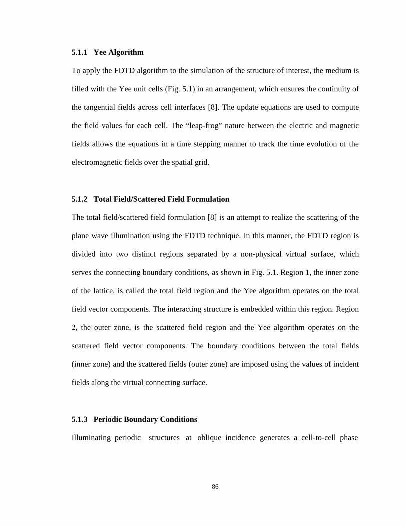
86
5.1.1 Yee Algorithm
To apply the FDTD algorithm to the simulation of the structure of interest, the medium is
filled with the Yee unit cells (Fig. 5.1) in an arrangement, which ensures the continuity of
the tangential fields across cell interfaces [8]. The update equations are used to compute
the field values for each cell. The “leap-frog” nature between the electric and magnetic
fields allows the equations in a time stepping manner to track the time evolution of the
electromagnetic fields over the spatial grid.
5.1.2 Total Field/Scattered Field Formulation
The total field/scattered field formulation [8] is an attempt to realize the scattering of the
plane wave illumination using the FDTD technique. In this manner, the FDTD region is
divided into two distinct regions separated by a non-physical virtual surface, which
serves the connecting boundary conditions, as shown in Fig. 5.1. Region 1, the inner zone
of the lattice, is called the total field region and the Yee algorithm operates on the total
field vector components. The interacting structure is embedded within this region. Region
2, the outer zone, is the scattered field region and the Yee algorithm operates on the
scattered field vector components. The boundary conditions between the total fields
(inner zone) and the scattered fields (outer zone) are imposed using the values of incident
fields along the virtual connecting surface.
5.1.3 Periodic Boundary Conditions
Illuminating periodic structures at oblique incidence generates a cell-to-cell phase

87
variation between corresponding points in different unit cells, which causes the time
domain implementation to become challengeable. In this work, to achieve a powerful
computational tool, the Floquet type phase shift periodic boundary condition is
incorporated based on two recently introduced approaches as: (a) doubly excited
sine/cosine plane wave method (sin/cos), and (b) field transformation split-field
technique.
A. Sin/Cos Method
In the doubly excited sin/cos method [41], the instantaneous responses of the system to
the sine and cosine plane waves at the known boundary ends are combined to form a
complex phasor form. Next, the phase shifts in the frequency domain periodic boundary
condition are used to compute the complex fields at the unknown boundary ends. The
imaginary and real parts are used to truncate the sine and cosine grids, respectively.
These procedures for a periodic structure in the y direction, as shown in Fig. 5.2, are
formulated as
Fig. 5.2: Periodic unit cell in the y direction for the sin/cos method.
E
H
y
l (unit cell)
B A cosine
response
y
l (unit cell)
D C sine
response

88
( )[ ])exp()()(Re)( ljkDjEBEAE iy+= (5.1a)
( )[ ])exp()()(Im)( ljkDjEBECE iy+= (5.1b)
( )[ ])exp()()(Re)( ljkCjHAHBH iy−+= (5.2a)
( )[ ])exp()()(Im)( ljkCjHAHDH iy−+= (5.2b)
where iyk is the incident propagation vector in the y direction. Notice that the sign of the
propagation vector iyk in Eqs. (5.1) and (5.2) is determined based on the phase shift of
the points A, C with respect to the points B, D. The above formulations can be simply
extended for a periodic structure in both y and z directions. This approach is
successfully employed to model various periodic structures. The stability of the sin/cos
method is the same as the usual FDTD algorithm. The major drawback is that only a
single frequency is calculated per simulation ( iyk in Eqs. (5.1) and (5.2) depends on the
frequency) and is not efficient.
B. Split-Field Technique
In the split-field technique [9], [42], the field transformation is used to remove the time
gradient across the grids. The derived Floquet-transformed Maxwell’s equations are
discretized based on the field-splitting approach. The formulations and stability relation
of the system are presented in the following sub-sections.

89
B.1 Three-Dimensional Split-Field Formulations
Fig. 5.3 depicts the scattering of an arbitrary incident plane wave by a periodic structure
in the y and z directions. The structure is terminated to the PBC/PML walls. For an
arbitrary periodic structure containing linear inhomogeneous anisotropic materials,
Maxwell’s equations are represented as
Fig. 5.3: Scattering of the plane wave by a periodic structure in the y and z directions: (a) Propagation
direction and polarization of the incident wave, (b) Geometry of the structure, (c) Unit cell of the
structure terminated to the PBC/PML walls.
(a) (b) (c)
x
y
z
PML
PBC
PBC
yl
zl
y
z
x
y
z
iθ
iφ
ik
zk ˆˆ ×i
iψiE
constant phase plane

90
EH esj 0ωε=×∇ (5.3)
HE hsj 0ωµ=×∇− (5.4)
where 0ωεσε js re += and 0ωµσµ js rh∗+= . The parameters rr µσε ,, and ∗σ
represent the electric and magnetic properties of the material
=
=
z
y
x
rz
ry
rx
r
σσ
σσ
εε
εε
000000
,00
0000
(5.5)
⋅
=
=
∗
∗
∗
∗
z
y
x
rz
ry
rx
r
σσ
σσ
µµ
µµ
000000
,00
0000
(5.6)
To remove the phase shift that is accumulated across the grid, a new set of field
variables P and Q is introduced
)( zkykj iz
iye += EP (5.7)
)(0
zkykj iz
iye += HQ η (5.8)
where iyk and i
zk are the incident propagation vectors in the y and z directions,
respectively. The free space wave impedance 0η is used to normalize the equations. The
periodic boundary conditions for the transformed field variables are then simply
),0,(),,( zxzlx y PP = (5.9a)
)0,,(),,( yxlyx z PP = (5.9b)
),0,(),,( zxzlx y QQ = (5.10a)
⋅= )0,,(),,( yxlyx z QQ (5.10b)

91
The Maxwell’s equations (5.3) and (5.4) for the transformed field variables P and Q in
the time domain are now given by ( tj ∂∂↔ω )
t
Qc
kt
Qc
kz
Qy
QPt
Pc
yizz
iyyz
xxxrx
∂∂
+∂
∂−∂
∂−
∂∂=+
∂∂
0ησε (5.11a)
t
Qck
zQ
xQP
tP
cx
izxz
yyyry
∂∂
−∂
∂+
∂∂
−=+∂
∂0ησ
ε (5.11b)
t
Qc
ky
Qx
QP
tP
cx
iyxy
zzzrz
∂∂
+∂
∂−
∂∂
=+∂
∂0ησε (5.11c)
t
Pck
tP
ck
zP
yPQ
tQ
cy
izz
iyyz
xxxrx
∂∂
−∂
∂+
∂∂
+∂∂
−=+∂
∂ ∗
0ησµ
(5.12a)
t
Pc
kz
PxPQ
tQ
cx
izxz
yyyry
∂∂
+∂∂
−∂∂
=+∂
∂ ∗
0ησµ
(5.12b)
t
Pc
kyP
xP
Qt
Qc
xiyxy
zzzrz
∂∂
−∂∂
+∂∂
−=+∂
∂ ∗
0ησµ
(5.12c)
where
iiiiii zyxk θφθφθ cosˆsinsinˆcossinˆˆ ++= (5.13a)
⋅⋅=⋅=⋅= iiz
iiy
iix kzkkykkxk ˆˆ,ˆˆ,ˆˆ (5.13b)
There are two important tasks compared to the normal FDTD update equations that has to
be noted:
1- The presence of the space and time derivatives of the same variable in Eqs. (5.11)
and (5.12) which needs the modification of the usual Yee leapfrog updating
equations,

92
2- Modification of the Courant stability criterion because of the extra terms and
factor multiplying the time derivatives.
The extra time derivatives on the right-hand sides of the Eqs. (5.11) and (5.12)
can be eliminated by defining new variables uaP and uaQ ),,( zyxu = to split the EM
fields in the following form
zrx
iy
yrx
iz
xax Qk
QkPPεε
−+= , zrx
iy
yrx
iz
xax Pk
PkQQµµ
+−= (5.14a)
xry
iz
yay QkPPε
−= , xry
iz
yay PkQQµ
+= (5.14b)
xrz
iy
zaz Qk
PPε
+= , ⋅−= xrz
iy
zaz Pk
QQµ
(5.14c)
Substituting these variables into the systems (5.11) and (5.12) results in the equations that
are discretized. The following six equations are updates for the uaP and uaQ
yrx
izx
zrx
iyxyz
xaxxarx Q
kQ
kz
Qy
QPt
Pc ε
ησεησ
ησε 000 −+
∂∂
−∂
∂=+
∂∂
(5.15a)
xry
izyxz
yayyary Q
kz
Qx
QPt
Pc ε
ησησ
ε 00 +
∂∂
+∂
∂−=+
∂∂
(5.15b)
xrz
iyzxy
zazzarz Q
ky
Qx
QP
tP
c εησ
ησε 00 −
∂∂
−∂
∂=+
∂∂
(5.15c)
yrx
izx
zrx
iyxyz
xaxxarx P
kP
kz
PyPQ
tQ
c µησ
µησ
ησµ
000
∗∗∗
+−∂∂
+∂∂
−=+∂
∂ (5.16a)
xry
izyxz
yayyary P
kz
PxPQ
tQ
c µησ
ησµ
00
∗∗
−∂∂
−∂∂
=+∂
∂ (5.16b)

93
⋅+∂∂
+∂∂
−=+∂
∂ ∗∗
xrz
iyzxy
zazzarz P
kyP
xP
Qt
Qc µη
σησµ
00
(5.16c)
Notice that there are some typographical mistakes in the update equations uaP and uaQ
determined in [9].
Once the “a” portions of the split-fields ( uaP and uaQ ) are updated, the new values
for the xP and xQ (normal components to the PML) are determined from Eqs. (5.14)
zarx
iy
yarx
iz
xaxrxry
iz
rxrz
iy Q
kQkPPkk
εεεµεµ−+=
−−
22
1 (5.17)
⋅+−=
−− za
rx
iy
yarx
iz
xaxryrx
iz
rzrx
iy P
kPkQQkk
µµεµεµ
22
1 (5.18)
Finally, the remaining fields (tangential components to the PML) are obtained
using
xry
iz
yay QkPPε
−= (5.19a)
xrz
iy
zaz Qk
PPε
+= (5.19b)
xry
iz
yay PkQQµ
+= (5.20a)
⋅−= xrz
iy
zaz Pk
QQµ
(5.20b)
Each of the equations is spatially discretized with the usual Yee algorithm. However, to
obtain the results with second order accuracy, spatial and temporal averaging for some of

94
the terms is needed. For instance, in Eq. (5.15a), temporal averaging for the nonderivative
term xaP in the left-hand side, and spatial averaging for the nonderivative terms zQ and
yQ in the right-hand side are required. Furthermore, a dual time grid is introduced such
that the field components are computed at each half time step. The discretization of one
equation from each group of the update equations (“a” portion of the fields and normal
and tangential components to the PML) is obtained in the following
+
+−
+
+
−−= ++ n
kjixax
xn
kjixax
xn
kjixa PPP,,
21
,,
1
,, 1)1
1)21(
βξβξ
βξβξ
( ) ( )+−
+
−+−
+
++
+
++
+
21
,,
21
1,,
21
,,
21
,1, )1()1(n
kjiy
n
kjiyxrx
zn
kjizn
kjizxrx
y QQTQQT
βξεβξε
( ) ( )21
,,
21
1,,
21
,,
21
,1, )1(2)1(2++
+
++
++
+
−++
+n
kjiy
n
kjiyxrx
xizn
kjizn
kjizxrx
xiy QQkQQ
kβξε
ξβξε
ξ (5.21)
( )
−++
−−=
++
+
+
−
+ 1
,,
1
1,,
1
,,
122
1
,, 21
n
kjiyan
kjiyarx
izn
kjixarxry
iz
rxrz
iyn
kjix QQkPkkP
εεµεµ
( )
+ ++
+
1
,,
1
,1,2n
kjizan
kjizarx
iy QQ
kε
(5.22)
( )1
,,
1
1,,
1
,,
1
,, 2++
+
+++−= n
kjixn
kjixry
izn
kjiya
n
kjiy QQkPPε
(5.23)
where ),,( kji represents the position of the spatial point, n is the time step,
0εεσξ rxxx t∆= , ytcTy ∆∆= , and ztcTz ∆∆= . The modified temporal averaging of
the loss term is evident by the presence of β . The optimal choice for β which results in

95
a maximum time steps that is the same as for the lossless case and satisfies the stability
condition is given by [9]
⋅== iiix
optk φθ
β 222 cossin5.05.0 (5.24)
The singularities of the above equation are at the grazing angles where the system is
unstable.
These equations present a full prescription of the split-field technique in three-
dimensional in the main portion of the lattice. The stability relation of the system is
described in the following section.
B.2 Numerical Stability Analysis
The stability relation of the split-field technique is derived by implementing the von
Neumann analysis. This results in a 1212 × stability matrix. Setting determinant of this
matrix to zero results in a twelfth-order polynomial that must be solved numerically to
determine the stability limit [9].
However, the stability limit for the plane wave propagating in a general direction
is bounded by two special cases iz
iy kk = and 0=i
yk or 0=izk , which they can be
determined analytically. For the cubic Yee unit cells, along the direction iz
iy kk = the
stability limit is obtained as
2
2
2 ix
ix
yk
kT+
≤ (5.25)
and for the case 0=izk

96
( )222
1
422
22
2
21 ix
iyi
xiy
ix
y
kFF
kkFFk
kT
+
++−
≤ (5.26)
where
22621 28 i
yix
ix
iy kkkkF ++= (5.27a)
⋅−−+−
=1
21
2221
2212
2 2
8)()(
FkFkkFkkF
Fiy
iy
ix
iy
ix (5.27b)
Now the stability factor for a general angle of incidence can be simply
approximated by fitting a quadratic function of yzφ through the minimum and maximum
points given by (5.25) and (5.26) [9]; where the value of angle yzφ is evaluated by
⋅
−= −
2
1
1cos
ix
iy
yzk
kφ (5.28)
Although, compared to the usual FDTD technique the split-field method has less
relaxed stability limit; however, as will be shown it is a very efficient and accurate
method for broadband analysis of complex periodic structures.
5.1.4 Perfectly Matched Layer
Due to the finite computational resources available and the open boundary nature of the
structures of interest, the computational domain in the FDTD technique must be
artificially truncated. In this work, the truncation is performed using the anisotropic PML

97
walls, which may absorb the EM waves without any reflection independent of the
frequency, angle of incidence, and polarization of the waves.
A. Berenger’s PML Medium
PML Absorbing Boundary Conditions (ABC) introduced by Berenger [43] is an effective
approach to truncate the FDTD computational domain. The idea is based on the creation
of a nonphysical absorbing medium adjacent to the outer FDTD mesh boundary that has a
wave impedance independent of the frequency, angle of incidence, and polarization of
outgoing scattered waves.
In the PML media, each component of the electromagnetic fields is split into two
parts [43] as, zyzxxzxy HHEE ,,,, L , satisfying the following equations
y
HHE
tE zyzx
xyyxy
∂+∂
=+∂
∂ )(σε (5.29a)
z
HHE
tE yxyz
xzzxz
∂+∂
−=+∂
∂ )(σε (5.29b)
M
x
EEH
tH yxyz
zxxzx
∂+∂
−=+∂
∂ ∗ )(σµ (5.29k)
y
EEH
tH xzxy
zyyzy
∂+∂
=+∂
∂ ∗ )(σµ (5.29l)
where the parameters ),,,,,( ∗∗∗zyxzyx σσσσσσ represent the electric and magnetic
conductivities. The expression of each component of a propagating plane wave in the

98
PML media whose electric and magnetic fields form the angles ezeyex φφφ ,, , and
hzhyhx φφφ ,, with the coordinate axis is represented in the following form
)(0
zyxtje γβαωψψ −−−−= (5.30)
where βα , , and γ are obtained as [43]
hzzhyyhxx
hyezyhzeyzx www
wwS
G φφφφφφφµε
α 222 coscoscoscoscoscoscos
++−
= (5.31a)
hzzhyyhxx
hzexzhxezxy www
wwS
G φφφφφφφµε
β 222 coscoscoscoscoscoscos
++−
= (5.31b)
hzzhyyhxx
hxeyxhyexyz www
wwS
G φφφφφφφµε
γ 222 coscoscoscoscoscoscos
++−
= (5.31c)
and
),,(1,1*
zyxujSjS uu
uu =+=+= ∗
ωµσ
ωεσ
(5.32)
hzzhyyhxx
ezyxeyxzexzy
wwwwwwwww
Gφφφ
φφφ222
222
coscoscoscoscoscos
++++
= (5.33)
⋅=++
== ∗∗ ),,(11
zyxujj
SS
wu
u
u
uu ωµσ
ωεσ (5.34)
If the couples of conductivities ),(),,(),,( ** ∗zzyyxx σσσσσσ , satisfy the matching
impedance condition ( )µσεσ ∗= , then each component of the propagating plane wave
is simplified as follows
zcycxcczyxtj zzyyxxzyx eeee )cos()cos()cos()/)coscoscos((0
εϑσεϑσεϑσϑϑϑωψψ −−−++−−= (5.35)

99
where yx ϑϑ , , and zϑ represent the angles that the perpendicular to the ),( HE plane
forms with the coordinate axis. The results show that in the PML media the phase
propagates normal to the ),( HE plane, and the magnitude decays exponentially in the
yx, , and z directions.
The reflection coefficients for an interface normal to the x -axis between two
anisotropic media with conductivities ),,,,,( *111111 zzyyxx σσσσσσ ∗∗ and
),,,,,( *222222 zzyyxx σσσσσσ ∗∗ for the TE (electric field lies in a plane parallel to the
interface) and TM (magnetic field lies in a plane parallel to the interface) can be found to
be, respectively,
2112
2112
coscoscoscos
θθθθ
ZZZZ
TE +−
=Γ (5.36a)
1122
1122
coscoscoscos
θθθθ
ZZZZ
TM +−
=Γ (5.36b)
where the wave impedance nZ (n=1 or 2) in each region is
⋅= )1( nn GZ εµ (5.37)
Additionally, the Snell’s law on the interface can be written as
⋅== 2121 , γγββ (5.38)
In the particular case, when two media having the same transverse conductivities, the
same permittivities and permeabilities, and moreover they are also matched
( )µσεσ ∗= , from Eqs. (5.37) and (5.38) is obtained that 21 ZZ = and 21 θθ = , and
then the reflection coefficients for both TE and TM cases become equal to zero,

100
independent of the frequency and incident angle. Obviously these properties are also
valid for the interfaces normal to the y and z directions.
Therefore, with the PML material described above, a very lossy, non-reflective
material can be implemented in the FDTD simulation. By surrounding the structure of
interest with such non-reflective absorbing material, the computational domain can be
simply truncated in a Perfect Electric Conductor (PEC). Fig. 5.4 depicts the upper-right
part of a computational domain surrounded by the PML layers with the proper
conductivities. Note that, in the corners of the PML (overlapping regions), suitable
conductivities for the connected materials are used to effectively absorb the EM waves.
The outgoing waves from the inner region penetrate without reflection into the
PML ABC layers. In the PML media, the magnitude of the wave decays exponentially
with the distance ρ as (Eq. (5.35))
ρεθσψρψ )cos()0()( ce−= (5.39)
where θ is the incident angle with respect to the normal on the interface. This wave is
reflected back by the PEC, which ends the domain and it can return to the inner region
with the reflection factor
δεθσθ )cos(2)( ceR −= (5.40)
where δ is the PML thickness. Note that if the outgoing wave is close to the PML
interface ( 2πθ ≈ ), the factor R is close to the unity, whatever σ may be. This has not
been a problem in the FDTD simulation, since such a wave is near normal on the
perpendicular PML boundaries and is absorbed. As a result, no significant reflected
energy will exist after the round trip through the PML materials. To avoid a sharp

101
variation of the conductivity, as Berenger proposed, a gradual loss PML medium has to
be used.
Although PML attenuates the propagating waves, it doesn’t attenuate the
evanescent waves of the near fields of the structure of interest. Because of this a buffer
region must be introduced between the structure and the PML boundary to ensure the
terminating PEC doesn’t perturb the non-radiating near fields.
Fig. 5.4: Upper-right part of the computational domain surrounded by the PML layers. The PML
is truncated by the PEC.
PML ( 0,0,,,, 2211∗∗yyxx σσσσ )
PML ( *2222 ,,,,0,0 zzyy σσσσ ∗ )
x
y
z
PML ( *2222 ,,0,0,, zzxx σσσσ ∗ )
PML ( 0,0,0,0,, 22∗xx σσ )
PML ( *222211 ,,,,, zzyyxx σσσσσσ ∗∗ )
PML ( *22 ,,0,0,0,0 zz σσ )
PML ( 0,0,,,0,0 22∗yy σσ )
PML ( *2211 ,,0,0,, zzxx σσσσ ∗ )
PML ( *222222 ,,,,, zzyyxx σσσσσσ ∗∗ )
PML ( 0,0,,,, 2222∗∗yyxx σσσσ )

102
B. Anisotropic PML Medium
The PML introduced by Berenger is a hypothetical medium based on a mathematical
model. Due to the coordinate dependence of the loss term, it represents an anisotropic
material. In fact, it is obtained that a Uniaxial Perfectly Matched Layer (UPML) [9] has
the similar propagation characteristics as the Berenger’s PML and it can absorb the EM
waves without any reflection.
In general, all regions of the FDTD space can be simply modeled using the Eqs.
(5.3) and (5.4). In the PML region the tenors ss re ε= and ss rh µ= . The parameters rε
and rµ are the relative permittivity and permeability of the region truncated to the PML
and the tensor s is [9]
=
z
yx
y
zx
x
zy
sss
sss
sss
s
00
00
00
(5.41)
where
⋅==+= ),,(,1 0 zyxuj
cs
r
uu
uu ε
ησχω
χ (5.42)
Note that the tensor s includes the effect of both interior and the corner regions (the
region where the PML media overlap) of the PML. In the nonoverlapping regions it is
reduced to a uniaxial matrix.

103
C. Imposing PBC in the UPML Medium
Periodic structures may require extensive simulation time due to the multiple reflections,
which occur in setting up the modal distribution on the periodic body. Therefore, the
absorbing boundary wall may generate significant error due to the multiple reflections.
The PML ABC has the great capability in truncating the periodic structures.
To formulate the problem, the structure with periodicity in the y - z directions
(Fig. 5.3) is terminated to the PBC walls in the periodic sides and UPML in the x
direction. In the UMPL medium, the uniaxial tensor s is presented as
⋅
=
x
x
x
ss
ss
0000001
(5.43)
Now the Maxwell’s equations for the transformed field variables P and Q are given by
y
iz
z
iyyz
xr Q
ckjQ
ckj
zQ
yQP
cj ωωωε +−
∂∂
−∂
∂=ˆ (5.44a)
x
izxx
xz
yxr Q
cksj
zQs
xQP
csj ˆ
ˆ ωωε−
∂∂
+∂
∂−= (5.44b)
x
iyxx
xy
zxr Q
cksj
yQs
xQ
Pc
sj ˆˆ ωωε
+∂
∂−
∂∂
= (5.44c)
y
iz
z
iyyz
xr P
ckjP
ckj
zP
yPQ
cj ωωωµ −+
∂∂
+∂∂−=ˆ (5.45a)
x
izxx
xz
yxr P
cksj
zPs
xPQ
csj ˆ
ˆ ωωµ+
∂∂
−∂∂= (5.45b)
x
iyxx
xy
zxr P
cksj
yPs
xP
Qc
sj ˆˆ ωωµ
−∂∂
+∂∂
−= (5.45c)

104
where xxx sPP =ˆ and xxx sQQ =ˆ . By defining new variables as was done for the non-
PML case the extra time derivatives in the right-hand side are eliminated. The EM fields
are now split in the following form
zr
iy
yr
iz
xax Qk
QkPPεε
−+=ˆ (5.46a)
z
Qj
cPQkz
Qj
cPP x
rybx
r
izx
ryay ∂
∂=−
∂∂
+=ˆ
,ˆˆ
ωεεωε (5.46b)
y
Qj
cPQk
yQ
jcPP x
rzbx
r
iyx
rzaz ∂
∂−=+
∂∂
−=ˆ
,ˆˆ
ωεεωε (5.46c)
zr
iy
yr
iz
xax Pk
PkQQµµ
+−=ˆ (5.47a)
z
Pj
cQPkz
Pj
cQQ x
rybx
r
izx
ryay ∂
∂−=+
∂∂
−=ˆ
,ˆˆ
ωµµωµ (5.47b)
⋅∂∂
=−∂∂
+=yP
jcQP
kyP
jcQQ x
rzbx
r
iyx
rzaz
ˆ,ˆ
ˆ
ωµµωµ (5.47c)
Substituting these into the (5.44) and (5.45) yields the time domain equations for the split
fields
z
Qy
Qt
Pc
yzxar
∂∂
−∂
∂=∂
∂ε (5.48a)
z
Qt
Pcx
QPt
Pc
xybrzyaxr
yar
∂∂
=∂
∂∂
∂−=+∂
∂ ˆ, εχεε (5.48b)
y
Qt
Pcx
QP
tP
cxzbry
zaxrzar
∂∂
−=∂
∂∂
∂=+
∂∂ ˆ
, εχεε (5.48c)

105
z
PyP
tQ
cyzxar
∂∂
+∂∂−=
∂∂µ (5.49a)
z
Pt
Qcx
PQt
Qc
xybrzyaxr
yar
∂∂
−=∂
∂∂∂=+
∂∂ ˆ
, µχµµ (5.49b)
⋅∂∂
=∂
∂∂∂
−=+∂
∂yP
tQ
cxP
Qt
Qc
xzbryzaxr
zarˆ
, µχµµ (5.49c)
Once the “a” and “b” portions of the fields (components of P and Q with the
indices “a” and “b”) are determined, then the normal components to the PML are
obtained using the Eqs. (5.46) and (5.47)
)()(ˆ122
zbzar
iy
ybyar
iz
xaxrr
iz
rr
iy QQ
kQQkPPkk
+−++=
−−
εεεµεµ (5.50a)
⋅+++−=
−− )()(ˆ1
22
zbzar
iy
ybyar
iz
xaxrr
iz
rr
iy PP
kPPkQQkk
µµεµεµ (5.50b)
The tangential fields on the PML are obtained as
xr
iz
ybyay QkPPP ˆε
−+= (5.51a)
xr
iy
zbzaz Qk
PPP ˆε
++= (5.51b)
xr
iz
ybyay PkQQQ ˆµ
++= (5.52a)
⋅−+= xr
iy
zbzaz Pk
QQQ ˆµ
(5.52a)

106
Note that for the free-space/PML interface the values of rε and rµ are equal to one.
Compared to the non-PML region, additional splitting for the tangential fields in the
UPML is performed to make the system stable.
In developing this technique both local stability and simulation involving many
time steps are used to verify the stability of the system.
5.1.5 Prony’s Extrapolation Scheme
As mentioned earlier periodic structures may require extensive simulation time due to the
multiple reflections, which occur in setting up the modal distribution on the periodic
body. Thus, the simulation involves many time steps, which is time consuming and it
increases the numerical errors over the long period of time. There is a tremendous
advantage in both efficiency and accuracy of the FDTD analysis if the computational
time can be effectively truncated.
The Prony’s method [44] is an extrapolation scheme, which is applied to truncate
the time domain analysis and record the FDTD data over a much shorter time. It has a
potential advantage in analyzing the periodic structures in order to achieve the broadband
results accurately.
In the first step of extrapolation scheme, the structure is analyzed using the FDTD
technique and the results are recorded in a relatively short period of time. Next, the
Prony’s method is used to fit a set of complex exponential functions to the FDTD data
and obtain the oscillation frequencies and damping factors, which can properly represent

107
the behavior of the resonance structures. The sampled FDTD time records nd ( nd could
be any of the field components) are approximated as
NnzadM
m
nmmn ,,2,1,
1L==∑
=
(5.53)
where N and M are the number of data and fitting functions ( MN ≥ ), respectively, ma
is the complex coefficient, and mz is the complex exponential function including both
oscillation frequency and damping factor. It is readily verified that nd satisfies the
difference equation [44]
∑=
− ++=−=M
mmnmn NMMndbd
1,,2,1, L (5.54)
where Mmbm ,,2,1, L= are the coefficients of the polynomial
MMM bzbzzg +++= − L1
1)( (5.55)
which has complex roots Mzzz ,,, 21 L for representing nd as given in (5.53).
A least-square method is applied to solve the over determined Eq. (5.54) and
evaluate the coefficients mb . Next, these coefficients are used in (5.55) to determine the
complex roots mz . The final step is to substitute the roots mz in (5.53) and solve for the
resulting least square equation to obtain the unknown coefficients ma .
The results for the future time steps can now be evaluated very efficiently using
the Eq. (5.53) while bypassing the time consuming FDTD method; and it is not unusual
to realize a reduction in the computational time from hours to seconds. For example, it is
demonstrated in Appendix B that to accurately analyze a double concentric square loop

108
FSS one has to apply the FDTD technique for about 28 cycles (155 min.); however,
utilizing the Prony’s scheme, the FDTD is used only in the first 10 cycles (55 min.) and
the results for the next 18 cycles are efficiently determined using the closed form Eq.
(5.53) in about 0.04 min. (this takes about 100 min. based on the FDTD technique). The
time saving and accuracy of the FDTD/Prony method generates a powerful engine in
broadband analysis of complex periodic structures. Notice that, to successfully apply the
Prony’s method one needs to properly truncate the time domain results as discussed in
Appendix B.
5.2 Characterization of Challenging EBG Structures
In this chapter, the development of a powerful computational engine utilizing FDTD
technique with periodic boundary condition/perfectly matched layer is presented to
explore and obtain the innovative propagation characteristics of the complex and
challenging periodic EBG structures.
The Floquet transformed Maxwell’s equations are discretized using the split-field
approach. Taking advantage of the broadband analysis of the FDTD technique provide
great efficiency and accuracy when the structure is characterized to demonstrate its
frequency response. The Prony’s extrapolation scheme is also incorporated to increase
the efficiency of the technique. Utilizing the developed engine, one can place the PBC
walls on the PEC/dielectric sides of the structure, which may be very useful in the
analysis of some of the complex periodic structures.

109
The objective in the following chapters is to investigate the electromagnetic
performance of the different classes of complex EBG structures namely, (a) FSS
structures, (b) PBG materials, (c) smart surfaces for communication antenna applications,
(d) surfaces with perfectly magnetic conducting properties (PMC), (e) surfaces with
reduced edge diffraction effects, (f) periodic layered dielectric materials, and (g)
composite materials with negative permittivity and negative permeability. The results are
incorporated into some potential applications.
In this work, to successfully apply the FDTD to the analysis of a complex
periodic structure, the computational domain is filled using the Yee unit cells with the
cell size around λ01.0 ( λ is the wavelength at the center frequency of the incident
wave), and the domain is truncated to the PBC/PML walls. The PBC is positioned in the
y-z directions, and a 10-cell-thick PML with the reflection coefficient 710)0( −=R is
located in the x direction. A separation distance about λ1 between the periodic structure
and PML is used to allow a sufficient space for the evanescent modes to die before
encountering the PML.

110
Chapter 6
Frequency Selective Surfaces
Frequency selective surfaces composed of complex periodic scatterers of dielectrics and
conductors of arbitrary shapes have many applications in different areas of
electromagnetics and satellite communications [45]-[54]. These structures can completely
reflect the incident plane waves in some ranges of frequency, while they can be totally
transparent to the EM waves in other ranges. This depends on the shape of the basis
resonance element itself and the lattice on which the elements are arranged. Since
different structural configurations radically change the characteristics of the structure, the
geometry may be cleverly used to tailor the frequency response for interesting
applications such as filter designs and band-gap structures. Due to the vector nature of the
electric and magnetic fields, this response depends on the angle as well as the
polarization of the incident waves.
The focus of this chapter is to characterize and understand the performance of
different types of complex FSS. The FDTD/Prony technique is applied to present the
normal and oblique incident reflected or transmitted plane wave frequency response. The
results are compared very well with the available analytical, numerical, and measured

111
data; which it demonstrates the capability of the developed technique in the analysis of
complex periodic structures.
6.1 Multi-Layered Planar Dielectric Structures
As the first example, in order to show the capability and accuracy of the developed
technique, a multi-layered planar dielectric structure is analyzed. Fig. 6.1 depicts the
geometry and parameters of a 5-layer infinite dielectric structure. To model the infinite
structure, the PBC walls are positioned on the dielectric sides of the unit cell (Fig. 6.1b).
The FDTD domain is terminated to the PML in the x direction.
The broadband FDTD analysis of the reflection coefficients for the normal, o60
oblique/TE ( 0=xE ), and o60 oblique/TM ( 0=xH ) incident plane waves are presented
in Figs. 6.2-6.4. The results are compared with the analytic solution derived from the
vector wave solution of Maxwell’s equations, as discussed in Chapter 2. The excellent
agreements between the modal solution and FDTD technique validate the accuracy and
capability of the FDTD computational engine.
It is observed that, the periodic like dielectric contrast between the slabs produces
an almost band-gap region for the TE waves. This phenomenon is detailed more in the
next chapter.

112
Fig. 6.1: 5-Layer dielectric structure: (a) Infinite size dielectric in the y-z directions, (b) Unit cell of
the structure truncated to the PBC/PML walls.
Fig. 6.2: Normal incidence reflection coefficient of the multi-layered dielectric structure. FDTD compared
to the analytic vector wave solution.
(b) (a)
Layer rε )(mmt
1 6.17 3.0 2 2.80 1.80 3 1.20 6.00 4 2.80 1.80 5 6.17 3.00
xy
z
PBC
PML
123
45
t
0.0 5.0 10.0 15.0 20.0frequency (GHz)
−40.0
−35.0
−30.0
−25.0
−20.0
−15.0
−10.0
−5.0
0.0
5.0
Refle
ction
Coe
fficien
t (dB)
analyticFDTD

113
Fig. 6.3: o60 oblique incidence reflection coefficient of the multi-layered dielectric structure. FDTD
compared to the analytic vector wave solution (TE case).
Fig. 6.4: o60 oblique incidence reflection coefficient of the multi-layered dielectric structure. FDTD
compared to the analytic vector wave solution (TM case).
0.0 5.0 10.0 15.0 20.0frequency (GHz)
−40.0
−35.0
−30.0
−25.0
−20.0
−15.0
−10.0
−5.0
0.0
5.0
Refle
ction
Coe
fficien
t (dB)
analyticFDTD
0.0 5.0 10.0 15.0 20.0frequency (GHz)
−40.0
−35.0
−30.0
−25.0
−20.0
−15.0
−10.0
−5.0
0.0
5.0
Refle
ction
Coe
fficien
t (dB)
analyticFDTD

114
6.2 Double Concentric Square Loop FSS
A periodic structure of double concentric square loop FSS is presented in Fig. 6.5.
Conductors with thickness t and square cross sections form the loops. The structure has
the potential to reflect the EM waves in some ranges of frequency while it is transparent
in other ranges. The percentage of the reflected power for the normal and o60
oblique/TM plane waves is computed utilizing the FDTD technique and presented in
Figs. 6.6 and 6.7. The results are obtained based on the sin/cos and split-field methods
and compared very well with the reference data reported in [9]. It is demonstrated that the
designed FSS produces a frequency response with both stop-band (completely reflect)
and pass-band (completely transmit) regions in the frequency range of the incident wave.
As illustrated in Fig. 6.6, for the normal incidence, the spilt-field and sin/cos
approaches agree best, but there is a very small shift compared to the MoM data. In the
oblique case displayed in Fig. 6.7, the split-field results are slightly shifted compared to
the sin/cos and MoM techniques, but in general, a very good agreement is retained. Also
as observed the developed FDTD is able to effectively determine the locations of the
resonance frequencies of the periodic structure for both normal and oblique cases. The
results successfully prove the capability of the developed FDTD technique. Note that the
split-field method is a broadband analysis, which compared to the single frequency
approaches is much more efficient in obtaining the frequency response of the complex
structures.
In this case, the comparison between the split-field and split-field/Prony methods
is also explored, and as shown an excellent agreement is obtained. In the FDTD/Prony

115
technique, the time domain analysis is truncated and the results are efficiently computed
in a shorter interval of time (Appendix B).
Fig. 6.5: Double concentric square loop FSS: (a) Periodic structure, (b) Unit cell of the structure.
Fig. 6.6: Normal incidence reflected power of the double concentric square loop FSS. FDTD/Prony
compared to the split-field, sin/cos, and MoM techniques [9].
(b) (a)
TWTW
TdTt
6875.0875.0
1616
2
1
==
==
T
W2
W1
d
d
T
t
y
z
x
0.20 0.25 0.30 0.35 0.40T/λ
0.0
20.0
40.0
60.0
80.0
100.0
120.0
% of
Powe
r Refl
ected
Ref./MOMRef./Split FieldSin/CosSplit FieldFDTD/Prony

116
Fig. 6.7: o60 oblique incidence reflected power of the double concentric square loop FSS. FDTD/Prony
compared to the split-field, sin/cos, and MoM techniques (TM case) [9].
6.3 Dipole FSS Manifesting High Q Resonance
A periodic array of dipole FSS as shown in Fig. 6.8 is analyzed in this section. The
structure is in principle opaque at the resonance frequencies, while is transparent
somewhat below and above the resonance regions. The reflection coefficient for the
normal and oblique incidence plane waves are determined and presented in Fig. 6.9. The
electric field is polarized along the length of the dipoles (TM case). In the computation,
the Pronys method is also integrated to efficiently obtain the results. The FDTD/Prony
results closely resemble the MoM data presented in [55].
For the oblique incident, the reflection coefficient is calculated for two different
cases: oo 180,89 == ii φθ and oo 179,90 == ii φθ , which they have o1 difference
0.0 0.1 0.2 0.3 0.4 0.5 0.6 0.7 0.8 0.9T/λ
0.0
20.0
40.0
60.0
80.0
100.0
120.0
% of
Powe
r Refl
ected
Ref./MOMRef./Split FieldSin/CosSplit FieldFDTD/Prony

117
compared to the normal case ( oo 180,90 == ii φθ ). In the first case, the plane wave is
tilted along the narrow width of the dipoles and as expected almost similar performance
with the normal case is achieved (Fig. 6.9). However, for the oo 179,90 == ii φθ , the tilt
angle is along the length of the dipoles, which may vary the current distribution on the
FSS resulting in the change of frequency response. As demonstrated in Figs. 6.9 and
6.10, in this case compared to the normal case, a high Q (quality factor) resonance
behavior around the λ−1 dipole length is obtained.
The resonant current (for the dipoles λ1≈ ) along the dipole length has an odd
distribution [55]. For the normal incidence, a complete symmetry exists and no resonance
behavior is observed. In the oblique case, since there is not an exact cancellation of the
dipole currents, the structure is able to resonate. To obtain a complete reflection the
amplitude of the current must be large enough; however, in practice, for a real metal with
finite conductivity the dipole FSS cannot support an arbitrary large current distribution
and the high Q resonance phenomena is not observed [55].
The analysis of the λ−1 dipole FSS, manifesting high Q resonance, based on the
frequency domain methods is a very difficult task. To capture the high Q resonance, the
simulation has to be performed in a tremendous number of frequency points, which is
very time consuming. However, the FDTD technique is a broadband analysis, which can
effectively determine the high Q resonance frequencies. The only drawback is that now a
simulation involving many time steps are required to obtain an accurate frequency
response. For instance, the computer run time for the dipole FSS with high Q resonance
behavior on an HPC-180 workstation is estimated to around 25 days. Utilizing

118
FDTD/Prony, the reflection coefficient is accurately determined in about 10 hr., which is
extremely efficient.
Fig. 6.8: Dipole FSS manifesting high Q resonance: (a) Periodic structure, (b) Unit cell of the structure.
Note that the PBC walls are positioned on the PEC edges.
Fig. 6.9: Normal and oblique incidence reflection coefficient of the dipole FSS. Note the anomalous
behavior around the λ−1 dipole length for the o1 tilt angle along the length.
(b) (a)
cmTcmTcmW
cmdcmL
zy 56.1,22.278.0
12.004.2
=====
y
z
x
L
dW
Ty
Tz
0.0 4.0 8.0 12.0 16.0 20.0 24.0 28.0 32.0 36.0 40.0frequency (GHz)
0.0
0.1
0.2
0.3
0.4
0.5
0.6
0.7
0.8
0.9
1.0
1.1
Refle
ction
Coe
fficien
t
normal incidence1
o tilt along the width
1o tilt along the length

119
Fig. 6.10: Resonance behavior of the λ−1 dipole FSS for the o1 oblique incidence wave (tilt along
the length of dipoles). The performance is presented in an expanded range around the
resonance frequency.
6.4 Patch FSS Manifesting High Q Resonance
In this section the performance of another FSS with high Q resonance behavior is
obtained. The reflection coefficient for a periodic array of square patch FSS as displayed
in Fig. 6.11, is presented in Fig. 6.12. The electric field is polarized along the z direction
(TE case). Results are obtained based on the FDTD/Prony technique, and as observed for
the oblique incidence at oo 179,90 == ii φθ , a λ−21 high Q resonant performance is
determined. The slight asymmetry in the odd current distribution on the patch FSS
provides the resonance performance [55]. Fig. 6.13 shows the behavior of the FSS around
13.80 13.81 13.82 13.83 13.84 13.85 13.86 13.87 13.88 13.89 13.90frequency (GHz)
0.0
0.1
0.2
0.3
0.4
0.5
0.6
0.7
0.8
0.9
1.0
1.1
Refle
ction
Coe
fficien
t

120
the resonance frequency. It is obtained that a pass-band occurs around the λ−21 patch
size. The results agree well with the data in [55] utilizing MoM.
Fig. 6.11: Square patch FSS manifesting high Q resonance: (a) Periodic structure, (b) Unit cell
of the structure.
Fig. 6.12: Normal and oblique incidence reflection coefficient of the patch FSS. Note the anomalous
behavior around the λ−21 patch size for the o1 oblique incidence.
(b) (a)
TW 70.0=
y
z
xT
W
T
0.0 0.1 0.2 0.3 0.4 0.5 0.6 0.7 0.8 0.9 1.0T/λ
0.0
0.1
0.2
0.3
0.4
0.5
0.6
0.7
0.8
0.9
1.0
1.1
Refle
ction
Coe
fficien
t
normal incidence1
o oblique incidence

121
Fig. 6.13: Resonance behavior of the λ−21 patch FSS for the o1 oblique incidence wave. The
performance is presented in an expanded range around the resonance frequency.
6.5 Crossed Dipole FSS
The efforts to control pass-/stop-band characteristics of the periodic structures have led to
the development of the crossed dipole FSS. The shape of the structure allows one to
effectively control the rate of transition from pass-band to the stop-band [56]. Fig. 6.14
shows a crossed dipole FSS printed on the dielectric material. The FDTD/Prony
technique is applied to obtain the transmission coefficient for the TM case oblique
incident at o30 , as presented in Fig. 6.15. It is observed that the structure has two narrow
stop-bands at the frequencies GHz8.30 ( dB38− transmission) and GHz0.34 ( dB5.8−
transmission). The results have a very good agreement with the measurement data [56].
Notice that, the analysis of the periodic structures on the dielectric materials using
0.745 0.746 0.747 0.748 0.749 0.750 0.751 0.752 0.753 0.754 0.755T/λ
0.0
0.1
0.2
0.3
0.4
0.5
0.6
0.7
0.8
0.9
1.0
1.1
Refle
ction
Coe
fficien
t

122
the frequency domain methods is a very difficult task; while our capable FDTD/Prony
technique has the potential to simply and accurately characterize the metallic/dielectric
periodic structures.
Fig. 6.14: Crossed dipole FSS: (a) Periodic structure, (b) Unit cell of the structure. Note that the PBC walls
are positioned on the dielectric sides.
Fig. 6.15: o30 oblique incidence transmission coefficient of the crossed dipole FSS. Note the good
agreement with the measurement data [56].
(b) (a)
mmTmmt
mmWmmL
r
615.0
33.260.0
20.4
==
===
ε
y
z
x T
W
T L
t
rε
0.0 10.0 20.0 30.0 40.0 50.0 60.0frequency (GHz)
−40.0
−30.0
−20.0
−10.0
0.0
10.0
Tran
smiss
ion C
oeffic
ient (d
B)
Ref./measurementsFDTD/Prony
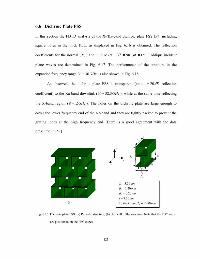
123
6.6 Dichroic Plate FSS
In this section the FDTD analysis of the X-/Ka-band dichroic plate FSS [57] including
square holes in the thick PEC, as displayed in Fig. 6.16 is obtained. The reflection
coefficients for the normal ( zE ) and TE/TM- o30 ( oo 150,90 == ii φθ ) oblique incident
plane waves are determined in Fig. 6.17. The performance of the structure in the
expanded frequency range GHz3631− is also shown in Fig. 6.18.
As observed, the dichroic plate FSS is transparent (about dB20− reflection
coefficient) to the Ka-band downlink ( GHz3.3231− ), while at the same time reflecting
the X-band region ( GHz128 − ). The holes on the dichroic plate are large enough to
cover the lower frequency end of the Ka-band and they are tightly packed to prevent the
grating lobes at the high frequency end. There is a good agreement with the data
presented in [57].
Fig. 6.16: Dichroic plate FSS: (a) Periodic structure, (b) Unit cell of the structure. Note that the PBC walls
are positioned on the PEC edges.
y
z
x
mmTmmTmmt
mmdmmdmmL
zy 80.10,40.620.9
20.020.120.5
2
1
===
===
Ty
L
d2
d1
Tz
t (b) (a)

124
Fig. 6.17: Normal and o30 oblique (TE/TM) incidence reflection coefficient of the dichroic plate FSS.
Fig. 6.18: Performance of the dichroic plate FSS in the expanded frequency range GHz3631− for
the normal and o30 oblique (TE/TM) incidence plane waves.
0.0 5.0 10.0 15.0 20.0 25.0 30.0 35.0 40.0 45.0frequency (GHz)
−50.0
−40.0
−30.0
−20.0
−10.0
0.0
10.0
Refle
ction
Coe
fficien
t (dB)
normal incidenceTE at 30
o
TM at 30o
31.0 32.0 33.0 34.0 35.0 36.0frequency (GHz)
−50.0
−40.0
−30.0
−20.0
−10.0
0.0
10.0
Refle
ction
Coe
fficien
t (dB)
normal incidenceTE at 30
o
TM at 30o

125
6.7 Inset Self-Similar Aperture FSS
The focus of this section is to characterize a dual-band inset self-similar aperture FSS
printed on the dielectric substrate, as shown in Fig. 6.19, utilizing the FDTD/Prony
method. The FSS is constructed from two periodic structures namely, small square
patches and large size square apertures. The characteristics of the small patches (structure
in Fig. 6.19 without metallic strips), large apertures (structure in Fig. 6.19 without
patches), and the composite square patch/square aperture are demonstrated in Fig. 6.20.
As observed, the periodic patches resonant at the high frequencies (stop-band)
while the periodic apertures are able to reject the d.c. frequencies. The composition of
theses two periodic elements produces a dual-band FSS, illustrated in Fig. 6.20. The
FDTD results are compared very well with the measurement data determined in the
UCLA antenna Lab. There is about GHz60 frequency isolation between the stop-bands
of the designed FSS.
The behavior of the structure for the o30 ( oo 150,90 == ii φθ ) TE/TM oblique
incidence plane waves is also explored in Fig. 6.21. As obtained, the performance of the
FSS is sensitive to the polarization and angle of incidence. The TE and TM waves have
different resonance frequencies.

126
Fig. 6.19: Inset self-similar aperture FSS: (a) Periodic structure, (b) Unit cell of the structure. Note that the
PBC walls are positioned on the PEC/dielectric sides.
Fig. 6.20: Normal incidence transmission coefficient of the square patch, square aperture, and inset self-
similar aperture based on the FDTD compared to the measurement data.
0.0 10.0 20.0 30.0 40.0 50.0 60.0 70.0 80.0frequency (GHz)
−30.0
−25.0
−20.0
−15.0
−10.0
−5.0
0.0
5.0
Tran
smiss
ion C
oeffic
ient (d
B)
square patchsquare apertureinset self−similar aperturemeasurements
(b) (a)
mmTmmt
mmdmmd
mmWW
r
1583.0
20.250.1
12
2
1
21
=====
==
ε
y
z
x
T
W1
rε
W2
d1
T
t
d2

127
Fig. 6.21: TE/TM o30 oblique incidence transmission coefficient of the inset self-similar aperture FSS.
6.8 Fractal FSS
Fractal shaped antennas are a new class of self-similar structures with unique
characteristics that are applied into some novel applications. Self-similarity of the fractals
can be described as the replication of the geometry of the structure in different scales
within the same structure. This has a potential advantage in the design of multi-band
frequency selective surfaces [53]. Additionally, the unique shape of the fractal antenna
allows one to confine an arbitrary long curve antenna in a given small area. This property
is very useful in reducing the spacing between the resonance elements in an FSS, and in
reducing the area occupied by the small antennas [58], [59]. This may have the potential
applications in the design of miniaturized antennas.
0.0 10.0 20.0 30.0 40.0 50.0 60.0 70.0 80.0frequency (GHz)
−30.0
−25.0
−20.0
−15.0
−10.0
−5.0
0.0
5.0
Tran
smiss
ion C
oeffic
ient (d
B)
TE caseTM case

128
This section focuses on the characterization of a two-iteration Sierpinski dipole
FSS utilizing the powerful FDTD/Prony engine. The structure is presented in Fig. 6.22.
The transmission coefficient of the free standing fractal FSS for the normal incidence
plane wave ( zE ) is displayed in Fig. 6.23. As obtained, the structure has two resonance
frequencies with the total reflection at 68.5 and GHz39.21 .
The dielectric backed fractal FSS is also analyzed in this section and the results
for both normal and o30 ( oo 150,90 == ii φθ ) oblique incidence (TE case) are
determined in Fig. 6.24. The resonance frequencies for the normal case are located
around 89.3 and GHz15 which are within a 5% error compared to the measurement data
[53]. As observed, the resonance frequencies of the dielectric backed fractal FSS are
shifted down compared to the free standing fractal. The resonance frequencies of the FSS
on the dielectric material can be simply estimated using the following equation
2
1,0+
== raveaved ff εεε (6.1)
where 0f and df are the resonance frequencies of the free standing and dielectric backed
FSS, respectively. The estimated values are around 23.4 and GHz94.15 , which are close
to the computed results.
Although, the FDTD with the rectangular grids are applied to approximate the
triangular edges of the Sierpinski fractal, but still the good agreements with the presented
date in [53] are obtained. Notice that the staircasing with cell size λ01.0 ( λ is the center
frequency) is used to approximate the triangular boundaries.

129
Fig. 6.22: Sierpinski fractal FSS: (a) Free standing fractal, (b) Dielectric backed fractal, (c), (d) Unit cells
of the structures. Note that the PBC walls are positioned on the sides of the structures.
Fig. 6.23: Normal incidence transmission coefficient of the free standing Sierpinski fractal FSS.
2
11.060
21 TddhLTcmh
angleflare
==+=
=
o
y
z
x T
T
t
rεh
d2
d1
L
d1
T
T h
d2
L
cmt
cmL
r
17.060.2
95.1
==
=εcmL 73.1=
(a) (b) (c) (d)
0.0 0.2 0.4 0.6 0.8 1.0 1.2 1.4 1.6 1.8 2.02*L/λ
−30.0
−25.0
−20.0
−15.0
−10.0
−5.0
0.0
5.0
Tran
smiss
ion C
oeffic
ient (d
B)

130
Fig. 6.24: Normal and o30 oblique incidence transmission coefficient of the dielectric backed
Sierpinski fractal FSS.
6.9 Multi-Layered Tripod FSS
In this section, the performance of a multi-layered tripod FSS band-gap structure is
studied. The geometry of a single layer tripod structure is shown in Fig. 6.25. The
FDTD/Prony technique is applied to compute the normal ( zE ) and o30 TE/TM oblique
incidence ( oo 150,90 == ii φθ ) reflected power, as presented in Fig. 6.26. The results are
similar with the data obtained in [54] utilizing MoM. To compare the results with the
measurement data [55], the transmission coefficient at the normal incidence for the tripod
structure printed on the dielectric substrate is determined in Fig. 6.27. There is an
excellent agreement with the measurement data validating the accuracy and capability of
the developed technique.
0.0 5.0 10.0 15.0 20.0 25.0 30.0frequency (GHz)
−30.0
−25.0
−20.0
−15.0
−10.0
−5.0
0.0
5.0
Tran
smiss
ion C
oeffic
ient (d
B)
normal incidence30
o oblique incidence

131
The location of the resonance frequency of the tripod structure can be controlled
using a 2-layer tripod, as presented in Fig. 6.28. The second layer is rotated o180 with
respect to the first layer, and is shifted along the z-axis in such a way that all three legs of
each tripod overlap a leg of a tripod in the first layer. The overlap region forms a
capacitor, which is used to tune the frequency for %100 reflection. The reflected power
of the 2-layer tripod is determined in Fig. 6.29. As observed, compared to the 1-layer
tripod the resonance frequency is shifted down.
To broaden the %100 reflection bandwidth of the tripod structure, a 4-layer
tripod as depicted in Fig. 6.30 (composition of two sets of the structure shown in Fig.
6.28) is introduced. The geometry has two degrees of freedom, d and D . The
capacitance governed by the small distance d controls the lower edge of the rejection
band, where the large inter-capacitor spacing D controls the upper edge of the band. The
reflected power is presented in Fig. 6.31. As observed, by increasing the bandwidth of the
%100 reflection, a band-gap structure utilizing the multiple coupled tripod arrays is
designed. The results agree well with the data presented in [54].
Notice that for the angles near to the grazing, the TM waves are almost normal to
the surface of tripods and the FSS cannot reject them. Utilizing the interconnecting vias
between tripods may help to reject the normal components and design a complete band-
gap structure as achieved in [54].
In this example, the inter-spacing D is much greater than the distance d between
the tripods in each set, and one needs a powerful engine to analyze the structure. The
accurate and efficient results presented in this section, based on the FDTD/Prony method,

132
show the capability of the developed technique in the characterization of complex
structures.
Fig. 6.25: 1-Layer tripod structure: (a) Free standing tripod, (b) Dielectric backed tripod, (c), (d) Unit cells
of the structures. Note that the PBC walls are positioned on the sides of the structures.
(a) (b) (c) (d)
mmTmmTmmLmmLangleflare
z
y
44.240.148.040.0
240
2
1
=
===
o
Ty
L1
L2
Tz
L1
L2
Ty
Tz
t
rε
y
z
x
mmtr
54.020.2
==ε

133
Fig. 6.26: Normal and o30 oblique (TE/TM) incidence reflected power of the 1-layer tripod FSS.
Fig. 6.27: Normal incidence transmission coefficient of the 1-layer tripod FSS printed on the
dielectric substrate.
0.0 20.0 40.0 60.0 80.0 100.0 120.0 140.0 160.0 180.0 200.0frequency (GHz)
−40.0
−35.0
−30.0
−25.0
−20.0
−15.0
−10.0
−5.0
0.0
5.0
Tran
smiss
ion C
oeffic
ient (d
B)
0.0 20.0 40.0 60.0 80.0 100.0 120.0 140.0 160.0 180.0 200.0frequency (GHz)
0.0
10.0
20.0
30.0
40.0
50.0
60.0
70.0
80.0
90.0
100.0
110.0
% of
Powe
r Refl
ected
normal incidenceTE at 30
o
TM at 30o

134
Fig. 6.28: 2-Layer tripod structure: (a) Periodic structure, (b) Unit cell of the structure. Note that the PBC
walls are positioned on the PEC edges.
Fig. 6.29: Normal and o30 oblique (TE/TM) incidence reflected power of the 2-layer tripod FSS.
(b) (a)
mmTmmTmdmmW
zy 44.2,40.120
40.0
====
µ
y
z
x
W
d
Tz
Ty
0.0 20.0 40.0 60.0 80.0 100.0 120.0 140.0 160.0 180.0 200.0frequency (GHz)
0.0
10.0
20.0
30.0
40.0
50.0
60.0
70.0
80.0
90.0
100.0
110.0
% of
Powe
r Refl
ected
normal incidenceTE at 30
o
TM at 30o

135
Fig. 6.30: 4-Layer tripod structure (composition of two sets of the structure shown in Fig. 6.28): (a)
Periodic structure, (b) Unit cell of the structure. Note that the PBC walls are positioned on the
PEC edges.
Fig. 6.31: Normal and o30 oblique (TE/TM) incidence reflected power of the 4-layer tripod EBG structure.
(b) (a)
mmTmmTmmD
mdmmW
zy 44.2,40.1120
40.0
=====
µ
W
D
d
Tz
Ty
y
z
x
0.0 20.0 40.0 60.0 80.0 100.0 120.0 140.0 160.0 180.0 200.0frequency (GHz)
0.0
10.0
20.0
30.0
40.0
50.0
60.0
70.0
80.0
90.0
100.0
110.0
% of
Powe
r Refl
ected
normal incidenceTE at 30
o
TM at 30o

136
6.10 9-Layer Dielectric/Inductive Square Loop FSS
A 9-layer dielectric/inductive square loop pass-band FSS, designed by Munk [11], is
characterized in this section. The structure is the composition of 2-layer cascaded
inductive square loop FSS sandwiched between the 7 layer dielectric materials, as
depicted in Fig. 6.32. The broadband analysis of the complex structure is obtained using
the FDTD/Prony technique.
The transmission coefficients of the 2-layer square loop, 7-layer dielectric
material, and the composite square loop/dielectric material for the normal and o30
TE/TM oblique incidence ( oo 150,90 == ii φθ ) plane waves are presented in Figs. 6.33,
6.34, and 6.35, respectively.
The inductive square loop FSS has the property to pass the EM waves at the
resonance frequency. To generate a frequency response with an almost flat-top or gap
region, 2 layers of the FSS are cascaded, as obtained in Fig. 6.32a with the transmission
coefficient in Fig. 6.33. Additionally as observed in Fig. 6.34, the properly layered
dielectric materials have the potential to effectively produce the pass/stop band regions
for the EM waves. Sandwiching the cascaded FSS layers between the dielectric slabs
(Fig. 6.32c) presents a novel metallo-dielectric periodic structure with the improved
electromagnetic gap region, as demonstrated in Fig. 6.35. The composite structure
provides a frequency performance with an almost constant bandwidth and flat gap region
for the plane waves incident on the structure. Increasing the number of FSS layers and
using more suitable layered dielectric materials may improve the band-gap characteristics
of the structure.

137
Fig. 6.32: 9-Layer dielectric/inductive square loop FSS: (a) 2-Layer inductive square loop, (b) 7-Layer
dielectric material, (c) Composite square loop/dielectric material (9 layers), (d) Cross section
of the layered structure, (e) Unit cell of the square loop FSS.
(a) (b) (c) (d)
(e)
xy
z
mmtmmt
LoopSquareInductivemmtmmt
mmtLoopSquareInductive
mmtmmt
92.7,50.4:9#99.0,2:8#
:7#49.1,2:6#96.3,14:5#
49.1,2:4#:3#
99.0,2:2#92.7,50.4:1#
99
88
66
55
44
22
11
====
====
==
====
εε
εεε
εε
T
W
d1
d2
T
#1#2
.
.
.
#9x
z
y
z
mmTmmdmmdmmW
86.1449.099.087.13
2
1
====

138
Fig. 6.33: Normal and o30 oblique (TE/TM) incidence transmission coefficient of the 2-layer inductive
square loop FSS.
Fig. 6.34: Normal and o30 oblique (TE/TM) incidence transmission coefficient of the 7-layer
dielectric material.
0.0 2.0 4.0 6.0 8.0 10.0 12.0 14.0 16.0 18.0frequency (GHz)
−30.0
−25.0
−20.0
−15.0
−10.0
−5.0
0.0
5.0
Tran
smiss
ion C
oeffic
ient (d
B)
normal incidenceTE at 30
o
TM at 30o
0.0 2.0 4.0 6.0 8.0 10.0 12.0 14.0 16.0 18.0frequency (GHz)
−30.0
−25.0
−20.0
−15.0
−10.0
−5.0
0.0
5.0
Tran
smiss
ion C
oeffic
ient (d
B)
normal incidenceTE at 30
o
TM at 30o

139
Fig. 6.35: Normal and o30 oblique (TE/TM) incidence transmission coefficient of the 9-layer
dielectric/inductive square loop FSS.
6.11 Smart Surface Mushroom FSS
The mushroom band-gap structure proposed by Yablonovitch [60] is another novel
design of the periodic structures. This structure has the potential to present an effective
smart surface with the frequency variable reflection phase; and additionally it is able to
suppress the surface waves successfully. The geometry of the structure, as depicted in
Fig. 6.36, consists of a lattice of metallic patches connected to a metallic sheet by the
vertical conducting vias. There is a dielectric material between the metallic plates.
The FDTD/Prony technique is applied to characterize the structure for the normal
and oblique incidence TE waves. The reflection coefficient is equal to one similar to the
0.0 2.0 4.0 6.0 8.0 10.0 12.0 14.0 16.0 18.0frequency (GHz)
−30.0
−25.0
−20.0
−15.0
−10.0
−5.0
0.0
5.0
Tran
smiss
ion C
oeffic
ient (d
B)
normal incidenceTE at 30
o
TM at 30o

140
PEC ground plane. However, the reflection phase on the surface of the mushrooms, as
observed in Fig. 6.37, has a frequency variation defining an effective surface with the
smart property from PEC to PMC. This has the potential application for the low profile
antenna designs, where the antenna can be brought very close to the %100 reflecting
surface and still match the antenna and obtain a very good radiation characteristic.
The possibility of suppressing the surface waves utilizing the mushroom FSS
structure is also explored in this work. In this manner, the performance of the 2 layers
patch/via metallic elements shown in Fig. 6.38(a), for the normal and oblique incident TE
waves propagating in the transverse plane ( 0=izk ) is investigated. Notice that, in order
to characterize the structure based on the developed FDTD technique, the geometry is
assumed to be periodic in the z-direction. The grating PEC layers without the patches and
vias (Fig. 6.38(b)) totally transmit the z-polarized incident waves, and no reflection
occurs on the surface of the layered PEC. However, by adding the mushroom structure
(Fig. 6.38(a)) an electromagnetic band-gap region for the surface waves is opened up
which forbids the propagation of the EM waves in all directions in the transverse plane,
as illustrated in Fig. 6.39.
Thus, the mushroom EBG, a metallo-dielectric band-gap structure, has the
potential to generate a smart surface with the novel reflection phase properties from PEC
to PMC. In addition, it can provide a complete surface wave band-gap region to
effectively prevent the propagation of the EM waves in the transverse plane. These can
be properly incorporated into the design of low profile antennas with the strongly reduced
edge diffraction effects [60], [61].

141
Fig. 6.36: Mushroom EBG: (a) Periodic structure, (b) Unit cell of the structure. Note that the PBC
walls are positioned on the PEC edges.
Fig. 6.37: Normal and oblique incidence reflection phase of the mushroom EBG structure. Note the phase
variation from PEC to PMC. Reflection phase is computed on the surface of mushrooms.
0.0 5.0 10.0 15.0 20.0 25.0 30.0 35.0 40.0 45.0 50.0frequency (GHz)
−200.0
−150.0
−100.0
−50.0
0.0
50.0
100.0
150.0
200.0
Refle
ction
Pha
se (d
eg.)
normal incidence30
o oblique incidence
60o oblique incidence
|ϕϕϕϕ| < 90o
|ϕϕϕϕ| > 90o
|ϕϕϕϕ| > 90o
(b) (a)
y
z
x
mmT
mmwmmDmmWmmW
r
40.220.230.058.125.240.2
2
1
======
ε
T
T
W1
rε
D
w
W2
dielectric

142
Fig. 6.38: Suppression of the surface waves: (a) 2-Layer mushroom EBG, (b) PEC grating layers.
Note that the structures are periodic in the y-z directions.
Fig. 6.39: Normal and oblique incidence reflection coefficient of the 2-layer mushroom EBG structure.
Notice that the mushroom EBG opens up a complete surface waves band-gap region.
0.0 5.0 10.0 15.0 20.0 25.0 30.0 35.0 40.0 45.0 50.0frequency (GHz)
−50.0
−40.0
−30.0
−20.0
−10.0
0.0
10.0
Refle
ction
Coe
fficien
t (dB)
normal incidence30
o oblique incidence
60o oblique incidence
(a) (b)
y
z
x
. . . . . .
. . . . . .

143
6.12 Summary
In this chapter, the FDTD/Prony technique is applied to characterize and obtain the
propagation performance of some of the challenging and applicable frequency selective
surfaces composed of arbitrary dielectric/metallic structures.
The broadband analysis of the periodic structures namely, layered dielectric
materials, double concentric square loop FSS, dipole FSS manifesting high Q resonance,
square patch FSS manifesting high Q resonance, crossed dipole FSS, dichroic plate FSS,
inset self-similar aperture FSS, Sierpinski fractal FSS, layered tripod FSS, 9-layer
dielectric/inductive square loop FSS, and smart surface mushroom FSS is successfully
presented. The results are extremely satisfactory demonstrating the capability of the
developed method in the broadband analysis of complex structures. Notice that the
Pronys scheme has been also applied to obtain the frequency response of the structures
with much more accuracy and efficiency.
Also, in this work, the creation of the band-gap structures utilizing the cascaded
FSS layers sandwiched between the dielectric slabs is investigated. Furthermore, the
novel performance of the smart surface mushroom EBG, which has the potential
applications in the communication antenna systems, is highlighted.

144
Chapter 7
Photonic Band-Gap Structures
Photonic band-gap structures are typically a class of periodic dielectric materials, which
by generating an electromagnetic band-gap forbid the propagation of EM waves. The
discovery of photonic band-gap materials has created unique opportunities for controlling
the propagation of EM waves, leading to numerous novel applications in the optical and
microwave technologies [62]-[68].
In this chapter, a comprehensive treatment of these potentially useful band-gap
structures is provided. The objective is to characterize their interaction with the
electromagnetic waves, identify their innovative propagation performances, incorporate
the results into potential applications, and explore the possibility of modeling their
characteristics using effective dielectric materials.
To accomplish this, the FDTD/Prony technique is applied to obtain and
understand the band-gap behaviors of the triangular, rectangular, and woodpile PBG
structures. The results are incorporated into three potential applications, namely, design
of high Q nanocavity lasers, guiding the EM waves in sharp bends, and miniaturized
microstrip patch antennas. The effective dielectric material concept is also applied to
investigate the possibility of modeling the performance of PBG using effective dielectric.

145
7.1 Band-Gap Characterization of PBG
The focus of this section is to present and study the band-gap characteristics of the PBG
structures utilizing the FDTD/Prony technique. In this work, to obtain the performance of
the PBG, the reflection coefficient of the plane wave incident on the band-gap structure is
determined. Compared to the dispersion diagram method, which is usually applied to
analyze these structures, the present technique appears to have two potential advantages:
• Obtaining reflection and/or transmission coefficients outside the band-gap regime,
• Presenting phase and polarization information of the scattered fields.
Obviously, using dispersion diagrams, it is not possible to obtain the reflection
and transmission coefficients for the frequencies outside the band-gap. Additionally,
phase and polarization of the reflected field cannot be deduced from a dispersion
diagram. However, using the dispersion diagram one can effectively study the modal
properties of the EM waves.
Notice that in the characterization of the periodic dielectric PBG structures, in
order to keep the consistency with other chapters of this dissertation, the TE modes are
defined as the waves where the electric field does not have any component in the
direction normal to the surface of the periodic structure (x-direction); while the TM
modes are the waves where the magnetic field does not have any component in the
direction normal to the surface of the structure. These definitions are pictorially
illustrated in Fig. 7.1 for a 2-D periodic triangular PBG structure of 5-layer infinite
dielectric columns.
146
7.1.1 Triangular PBG
A 2-D periodic triangular PBG structure of 5-layer infinite dielectric columns inside the air
region is depicted in Fig. 7.2. The structure is accurately analyzed using the FDTD
technique, and the results for the normal and oblique incidence (in-plane angle) reflection
coefficient are obtained in Fig. 7.3. As illustrated, there is a band-gap region for the waves
polarized along the axis of the columns (TE band-gap) for the normalized frequencies
30.023.0 0 ≤≤ λa . The location of the band-gap region has an excellent agreement with
the data presented in [12] based on the dispersion diagram.
The complementary geometry of Fig. 7.2 is presented in Fig. 7.4. The structure is a
5-layer PBG structure of air holes drilled in the dielectric material. The plane wave
reflection coefficient is determined in Fig. 7.5. As shown, compared to the previous
structure the connectivity in the high dielectric material is able to generate the TM band-
gap (gap for the waves polarized in the transverse plane) in the normalized frequency range
26.020.0 0 ≤≤ λa .
The periodic contrast between the dielectric-air regions is the key for generating the
band-gap. This contrast in the isolated (Fig. 7.2) or connected (Fig. 7.4) dielectric PBG
results in the contrast of the energy confinement between the lower and upper band-gap
edges for the TE or TM modes, respectively.
7.1.2 Rectangular PBG
The performance of a 2-D periodic rectangular PBG structure of 5-layer infinite dielectric
columns inside the air region, as shown in Fig. 7.6, for the normal and oblique incidence
147
plane waves is determined in Fig. 7.7. As expected, a TE band-gap region for the
normalized frequencies 32.022.0 0 ≤≤ λa is achieved.
To obtain the TM band-gap region, a rectangular lattice of air holes drilled in the
dielectric medium is presented in Fig. 7.8. The connectivity of the dielectric material
opens up the gap regions for the TM waves determined in Fig. 7.9. It is demonstrated in
Fig. 7.10 that by increasing the size of the holes the dielectric filling ratio of the PBG is
reduced and the structure can be considered as the dielectric spots surrounded by the air
holes. In this case, the near isolation of the dielectric columns is crucial to the production
of gap region for the TE waves. The TE band-gap behavior of the structure for the
frequency range 26.020.0 0 ≤≤ λa is displayed in Fig. 7.11.
A rule of thumb may be developed that, the TE band-gaps are favored in a lattice
of isolated high dielectric regions while the TM band-gaps are favored in a connected
lattice. Arranging the PBG structure with both isolated spots and connected regions of
dielectric material may results in the novel designs with complete band-gap regions [12].
7.1.3 Woodpile PBG
The woodpile PBG structure proposed by Ho et al. [69], is a novel design of the 3-D
periodic dielectric materials with the complete band-gap region. The geometry of a 2-layer
infinite square dielectric rods woodpile PBG is shown in Fig. 7.12. The structure is a
composition of both separated and connected high dielectric regions in the three directions,
which has the potential to generate a complete band-gap region and forbid the
electromagnetic wave propagation in almost all directions.

148
The reflection coefficient for the normal, o30 oblique/TE, and arbitrary incident
plane wave oo 150,40 == ii φθ with polarization angle o45=iψ is presented in Fig.
7.13. As demonstrated, the structure is able to generate an almost complete band-gap
region independent of the angle and polarization of the incident wave. By increasing the
number of the periodic layers one can design a structure with the better band-gap
performance.
The phase behavior of the reflected field on the surface of the woodpile for the
o30 oblique wave is investigated in Fig. 7.14. It is observed that, within the gap region the
phase has an almost linear frequency variation. Thus, inside the band-gap, the woodpile
structure may be modeled using an effective PEC plane where its location is variable
(depend on the incident angle) instead to be fixed at the front surface of PBG. In some
situations, the effective reflection plane concept is a valuable tool to approximate the
performance of the PBG using the effective PEC plane [70].
7.1.4 Effective Dielectric Material
The objective in this section is to explore the possibility of modeling the behavior of the
periodic dielectric PBG structure using the effective dielectric material. Based on the
effective medium concept, the effective dielectric effε of the periodic composite structure
of air/dielectric regions at long wavelengths can be approximated using the equation [71],
[72]
ardreff ff εεε ⋅−+⋅= )1( (7.1)

149
where rf is the dielectric filling ratio, and dε and aε are the dielectric constants of the
material and air ( 1=aε ) regions, respectively (Fig. 7.15).
The rectangular PBG structure of the isolated dielectric columns (Fig. 7.6, TE band-
gap) is modeled using the one-dimensional periodic air/dielectric multi-layered structure in
Fig. 7.16. The layered planar structure is analyzed based on the vector wave solution of
Maxwells equations (Chapter 2). The band-gap characteristics of the triangular and
rectangular PBG are compared with the effective dielectric model in Fig. 7.17, for the o60
oblique incidence wave. The periodic isolated dielectric layers of the effective model
create a TE band-gap region illustrated in Fig. 7.17. For the small values of the lattice
constant a the PBG and effective dielectric has almost the similar performance.
However, by increasing the lattice constant and especially inside the gap region, the
effective dielectric cannot model the PBG structure.
The behaviors of the triangular and rectangular PBG of the connected lattice are
compared with the effective dielectric model (Fig. 7.18) in Fig. 7.19. In this case, the TM
band-gap performance of the PBG is based on the connectivity in the high dielectric
material; while the effective medium is a composition of the isolated dielectric layers and
obviously it cannot model the characteristics of the PBG as illustrated in Fig. 7.19.

150
(a) TE Mode
(b) TM Mode
Fig. 7.1: Pictorially illustration of the (a) TE ( zE ), and (b) TM ( zH ) waves definitions for a
2-D triangular PBG structure including of 5-layer dielectric columns.
y
z
x
Ei
Hi
#1
#5
#3 #4
#2
. . . . . . . . .
. . .
y
z
x
Hi
Ei
#1
#5
#3 #4
#2
. . . . . .
. . . . . .

151
Fig. 7.2: 2-D triangular PBG structure including of 5-layer dielectric columns (finite in x direction, infinite
in y-z directions): (a) Periodic structure, (b) Unit cell of the structure. Note that the PBC walls are
positioned on the dielectric sides.
Fig. 7.3: Normal and oblique incidence reflection coefficient of the triangular PBG of dielectric columns.
The isolated dielectric regions open up the TE ( zE ) band-gap.
0.00 0.05 0.10 0.15 0.20 0.25 0.30 0.35 0.40a/λ0
−50.0
−40.0
−30.0
−20.0
−10.0
0.0
10.0
Refle
ction
Coe
fficien
t (dB)
normal incidence30
o oblique incidence
60o oblique incidence
. . .
y
z
x
aTaT
ar
zy
r
20.0,3
28.040.11
==
==ε
Tz
Ty
a r
(b) (a)
#1
#5
#3 #4
#2
. . .
. . . . . .
εr

152
Fig. 7.4: 2-D triangular PBG structure including of 5-layer air holes (finite in x direction, infinite in y-z
directions): (a) Periodic structure, (b) Unit cell of the structure. Note that the PBC walls are
positioned on the dielectric sides.
Fig. 7.5: Normal and oblique incidence reflection coefficient of the triangular PBG of air holes. The
connected dielectric regions open up the TM ( zH ) band-gap.
0.00 0.05 0.10 0.15 0.20 0.25 0.30 0.35 0.40a/λ0
−50.0
−40.0
−30.0
−20.0
−10.0
0.0
10.0
Refle
ction
Coe
fficien
t (dB)
normal incidence30
o oblique incidence
60o oblique incidence
(b) (a)
y
z
x
aTaT
ar
zy
r
20.0,3
28.040.11
==
==ε
r a
Tz
Ty
#1
#5
#3 #4
#2
. . . . . .
. . . . . .
εr

153
Fig. 7.6: 2-D rectangular PBG structure including of 5-layer dielectric columns (finite in x direction,
infinite in y-z directions): (a) Periodic structure, (b) Unit cell of the structure. Note that
the PBC walls are positioned on the dielectric sides.
Fig. 7.7: Normal and oblique incidence reflection coefficient of the rectangular PBG of dielectric columns.
The isolated dielectric regions open up the TE ( zE ) band-gap.
0.00 0.05 0.10 0.15 0.20 0.25 0.30 0.35 0.40a/λ0
−50.0
−40.0
−30.0
−20.0
−10.0
0.0
10.0
Refle
ction
Coe
fficien
t (dB)
normal incidence30
o oblique incidence
60o oblique incidence
y
z
x
aTaTar
zy
r
20.0,28.0
40.11
====ε
(b) (a)
Tz
Ty
ar
#1
#5
#3 #4
#2
. . . . . .
. . . . . .
εr

154
Fig. 7.8: 2-D rectangular PBG structure including of 5-layer air holes (finite in x direction, infinite in y-z
directions): (a) Periodic structure, (b) Unit cell of the structure. Note that the PBC walls are
positioned on the dielectric sides.
Fig. 7.9: Normal and oblique incidence reflection coefficient of the rectangular PBG of air holes. The
connected dielectric regions open up the TM ( zH ) band-gap.
0.00 0.05 0.10 0.15 0.20 0.25 0.30 0.35 0.40a/λ0
−50.0
−40.0
−30.0
−20.0
−10.0
0.0
10.0
Refle
ction
Coe
fficien
t (dB)
normal incidence30
o oblique incidence
60o oblique incidence
(b) (a)
y
z
x
aTaTar
zy
r
20.0,39.0
40.11
====ε
Ty
Tz
r a
#1
#5
#3 #4
#2
. . . . . .
. . . . . .
εr

155
Fig. 7.10: 2-D rectangular PBG structure including of 5-layer large size air holes (finite in x direction,
infinite in y-z directions): (a) Periodic structure, (b) Transverse plane representing the
dielectric spots surrounded by the air holes, (c) Unit cell of the structure. Note that the PBC
walls are positioned on the dielectric sides.
Fig. 7.11: Normal and oblique incidence reflection coefficient of the rectangular PBG of air holes. The
large size of the air holes generates the isolated dielectric columns opening up the TE ( zE )
band-gap.
0.00 0.05 0.10 0.15 0.20 0.25 0.30 0.35 0.40a/λ0
−50.0
−40.0
−30.0
−20.0
−10.0
0.0
10.0
Refle
ction
Coe
fficien
t (dB)
normal incidence30
o oblique incidence
60o oblique incidence
(a) (c) (b)
Ty
Tz
ar
y
z
x
aTaTar
zy
r
20.0,45.0
40.11
====ε
dielectric spot
#1
#5
#3 #4
#2
. . . . . .
. . . . . .
εr

156
Fig. 7.12: 2-Layer square dielectric rods woodpile PBG structure (finite in x direction, infinite in y-z
directions): (a) Periodic structure, (b) Unit cell of the structure. Note that the PBC walls are
positioned on the dielectric sides.
Fig. 7.13: Normal and oblique incidence reflection coefficient of the square dielectric rods woodpile PBG.
Proper arrangements of the isolated and connected dielectric regions open up an almost
complete band-gap.
0.0 0.1 0.2 0.3 0.4 0.5 0.6 0.7a/λ0
−50.0
−40.0
−30.0
−20.0
−10.0
0.0
10.0
Refle
ction
Coe
fficien
t (dB)
normal incidenceθi
=90o, φi
=150o, ψi
=90o
θi=40
o, φi
=150o, ψi
=45o
(b) (a)
aTaw
r
===
29.000.8ε
T
T
w
T/2
T/2
y
z
x
#1 #2
. . . . . .
. . . . . .
εr

157
Fig. 7.14: o30 incidence reflection phase of the square dielectric rods woodpile PBG. Reflection phase is
computed on the surface of structure. Notice that the phase has an almost linear frequency
variation within the band-gap.
(a) (b)
Fig. 7.15: Effective dielectric model for composite periodic structure of air/dielectric regions: (a) Periodic
structure, (b) Effective dielectric material.
0.0 0.1 0.2 0.3 0.4 0.5 0.6 0.7a/λ0
−200.0
−150.0
−100.0
−50.0
0.0
50.0
100.0
150.0
200.0
Refle
ction
Pha
se (d
eg.)
Linear
effεdε
triangleofareatriangletheinsideregiondielectricofarea
f r =

158
Fig. 7.16: Multi-layered one-dimensional periodic dielectric structure (finite in x direction, infinite in y-z
directions). Effective dielectric model for the isolated columns rectangular PBG in Fig. 7.6.
Fig. 7.17: Comparative study between the performance of triangular and rectangular isolated columns PBG
with the effective dielectric model for the o60 oblique incidence TE wave ( zE ).
0.00 0.05 0.10 0.15 0.20 0.25 0.30 0.35 0.40a/λ0
−50.0
−40.0
−30.0
−20.0
−10.0
0.0
10.0
Refle
ction
Coe
fficien
t (dB)
triangular PBGrectangular PBGEFFD
y
z
x
atat
45.0,00.155.0,40.5
22
11
====
εε
11 , tε
22 , tε
a
. . . . . .
. . . . . .

159
Fig. 7.18: Multi-layered one-dimensional periodic dielectric structure (finite in x direction, infinite in y-z
directions). Effective dielectric model for the connected lattice rectangular PBG in Fig. 7.8.
Fig. 7.19: Comparative study between the performance of triangular and rectangular connected lattice PBG
with the effective dielectric model for the o60 oblique incidence TM wave ( zH ).
0.00 0.05 0.10 0.15 0.20 0.25 0.30 0.35 0.40a/λ0
−50.0
−40.0
−30.0
−20.0
−10.0
0.0
10.0
Refle
ction
Coe
fficien
t (dB)
triangular PBGrectangular PBGEFFD
y
z
x
atat
22.0,40.1178.0,06.5
22
11
====
εε
a
11 , tε
22 , tε . . . . . .
. . . . . .

160
7.2 Representative Applications of PBG
In this section, the novel characteristics of the PBG structure are integrated into the three
representative applications, namely, high Q nanocavity lasers, guiding the EM waves in
sharp bends, and miniaturized microstrip patch antennas. A comparative study between
the PBG and effective dielectric in the design of cavity, waveguide, and patch antenna is
also presented. It is obtained that the performance of the PBG within the band-gap region
cannot be modeled using the effective dielectric materials.
7.2.1 High Q Nanocavity Lasers
Confinement of the electromagnetic waves in a very small volume has important
consequences in the property of the optical emission such as reduction in size and power
requirement of the integrated optical components, controlling spontaneous emission, and
higher modulation speeds [73]-[76]. The goal of this section is to study a high Q
nanocavity laser using the PBG structure and compare its performance with the effective
dielectric model.
A. PBG Cavity
To design a high Q nanocavity laser a finite thickness 2-D PBG structure is used to
localize the electromagnetic waves inside a defect region in three directions, based on the
PBG gap/total internal reflections [75]. The defect-excited mode (inside the gap region)
is localized in the transverse plane utilizing the PBG structure. In the vertical direction,
161
the dielectric contrast between the impurity and outside air region generates the total
internal reflections as it traps the waves in this direction.
Fig. 7.20 shows a 2-D PBG structure including 3-layer photonic cells of the
triangular lattice of air holes drilled in a dielectric host medium with 56.11=hε (which
corresponds to GaAs) and slab thickness ad 57.0= . The air holes have the radius
ar 29.0= . This structure generates a TM band-gap for the electric field polarized in the
plane of periodicity. The center hole of the PBG is removed to generate a defect region
and is excited by a y-directed infinitesimal dipole. The y-dipole mode cannot propagate
through the PBG in the transverse plane and in the vertical direction it is trapped by the
way of total internal reflection at the dielectric-air interfaces. The EM fields are localized
inside the defect and at the resonance frequency generate a high Q dielectric nanocavity
laser.
The characterization of the finite size PBG structure is obtained based on the
FDTD technique. The resonance frequency is determined at THzf 1280 = (infrared),
where 29.00 =λa (notice that the mid-gap frequency for a finite thickness PBG
compared to the infinite one is increased [75]). Figs. 7.21(a) and 7.21(b) show the near
field patterns of the PBG structure in the transverse and vertical planes, respectively. As
observed the EM waves are trapped in the defect region by the periodic PBG /total
internal reflection.

162
B. Effective Dielectric Cavity
To investigate the possibility of modeling the PBG in confining the EM waves using
effective medium concept, the periodic structure is replaced by an effective dielectric
(Eq. (7.1)), as shown in Fig. 7.22. Two different cases are followed to present the
comparative study between the PBG and effective dielectric:
Case I (inside the band-gap): In this case the PBG structure, operating within the gap
region, with %31 air filling ratio is replaced by an effective dielectric 29.8=effε (the
defect dielectric constant is the same as before, 56.11=defε ). The near field patterns of
the effective dielectric in the transverse and vertical planes are plotted in Figs. 7.23(a)
and 7.23(b). As observed, compared to the PBGs patterns (Fig. 7.21), in the transverse
plane the EM waves propagate outside the defect region without any strong reflection on
the boundary of the cavity; however, in the vertical plane the waves are trapped similar to
the PBG. To design a high Q cavity, one needs a strong reflection on the circular wall of
the cavity to localize the EM waves in the transverse plane. Therefore, in this case the
effective dielectric cannot properly model the PBG for localizing the EM waves.
Case II (outside the band-gap): In the second case the performance of the PBG is
compared with the effective dielectric model for the normalized frequencies outside the
band-gap. A PBG structure with ad 66.0= , ar 33.0= , and 012.0 λ=a is designed to
operate at THzf 1240 = outside the gap region. The structure with %40 air filling ratio

163
is modeled using the effective material 34.7=effε . Figs. 7.24(a) and 7.24(b) display the
field patterns in the transverse plane for both PBG and effective dielectric structures. As
observed, since the PBG operates outside the gap region, both structures have almost the
same behaviors and they cannot localize the EM waves.
It is concluded that for the frequencies within the band-gap, where the lattice
constant is in the order of dielectric wavelength, the PBG cannot be modeled using the
effective dielectric; however, outside the band-gap with small lattice constants (compared
to the dielectric wavelength), the PBG and effective dielectric have almost similar
behaviors.
The concept of PBG in localizing the EM waves is based on creation a band-gap
with an almost 100% reflection in all directions, and then the defect excited modes within
the band-gap region in not able to propagate through the PBG. But, the effective
dielectric medium controls the propagation of the EM waves based on total internal
reflection, which it cannot be occurred in all directions on the circular boundary of the
cavity. To increase the trapping of the EM waves using the effective dielectric medium,
one can increase the contrast between the defect and effective material. Fig. 7.25 shows
the field pattern of the effective dielectric 29.8=effε with relatively large defect region
49=defε , and as observed the waves are almost confined inside the cavity.
The electric and magnetic energy densities eW and mW inside the cavity region
can be determined by the following equations
2
2Eε=eW (7.2a)

164
⋅= 2
2Hµ
mW (7.2b)
Using these equations the total stored energy inside the defect region for three different
cases, PBG/inside the band-gap and effective material 29.8=effε with two different
defect dielectrics 56.11=defε and 49=defε is computed in Fig. 7.26. The slope of the
exponential decay of the energy can be used to obtain the quality factor (Q) of the cavity.
Note that, this method is useful where the Q of the system is not very large. It is shown
that the PBG structure generates the highest quality factor with 116=Q .
C. 7-Layer High Q PBG Structure
As mentioned earlier, the Q of the PBG is controlled by the periodic structure in the
transverse direction ( ||Q ) and total internal reflection in the vertical direction ( ⊥Q ). The
total Q is calculated using the following equation:
⋅+=⊥QQQ
111
||
(7.3)
The ||Q is increased by using more number of photonic cells, and the ⊥Q is controlled by
changing the defect dielectric constant as it controls the trapping of the EM waves in the
vertical direction. To design a high Q nanocavity laser both ||Q and ⊥Q should have the
large values.
Fig. 7.27 depicts a 7-layer photonic cells PBG structure with ad 50.0= and
ar 31.0= . Total stored energy inside the defect region is obtained in Fig. 7.28. In the
first case a defect region with the same dielectric constant as the host medium

165
( 56.11== hdef εε ) is used. Since in this design the number of photonic cells is increased
to 7 layers, the quality factor is also increased to about 210=Q at the normalized
frequency 30.00 =λa ( THzf 1250 = ).
By varying the defect dielectric constant, both defect band frequency and total Q
of the structure are changed, as determined in Figs. 7.29 and 7.30. It is obtained that at
the normalized frequency 346.00 =λa ( 0.4=defε ), a relatively high Q structure is
designed and the modes are strongly localized and cannot be leaked to the outside region.
The quality factor for this excited defect band ( 346.00 =λa , THzf 1400 = ) is about
1050=Q .

166
(a) (b)
Fig. 7.20: Cavity design using finite thickness 2-D triangular PBG structure: (a) 3-D geometry, (b) Cross
section of the PBG (x-y plane).
(a) (b)
Fig. 7.21: Near field patterns of the PBG: (a) Transverse plane, (b) Vertical plane.
Fig. 7.22: Effective dielectric model for the PBG periodic structure.
0.0 0.5 1.0 1.5 2.0 2.5 3.0 3.5 4.0 4.50.0
0.5
1.0
1.5
2.0
2.5
3.0
3.5
4.0
x (micrometer)
y (m
icro
met
er)
120.0 140.0 160.0 180.0
E (dB)
160.0
130.0
150.0
0.0 0.5 1.0 1.5 2.0 2.5 3.0 3.5 4.0 4.50.0
0.2
0.4
0.6
0.8
1.0
1.2
1.4
x (micrometer)
z (m
icro
met
er)
120.0 140.0 160.0 180.0
E (dB)
140.0
150.0
160.0
effective dielectric defect region
d
r a
x
y
y
z
x

167
(a) (b)
Fig. 7.23: Near field patterns of the effective dielectric as it models the PBG (inside the band-gap):
(a) Transverse plane, (b) Vertical plane. Note the lack of similarity between the field
patterns of effective dielectric and PBG (Fig. 7.21(a)) in transverse plane.
(a) (b)
Fig. 7.24: Near field patterns of the (a) PBG (outside the band-gap) compared to the (b) effective dielectric.
Note the similarity between the field patterns.
0.0 0.5 1.0 1.5 2.0 2.5 3.0 3.5 4.0 4.50.0
0.5
1.0
1.5
2.0
2.5
3.0
3.5
4.0
x (micrometer)
y (m
icro
met
er)
120.0 140.0 160.0 180.0
E (dB)
140.0
130.0
150.0
0.0 0.5 1.0 1.5 2.0 2.5 3.0 3.5 4.0 4.50.0
0.2
0.4
0.6
0.8
1.0
1.2
1.4
x (micrometer)
z (m
icro
met
er)
120.0 140.0 160.0 180.0
E (dB)
130.0
140.0
150.0
0.0 0.5 1.0 1.5 2.00.0
0.5
1.0
1.5
x (micrometer)
y (m
icro
met
er)
120.0 140.0 160.0 180.0
E (dB)
150.0
140.0
160.0
0.0 0.5 1.0 1.5 2.00.0
0.5
1.0
1.5
x (micrometer)
y (m
icro
met
er)
120.0 140.0 160.0 180.0
E (dB)
140.0
150.0
160.0

168
Fig. 7.25: Near field pattern of the effective dielectric material in the transverse plane with a relatively
high dielectric defect region. The waves are almost confined inside the cavity.
Fig. 7.26: Total stored energy inside the defect region for the PBG compared to the effective dielectric
materials. Note that the PBG has the highest quality factor.
0.0 0.5 1.0 1.5 2.0 2.5 3.0 3.5 4.00.0
0.5
1.0
1.5
2.0
2.5
3.0
3.5
4.0
x (micrometer)
y (m
icro
met
er)
120.0 140.0 160.0 180.0
E (dB)
130.0
140.0
150.0
0.00 0.05 0.10 0.15 0.20Time (ps)
10−2
100
102
104
106
108
1010
Total
Ene
rgy (A
U)
PBGεeff=8.29, εdef=11.56εeff=8.29, εdef=49
Q=6
Q=116
Q=77

169
Fig. 7.27: High Q nanocavity laser utilizing 7-layer PBG structure.
Fig. 7.28: Total stored energy inside the defect region of the 7-layer PBG for the same and
different defect dielectrics (compared to the host medium).
0.0 0.1 0.2 0.3 0.4 0.5Time (ps)
100
102
104
106
108
1010
Total
Energ
y (AU
)
same defect dielectric (εdef=11.56)different defect dielectric (εdef=4.00)
Q=1050
Q=210

170
Fig. 7.29: Defect band frequency of the 7-layer PBG for various defect dielectrics.
Fig. 7.30: Total Q of the 7-layer PBG versus normalized frequency (varying defect dielectric).
Notice that the maximum Q ( 1050=Q ) occurs around the normalized frequency
346.00 =λa ( 0.4=defε ).
1.0 2.0 3.0 4.0 5.0 6.0 7.0 8.0 9.0 10.0 11.0 12.0Defect Dielectric Constant (εdef)
0.300
0.310
0.320
0.330
0.340
0.350
0.360
0.370
Norm
alize
d Freq
uenc
y (a/λ
0)
0.300 0.310 0.320 0.330 0.340 0.350 0.360 0.370Normalized Frequency (a/λ0)
200
400
600
800
1000
1200
Total
Q

171
7.2.2 Guiding the EM Waves in Sharp Bends: Channelizing the Light
The efficient guiding of the electromagnetic waves in the straight and sharp bends is an
important consideration for telecommunication and optical system applications [77]. The
conventional waveguides can support the guided modes in the straight channels with high
efficiency yet are restricted to the radiation loss at the bending radius. Photonic band-gap
structures have the potential application to guide the modes either along a straight line or
around a sharp corner with a great efficiency [78]-[80]. The focus of this section is to
design a finite thickness 2-D PBG structure to guide the EM waves at °90 and °60 bends
and present a comparative study with the effective dielectric material.
A. Guiding the Waves at o90 and o60 Bends utilizing PBG
To design a PBG structure for guiding the EM waves, an array of the dielectric rods or air
holes in the PBG material is removed to present a channel in the guiding direction. The
modes with their frequencies within the gap-region are confined through the channel, and
they cannot be scattered through the PBG, even at tight corners. In this work a triangular
PBG structure of air holes drilled in the dielectric material is used to guide the EM waves
in sharp corners.
Fig. 7.31(a) depicts the geometry of a PBG structure, which is designed to provide
the guiding of EM waves at the o90 bend (an array of the holes in o90 channel is
removed). The air holes have the radius ar 36.0= , and are drilled in the dielectric
medium with 56.11=hε and thickness ad 57.0= . The PBG with the TM band-gap
(electric field inside the transverse plane) characteristics effectively supports the guided
172
mode with the normalized frequency 32.00 =λa ( THzf 1370 = ). Notice that, it is
obtained that within the band-gap frequency region, the excited mode with the frequency
THzf 1370 = has the best guiding performance through the channel. The guided mode is
excited by a y-directed infinitesimal dipole in the left side of the channel. The near field
pattern in the transverse plane is plotted in Fig. 7.31(b). As illustrated, the PBG structure
guides the EM waves inside the o90 channel with a high efficiency. The generated band-
gap of the periodic structure confines the mode inside the channel even at the sharp
corner. In the vertical direction, as discussed in Sec. 7.2.1, the total internal reflection
traps the waves inside the slab.
Guiding the waves at the o60 corners utilizing the PBG structures is also studied
in this work. To this end, an array of the PBG holes in the o60 bend is removed to
provide the guiding direction for the o60 channel, as illustrated in Fig. 7.32(a). The PBG
is made of the air holes with radius ar 44.0= in the host medium with 56.11=hε and
thickness ad 44.0= . In this case, the holes have the large size radius to allow the
opening up the TE ( zE ) band-gap as well as the TM ( zH ) one, as explained in Sec. 7.1.
This improves the gap phenomena of the structure. It is determined that the excited mode
at the normalized frequency 42.00 =λa ( THzf 1400 = ), inside the band-gap, can be
effectively guided through the channel. The near field pattern at this normalized
frequency is plotted in Fig. 7.32(b). As noticed, the EM waves are slightly scattered
through the PBG at the tight turn, and they are not channeled into the o60 bend as well as

173
the o90 case. This could be because of the difference in the shape of the turns in o60 and
o90 channels.
Transmission through the bend can be visualized as a scattering process [78],
where the mode propagating in the first branch of the channel with the wave vector 1k is
scattered into the bend with the wave vector bk , and then propagates through the second
branch with the wave vector 2k . Shaping the bend has an advantage to increase the
coupling of the EM waves between the two branches of the channel. To improve the
guiding of the propagated mode inside the o60 bend, two small holes with radius
ar 17.00 = are introduce at the corner of the channel, as demonstrated in Fig. 7.33(a).
The near field pattern of the o60 shaped bend is plotted in Fig. 7.33(b). As observed, the
small holes have the potential to properly shape the bend in order to reduce the scattering
of the EM waves through the PBG and improve the coupling of the waves at the sharp
corner. A big hole at the o60 turn can also effectively bend the light in the corner,
illustrated in Fig. 7.34.
B. Guiding at the Sharp Corners based on the Effective Dielectric
This section addresses the performance of the effective dielectric materials for guiding
the EM waves at the tight turns compared to the PBG structures. The PBG structure for
guiding in the o90 channel (Fig. 7.31(a)) with %47 air filling ratio is modeled using the
effective dielectric with 60.6=effε in Fig. 7.35(a). The dielectric constant of the channel
is the same as before ( 56.11=hε ).

174
It is observed in Fig. 7.35(b) that the total internal reflection guides the excited
mode inside the straight channel effectively. However, at the o90 corner, the condition
for the total internal reflection cannot be satisfied and the EM waves are scattered
through the effective material. Notice that the band-gap phenomenon of the PBG is based
on the periodicity of the structure, which it can be successfully applied at the sharp
corners.

175
(a) (b)
Fig. 7.31: PBG for guiding the waves in o90 bend: (a) Cross section of the structure, (b) Near field pattern.
(a) (b)
Fig. 7.32: PBG for guiding the waves in o60 bend: (a) Cross section of the structure, (b) Near field pattern.
excitation
excitation
0.0 1.0 2.0 3.0 4.0 5.0 6.0 7.0 8.0 9.00.0
1.0
2.0
3.0
4.0
5.0
6.0
7.0
8.0
9.0
x (micrometer)
y (m
icro
met
er)
0.0 10.0 20.0 30.0 40.0 50.0
E (dB)
49.846.6
46.6
46.6
20.0
20.0
10.0
10.0
0.0 2.0 4.0 6.0 8.0 10.0 12.00.0
2.0
4.0
6.0
8.0
10.0
12.0
x (micrometer)
y (m
icro
met
er)
0.0 10.0 20.0 30.0 40.0 50.0
E (dB)
50.0 50.0
40.0
40.0
30.0
10.0
30.0
10.0
10.0

176
(a) (b)
Fig. 7.33: PBG for guiding the waves in o60 shaped bend utilizing two small holes: (a) Cross section of the
structure, (b) Near field pattern. Notice that the small holes extremely improve the coupling of
the waves in the corner (compared to the Fig. 7.32(b)).
(a) (b) Fig. 7.34: PBG for guiding the waves in o60 shaped bend utilizing one big hole: (a) Cross section of the
structure, (b) Near field pattern. Notice that the structure has almost the similar performance as
the structure in Fig. 7.33(a).
excitation
two small holes 0.0 2.0 4.0 6.0 8.0 10.0 12.0
0.0
2.0
4.0
6.0
8.0
10.0
12.0
x (micrometer)
y (m
icro
met
er)
0.0 10.0 20.0 30.0 40.0 50.0
E (dB)
50.0 50.0
50.0
30.0
20.0
30.0
10.0
10.0
10.0
10.0
0.0 2.0 4.0 6.0 8.0 10.0 12.00.0
2.0
4.0
6.0
8.0
10.0
12.0
x (micrometer)
y (m
icro
met
er)
0.0 10.0 20.0 30.0 40.0 50.0
E (dB)
50.050.0
50.020.0
30.0
10.0
10.0
30.0
10.0
10.0
excitation
one big hole

177
(a) (b)
Fig. 7.35: Effective dielectric for guiding the waves in o90 bend: (a) Cross section of the structure,
(b) Near field pattern. Notice that the structure cannot turn the waves similar to the PBG
(Fig. 7.31(b)).
7.2.3 Miniaturized Microstrip Patch Antennas
Smaller physical size and wider bandwidth are two engineering aspects of great interest
in the wireless world. Microstrip patch antennas on the thick and high dielectric
substrates provide desired features, namely, small element size and large bandwidth.
However, this type of substrates increases the surface waves resulting in the unwanted
interference pattern of edge diffraction/scattered and leaky waves. The main objective of
this section is to answer the key engineering question that: how to suppress the surface
waves and design a high performance miniaturized patch antenna with relatively
excitation
effective dielectric 0.0 1.0 2.0 3.0 4.0 5.0 6.0 7.0 8.0 9.0
0.0
1.0
2.0
3.0
4.0
5.0
6.0
7.0
8.0
9.0
x (micrometer)
y (m
icro
met
er)
0.0 10.0 20.0 30.0 40.0 50.0
E (dB)
50.0
43.3
30.0
30.0
20.0

178
improved bandwidth? In this manner, the performance of the dielectric PBG and effective
materials in suppressing the surface waves are investigated. Potential applications of the
PBG/effective dielectric as the substrate for the miniaturized patch antennas with reduced
surface waves are presented.
A. Microstrip Patch Antenna
Microstrip patch antennas are the fascinating low profile planar structures that have a
very wide range of applications due to their simplicity in both operation and fabrication,
and their conformability and integrability with the planar circuitry. Fabricating patch
antennas on a high dielectric constant substrate has the benefit of reducing the element
size of the patch radiator. Besides reducing the element size, being able to integrate the
patch antenna directly on the Monolithic Microwave Integrated Circuit (MMIC)
simplifies the interconnection of the antenna with circuitry.
However, the high dielectric constant substrate increases the trapping of the
substrate modes and reduces the bandwidth of the patch. To increase the bandwidth, a
thicker substrate may be used, but it increases the amount of the energy trapped in the
substrate and causes pattern degradation from the diffraction/scattering of the substrate
modes at the finite substrates edges [81].
Fig. 7.36 depicts the geometry of a patch antenna with 12mm width and 16mm
length on a finite substrate with dielectric constant 20.10=rε . To compare the
performance of the conventional and PBG substrates, in this work a relatively large size
substrate (to design a high performance dielectric PBG with enough periodic layers) with

179
the dimension around 03λ (400mm) is used. The FDTD technique is applied to obtain the
radiation characteristics of the patch radiator on the dielectric substrate for two different
thicknesses mmt 4= and mmt 8= . As determined in Fig. 7.37, the thinner substrate has
the resonance frequency at GHzf 42.20 = with the 10-dB bandwidth %4.1=BW .
Doubling the thickness of the substrate increases the bandwidth to about 4.3%. The
resonance frequency is around GHzf 20.20 = . Notice that for both thin and thick
substrates, the resonance frequency is below the cutoff frequency of the TEz1 mode and
only the TMz0 ( zE ) exists supporting the surface waves.
Near and far field patterns of the thin and thick substrates are presented in Figs.
7.38 and 7.39. For both cases the electrical size of the substrate is kept fix around 03λ to
reveal the effect of the edge diffraction/scattered surface waves on the radiation patterns
of the patch radiator. Comparing the radiation performance of two substrates, illustrates
the development of more surface waves for the thicker one. This results in the directivity
ripples and increased back radiation of about dB5.4− .
In the following sections the design of a miniaturized patch antenna with
significantly reduced surface waves is explored. The substrate beneath the patch is the
high/thick dielectric material ( 20.10=rε , mmt 8= ) to achieve the similar resonance
performance as the conventional thick substrate [82]. Around this substrate a PBG or
effective dielectric is used to prevent the propagation of the surface waves.

180
B. PBG Substrate
The focus of this section is to address a miniaturized patch antenna using the PBG
substrate with suppressed surface waves. The substrate modes are mostly polarized along
the z-axis, and as illustrated in Sec. 7.1.2, the dielectric PBG including of large size air
holes has the potential to open up the gap region for the z-polarized waves. Fig. 7.40
depicts the geometry of a rectangular PBG of 5-layer infinite air holes with 45.0=ar
drilled in the dielectric material with 20.10=rε . The FDTD/Prony technique is applied
to characterize and present the normal and oblique incident plane wave reflection
coefficient of the structure. As observed in Fig. 7.41, there is a band-gap region for the
TMz waves for the normalized frequencies 28.021.0 0 ≤≤ λa (or 89.067.0 ≤≤ λa in
terms of the dielectric wavelength λ ).
However, for suppression the surface waves, the PBG with a finite thickness is
used as the substrate around the patch, and one needs to understand the performance of
the finite thickness dielectric PBG on the metallic plate. To this end, the PBG structure
with thickness at 20.0= presented in Fig. 7.42(a) is characterized utilizing the FDTD
technique. In this study, it is assumed that the structure is periodic in the z-direction in
order to apply the FDTD technique with the periodic walls. The grating PEC layers
without the PBG material (Fig. 7.42(b)) totally transmit the incident waves and no
reflection occurs on the surface of the structure. By adding the PBG material (Fig.
7.42(a)) a band-gap region is opened up which it prevents the propagation of the EM
waves, as seen in Fig. 7.43. It is noted that, by changing the plane wave incident angles

181
the gap region is shifted and the structure cannot generate any complete surface wave
band-gap [83].
Fig. 7.44 depicts a PBG structure with less than 4-layer photonic cells and
normalized frequency 35.00 =λa surrounding the high dielectric material beneath the
patch. The thickness is mmt 8= and the size of the structure is around 03λ . The near and
far field characteristics are presented in Fig. 7.45. As observed, although the PBG cannot
reduce the surface waves in all directions, but still compared to the conventional thick
substrate it has the great advantage to suppress the surface waves and improve the
radiation pattern. The ripples in the antenna patterns are disappeared, and the back
radiation is remarkably reduced to about dB5.8− . The directivity is around dB5 . The
resonance performance is almost the same as the conventional thick substrate, shown in
Fig. 7.37.
Notice that, as illustrated in the previous chapter (Sec. 6.11), the metallo-
dielectric mushroom EBG has the potential to produce the complete surface waves band-
gap region. Therefore, the mushroom EBG may be successfully integrated as the
substrate around the patch to design a miniaturized antenna with the higher radiation
performance and much more reduced edge diffraction effects, compared to the dielectric
PBG.
C. Effective Dielectric Substrate
This section explores the possibility of modeling the dielectric PBG structure in
suppressing the surface waves, using the effective dielectric material. The idea is to lower

182
the dielectric constant of the material surrounding the patch antenna while not affecting
the substrate beneath the patch [82]. Drilling an array of the small holes on the substrate
around the patch can generate a perforated substrate with less effective dielectric
constant. The dielectric contrast between the materials beneath and around the patch
provides the total internal reflections inside the region under the path and reduces the
propagation of the surface waves through the substrate.
In this study, based on the size of the holes drilled in the PBG and using the
effective dielectric medium concept (Eq. (7.1)), an effective substrate material with
30.4=rε is used around the patch, shown in Fig. 7.46. The near and far fields are
obtained in Fig. 7.47. As observed, compared to the conventional thick substrate, the
surface waves are reduced, and the radiation patterns are noticeably improved. The
directivity is dB2.4 and is dB8.0 less than the PBG structure, and the back radiation is
around dB4.7− that is dB1.1 higher than the PBG. The similar resonance behavior as
the conventional thick substrate is determined in Fig. 7.37.
Note that, both dielectric PBG and effective dielectric cannot suppress the surface
waves in all directions and they have almost the similar performance in reducing the
surface waves.

183
Fig. 7.36: Patch antenna on the conventional substrate. Note to the edge diffraction/scattered
and space waves.
Fig. 7.37: Return loss ( 11S ) of the patch antenna on the conventional thin, thick, PBG, and effective
dielectric substrates.
1.0 1.5 2.0 2.5 3.0frequency (GHz)
−30.0
−25.0
−20.0
−15.0
−10.0
−5.0
0.0
|S11
| (dB)
conventional thin substrateconventional thick substratePBG substrateeffective dielectric substrate
20.10=rε
surface waves
diffraction
space waves
ty
z
x

184
0.0 5.0 10.0 15.0 20.0 25.0 30.0 35.00.0
5.0
10.0
15.0
20.0
25.0
30.0
35.0
x (cm)
y (c
m)
20.0 40.0 60.0 80.0
E (dB)
0.0 5.0 10.0 15.0 20.0 25.0 30.0 35.0 40.00.0
5.0
10.0
15.0
20.0
25.0
30.0
35.0
40.0
x (cm)
y (c
m)
20.0 40.0 60.0 80.0
E (dB)
(a) (b)
Fig. 7.38: Performance of the patch antenna on the conventional thin substrate, (a) Near field pattern,
(b) Far field patterns.
(a) (b)
Fig. 7.39: Performance of the patch antenna on the conventional thick substrate, (a) Near field pattern,
(b) Far field patterns. Note the pattern bifraction near o0=θ and high back radiation.
5
0
-5
-10
0°30°
60°
90°
120°
150°180°
30°
60°
0°
120°
150°
|E| dB
Z
X,Y
E-plane H-plane
5
0
-5
-10
0°30°
60°
90°
120°
150°180°
30°
60°
0°
120°
150°
|E| dB
Z
X,Y
E-plane H-plane

185
Fig. 7.40: 5-Layer photonic cells rectangular PBG of infinite air holes.
Fig. 7.41: Band-gap region of the dielectric PBG for the waves propagating through the PBG.
y
z
x
ar
iE rε
0.00 0.05 0.10 0.15 0.20 0.25 0.30 0.35 0.40 0.45 0.50a/λ0
−50.0
−40.0
−30.0
−20.0
−10.0
0.0
10.0
Refle
ction
Coe
fficien
t (dB)
normal incidence30
o oblique incidence
60o oblique incidence

186
(a) (b)
Fig. 7.42: Exploring the possibility of suppression the surface waves: (a) 5-Layer finite thickness PBG,
(b) PEC grating layers. Note that the structures are periodic in the y-z directions.
Fig. 7.43: Band-gap region of the dielectric PBG for the surface waves propagating in the transverse plane.
Note that the PBG is not able to generate any complete surface wave band-gap.
0.00 0.05 0.10 0.15 0.20 0.25 0.30 0.35 0.40 0.45 0.50a/λ0
−50.0
−40.0
−30.0
−20.0
−10.0
0.0
10.0
Refle
ction
Coe
fficien
t (dB)
normal incidence30
o oblique incidence
60o oblique incidence
y
z
x metallic plate
iE
#1
#5
#3 #4
#2
. . . . . .
. . . . . .
. . . . . .
. . . . . .
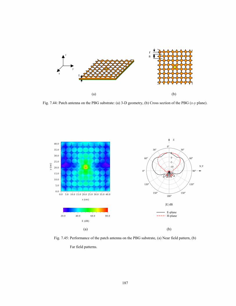
187
(a) (b)
Fig. 7.44: Patch antenna on the PBG substrate: (a) 3-D geometry, (b) Cross section of the PBG (x-y plane).
(a) (b)
Fig. 7.45: Performance of the patch antenna on the PBG substrate, (a) Near field pattern, (b)
Far field patterns.
r a
t
y
z
x
0.0 5.0 10.0 15.0 20.0 25.0 30.0 35.0 40.00.0
5.0
10.0
15.0
20.0
25.0
30.0
35.0
40.0
x (cm)
y (c
m)
20.0 40.0 60.0 80.0
E (dB)
5
0
-5
-10
0°30°
60°
90°
120°
150°180°
30°
60°
0°
120°
150°
|E| dB
Z
X,Y
E-plane H-plane

188
Fig. 7.46: Patch antenna on the effective dielectric substrate.
(a) (b)
Fig. 7.47: Performance of the patch antenna on the effective dielectric substrate, (a) Near field pattern, (b)
Far field patterns.
effective dielectric30.4=rε
original substrate 20.10=rε
0.0 5.0 10.0 15.0 20.0 25.0 30.0 35.0 40.00.0
5.0
10.0
15.0
20.0
25.0
30.0
35.0
40.0
x (cm)
y (c
m)
20.0 40.0 60.0 80.0
E (dB)
5
0
-5
-10
0°30°
60°
90°
120°
150°180°
30°
60°
0°
120°
150°
|E| dB
Z
X,Y
E-plane H-plane

189
7.3 Summary
The main objective of this chapter is to present the electromagnetic performance of the
periodic dielectric PBG structures and incorporate their unique propagation
characteristics into some potential applications as high Q nanocavity lasers, guiding the
EM waves at sharp bends, and miniaturized microstrip patch antennas.
The FDTD/Prony technique is successfully applied to obtain the broadband
characteristics of the triangular, rectangular, and woodpile PBG structures. It is observed
that the isolated dielectric regions create the TE ( zE ) band-gap while the connected
dielectric lattice produces the TM ( zH ) band-gap. A 3-D periodic composite material of
both isolated dielectrics and connected lattice has the potential to generate a complete
band-gap structure for all angles of arrival and for all polarization states, as appeared in
the novel woodpile PBG structure.
The possibility of modeling the dielectric PBG structures using the effective
dielectric media is also investigated. It is shown that, the effective periodic layered
dielectric material cannot model the performance of the PBG for large lattice constant
within the band-gap. For small lattice constants, outside the gap region, PBG and
effective medium have almost the similar behaviors.
A finite thickness 2-D PBG structure is presented to localize the EM waves in
three directions and design a high Q nanocavity laser. The periodic PBG structure forbids
the propagation of the defect excited mode (inside the band-gap) in the transverse plane,
and the total internal reflection traps the EM waves in the vertical direction. It is observed
that using a proper number of photonic cells and a suitable defect dielectric constant a

190
nanocavity laser with a relatively high quality factor (Q) can be designed. Also, it is
illustrated that the effective dielectric medium cannot model performance of the PBG in
designing the high Q cavity laser.
Potential application of the PBG structure for guiding the EM waves at sharp
bends namely, °90 and °60 corners is highlighted. To this end, an array of the PBG holes
in the guiding direction is removed. The guiding modes with their frequencies within the
gap-region are confined inside the channel, and they cannot be scattered through the
PBG. Additionally, a novel shaped bend, constructed using small holes at the corner, is
introduced to improve the coupling of the EM waves in the channels. Furthermore, it is
shown that the effective material is not able to model the PBG in turning the waves.
Designing the miniaturized microstrip patch antenna on the thick and high
dielectric substrate utilizing the PBG and effective dielectric materials for suppression of
the surface waves is also explored. It is demonstrated that although both dielectric PBG
and effective material cannot suppress the surface waves in all directions, but still they
have the advantage to reduce the surface waves and considerably improve the radiation
patterns of the miniaturized antenna. The mushroom EBG structure with the complete
surface wave band-gap region can be potentially useful to prevent the propagation of the
surface waves in all directions and design the miniaturized antenna with the higher
radiation characteristics and much more reduced edge diffraction effects.

191
Chapter 8
Composite Media with Negative Permittivity and Permeability Properties
The objective in this chapter is to characterize a novel structural configuration composed
of periodic array of conducting straight wires/Split Ring Resonators (SRR) that exhibits a
frequency range with simultaneously negative values of effective permittivity and
permeability [13]. This new class of material is called the Left-Handed (LH) medium and
has some unusual electromagnetic properties such as reversal of the Doppler shift,
anomalous refraction, and reversal of radiation pressure to radiation tension. These
behaviors can never be observed in naturally occurring materials or composites.
The FDTD/Prony technique is successfully applied to determine the
characteristics of this electromagnetic periodic structure. It is shown that a pass-band
occurs within the gap region of the composite medium where both permittivity and
permeability are negative; which it demonstrates the existence of the LH material. The
analysis methodology based on the FDTD technique is a capable engine to understand the
unique propagation behaviors of the LH media. The obtained results can be properly
integrated into some future potential applications of the composite LH materials.

192
8.1 Electromagnetic Properties of LH Materials
The concept of the LH materials is introduced by Veselago [84] in 1968. He theoretically
investigated the electrodynamics consequences of the medium having both negative
permittivity and permeability. Applying Maxwells equations in a LH material, the
electromagnetic plane waves are represented as
rkEE ⋅−= je0 (8.1a)
rkHH ⋅−= je0 (8.1b)
where kkk = , )()( ωεωµω effeffk = ( effµ and effε are the effective permeability and
permittivity of the material), and
⋅×= 00
)(EkH
ωωµeff
k (8.2)
It is determined from Eq. (8.2) that in the materials with negative effective
permittivity and permeability, ,, HE and k form a left-handed triplet of vectors ( )(ωµeff
has the negative sign in Eq. (8.2)). Thus, in the LH materials the energy flux
]Re[21 ∗×= HES is in the k− direction, and it flows in a direction opposite to the
plane wave propagation. Therefore, this new class of materials would have dramatically
different propagation characteristics compared to the ordinary or Right-Handed (RH)
materials. Some of the unique and potentially useful electrodynamics phenomena of the
LH materials such as (a) reversal of the Doppler shift, (b) anomalous refraction, and (c)
reversal of radiation pressure to radiation tension are briefed in the followings.

193
8.1.1 Reversal of the Doppler Shift
The group and phase velocities of the EM waves in an arbitrary medium are determined
using the energy flux and wave vectors, respectively. Thus, in a LH material the group
and phase velocities are in the opposite directions. Doppler shift in the RH/LH materials
for a detector moving with the velocity v in the presence of the source with the
frequency 0ω can be obtained as
⋅−=gvvs10ωω (8.3)
where s is the direction of the energy flux, gv is the group velocity, and ω is the
receiving frequency. The sign change of vs ⋅ in the right-/left-handed media, reveals the
reversal of the Doppler shift in the LH materials compared to the ordinary media.
8.1.2 Anomalous Refraction
Reflection and refraction behaviors of the EM waves at the boundary of the right/left-
handed media are demonstrated in this section. As mentioned earlier, in a right-handed
material both the wave vector k and energy flow S are in the same directions, while in the
left-handed material they are in the opposite directions. In addition, from the boundary
conditions between two different media 1 and 2
21 EnEn ×=× (8.4a)
21 HnHn ×=× (8.4b)
2211 EnEn ⋅=⋅ εε (8.4c)

194
, 2211 HnHn ⋅=⋅ µµ (8.4d)
it is readily obtained that, on the boundary between the right/left-handed media, the EM
fields have the same tangential components, while they have different normal
components in the opposite directions.
The above phenomena are applied to obtain the wave vector k, energy flux S, and
the E and H components of the incident, reflected, and refracted (transmitted) waves in
the RH and LH materials, as illustrated in Fig. 8.1.
Fig. 8.1: Reflection and refraction of the EM waves on the boundary between the
right/left-handed materials.
As observed, the refracted wave in the left-handed medium has the anomalous
behavior and it undergoes with the angle φ ( φθ sinsin 21 kk = ) with respect to the
normal to the boundary. The reflected wave is inside the right-handed medium and it has
the similar phenomena as the ordinary cases.
#1: right-handed material
n
ordinary
θ
θφφ
iE
rE
tEtH
rH
iH
iStS
rS
ik
rk
tk
#2: left-handed material

195
One of the useful applications of the above interesting phenomenon is presented
in Fig. 8.2. A flat slab LH material with large enough thickness and proper negative
permittivity and permeability has the potential to focus the point source radiation without
any reflection (parameters of the medium can be selected in a way to obtain the zero
reflection). This remarkably useful performance can never be achieved using the ordinary
materials.
(a) (b)
Fig. 8.2: The point source radiation, (a) is diverged by the flat slab RH material, and (b) is focused by
the flat slab LH material provided it is thick enough.
8.1.3 Reversal of Radiation Pressure to Radiation Tension
Another unusual behavior of the LH materials is reversal of the radiation pressure to
radiation tension. The electromagnetic momentum g related to the plane wave
propagating in the k direction is determined [84] as
kg ⋅=ωW (8.5)
where ω is the frequency and W is the total stored energy. As obseved, in a right-handed
material there is a pressure in the direction of propagation. However, in a left-handed
point source
l
d
EM waves are diverged
RH material
S
point source
l
d l-d EM waves are focused
LH material
S

196
material the vector k is directed toward the source of radiation and instead of pressure a
radiation tension or attraction is introduced.
These are some of the interesting features of the electrodynamic properties of the
LH materials. The task in the following section is to introduce a composite structural
configuration of conducting periodic elements with simultaneously negative permittivity
and permeability characteristics.
8.2 Characterization of LH Materials
In this section, a periodic array of conducting wires with negative permittivity is properly
combined with the split ring resonators with negative permeability to present the
composite material with simultaneously negative permittivity/permeability [13]. To
understand the physical behavior of the composite structure, the FDTD/Prony technique
is applied to characterize the straight wires, SRR, and straight wires/SRR. Fig. 8.3
pictorially represents the electromagnetic performances of the media having negative
effective permittivity, negative effective permeability, and both negative effective
permittivity/permeability, based on the definition of k vector ( kkk = ,
)()( ωεωµω effeffk = ).
8.2.1 Conducting Straight Wires
A 2-layer periodic array of conducting straight wires is presented in Fig. 8.4. The
reflected power for the normal and o30 oblique ( oo 150,90 == ii φθ ) incident plane

197
waves zE (TE case) is determined in Fig. 8.5. As observed, there is a single gap in the
propagation up to a cutoff frequency for modes with the electric field polarized along the
axis of the wires. The gap corresponds to a region where either )(ωε eff or )(ωµeff is
negative (decaying modes) (Fig. 8.3). Since the straight wires are excited by the electric
field, they cannot generate any effective permeability and the existence of the gap
indicates the presence of a negative effective permittivity.
8.2.2 Split Ring Resonators
The periodic array of split ring resonators has been recently introduced by Pendry et al.
[85] to extend the range of the electromagnetic properties of the effective media, and
present a novel material with effective magnetic permeability. It gives one the
opportunity to make a material with the negative permeability, from which a left-handed
medium can be constructed.
There are two incident polarizations of interest: magnetic field dominantly
polarized (a) along ( ||H ) and (b) perpendicular ( ⊥H ) to the axes of the rings. In both
cases the electric field is in the plane of the rings. Fig. 8.6 depicts the geometry of a 2-
layer periodic array of SRR for the ||H case. The applied plane wave induces the currents
that depending on the resonant properties of the structure produces a magnetic field,
which may either oppose or enhance the incident field. In particular, since the array of the
SRR is excited by the magnetic field polarized along the axes of the rings, the structure
has the potential to generate the effective permeability )(ωµ eff . The purpose of splitting

198
the rings is to generate a large capacitance in the small gap region between the rings in
order to concentrate the electric field and lower the resonance frequency.
The reflected power for both cases of normal and o30 oblique
( oo 150,90 == ii φθ ) plane waves (TE case) is presented in Fig. 8.7. The obtained
magnetic gap regions are based on the negative effective permeability of the material.
The performance of the SRR for the ⊥H case (Fig. 8.8) is also studied, and the incident
reflected power is determined in Fig. 8.9. In this case, the magnetic effects are small, and
the )(ωµ eff is small, positive, and slowly varying. The negative effective permittivity of
the structure generates the dielectric gap regions.
8.2.3 Conducting Straight Wires/Split Ring Resonators
To present a LH material, the straight wires are combined with the SRR for the ||H case,
as shown in Fig. 8.10. The characteristics of the composite structure for the normal and
oblique incident waves are presented in Fig. 8.11. It is clearly illustrated in Fig. 8.12 that
around the frequency GHz3.5 , a pass-band occurs within the previously forbidden gaps
of both the conducting wires and SRR. This indicates that the negative )(ωε eff of the
straight wires is combined with the negative )(ωµ eff of SRR to allow the propagation,
and present the novel composite material with negative permittivity/permeability.
This performance can be compared with the behavior of the composite material of
straight wires/SRR for the ⊥H case (Fig. 8.13), as determined in Fig. 8.14. As observed,
in this case, a small pass-band is obtained which is within a narrow range that ends

199
abruptly at the band edge of the lowest dielectric gap of the SRR. The pass-band occurs
where the effective dielectric of the SRR exceeds the negative dielectric of the medium of
wires (positive permittivity/permeability). The contrast between the propagation bands of
||H and ⊥H cases, demonstrates the difference between the performances of SRR ( ||H )
with negative permeability compared to the SRR ( ⊥H ) with negative permittivity. Note
that the observations are very similar compared to the data presented in [13] utilizing
dispersion diagram.
(a)
(b)
(c)
Fig. 8.3: Electromagnetic performances of the media having (a) negative effective permittivity, (b) negative
effective permeability, and (c) both negative effective permittivity/permeability.
EM wave cannot get through at the
band-gap frequencies
negative effective εeff(ω)
plane wave
EM wave cannot get through at the
band-gap frequencies
negative effective µeff(ω)
plane wave
EM wave can get through at theband-gap frequencies of
negative εeff(ω) and negative µeff(ω) materials (pass-band)
negative effective εeff(ω)/µeff(ω)
plane wave

200
Fig. 8.4: 2-Layer conducting straight wires: (a) Periodic structure, (b) Unit cell of the structure. Note that
the PBC walls are positioned on the PEC edges.
Fig. 8.5: Normal and o30 oblique incidence reflected power of the straight wires. Negative effective
permittivity of the structure creates the dielectric gap region.
(b) (a)
y
z
x
mmTmmrw
880.0
==
T
T
T
rw
0.0 5.0 10.0 15.0 20.0 25.0 30.0frequency (GHz)
0.0
20.0
40.0
60.0
80.0
100.0
120.0
% of
Powe
r Refl
ected
normal incidence30
o oblique incidence

201
Fig. 8.6: 2-Layer split ring resonators ( ||H ): (a) Periodic structure, (b) Unit cell of the structure.
Fig. 8.7: Normal and o30 oblique incidence reflected power of the SRR ( ||H ). Negative effective
permeability of the structure creates the magnetic gap regions.
0.0 5.0 10.0 15.0 20.0 25.0 30.0frequency (GHz)
0.0
20.0
40.0
60.0
80.0
100.0
120.0
% of
Powe
r Refl
ected
normal incidence30
o oblique incidence
(b) (a)
y
z
x
mmTmmcmmbmmammrr
840.020.080.060.1
=====
T
T
T
rr
a
b
c

202
Fig. 8.8: 2-Layer split ring resonators ( ⊥H -same dimensions as ||H case): (a) Periodic
structure, (b) Unit cell of the structure.
Fig. 8.9: Normal and o30 oblique incidence reflected power of the SRR ( ⊥H ). Negative effective
permittivity of the structure creates the dielectric gap regions.
0.0 5.0 10.0 15.0 20.0 25.0 30.0frequency (GHz)
0.0
20.0
40.0
60.0
80.0
100.0
120.0
% of
Powe
r Refl
ected
normal incidence30
o oblique incidence
(b) (a)
y
z
x
mmT 8=
T
T
T

203
Fig. 8.10: Composite material of 2-layer straight wires/split ring resonators ( ||H ): (a) Periodic structure,
(b) Unit cell of the structure. Note that the PBC walls are positioned on the PEC edges.
Fig. 8.11: Normal and o30 oblique incidence reflected power of the straight wires/SRR ( ||H ). Negative
effective permittivity of the straight wires are combined with the negative effective permeability
of the SRR ( ||H ) to present the LH material around the frequency GHz3.5 (pass-band region).
(b) (a)
y
z
x
mmT 8=
T
T
T
T/2
0.0 5.0 10.0 15.0 20.0 25.0 30.0frequency (GHz)
0.0
20.0
40.0
60.0
80.0
100.0
120.0
% of
Powe
r Refl
ected
normal incidence30
o oblique incidence

204
Fig. 8.12: Illustration of the LH material with negative permittivity/permeability. The pass-band occurs
within the dielectric/magnetic gap regions of the straight wires/SRR.
4.6 4.8 5.0 5.2 5.4 5.6 5.8 6.0frequency (GHz)
0.0
20.0
40.0
60.0
80.0
100.0
120.0
% of
Powe
r Refl
ected
straight wiresSRRstraight wires/SRR
Negative µ
Negative ε
LH Material

205
Fig. 8.13: Composite material of 2-layer straight wires/split ring resonators ( ⊥H ): (a) Periodic structure,
(b) Unit cell of the structure. Note that the PBC walls are positioned on the PEC edges.
Fig. 8.14: Normal and o30 oblique incidence reflected power of the straight wires/SRR ( ⊥H ). The SRR
( ⊥H ) has the positive permeability and no LH property can be achieved. Notice that the pass-
band occurs where the composite material has the positive effective permittivity/permeability.
(b) (a)
y
z
x
mmT 8=
T
T
T
T/2
0.0 5.0 10.0 15.0 20.0 25.0 30.0frequency (GHz)
0.0
20.0
40.0
60.0
80.0
100.0
120.0
% of
Powe
r Refl
ected
normal incidence30
o oblique incidence

206
8.3 Summary and Future Investigations
In this chapter, a novel composite material of periodic conducting straight wires/split ring
resonators is presented to introduce a LH material with simultaneously negative
permittivity and permeability. The powerful FDTD/Prony technique is successfully
applied to characterize and demonstrate the unique electromagnetics phenomena of the
complex structure. It is illustrated that the straight wires with negative permittivity are
properly combined with the split rings with negative permeability to design a composite
material with negative permittivity/permeability.
The results presented in this work, are the basis for further investigations of the
fascinating electrodynamics effects anticipated for such composite material in order to
incorporate these into some potential applications.

207
Chapter 9
Summary and Suggestions for Future Work
9.1 Summary
The main objectives of the work described in this dissertation are to characterize the
electromagnetic performances of two classes of composite structures, namely, (a) multi-
layered complex media, and (b) periodic Electromagnetic Band-Gap (EBG) structures;
and to incorporate their unique propagation characteristics into some novel applications.
The advanced and diversified computational techniques are developed to effectively
analyze the interaction of the structures with electromagnetic waves. The key
achievements of this research may be summarized as
Vector Wave Solution/GA Technique: The vector wave solution of Maxwells equations
is integrated with the genetic algorithm to obtain a capable technique for characterizing
multi-layered complex media and presenting their novel optimized designs.
RCS Reduction of Canonical Targets: The modal solution/GA technique is applied to
determine the optimal composite coatings for RCS reduction of canonical targets in a
wide-band of frequency range. Both monostatic and bistatic cases are studied. A Hybrid

208
GA with planar/curved surface implementation is also introduced to efficiently reduce the
RCS of the curved structures.
Non-Uniform Luneburg and 2-Shell Lens Antennas: Design optimization of the non-
uniform Luneburg lens antenna is successfully obtained utilizing the vector wave solution
of Maxwells equations integrated with the GA/adaptive-cost-function. Additionally, a
novel 2-shell lens antenna with high performance radiation characteristics is presented.
Many useful engineering guidelines are highlighted.
FDTD Analysis of Complex Periodic Structures: A powerful computational engine
utilizing FDTD technique with PBC/PML boundary conditions is developed to accurately
determine the broadband electromagnetic characteristics of the complex periodic EBG
structures. The Prony extrapolation scheme is also integrated to increase the efficiency of
the presented method.
Frequency Selective Surfaces: The FDTD/Prony technique is successfully applied to
characterize different classes of challenging FSS such as, (a) double concentric square
loop FSS, (b) dipole FSS manifesting high Q resonance, (c) patch FSS manifesting high
Q resonance, (d) crossed dipole FSS, (e) dichroic plate FSS, (f) inset self-similar aperture
FSS, (g) fractal FSS, (h) multi-layered tripod FSS, (i) 9-layer dielectric/inductive square
loop FSS, and (j) smart surface mushroom FSS. The results are extremely satisfactory
demonstrating the capability of the developed engine.

209
Photonic Band-Gap Materials: To understand the performance of the PBG/periodic
dielectric materials, the FDTD/Prony technique is applied to present their innovative
propagation characteristics. The band-gap phenomena of the triangular, rectangular, and
woodpile PBG are effectively investigated. The results are integrated into the three
potential applications, namely, high Q nanocavity lasers, guiding the EM waves in sharp
bends, and miniaturized microstrip patch antennas. A comparative study with the
effective dielectric materials is also provided.
Composite LH Media: A composite material of two periodic conducting structures,
straight wires with negative effective permittivity/split ring resonators with negative
effective permeability, is presented to generate a new medium with both negative
permittivity/permeability. The structure has the unique electrodynamic properties, and is
successfully characterized utilizing the FDTD/Prony technique.
9.2 Suggestions for Future Work
It is demonstrated that the computational engines presented in this dissertation are very
capable in characterizing complex layered and periodic band-gap structures. However, it
is believed that the number of new ideas is endless. The followings are a few suggestions
for future work.
• In this work, to efficiently reduce the RCS of curved structures, a GA with hybrid
planar/curved surface implementation is introduced. The hybrid GA is
successfully applied to determine the optimal coating for a canonical spherical

210
structure. Although, the obtained lossy RAM coating can be also applied to
reduce the RCS of curved/non-canonical structures; however, one may extend the
developed method to directly integrate the hybrid GA with a numerical technique
analyzing surfaces with arbitrary curvatures, to effectively present their optimal
coatings.
• To present the optimal design for some applications of interest, one needs to
determine the tradeoffs between a set of conflict goals. The GA with adaptive cost
function, as applied in this work, has the potential to properly obtain the best
tradeoffs. However, finding a suitable algebraic combination of goals for use as
an adaptive objective function may be a difficult task. The Pareto GAs avoid this
problem by returning not a single optimal design, but the set of designs that
represents all of the best tradeoffs [20]. This can be achieved by modifying the
genetic algorithm, described in this work, to allow the population to converge
toward the whole Pareto front instead of a subset of that.
• The FDTD/Prony technique, as demonstrated in this dissertation, is a highly
successful solution to a wide variety of electromagnetic wave interaction
problems. However, the developed method is restricted to the orthogonal grids,
and the structure boundaries that do not conform to the orthogonal coordinate
must be approximated using staircasing. The Nonorthogonal FDTD (N-FDTD)
scheme based on the global curvilinear coordinate system [9] is an effective
approach to accurately analyze these structures. In addition, to improve the

211
efficiency of the technique, one may enmesh the FDTD domain using the
nonuniform grids [9]. Thus, the next challenge for this work could be the
implementation of a very capable computational engine utilizing N-
FDTD/nonuniform grids integrated with the Prony method to accurately and
efficiently obtain the EM performance of the structures with complex boundaries.
• The characteristics of different classes of challenging periodic electromagnetic
band-gap structures are presented in this research. However, the key engineering
question is, how one can present the best optimal design for the application of
interest? To answer this question, our FDTD/Prony engine has to be integrated
with a capable optimization method. The optimizer could be the genetic
algorithm, or a local technique such as conjugate-gradient or quasi-Newton
method. The main considerations are (a) to properly choose the objective
function, and (b) to efficiently integrate the FDTD with the optimization
technique. The FDTD/optimization method has a tremendous advantage in
presenting new structural configurations for frequency selective surfaces,
photonic band-gap materials, etc.
• The performance of the novel LH composite material, presented in this work,
demonstrates that the frequency bandwidth of the region with negative
permittivity/permeability and the level of reflection coefficient in this region, are
the important issues that need to be studied in greater depth. Further work is
required to investigate a more applicable structure with improved characteristics

212
and simple fabrication. The unique electrodynamic properties of the LH media
can be integrated into the future potential designs.

213
Appendix A
Electromagnetic Scattering from an Arbitrary Configuration of Eccentric Spheres
A.1 Objective
In this appendix the formulation for the scattering of the electromagnetic waves from an
arbitrary configuration of eccentric spheres is presented. The modal solution of Maxwells
equations in the coordinate of each sphere is represented using the spherical vector wave
functions. Next, the Greens second theorem is used to impose the boundary conditions on
the spherical interfaces. Additional theorems in the spherical coordinates are also applied to
express the M and N wave functions in one coordinate system in terms of the wave
functions in another coordinate system. Utilizing this transformation and by employing the
orthogonality of the spherical wave functions, one can obtain the matrix equations, and
then the scattered fields.

214
A.2 Modal Solution of Eccentric Spherical Structures
Fig. A.1 depicts a configuration of N eccentric spheres illuminated by an arbitrary incident
plane wave. The EM fields in the ith region and spherical coordinate oj can be expressed
utilizing the spherical vector wave functions (Chapter 2) in the following form
Fig. A.1: Configuration of N eccentric spheres and their corresponding coordinates.
∑ ⋅=mn
jiT
mnnmii k,
,, ),()( rWCrE (A.1)
where
( )nminminminminmi dcba ,,,,, =C (A.2a)
( )⋅= ),(),(),(),(),( )4(,
)1(,
)4(,
)1(,, jimnjimnjimnjimnjimn kkkkk rNrNrMrMrW (A.2b)
i eincident field
k1
o1
x
y
z oj
oN
oi
o2
k
kN
k2
kj
ki
1r1r′
11 rr ′−
ij0r
irV

215
In region 1, the EM fields are the combination of both incident and scattered fields. For
the incident field propagating in the i direction with the polarization along the e , a
representation in the spherical coordinate 1o can be obtained as
⋅⋅=∑mn
Tmn
inm
i k,
11,,11 ),()( rWCrE (A.3)
The unknown coefficient inm,1C is
( )00 ,1,1,1i
nmi
nmi
nm ca=C (A.4)
where [15]
( )iimn
mni
nm enn
nja φθ ,)1(
)12()1(,,1 −
−
⋅+
+−= R (A.5a)
( )iimn
mni
nm enn
njc φθ ,)1(
)12()1(,
11
,1 −
+−−
⋅+
+−= S (A.5b)
and
( )
−
+=
θθφθ
θθφθ φ
ddPPjme
nn
mnm
njm
mn)(cos)(cos
sin
)1(1,,R (A.6a)
( ) ⋅
+
+= )(cos
sin)(cos
)1(1,, θ
θφ
θθθφθ φ m
n
mnjm
mn Pjmd
dPenn
S (A.6b)
Thus, the total field in region 1 and coordinate o1 is simply determined using the Eq. (A.1)
with coefficient
( ) ⋅= nmi
nmnmi
nmnm dcba ,1,1,1,1,1C (A.7)
The scattered fields in regions Ni ,,3,2 L= is obtained using Eq. (A.1) with
( ) ⋅= 00 ,,, nminminmi caC (A.8)

216
A.3 Boundary Conditions
A.3.1 Dyadic Greens Second Theorem
Boundary conditions on the spherical interfaces are imposed using the dyadic Greens
second theorem in the region between the spheres with propagation constant k
[ ] =′⋅×∇ ′×∇ ′−×∇ ′×∇ ′⋅∫ vdV
QPQP )(
[ ] ⋅′×∇ ′⋅×′+⋅×∇ ′×′− ∫ sdnnS
QPQP )()( (A.9)
Taking
HP = (A.10a)
IGQ ),(11),( 2 rrGk
rr ′
⋅∇ ′∇ ′+=′= ,
rrerrG
rrjk
′−=′
′−−
),( (A.10b)
one can obtain for Vr ∉
⋅=′⋅×′×+′⋅×′×∇×≡ ∫∫ SSsdjsd 0)()()( GEnnGHnnrL ωε (A.11)
The dyadic Greens function ),( rr ′G can be expressed in terms of spherical wave
functions M and N as
[ ]∑ ><−><− +++−−=′
mnmnmnmnmn
m
nnnjkrr
,
)4(,
)1(,
)4(,
)1(, )()()()(
)1(12)1(),( rNrNrMrMG (A.12)
where > or < means that the spherical variables ),,( φθr are defined in the coordinate r or
r ′ based on the ),( rrMax ′ or ),( rrMin ′ , respectively. By substituting Eq. (A.12) in Eq.
(A.11), the following equations for iSr ∈ ( Ni ,,2,1 L= ) are attained [86]

217
:rr ′>
+
Ω′⋅×′+
+−−× ∑ ∫ −mn
S mnnmnm dkrjk
nnnkrj
,,
)4(,
2 )()(),()1(
12)1()( RHnrNn
+Ω′⋅×′+Ω′⋅×′ ∫∫ −− S mnnmnS mn
dn
mn dkrjkjdkr
krjk ,)4(
,,)4(
, )()(),()()(
),( REnrMSHnrMη
0)()(
),( ,)4(
, =
Ω′⋅×′∫ −S mn
dn
mn dkr
krjkj SEnrN
η (A.13a)
:rr ′<
+
Ω′⋅×′+
+−−× ∑ ∫ −mn
S mnnmnm dkrhk
nnnkrj
,,
)2()1(,
2 )()(),()1(
12)1()( RHnrNn
+Ω′⋅×′+Ω′⋅×′ ∫∫ −− S mnnmnS mn
dn
mn dkrhkjdkr
krhk ,)2()1(
,,
)2()1(, )()(),()(
)(),( REnrMSHnrM
η
0)()(
),( ,
)2()1(, =
Ω′⋅×′∫ −S mn
dn
mn dkr
krhkj SEnrN
η (A.13b)
where Ω′d is the solid angle of sphere. Notice that ( )′≡ )()( xxzxz ndn , where nz could be
spherical Bessel or second order spherical Hankel functions; and
),()()1(),( ,)1(, φθmnnmn krjnnk SrMr +=× (A.14a)
),()()1(),( ,)2()4(
, φθmnnmn krhnnk SrMr +=× (A.14b)
),()(
)1(),( ,)1(, φθmn
dn
mn krkrjnnk RrNr +−=× (A.14c)

218
⋅+−=× ),()(
)1(),( ,
)2()4(
, φθmn
dn
mn krkrhnnk RrNr (A.14d)
Using Eq. (A.13), continuity of En ×′ and Hn ×′ on the spherical boundaries, and the
orthogonality between mn,R and mn,S , it is obtained that
:,,2,1, NjSr j L=∈
+×
+−∑ ),()(
)()()( 1
)1(,
,11
)2(
1
1)2(
11
11)2(
1)2(
1,1
21 rkrkh
krkrhj
rkrkh
krhjbr mnjmn
n
dn
dn
nnm Nrηη
+×
− ),()(
)()()(
1)1(,
11
11)2(
1)2(
11)2(
1
1)2(
1,1 rk
rkrkh
krhjrkhkr
krhjd mnj
dn
nn
dn
nm Mrηη
+×
−∑∑
=
),()()()(
)( )4(,
,,
2
2imnj
mniin
i
idn
ii
iidn
ini
nmi
N
ii krkj
krkrjj
rkrkj
krjjar rNrηη
=×
+− ),()(
)()()( )4(
,, imnjii
iidn
iniini
idn
inmi k
rkrkj
krjjrkjkr
krjjc rMrηη
+×
+−− ∑ ),()(
)()()( 1
)1(,
,11
1
1)2(
11
111
)2(
1,1
21 rNr krkj
krkrhj
rkrkj
krhjar mnjmn
n
dn
dn
ni
nm ηη
⋅×
− ),()(
)()()(
1)1(,
11
111
)2(11
1
1)2(
1,1 rMr k
rkrkj
krhjrkjkr
krhjc mnj
dn
nn
dni
nm ηη (A.15)

219
A.3.2 Spherical Translational Additional Theorems
To apply the orthogonality of the spherical vector wave functions and obtain the matrix
equations, one needs to express the spherical functions M and N in one coordinate system
in terms of the spherical functions in another coordinate system, based on the translational
additional theorems in spherical coordinates [87], [88]. After some mathematical
manipulations, it is determined that
( )∑ +=µν
µννµµννµ,
,,
,,
, ),(),(),( jijnm
jijnm
imn kBkAk rNrMrM (A.16a)
( )∑ +=µν
µννµµννµ,
,,
,,
, ),(),(),( jijnm
jijnm
imn kBkAk rMrNrN (A.16b)
where
∑ −−−−=p
mjijmp
ijp
ijnm ij
ePkrzpvnapmnaA 0)(00
, )(cos)(),,(),,,,()1( φµµµνµ θµν (A.17a)
∑ −−−−−=p
mjijmp
ijp
ijnm ij
ePkrzpvnbppmnaB 0)(00
, )(cos)(),,()1,,,,,()1( φµµµνµ θµν (A.17b)
[ −−+++−++++= −+ ))(1)(1()12)(1(2),,( pnpnjpna np ννννννν ν
] ))1(2()2)(1( ++++++− ννννν pnpn (A.17c)
[ ] ⋅+−+−+−++++= −+ 21))()(1)(1(),,( pnpnpnpnjpnb np ννννν ν
))1(2()12( ++ ννν (A.17d)
⋅
++−−−−+++−= +
21
)!()!()!()!()!()!()12()1(),,,,(
µµνµµνµν µ
mpmnmpmnppmna m
−−
µµ
ννmm
pnpn000
(A.17e)

220
⋅
++−−−−+++−= +
21
)!()!()!()!()!()!()12()1(),,,,,(
µµνµµνµν µ
mpmnmpmnpqpmna m
−−
µµ
ννmm
pnqn000
(A.17f)
321
321
llljjj
is the Wigner 3-j symbol, and ),,( 000ijijijr φθ is the spherical coordinate of
the position vector jo with respect to the coordinate io .
A.3.3 Matrix Equations
Substituting Eq. (A.16) into the Eq. (A.15), and using the orthogonal properties of the
spherical function, the following matrix equations are obtained
:,,2,1, NjSr j L=∈
I)
+
−∑ nm
mnn
dn
dnn
j
jnmj
d brkhkrhk
rkhkrhkr
rAkrj ,1,
11)2(
1)2(
11)2(
1)2(
11
11, )()(1)()(1)(ηηνµν
+
+− nm
dnnn
dn
j
jnm drkhkrhk
rkhkrhkr
rB ,111)2(
1)2(
111
)2(1
)2(
1
11, )()(1)()(1ηηνµ
+
+−∑∑
=nmi
N
i mniini
dnii
dnin
iij
iijnmj
d arkjkrjk
rkjkrjkr
rAkrh ,
2 ,
,)2( )()(1)()(1)(ηηνµν
=
− nmiii
dnin
iiini
dn
ij
iijnm crkjkrjk
rkjkrjkr
rB ,
, )()(1)()(1ηηνµ

221
+
−− ∑ i
nmmn
nd
ndnn
j
jnmj
d arkjkrhk
rkjkrhkr
rAkrj ,1,
111)2(
111)2(
11
11, )()(1)()(1)(ηηνµν
inm
dnnn
dn
j
jnm crkjkrhk
rkjkrhkr
rB ,1111)2(
1111
)2(
1
11, )()(1)()(1
+−
ηηνµ (A.18a)
II)
+
+−∑ nm
mnn
dn
dnn
jnmjv brkhkrh
krkhkrh
krBkrj ,1
,11
)2(1
)2(11
)2(1
)2(
111
1, )()(1)()(1)(ηηνµ
+
− nm
dnnn
dn
jnm drkhkrhk
rkhkrhk
rA ,111)2(
1)2(
111
)2(1
)2(
11
1, )()(1)()(1ηηνµ
+
−∑∑
=nmi
N
i mniini
dnii
dnin
iii
ijnmj arkjkrj
krkjkrj
krBkrh ,
2 ,
,)2( )()(1)()(1)(ηηνµν
=
+− nmiii
dnin
iiini
dn
ii
ijnm crkjkrjk
rkjkrjk
rA ,, )()(1)()(1
ηηνµ
+
+−− ∑ i
nmmn
nd
ndnn
jnmjv arkjkrh
krkjkrh
krBkrj ,1
,111
)2(111
)2(
111
1, )()(1)()(1)(ηηνµ
⋅
− i
nmdnnn
dn
jnm crkjkrhk
rkjkrhk
rA ,1111)2(
1111
)2(
11
1, )()(1)()(1ηηνµ (A.18b)
This set of matrix equations can be successfully solved to determine the unknown
coefficients ,,, ,,1,1 nminmnm adb and nmic , ( Ni ,,3,2 L= ); and then compute the scattered
electromagnetic fields from the eccentric spheres.

222
Appendix B
FDTD/Prony for Efficient Analysis of Complex Periodic Structures
As mentioned earlier, the periodic structures require extensive simulation time due to the
multiple reflections, which occur in setting up the modal distribution on the periodic
body. Thus, the simulation involves many time steps, which is time consuming and it
increases the numerical errors over the long period of time. The periodic structures can be
efficiently analyzed utilizing the Pronys scheme.
To this end, the FDTD technique is run long enough to allow a sufficient time for
settling the initial transient and developing the time harmonic fields. Next, the Pronys
method is applied to effectively extrapolate the truncated time domain results. Based on
our experience, to achieve the accurate results, one needs to allow the process of the
time-stepping algorithm for about ten-fifteen round trips propagation of the scattered
waves between the ABC walls.
Fig. B.1 shows a double concentric square loop FSS. The structure is analyzed
utilizing the FDTD and FDTD/Prony techniques; and the results for the scattered fields in
time and frequency domains are determined in Figs. B.2 and B.3. To accurately
characterize the structure using the FDTD technique, one needs about 28 cycles (round

223
trips) time analysis between the ABC walls, which it takes around 155 min. on an HPC-
180 workstation.
To properly apply the Pronys method, the FDTD technique is run for about ten
cycles (55 min.) including of 2124 iterations, as shown in Fig. B.2. A window of 600
iterations is sampled at every 12 iterations to obtain 50 data points from which the
complex exponential functions and unknown coefficients are found by applying the
Pronys method. After experimenting a few times by shifting the window up and down
on the FDTD records, it is obtained that a 5-terms series of exponential functions
satisfactorily fits the FDTD data with mean square error 610−=χ [89]. The scattered
field, as demonstrated in Figs. B.2 and B.3, is accurately and efficiently obtained utilizing
the FDTD/Prony in about 55.04 min. Notice that the FDTD with ten cycles propagating
waves between the ABC walls cannot generate the accurate results, as illustrated in Fig.
B.3.
Fig. B.1: Double concentric square loop FSS: (a) Periodic structure, (b) Unit cell of the structure.
(b) (a)
TWTW
TdTt
6875.0875.0
1616
2
1
==
==
T
W2
W1
d
d
T
t
y
z
x

224
Fig. B.2: Normal incidence scattered field of the double concentric square loop FSS in the time
domain. A comparative study between FDTD and FDTD/Prony.
Fig. B.3: Normal incidence reflected power of the double concentric square loop FSS in the frequency
domain. A comparative study between FDTD and FDTD/Prony.
0.20 0.25 0.30 0.35 0.40T/λ
0.0
20.0
40.0
60.0
80.0
100.0
120.0
% of
Powe
r Refl
ected
FDTD (28−cycle): 155 min.FDTD (10−cycle): 55 min.FDTD/Prony (10−cycle): 55.04 min.
0.0 100.0 200.0 300.0 400.0 500.0Time Steps (*12)
0.0
0.1
0.2
0.3
0.4
0.5
0.6
0.7
0.8
0.9
1.0
Scatt
ered F
ield
FDTD (28−cycle): 155 min.FDTD (10−cycle): 55 min.FDTD/Prony (10−cycle): 55.04 min.
Pronys extrapolation region

225
Bibliography
[1] J. R. Wait, Electromagnetic Waves in Stratified Media, IEEE Press, NY, 1996. [2] J. R. Wait, Electromagnetic Radiation from Cylindrical Structures, IEE Press,
London, 1988. [3] C. T. Tai, Dyadic Greens Functions in Electromagnetic Theory, IEEE Press, NY,
1994. [4] Y. Rahmat-Samii and E. Michielssen, Electromagnetic Optimization by Genetic
Algorithms, John Wiley and Sons, NY, 1999. [5] H. C. Strifors and G. C. Gaunaurd, Scattering of electromagnetic pulses by simple-
shaped targets with radar cross section modified by a dielectric coating, IEEE Trans. Antennas Propagat., vol. 46, no. 9, pp. 1252-1262, Sept. 1998.
[6] H. Shrank and J. R. Sanford, A Luneburg-lens update, IEEE Antennas Propagat.
Mag., vol. 37, no.1, pp. 76-79, Feb. 1995. [7] Y. Rahmat-Samii and H. Mosallaei, Electromagnetic band-gap structures:
Classification, characterization, and applications, 11th International Conference on Antennas and Propagation, UMIST, Manchester, UK, Apr. 17-20, 2001.
[8] A. Taflove, Computational Electrodynamics: The Finite-Difference Time-Domain
Method, Artech House, MA, 1995. [9] A. Taflove, Advances in Computational Electrodynamics: The Finite-Difference
Time-Domain Method, Artech House, MA, 1998. [10] T. K. Wu, Frequency Selective Surface and Grid Array, John Wiley & Sons, NY,
1995. [11] B. A. Munk, Frequency Selective Surfaces: Theory and Design, John Wiley & Sons,
NY, 2000.

226
[12] J. D. Joannopoulos, R. D. Meade, and J. N. Winn, Photonic Crystals: Molding the Flow of Light, Princeton University Press, NJ, 1995.
[13] D. R. Smith, W. J. Padilla, D. C. Vier, S. C. Nemat-Nasser, and S. Schultz,
Composite medium with simultaneously negative permeability and permittivity, Phys. Rev. Lett., vol. 84, no. 18, pp. 4184-4187, May 2000.
[14] W. C. Chew, Waves and Fields in Inhomogeneous Media, IEEE Press, NY, 1995. [15] N. C. Skaropoulos, M. P. Ioannidou, and D. P. Chrissoulidis, Indirect mode-
matching solution to scattering from a dielectric sphere with an eccentric inclusion, Opt. Soc. Amer., vol. 11, no. 6, pp. 1859-1866, June 1994.
[16] M. Abramowitz and I. A. Stegun, Handbook of Mathematical Functions with
Formulas, Graphs, and Mathematical Tables, Dover Publications, 1972. [17] D. E. Amos, A Subroutine Package for Bessel and Hankel Functions of Complex
Arguments, Sandia National Laboratories, CA, 1996. [18] D. J. Hoppe and Y. Rahmat-Samii, Impedance Boundary Conditions in
Electromagnetics, Taylor & Francis Publications, 1995. [19] J. M. Johnson and Y. Rahmat-Samii, Genetic algorithms in engineering
electromagnetics, IEEE Antennas Propagat. Mag., vol. 39, no. 4, pp. 7-21, Aug. 1997.
[20] D. S. Weile and E. Michielssen, Genetic algorithm optimization applied to
electromagnetics: A review, IEEE Trans. Antennas Propagat., vol. 45, no. 3, pp. 343-353, Mar. 1997.
[21] D. L. Carroll, Fortran Genetic Algorithm Driver, University of Illinois at Urbana-
Champaign, 1997. [22] E. Michielssen, J. M. Sajer, S. Ranjithan, and R. Mittra, Design of lightweight,
broad-band microwave absorbers using genetic algorithms, IEEE Trans. Microwave Theory Tech., vol. 41, no. 6/7, pp. 1024-1031, June/July 1993.
[23] D. S. Weile, E. Michielssen, and D. E. Goldberg, Genetic algorithm design of
Pareto optimal broad-band microwave absorbers, IEEE Trans. Electromagnetic Compatibility, vol. 38, no. 3, pp. 518-524, Aug. 1996.
[24] B. Chambers and A. Tennant, Optimized design of Gaumann radar absorbing
materials using a genetic algorithm, IEE Proceedings on Radar, Sonar and Navigation, vol. 143, no. 1, pp. 23-30, Feb. 1996.

227
[25] R. E. Hiatt, K. M. Siegel, and H. Weil, The ineffectiveness of absorbing coatings on conducting objects illuminated by long wavelength radar, Proc. IRE, vol. 48, pp. 1636-1642, Sept. 1960.
[26] A. Ishimaru, Electromagnetic Wave Propagation, Radiation, and Scattering,
Prentice-Hall, NJ, 1991. [27] C. S. Silitonga, Y. Sugano, H. Sakura, M. Ohki, and S. Kozaki, Optimum variation
of the Luneburg lens for electromagnetic scattering calculations, Int. J. Electronics, vol. 84, no. 6, pp. 625-633, June 1998.
[28] J. R. Sanford, Scattering by spherically stratified microwave lens antennas, IEEE
Trans. Antennas Propagat., vol. 42, no. 5, pp. 690-698, May 1994. [29] M. A. Mitchell and J. R. Sanford, Luneburg lens revival, Electronics and Wireless
World, vol. 95, no. 1639, pp. 456-458, May 1989. [30] K. W. Kim and Y. Rahmat-Samii, Spherical Luneburg lens antennas: Engineering
characterizations including air gap effects, 1998 IEEE AP-S International Symposium, pp. 2062-2065, Atlanta, GA, June 21-26, 1998.
[31] R. K. Luneburg, Mathematical Theory of Optics, University of California Press, CA,
1964. [32] S. Cornbleet, Microwave and Optical Ray Geometry, John Wiley & Sons, NY, 1984. [33] R. S. Elliott, Antenna Theory and Design, Prentice-Hall, NJ, 1981. [34] S. M. Morgan, Generalization of spherically symmetric lenses, IRE Trans.
Antennas and propagat., vol. 7, no. 4, pp. 342-345, Oct. 1959. [35] J. S. Hollis and M. W. Long, A Luneburg lens scanning system, IRE Trans.
Antennas and Propagat., vol. 5, no. 1, pp. 21-25, Jan. 1957. [36] E. F. Buckley, Stepped-index Luneburg lenses, Electronic Design, pp. 86-89, Apr.
1960. [37] L. C. Gunderson and G. T. Holmes, Microwave Luneburg lens, Applied Optics,
vol. 7, no. 5, pp. 801-804, May 1968. [38] T. L. Ap-Rhys, The design of radially symmetric lenses, IEEE Trans. Antennas
Propagat., vol. 18, no. 4, pp. 497-506, July 1970.

228
[39] H. M. Nussenzveig, Complex angular momentum theory of the rainbow and the glory, J. Opt. Soc. Am., vol. 69, no. 8, pp. 1068-1079, Aug. 1979.
[40] R. Mittra, C. H. Chan, and T. Cwik, Techniques for analyzing frequency selective
surface-a review, Proc. IEEE, vol. 76, no. 12, pp. 1593-1615, Dec. 1988. [41] P. Harms, R. Mittra, and W. Ko, Implementation of the periodic boundary
condition in the finite-difference time-domain algorithm for FSS structures, IEEE Trans. Antennas Propagat., vol. 42, no. 9, pp. 1317-1324, Sept. 1994.
[42] J. A. Roden, S. D. Gedney, M. P. Kesler, J. G. Maloney, and P. H. Harms, Time-
domain analysis of periodic structures at oblique incidence: Orthogonal and nonorthogonal FDTD implementations, IEEE Trans. Microwave Theory Tech., vol. 46, no. 4, pp. 420-427, Apr. 1998.
[43] J.-P. Berenger, Three-dimensional perfectly matched layer for the absorption of
electro-magnetic waves, Journal of Computational Physics, vol. 127, no. 2, pp. 363-379, Sept. 1996.
[44] W. L. Ko and R. Mittra, A combination of FD-TD and Pronys methods for
analyzing microwave integrated circuits, IEEE Trans. Microwave Theory Tech., vol. 39, no. 12, pp. 2176-2181, Dec. 1991.
[45] E. A. Parker, S. M. A. Hamdy, R. J. Langley, Modes of resonance of the Jerusalem
cross in frequency-selective surfaces, IEE Proc., pt. H, vol. 130, no. 3, pp. 203-208, Apr. 1983.
[46] T. A. Cwik and R. Mittra, Scattering from a periodic array of free-standing
arbitrary shaped perfectly conducting or resistive patches, IEEE Trans. Antennas Propagat., vol. 35, no. 11, pp. 1226-1234, Nov. 1987.
[47] Y. Rahmat-Samii and A. N. Tulintseff, Diffraction analysis of frequency selective
reflector antennas, IEEE Trans. Antennas Propagat., vol. 41, no. 4, pp. 476-487, Apr. 1993.
[48] T. K. Wu, Cassini frequency selective surface development, J. Electromagn.
Waves Applicat., vol. 8, no. 12, pp. 1547-1561, Dec. 1994. [49] T. K. Wu and S. W. Lee, Multiband frequency selective surface with multiring
patch elements, IEEE Trans. Antennas Propagat., vol. 42, no. 11, pp. 1484-1490, Nov. 1994.

229
[50] T. K. Wu, Four-band frequency selective surface with double-square-loop patch elements, IEEE Trans. Antennas Propagat., vol. 42, no. 12, pp. 1659-1663, Dec. 1994.
[51] R. A. Hill and B. A. Munk, The effect of perturbating a frequency selective surface
and its relation to design of a dual-band surface, IEEE Trans. Antennas Propagat., vol. 44, no. 3, pp. 368-374, Mar. 1996.
[52] A. D. Chuprin, E. A. Parker, and J. C. Batchelor, Convoluted double square: Single
layer FSS with close band spacings, Electron. Lett., vol. 36, no. 22, pp. 1830-1831, Oct. 2000.
[53] J. Romeu and Y. Rahmat-Samii, Fractal FSS: A novel dual-band frequency
selective surface, IEEE Trans. Antennas Propagat., vol. 48, no. 7, pp. 1097-1105, July 2000.
[54] A. S. Barlevy and Y. Rahmat-Samii, Characterization of electromagnetic band-gaps
composed of multiple periodic tripods with interconnecting vias: Concept, analysis, and design, IEEE Trans. Antennas Propagat., vol. 49, no. 3, pp. 343-353, Mar. 2001.
[55] A. S. Barlevy, Properties of Electromagnetic Scattering From Periodic Metallic
Structures: Application to Frequency Selective and Bandgap Structures, PhD thesis, University of California, Los Angeles, 1998.
[56] S. M. A. Hamdy, E. A. Parker, C. Eng, Influence of lattice geometry on
transmission of electromagnetic waves through arrays of crossed dipoles, IEE Proc., pt. H, vol. 129, no. 1, pp. 7-10, Feb. 1982.
[57] J. C. Chen, X-/Ka-Band Dichroic Plate Design and Grating Lobe Study, TDA
Progress Report 42-105, Ground Antennas and Facilities Engineering Section, May 1991.
[58] E. A. Parker and A. N. A. El Sheikh, Convoluted array elements and reduced size
unit cells for frequency-selective surfaces, Proc. Inst. Elect. Eng. (Microwaves, Opt., Antennas), pt. H, vol. 138, no. 1, pp. 19-22, Feb. 1991.
[59] C. Puente, J. Romeu, R. Pous, J. Ramis, and A. Hijazo, Small but long Koch fractal
monopole, Inst. Elect. Eng. Electron. Lett., vol. 34, no. 1, pp. 9-10, Jan. 1998. [60] D. Sievenpiper, L. Zhang, R. F. J. Broas, N. G. Alexópoulos, and E. Yablonovitch,
High-impedance electromagnetic surfaces with a forbidden frequency band, IEEE Trans. Microwave Theory Tech., vol. 47, no. 11, pp. 2059-2074, Nov. 1999.

230
[61] Z. Li and Y. Rahmat-Samii, PBG, PMC and PEC ground planes: A case study of dipole antennas, IEEE AP-S International Symposium, Salt Lake City, Utah, July 16-21, 2000.
[62] E. Yablonovitch, Inhibited spontaneous emission in solid-state physics and
electronics, Phys. Rev. Lett., vol. 58, no. 20, pp. 2059-2062, May 1987. [63] S. John, Strong localization of photons in certain disordered dielectric
superlattices, Phys. Rev. Lett., vol. 58, no. 23, pp. 2486-2489, June 1987. [64] K. M. Ho, C. T. Chan, and C. M. Soukoulis, Existence of a photonic gap in periodic
dielectric structures, Phys. Rev. Lett., vol. 65, no. 25, pp. 3152-3155, Dec. 1990. [65] C. M. Bowden, J. P. Dowling, and H. O. Everitt, Development and applications of
materials exhibiting photonic band gaps, J. Opt. Soc. Amer. B, vol. 10, no. 2, pp. 280, Feb. 1993.
[66] G. Kurizki and J. W. Haus, Special issue on photonic band structures, J. Mod.
Opt., vol. 41, no. 2, pp. 171-172, Feb. 1994. [67] E. Burstein and C. Weisbuch, Confined electrons and photons: New physics and
applications, in Proc. NATO Advanced Study Inst. Confined Electrons and Photons: New Physics and Applications, Italy, July 13-26, 1993; see also in Series B: Physics. New York: Plenum, vol. 340, 1995.
[68] C. M. Soukoulis, Ed., Photonic band gap materials, in Proc. NATO Advanced
Study Inst. Photonic Band Gap Materials, Elounda, Crete, Greece, June 18-30, 1995; see also, Series E: Applied Sciences. Dordrecht, Germany: Kluwer Academic, vol. 315, 1996.
[69] K. M. Ho, C. T. Chan, C. M. Soukoulis, R. Biswas, and M. Sigalas, Photonic band
gaps in three dimensions: New layer-by-layer periodic structures, Solid State Commun., vol. 89, no. 5, pp. 413-416, 1994.
[70] M. P. Kesler, J. G. Maloney, and B. L. Shirley, Antenna design with the use of
photonic band-gap materials as all-dielectric planar reflectors, Microwave and Opt. Tech. Lett., vol. 11, no. 4, pp. 169-174, Mar. 1996.
[71] S. Datta, C. T. Chan, K. M. Ho, and C. M. Soukoulis, Effective dielectric constant
of periodic composite structures, Phys. Rev. B., vol. 48, no. 20, pp. 14 936-14 943, Nov. 1993.
[72] T. SØndergaard, J. Broeng, A. Bjarklev, K. Dridi, and S. E. Barkou, Suppression of
spontaneous emission for a two-dimensional honeycomb photonic bandgap structure

231
estimated using a new effective-index model, IEEE J. Quantum Electron., vol. 34, no. 12, pp. 2308-2313, Dec. 1998.
[73] R. Coccioli, M. Boroditsky, K. W. Kim, Y. Rahmat-Samii, and E. Yablonovitch,
Smallest possible electromagnetic mode volume in a dielectric cavity, IEE Proc. Optoelectron., vol. 145, no. 6, pp. 391-397, Dec. 1998.
[74] P. R. Villeneuve, S. Fan, S. G. Johnson, and J. D. Joannopoulos, Three-dimensional
photon confinement in photonic crystals of low-dimensional periodicity, IEE Proc. Optoelectron., vol. 145, no. 6, pp. 384-390, Dec. 1998.
[75] O. Painter, J. Vučković, and A. Scherer, Defect modes of a two-dimensional
photonic crystal in an optically thin dielectric slab, J. Opt. Soc. Amer. B, vol. 16, no. 2, pp. 275-285, Feb. 1999.
[76] O. Painter, R. K. Lee, A. Scherer, A. Yariv, J. D. OBrien, P. D. Dapkus, I. Kim,
Two-dimensional photonic band-gap defect mode laser, Science, vol. 284, pp. 1819-1821, June 1999.
[77] C. Yeh, Applied Photonics, Academic Press, CA, 1994. [78] A. Mekis, J. C. Chen, I. Kurland, S. Fan, P. R. Villeneuve, and J. D. Joannopoulos,
High transmission through sharp bends in photonic crystal waveguides, Phys. Rev. Lett., vol. 77, no. 18, pp. 3787-3790, Oct. 1996.
[79] L. Shawn-Yu, E. Chow, V. Hietala, P. R. Villeneuve, and J. D. Joannopoulos,
Experimental demonstration of guiding and bending of electromagnetic waves in a photonic crystal, Science, vol. 282, pp. 274-276, Oct. 1998.
[80] N. Fukaya, D. Ohsaki, and T. Baba, Two-dimensional photonic crystal waveguides
with 60o bends in a thin slab structure, Jpn. J. Appl. Phys., vol. 39, no. 5A, pp. 2619-2623, May 2000.
[81] J. Huang, The finite ground plane effect on the microstrip antenna radiation
patterns, IEEE Trans. Antennas Propagat., vol. 31, no. 4, pp. 649-653, July 1983. [82] J. S. Colburn and Y. Rahmat-Samii, Patch antennas on externally perforated high
dielectric constant substrates, IEEE Trans. Antennas Propagat., vol. 47, no. 12, pp. 1785-1794, Dec. 1999.
[83] H.-Y. D. Yang, Surface-wave elimination in integrated circuit structures with
artificial periodic materials, Electromagnetics, vol. 20, no. 2, pp. 125-130, Mar.-Apr. 2000.

232
[84] V. G. Veselago, The electrodynamics of substances with simultaneously negative values of ε and µ, Sov. Phys. USPEKHI, vol. 10, no. 4, pp. 509-514, Jan.-Feb. 1968.
[85] J. B. Pendry, A. J. Holden, D. J. Robbins, and W. J. Stewart, Magnetism from
conductors and enhanced nonlinear phenomena, IEEE Trans. Microwave Theory Tech., vol. 47, no. 11, pp. 2075-2084, Nov. 1999.
[86] J. D. Kanellopoulos and J. G. Fikioris, Resonant frequencies in an electromagnetic
eccentric spherical cavity, Quarterly Appl. Math., vol. 37, no. 1, pp. 51-66, 1979. [87] S. Stein, Additional theorems for spherical wave functions, Quarterly Appl. Math.,
vol. 19, no.1, pp. 15-24, 1961. [88] O. R. Cruzan, Translational addition theorems for spherical vector wave functions,
Quarterly Appl. Math., vol. 20, no. 1, pp. 33-40, 1962. [89] W. H. Press, B. P. Flannery, S. A. Teukolsky, and W. T. Vetterling, Numerical
Recipes: The Art of Scientific Computing, Cambridge University Press, NY, 1986.