components & technologies implementation…
DESCRIPTION
Components & Technologies Implementation…. ·. ·. SSI/MSI. Bipolar. ·. TTL. Simple PLDs. ECL. ·. Complex PLDs. ·. ·. FPGAs. CMOS. ·. ·. Gate Array. BiCMOS. ·. Std Cell. .. etc. Implementation techniques. Which technology?. - PowerPoint PPT PresentationTRANSCRIPT

Components & Technologies
Implementation…

Implementation techniques
SSI/MSI Bipolar
Simple PLDs TTL
Complex PLDs ECL
FPGAs CMOS
Gate Array BiCMOS
Std Cell .. etc
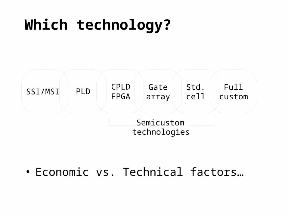
Which technology?
• Economic vs. Technical factors…
PLD Gatearray
Std.cell
Fullcustom
SSI/MSI
Semicustomtechnologies
CPLDFPGA

Evolution…
1960
1970
1980
1990
2000
SSI
MSI
LSI
VLSI
‘standard components’ ‘semicustom
components’
Gate Array
Standard cellsSimple PLD
CPLD FPGA

Economic factors…
.overhead..
cost Testing
costUnit Volume
cost NREcost Component
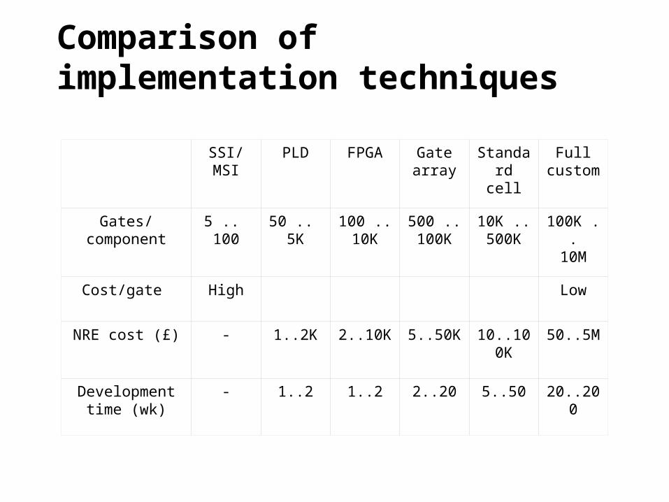
Comparison of implementation techniques
SSI/MSI PLD FPGA Gate array
Standard cell
Full custom
Gates/component
5 .. 100
50 .. 5K
100 ..10K
500 ..100K
10K ..500K
100K ..10M
Cost/gate High Low
NRE cost (£) - 1..2K 2..10K 5..50K 10..100K 50..5M
Development time (wk)
- 1..2 1..2 2..20 5..50 20..200

Comparison (2)
Circuit cost as a function of volume
Discrete
Full custom
Volume
Cost

Semicustom devices
• Mask-programmed devices are ‘customised’ by manufacturer
• Gate Array - Gates already fabricatedInterconnecting metalisationused to customise design
• Standard cell - similar to PCB layout, but using predefined cellsMore efficient, but requires fullmask set

Gate Array and Standard Cell layout
I/O pad
Logic gateRouting channel
A B
Vdd
Gnd
OUT
1 2
3 4

Cell layout may be optimised…
• As an example, consider a simple D-latch (1) constructed from gates only, and (2) by being able to exploit individual transistor characteristics
D
Enable
Q
Q
18 transistors
Transparent latch (1)
D
Enable
Q
Q
weak inverter
6 transistors
Transparent latch (2)

Programmable devices
• PROM - fixed AND array (decoder)programmable OR array (ROM
content)
• PLA - both arrays programmable allows p-term sharing
• PAL - fixed OR array(so faster, cheaper than PLA…)

Simple PLDs
• Basic AND-OR structure with high fan-in(8-12 variables per p-term)
• Output macrocells allow multiple output configurations within single package

PAL – most common PLD structure
• How beneficial is product sharing?– Not enough to justify the extra AND array
• PALs have fixed OR array– Each AND gate is permanently connected to a
certain OR gate.
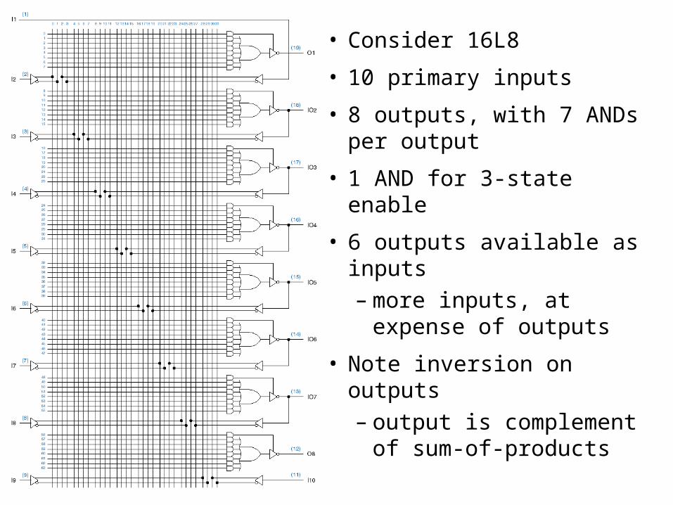
• Consider 16L8
• 10 primary inputs
• 8 outputs, with 7 ANDs per output
• 1 AND for 3-state enable
• 6 outputs available as inputs– more inputs, at expense
of outputs
• Note inversion on outputs – output is complement of
sum-of-products

GAL 16V8
• Finally got it right
• Each output is programmable as combinational or registered
• Also has programmable output polarity

GAL 16V8 output logic macrocell

22V10
• More inputs
• More product terms
• More flexibility

CPLDs vs FPGAs
• CPLD architecture
• Programmable interconnect between PLDs

• FPGAarchitecture
• Much larger number of smaller programmable logic blocks
• Embedded in a sea of of programmable interconnect

Trends in programmable devices…
• Current devices contain more than a million gates
• What can we do with them all?
• Increasing market in IP to provide standard functions
• Manufacturers including dedicated blocks (memory, CPU) plus programmable logic for ‘system-on-chip’ designs

IP functions
• MSI building blocks
• Maths functions
• Memories
• Processors
• Peripherals
• Bus Interfaces
• Communications
• Networking
• EDC/ECC functions
• Signal processing
• DSP
• May consist of ‘just’ source code or layout too…

‘SOC’ programmable devices
Excalibur Embedded Processor Solutions
Combining logic, memory, and a processor core, Altera's new Excalibur™ embedded processor solutions allow engineers to integrate an entire system on a single programmable logic device (PLD). The three families—the Nios™ soft core embedded processor, the ARM®-based hard core embedded processor, and the MIPS-based® hard core embedded processor—give you the flexibility of processor cores with the integration of system-on-a-programmable-chip (SOPC) logic.
Excalibur embedded processors can be used in a wide range of applications, from industrial instrumentation to DSL access concentrators. They offer full integration with Altera's APEX™ PLD architecture, and are supported by the Quartus™ development tool, which is optimized for the Excalibur embedded processor families.
Click the images below to learn more about Altera's Excalibur embedded processor solutions.
Last updated: Oct. 23, 2000 Technical support: [email protected] Comments: [email protected] Copyright © 1995 - 2000 Altera Corporation, 101 Innovation Drive, San J ose, California 95134, USA. All rights reserved. By accessing any information on this web site, you agree to be bound by the terms of Altera's Legal Notice.