computational study of confined states in quantum dots by
TRANSCRIPT

Computational Study of Confined States in Quantum Dots by an Efficient
Finite Difference Method
A THESIS
SUBMITTED TO THE FACULTY OF THE GRADUATE SCHOOL
OF THE UNIVERSITY OF MINNESOTA
BY
Salman Butt
IN PARTIAL FULFILLMENT OF THE REQUIREMENTS
FOR THE DEGREE OF
MASTER OF SCIENCE
Dr. Jing Bai
January 2010

© Salman Butt 2010

i
Acknowledgements Page
Acknowledgements
First of all, I’d like to thank my adviser Dr. Jing Bai to give me an opportunity to
work on this thesis project and to guide me throughout the course of this research. I’d
also like to thank Professor Mohammed Hasan and Professor Jonathan Maps to be
my committee members. Also, I’d like to thank Professor Imran Hayee for the TA
support and advice to help me achieve my goals towards my degree. Next, I’d like to
thank Professor Jiann-Shiou Yang for his support and advice as a professor and the
department head, Professor Scott Norr for his understanding and support during my
final semester as GTA and GRA, Professor Stanley Burns for his support, Professor
Tom Ferguson for his advice and support as well as the rest of the ECE faculty. In
addition, I’d like to thank our ECE office staff, Shey Peterson and Kathy Bergh for
their great support and always being available to answer questions. I’d like to thank
Marvin for his technical support in setting up our workstation and providing the
software(s) needed for our research. Specially, I’d like to thank the financial support
from Grant-in-Aid research award (PI: Dr. Jing Bai) from the graduate school of UM
and Dr. Jing Bai’s start-up fund from UMD. Not to forget, thanks to my colleagues
for their friendship and support. Finally, I’d like to thank my family very much
whose everlasting support gave me great motivation towards completion of my thesis
and my degree.

ii
Dedication
This thesis is dedicated to the UMD ECE dept.

iii
Abstract
Semiconductor quantum dot systems have gained more attention in quantum computation
and optoelectronic applications due to the ease of bandstructure tailoring and three-
dimensional quantum confinement. Thus, an accurate solution of energy bandstructure
within the quantum dot is important for device design and performance evaluation. In this
paper, the solutions of bandstructures of quantum dot systems are presented by
implementing finite difference technique. To illustrate our analysis procedure, various
configurations of quantum dot systems were taken into account. In order to improve the
calculation efficiency of the finite difference solution in terms of time and memory
consumption, uneven divisions for the quantum dot confinement region were used. In
addition, we identified the optimum combination of divisions for each geometrical
configuration. Eventually, the eigenstate wavefunctions and eigenvalues were obtained
by directly solving the eigen-value problems. Overall, the generated results agreed
consistently with the published results obtained by other solution techniques.
Keywords: quantum dots, confinement states, finite difference method

iv
TABLE OF CONTENTS
List of Tables...………….…………………….………………………………..….……vi
List of Figures …………….…………………….………………………………..….…vii
Chapter 1: Introduction ….…………………….………………………………..….……1
1.1. Background ………..…………………………………………………1
1.2. Objective ………………….………………………………………… 2
1.3. Scope ……………….……………………………………………….. 3
Chapter 2: Literature Review…......…………………………………………..………… 5
2.1. Structure and Applications of Quantum Dots …...…………….……..5
2.2. Structure and Applications of Quantum Dot Superlattice System…...9
2.3. Modeling strategies of QDs and QD-SL ……………………..…..... 13
2.3.1. Modeling strategy for individual & coupled QDs …..….……...13
2.3.2. Modeling strategy for QD-SL …………………..………..…… 13
Chapter 3: Theoretical Background ………………….……………..………..…….......15
3.1. Schrödinger equation for quantum system….………………….…...15
3.2. Finite Difference method ………………..….……………………... 16
Chapter 4: Finite Difference Solution for Quantum Well Systems …………….……...18
4.1. Solution Procedure ……………………………………..………...…18
4.2. Results and Discussions ……………………………..………......… 19
Chapter 5: Finite Difference Solution Procedure for Quantum Dot System ……….… 23
5.1. Finite Difference formulation for quantum dot system……………..23
5.2. Quantum Dots in cubic shape ………………………..……………..28
5.2.1. Physical configuration and finite difference mesh …………….28

v
5.2.2. Skills Used …………………………..………………….…….. 29
5.2.3. Convergent Eigen values & Optimum Combination Processes..29
5.2.4. Results …………………………………………...………….....29
5.3. Quantum Dots in cuboid shape ………….….………..……………. 32
5.3.1. Physical configuration and finite difference mesh …………….32
5.3.2. Skills Used …………………………..………………….……...33
5.3.3. Convergent Eigen values & Optimum Combination Processes..33
5.3.4. Results ………………….…………………….......…………....33
5.4. Quantum Dots in pyramid shape …….…….………..……………...35
5.4.1. Physical configuration and finite difference mesh …………….35
5.4.2. Skills Used …………………………..………………….…….. 39
5.4.3. Convergent Eigen values & Optimum Combination Processes..40
5.4.4. Results ………………….……………………...……………....42
5.5. Discussion on CPU Usage: Strategies for Limited Memory……….49
Chapter 6: Quantum Dot Superlattice …...……………………………….…………... 50
6.1. Solution Procedure …………………….………………….………. 50
6.2. Results ….…………………………………………………………. 51
Chapter 7: Conclusions & Future Recommendations …………..….…………...….… 55

vi
LIST OF TABLES
Table 1: Analytical Comparison for Double Pyramidal QD Results …………………. 46

vii
LIST OF FIGURES
Figure 2.1. Schematic bandstructure of a quantum dot ……………….…….…….…….6
Figure 2.2. Electronic state transition in QD lasers ……………….…….…….………...7
Figure 2.3. Semiconductor Fluorescence …..…………..…………….…….…….…….. 7
Figure 2.4. Undoped QD-SL grown on substrate ……..………..….....…….…….……..9
Figure 2.5. Cross-section of undoped QD-SL grown on substrate ……....….….…...….10
Figure 4.2. 1st 3 Eigen States for Single QW with 100 meV………….…….………..... 19
Figure 4.3. 1st 3 Eigen States for Double QW with 100 meV.………….………………20
Figure 4.4. 1st 3 Eigen States for Double QW with 520 meV….……….….………...... 21
Figure 4.5. 1st 6 Eigen Functions for Double QW with asymmetric barrier …...………22
Figure 5.6. 3D Mesh for Single Cubic QD ………………………..………….………..28
Figure 5.7. 1st Eigen State Wavefunction for Double Cubic QDs ..…..………………..30
Figure 5.9. 3D Mesh for Single Cuboid QD ..……………………..………….………..32
Figure 5.10. 1st Eigen State Wavefunction for Double Cuboid QDs ..……………….....34
Figure 5.11. 3D Model for Pyramidal QD in cuboid matrix…...…………………......... 35
Figure 5.12. Mesh for Single Pyramidal QD and Barrier cross-section………..….........36
Figure 5.13. Enlarged View of Mesh for transition region Single Pyramidal QD….......37
Figure 5.14. Mesh for Double Pyramidal QDs and Barrier cross-section ………….......38
Figure 5.15. Convergent Test Results for Double QDs ………………………..….........41
Figure 5.16. 1st Eigen State Wavefunction (xz) Double Pyramidal QDs ……………… 43
Figure 5.17. 1st Eigen State Wavefunctions (xy) Double Pyramidal QDs …………..… 44
Figure 5.18. Graphical Comparison for Single & Double Pyramidal QD Results …......47
Figure 5.19. Graphical Comparison for Double Pyramidal QDs Results ………..……..48
viii
Figure 6.6. QD-SL: Electron miniband vs Cubic QDs (Interdot distance fixed)..……...52
Figure 6.7. QD-SL: Electron miniband vs Interdot distance (QD size fixed) .……..…. 53
Figure 6.8. QD-SL: Density of States vs Energy levels ………….…..……..………… 54

1
Chapter 1. Introduction
1.1 Background
Quantum dots (QDs) are commonly known as “artificial atoms”, since they provide the
opportunity to control the energy states of carriers by adjusting the confinements in all
three spatial dimensions. The QD superlattice (QD-SL) structure consists of multiple
arrays of QDs as more information is provided below. Quantum dot structures have
extensive applications in quantum computations and optoelectronic applications/devices
[1]. The QD-SL structure has been attractive in making the intermediate-band solar cells
(IBSCs) [2-4]. The maturity of crystal growth technologies, such as molecular beam
epitaxy (MBE) and metal-organic chemical vapor deposition (MOCVD), has facilitated
the growth of quantum dots with various geometries for a wide selection of material
systems.
In order to further explore the potential of QD structure and increase performance of QD
devices, understanding of confined energy states in QD structures is necessary. Thus,
accurate and efficient solutions for confined states in single-QD and double-QD systems
are pivotal in providing constructive details to facilitate the understanding of the more
complex structure of QD arrays. In this study, both the confinement of individual QD
structures and the miniband structure formed by QD-SL are investigated. The
confinement states for an individual QD and two coupled QDs are investigated through
the finite difference solution approach for the time-independent Schrödinger Equation.
The solution is generalized from the solution of one-dimensional confinement of
quantum well (QW) structures, which has been well reported in the literature [5-7].

2
Moreover, the miniband confinement of QD-SL structure is solved from Envelope
Function Approximation method.
1.2 Objective
The objective of this research is to solve for confined Eigen state energies as a result of
computations and simulations within QD structures to develop further know-how for the
more practical QD-SL systems. Among all the theoretical and numerical solutions of the
1D and 3D Schrödinger’s equations, the finite difference method (FDM) provides an
efficient and a convenient way in treating QDs with various complex geometries, which
can best approximate the practical shapes of QDs (pyramid or diamond) from fabrication.
In principle, the FDM ends up with the solution of Eigen-value problems. Here, the
eigen-values correspond to the Eigen energy levels of the confined states and the Eigen-
vectors correspond to the eigen state wavefunctions. Due to the spanning in 3D, large
memory usage in the computation brings challenge when deriving the solution of FDM
for QD systems. In our current work, we develop a mesh strategy for efficient memory
usage in solving QD system by using the 3D finite difference methodology. In principle,
besides directly solving the Eigen-value problems, we reduce the memory usage through
division optimization in 3D along with application of dissimilar and uneven divisions
between the dot and barrier matrix regions. Our simulator results agree well with results
presented in other sources. In summary, the technique presented here is applicable to
structures with limited number of QDs. For systems which constitute a larger number of
packed QDs i.e. the QD-SL structure, different solution procedures such as the 3D
Kronig-Penney model and the Envelope Function Approximation methods are applied.
3
1.3 Scope
The scope of this thesis is to present solutions based on results from implementation of an
efficient meshing strategy in 3D FDM solution for configurations comprising of
vertically and horizontally aligned coupled QDs. Following the first chapter of our paper
i.e., the introduction, the rest of the thesis is arranged as follows. In Chapter 2, we discuss
the literature which includes the review on the QD and QD-SL structures and their
practical applications. In addition, existing modeling strategies in the literature for the
similar QD systems are reviewed. Such information based on analysis of results derived
from other resources has proven to be useful in laying a basis for our current work. In
Chapter 3, we present the basic theories i.e. the theoretical formulations for the QW and
QD structures. The Finite Difference Method solution procedure for time-independent
Schrodinger equations is outlined. In Chapter 4, we present the QW structure by outlining
the solution procedures and the results derived from simulations for QW systems with
single and multiple barriers. Even though the solution of 1-D QW structure by FDM has
been very well studied in the literature, we take this as the starting-point of our model and
then expand it to 3D for QDs. In Chapter 5, we explain the solution procedures and the
generated results for various QD configurations of vertical and horizontal alignment of
QDs with cubic, cuboid and pyramidal geometries. Details for the CPU usage are also
discussed along with highlighting the various strategies implemented to utilize less space.
In Chapter 6, we focus on the solution of the QD-SL structure derived from the Envelope
Function Approximation method.

4
In Chapter 7, we conclude our thesis by summarizing the results obtained from the work
along with future recommendations to further expand the scope of our work.

5
Chapter 2. Literature Review
In this chapter, we introduce the structures for quantum dots and quantum dot
superlattice, as well as their applications in optics and electronics. Also, we survey the
current existing modeling strategy for the quantum dot systems.
2.1 Structure and Applications of Quantum Dots
The term "Quantum Dot" was coined by Mark Reed [8]. They were discovered by Louis
E. Brus [8]. Typically, quantum dots are small regions defined in a semiconductor
material with electrons confined to all three spatial dimensions and a size of order
10~100 nm [9]. Resultantly, the properties embedded within them are between the ones
for bulk semiconductors and discrete molecules [10-13]. Since the first studies in the late
1980’s, the physics of quantum dots has been a very active and fruitful research topic
[14].
The name “dot” suggests an exceedingly small region of space [14]. A semiconductor
quantum dot, however, is comprised of roughly a million atoms with an equivalent
number of electrons. Virtually all electrons are tightly bound to the nuclei of the material,
however, the number of free electrons in the dot can be very small; between one and a
few hundred. The deBroglie wavelength [15], or matter wavelength of these electrons is
comparable to the size of the dot and the electrons occupy discrete quantum levels (akin
to atomic orbitals in atoms) and have a discrete excitation spectrum. A quantum dot has
another characteristic, usually called the charging energy, which is analogous to the
ionization energy of an atom. This is the energy required to add or remove a single
electron from the dot [14]. The quantum confinement states [16] are states consisting of
6
energy confined to three dimensions inside a dot as the dot is within range of less than
100 nm scale, hence minimized to a unit of physical entity i.e. quantum.
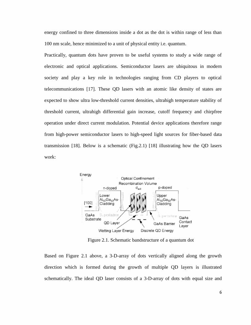
Practically, quantum dots have proven to be useful systems to study a wide range of
electronic and optical applications. Semiconductor lasers are ubiquitous in modern
society and play a key role in technologies ranging from CD players to optical
telecommunications [17]. These QD lasers with an atomic like density of states are
expected to show ultra low-threshold current densities, ultrahigh temperature stability of
threshold current, ultrahigh differential gain increase, cutoff frequency and chirpfree
operation under direct current modulation. Potential device applications therefore range
from high-power semiconductor lasers to high-speed light sources for fiber-based data
transmission [18]. Below is a schematic (Fig.2.1) [18] illustrating how the QD lasers
work:
Based on Figure 2.1 above, a 3-D-array of dots vertically aligned along the growth
direction which is formed during the growth of multiple QD layers is illustrated
schematically. The ideal QD laser consists of a 3-D-array of dots with equal size and
Figure 2.1. Schematic bandstructure of a quantum dot
(laser

7
shape surrounded by a higher bandgap material which confines the injected carriers [18].
Figure 2.2 below further illustrates the electronic state transition among the QD confined
energy levels in QD lasers.
Also, semiconductor fluorescent quantum dots are nanometer-sized functionalized
particles that display unique physical properties making them particularly well suited for
visualizing and tracking molecular processes in cells using standard fluorescence
microscopy [19-21]. Below is Figure 2.3 explaining how the semiconductor fluorescence
works [22]:
Figure 2.3. Semiconductor Fluorescence
Figure 2.2. Electronic state transition in QD lasers
http://www.lce.hut.fi/publications/annual2001/a0451x.gif
.
http://www.fluorescence-foundation.org/lectures/chicago2009/lecture10.pdf.

8
In addition, semiconductor nanocrystal or quantum dot flourophores offer a more stable
and qualitative mode of fluorescence in situ hybridization for research and clinical
applications [23]. Although, semiconductor nanocrystals have been investigated for
several decades [23-25], compatibility of these minute crystals with interesting electro-
optical properties has only recently been demonstrated in biological experiments. Other
applications of quantum dots include nanomachines, neural networks, high-density
memory, LEDs and diode lasers. As far as nanomachines go, the electron transfer rates
are computed from the free energy change for a single electron transfer to or from a
quantum dot of size such that only charge quantization matters. For a small enough
dot,
the nanomachine device could operate at room temperature [26]. In neural networks, the
neural model system is that of a quantum dot molecule [27, 28] with five dots arranged as
the spots on a playing card [29]. Also, metal nano-dot (MND) films consist of a thin
oxide film that includes high density metal dots with nano-scale (quantum) [30]. In
addition, quantum-dot LEDs (QD-LEDs) are fabricated that contain only a single
monolayer of QDs, sandwiched between two thin films [31]. Lastly, InGaN QDs have
proven to be useful for localization of carriers in purple laser diodes [32].

9
2.2 Structure and Applications of Quantum Dot Superlattice system
QD superlattices are artificial crystals whose building block is a QD [33, 34]. In other
words, QD superlattices are multiple arrays or stacks of QDs [35] aligned vertically and
horizontally in all the three spatial dimensions. High quality QD-SLs are made of
InGaAs/GaAs where GaAs is used for barrier material. Other materials for QD-SL
include Ge/Si. Following are graphs (Figure 2.4 and Figure 2.5) [4] that illustrate the
structure of the QD-SL:
Figure 2.4. Image of an undoped InGaAs/GaAs (20 nm) QD SL grown
on GaAs substrate.

10
Basically, superlattices of nanometer- sized QDs can be generated either in solution as
the crystallization of a monodisperse colloid or at a solid or liquid interface as a thin,
ordered superlattice of dots [36]. Self-assembled and self-organized Ge/Si quantum dot
(QD) superlattices (SLs) have been grown by a solid-source MBE system with the
Stranski-Kranstanov (SK) growth mode [37]. Under the SK growth mode, the formation
of quantum dots is driven by the strain during epitaxy growth of InGaAs on a GaAs
substrate as the deposited layer exceeds a critical thickness [38]. In MBE, the growth
temperature is kept around 500oC with InGaAs or InAlAs used as the dot material while
GaAs and AlGaAs as the cladding (covering) layers [39]. Meanwhile, in the MOCVD, as
Figure 2.5. Cross-section image of an undoped InGaAs/GaAs (20 nm) QD
SL grown on {113}B GaAs substrate.
11
in other growth techniques that involve molecular species, surface reactions play an
important role [39]. Besides, various geometric structures for QDs have been
implemented within the QD-SL systems. Arrays of cubic and pyramidal QDs are
common for the typical QD-SL configuration. Such intricate configurations and
structures have recently been studied as their complexities have led to a wide array of
potential practical applications. Among them, high efficiency thin-layer solar cells are
very well-known. Solar cells have been the main focus recently for practical purposes of
energy conversion and as a means of providing renewable energy. Such novel
semiconductor structures have been studied and researched as they are also referred to as
the IBSC, a generic class of photovoltaic devices [2]. Basically, the way the QD-SL solar
cells work is that inside them, the QDs are modeled as a regularly spaced array of equally
sized dots in the respective matrix. Incorporating the effect of silicon’s anisotropic
effective mass is shown to reduce both the degeneracies of the isotropic solutions and the
energy separation between states [3]. These photovoltaic arrays have been in demand in
recent times due to interest in cost-effective solutions for renewable energy conversion.
In addition to the solar cells, collective electronic phenomena have been predicted for the
three-dimensional ordered superlattices of QDs [40]. Some of these collective electronic
phenomena include electrical transport and observation of macroscopic properties of QD-
SL solids. Also, far-infrared radiation can directly induce optical transitions between the
meV energy levels confined in the quantum dots. Known to be narrow band gap
semiconductor, QDs have been found to exhibit a well‐defined structure and have
near‐unity quantum yield with emission wavelength between 1.2 microns and 2 microns
determined by the particle size. Thus QDs, especially PbSe, have potential for application
12
as a monochromatic infrared light source [41]. To achieve a detectable signal requires dot
arrays with active sample areas on the order of 10 mm2 [42]. One of the requirements for
technological applications is a high spatial density of dots. Toward this end, several
groups have grown quantum-dot superlattices. For example, alternating growth of GaAs
and strained InAs yields layers of InAs dots embedded in GaAs. A fascinating feature of
such structures is that the dots in successive layers are spatially correlated [43-47]. Each
of the 6 citations mentioned here has a particular growth technology used. In the first one,
the growth of multilayer arrays of coherently strained quantum dots is investigated as a
simple model reproduces the observed vertical correlation between QDs in successive
layers. In the second case, the superlattices and thick QD layers grown on (100), (111),
and
(110) Si surfaces by MBE exhibit different growth
morphologies and defect
structures. The third citation mentions transmission electron microscopy for study of
microstructure of strained layers of InxGa1−xAs/GaAs grown by MBE. Based on the
fourth source, coherent InAs QDs separated by GaAs layers are shown to exhibit self-
organized growth along the vertical (i.e., growth) direction. Finally, the last citation
discusses multi-layer, vertically coupled, quantum dot structures investigated by using
layers composed of InAs QDs grown by MBE in the S-K growth mode. QD-SL structures
with distribution of density of states and discrete energy levels due to three-dimensional
quantum confinement provide the potential for better thermoelectric devices [48]. The
MBE growth of self-assembled QD-SL materials on planar substrates using the Stranski-
Krastanov growth mode yields improved thermoelectric (TE) figures of merit [49, 50].
Self-assembled quantum dot materials represent just one of a number of new approaches
[51] being investigated in order to enhance TE performance.
13
2.3 Modeling strategies of quantum dots and quantum dot superlattices
2.3.1 Modeling strategy for individual and coupled quantum dots
To develop a further practical understanding of the QD and the more complex QD-SL
structures, numerous modeling strategies and methodologies have been implemented to
solve for various significant factors including the confined eigenstate values. Such values
are integral as they are associated with energy values and eigenstate functions which help
in further understanding the properties imbedded within the material used for these
structures. For QD structures, finite difference method is used [52-54]. In order to save
memory in the solution procedure, the resulting eigen-value problem is transferred to the
solution a set of linear equations [52], provided that an appropriate perturbation value is
chosen. This perturbation has to be a non-zero value, otherwise the solution to this system
of linear equations would be uniformly zero. Another source implements the Jacobi-
Davidson [53] based method to solve for eigen-value problem after initially applying the
FDM [61]. Here, the Jacobi-Davidson method is used to compute the smallest possible
eigenvalues and the associated eigenvectors which involves the orthonormality and
orthogonality of the eigenvectors.
2.3.2 Modeling strategy for quantum dot superlattice
As far as the QD-SL systems go, similar modeling strategies are executed by
implementing the Envelope Function Approximation or Effective Mass Approach [3, 35].
This method involves assumption of electron potential to be a sum of three independent

14
periodic functions in orthogonal directions. Using this approach, the resulting potential is
separable into three independent components allowing carrier dispersion relation to be
obtained from the sum of solutions in each spatial direction. Here, multiple arrays of
cubic QDs are stacked together vertically and horizontally to form a QD-SL system
configuration. Models used are mathematically based upon the methods mentioned above
which are similar to the Kronig-Penney Model [55]. This model deals with single
electron moving in a one-dimensional crystal. It requires use of Bloch and hyperbolic
functions with product of the traveling wave solutions and a periodic function. That
function has the same periodicity as the potential. Overall, this model leads to both real
and imaginary solutions corresponding to the propagating and the forbidden electron
states. Also, as mentioned before, large memory consumption is the main problem for
computation of eigen values due to the spanning of the 3D structure. In our current work,
we present an efficient mesh strategy to save the memory in solving the eigen-value
problem resulting from 3D finite difference method. This method reduces the
computational memory in a different way compared to the method presented in
Harrison’s paper [52].

15
Chapter 3. Theoretical Background
3.1 Schrödinger equation for quantum system
The confinement states in a quantum system are analyzed through the Schrödinger
equation. The Schrödinger equation is as central to quantum mechanics as Newton's laws
are to classical mechanics. Solutions to Schrödinger's equation describe not only atomic
and subatomic systems, atoms and electrons, but also macroscopic systems [56].
The standard time-independent 1-D Schrödinger equation (3.1) [57-59] is as follows:
)()()(][2 2
22
xExxUdx
d
m
(3.1)
U corresponds to the quantum barrier potential, which is dependant on the spatial
dimensions, E represents the eigenenergy of the system energy, ψ symbolizes the
wavefunction of the corresponding eigenstate, ħ is the Planck’s constant and m is the
electron effective mass. The Schrödinger equation can be applied to solve the quantum
well system, where degree of electron freedom (Df) is 2 and degree of electron
confinement (Dc) is 1 as Df + Dc = 3 for all solid state systems [59].
For the electronic bandstructure of a quantum dot system, since the confinement is in 3D,
the confinement states can be described by the 3D time-independent Schrödinger’s
Equation (3.2) [58-60]:
),,(),,(),,(][2 2
2
2
2
2
22
zyxEzyxzyxUzyxm
(3.2)

16
Basically, different m was used for the QD and the matrix regions. For consistent
comparison with results derived from Harrison’s paper, same m was used for the QD and
matrix regions.
3.2 Finite Difference Method
The finite difference method approximates solutions to differential equations by replacing
derivative expressions with approximately equivalent difference quotients [63]. As far as
the derivation procedure for the finite difference method goes, the first derivative of is:
,)()(
lim)('0 x
xxxx
x
(3.3)
A reasonable approximation for that derivative would be:
,)()(
)('x
xxxx
(3.4)
for small value of Δx. This is known as the forward difference equation for the first
derivative. The approximation for the second-order derivative in FDM would be:
,)(
)()(2)()(''
2x
xxxxxx
(3.5)
which is important to solve the Schrödinger equation since the Schrödinger equation
involves the second-order derivative. The 1-D Schrödinger equation along the x-axis is as
follows, which can be used to solve for the 1-D quantum-well system:
)()()()(])(
)()(2)([
2 2
2
xxExxUx
xxxxx
m
(3.6)
17
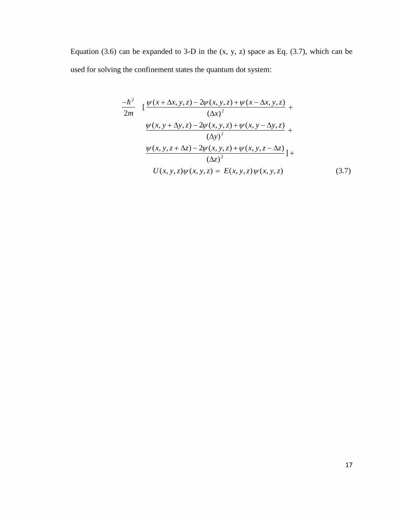
Equation (3.6) can be expanded to 3-D in the (x, y, z) space as Eq. (3.7), which can be
used for solving the confinement states the quantum dot system:
)7.3(),,(),,(),,(),,(
])(
),,(),,(2),,(
)(
),,(),,(2),,(
)(
),,(),,(2),,([
2
2
2
2
2
zyxzyxEzyxzyxU
z
zzyxzyxzzyx
y
zyyxzyxzyyx
x
zyxxzyxzyxx
m

18
Chapter 4. Finite Difference Solution for Quantum Well Systems
4.1 Solution Procedure
The primary purpose for implementation of finite difference method on QWs is to
understand the finite different solution which helps in expanding the formulation to 3D
for more complex systems. In other words, solving for QW system helps explain the
behavior patterns of the electron along with the basic knowledge of the eigen state energy
pattern in 1D system.
Mathematically, the 1-D Schrödinger’s equation for FDM (3.6) as above is used for the
quantum well system. Matrix A (the term in brackets which is multiplied by –h2/2m in
Eq. (3.6)) along with rest of parameters for Eq. (3.6) are below:
ijjij
N
QW ExxUxAas
x
x
x
xA
)()()(
)(
)(
)(
,
21
...
121
121
12
)(
1 2
1
2 (4.1)
The barrier material used is AlInAs and the quantum well material is InGaAs.
Simulations were performed for both single and double QW along with position varying
electron effective mass and constant electron effective mass. For the single QW system,
the dimensions along x-axis for both the left and right barrier lengths were 25 nm and the
quantum well 50 nm. For the Double QW system, the dimensions for the left and right
barriers were kept at 25 nm while the middle barrier at 20 nm. Both the quantum wells
were restricted to 15 nm each.

19
4.2 Results and Discussions
In Figure 4.2 below, it is observed that eigenenergies are increasing based on n2 i.e. E2 ≈
22 E1 and E3 ≈ 3
2 E1. Also, it can be seen how the barrier widths affect the change in the
wavefunctions especially at the boundaries. Besides, the shapes of the wavefunctions
correspond correctly to the relative confined energy i.e. the 1st energy wavefunction has
extremum, the 2nd
has two extrema and the 3rd
has three. The extrema correspond to the
highest electron probability density. These characteristics of the wavefunctions
appropriately reflect the behavior of the particle(s) inside the quantum well.
n = 1
E2=4.326 meV
E1=1.087 meV
E3=9.680 meV
x (nm)
0
0
10 20 30 40 50 60 70 80 90 100
5
10
Ψ2(x)
Ψ3(x) n = 3
n = 2
Ψ1(x)
Figure 4.2. Results from Matlab for 1st 3 Eigen States for Constant Electron Effective
Mass in Single QW with potential of 100 meV
Ener
gy (
meV
)

20
In Figure 4.3 below, the first three relative eigen energies along with their respective
wavefunctions are displayed. The barrier potential is same as above but the well region is
reduced to 2 wells of 15 nm each with additional barrier region of 20 nm in the middle
which increases the eigen energies below. Also, the wavefunctions with even n are the
degenerate states for the respective odd n i.e. n=1&2 correspond to the same eigenstate.
Figure 4.3. Results for 1st 3 Eigen State Wavefunctions for Constant Electron
Effective Mass in Double QW with finite potential of 100 meV
10 20 30 40 50 60 70 80 90 100 0
0
2
4
6
8
10
12
x (nm)
n = 1 Ψ1(x)
n = 3 Ψ3(x)
n = 5 Ψ5(x)
E5=11.0436 meV
E3=4.9409 meV
E1=1.2401 meV
100 meV 100 meV 100 meV 0 meV 0 meV
Ener
gy (
meV
)

21
In Figure 4.4 below, similar behavior is observed for the wavefunctions except this time
the barrier potential has been increased to 520 meV.
Figure 4.4. Results for 1st 3 Eigen State Wavefunctions for Varying Electron Effective
Mass in Double QW with potential of 520 meV
E1=0.02256 eV
E3=0.09080 eV
E5=0.20511 eV 0.2
0.1
0
0 10 20 30 40 50 60 70 80 90 100
x (nm)
n=1 Ψ1(x)
n=3 Ψ3(x)
n=5 Ψ5(x)
B
(520 meV)
B
(520 meV)
B
(520 meV)
W
(0 meV)
W
(0 meV)
Ener
gy (
eV)

22
In Figure 4.5 below, the difference in the corresponding or relative wavefunctions can be
noticed due of the asymmetry of the barrier widths. The top two eigenfunctions represent
11st
eigenstate, the next two as 2nd
eigenstate and the bottom two for 3rd
eigenstate.
10 20 30 40 50
x (nm)
60 70 80 90 100 0
10 20 30 40 50
60 70 80 90 100 0
10 20 30 40 50
60 70 80 90 100 0
10 20 30 40 50
60 70 80 90 100 0
10 20 30 40 50
60 70 80 90 100 0
10 20 30 40 50
60 70 80 90 100 0
0.5
0
-0.5
0.5
0
-0.5
0.5
0
-0.5
0.5
0
-0.5
0.5
0
-0.5
0.5
0
-0.5
Ψ(x)
Figure 4.5. 1st 6 Eigenfunctions for Varying Electron Effective Mass in Double QW

23
Chapter 5. Finite Difference Solution Procedure for Quantum Dot
System
In this chapter, we present the finite difference formulation for the 3D quantum dot
system using even division lengths for cubic and cuboid geometries meanwhile using
uneven division lengths for the pyramidal geometry.
5.1 Finite Difference formulation of the quantum dot system
Equation (3.2) above is solved through the finite different method, in which the quantum
box of dimensions Lx, Ly and Lz can be discretized along each coordinate axis, with nx
divisions along x axis, ny along y axis and nz along z axis. For even division lengths, Δx =
Lx/nx, Δy = Ly/ny and Δz = Lz/nz were used. For uneven division lengths, the following
equations were used:
x1 n1: ii xwherexxfromrangingx , (5.1a)
y1 n1: jj ywhereyyfromrangingy , (5.1b)
z1 n1: kk zwherezzfromrangingz , (5.1c)
The indexes are defined in terms of i, j and k along x, y and z axes with ranges 1 ≤ i ≤ nx,
1 ≤ j ≤ ny and 1 ≤ k ≤ nz. Therefore, k-1 and k+1 represent the corresponding neighboring
points along z-axis, j-1 and j+1 along y-axis and i-1 and i+1 along x-axis.
Next, Equation (3.2) is transformed as follows:

24
.
111111
2
2
,,
,,,,
1
2
1
2
1
2*
2
1
1,,
2
1,,
1
,1,
2
,1,
1
,,1
2
,,1
*
2
kji
kjikji
kkkjjjiiie
kk
kji
k
kji
jj
kji
j
kji
ii
kji
i
kji
e
E
Uzzzyyyxxxm
zzzyyyxxxm
(5.2)
Here, *
em is effective mass of electron.
Equation (5.2) is then distributed in matrix A as follows:
AQD =
nznynxnznynx
ijkrkji
ijkpi
bjkbkj
ajkaj
kk
,,
111111
11
1111
111
22121
1111
000000
000000000
0000000
00000
000000
0
00000
000000
(5.3)
Here, α is varying, diagonally across the matrix A as
[
1
2
1
2
1
2*
2 111111
2 kkkjjjiiie zzzyyyxxxm
] since uneven
division lengths were used whereas for a uniform 3D mesh is ])(
1[6
2h where ∆h =
(nx * ny * nz) rows and columns

25
∆x = ∆y = ∆z. The rest of the corresponding non-zero column elements are represented
by neighboring points with values varying due to uneven division lengths i.e.
1
2
11
kkkzz
andz
fromranging (5.4a)
1
2
11
jjjyy
andy
fromrangingY (5.4b)
1
2
11
iiixx
andx
fromrangingX (5.4c)
relative to the z, y and x coordinates respectively.
Based on matrix A above, every diagonal element represents a particular index location
point of a 3D system. The rest of the column elements for each diagonal value represent
the relative neighboring point positions. For instance, the diagonal element from the 1st
row represents index location for a corner point in 3D. Corner points are recognized as
points with i = j = k = 1, i = j = 1 and k = nz, i = k = 1 and j = ny, i = 1 with j = ny and k =
nz, j = k = 1 and i = nx, j = 1 with i = nx and k = nz, i = z = 1 and j = ny and finally i = nx
with j = ny and k = nz. Therefore, there would be a total of 8 corner index location points
in a 3D barrier box. An example of a corner point would be (1,1,1). The corresponding
2nd
column element would represent the neighboring point relative to k+1 i.e. (1,1,2). The
(nz + 1)th
column element represents the neighboring point relative to j+1 i.e. (1,2,1).
Similarly, the (nz ny + 1)th
column element represents the neighboring point along x-axis
corresponding to i+1 i.e. (2,1,1). Hence, there would be 3 valid neighboring points for the
corner index location. In another case, the diagonal element of the (nz + 1)th
row would
be a representation of an index location point on the edge. Here, one of the edge points
26
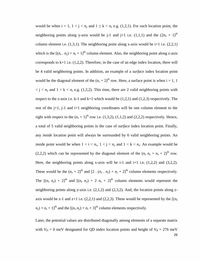
would be when i = 1, 1 < j < ny and 1 ≤ k < nz e.g. (1,2,1). For such location point, the
neighboring points along y-axis would be j-1 and j+1 i.e. (1,1,1) and the (2nz + 1)th
column element i.e. (1,3,1). The neighboring point along x-axis would be i+1 i.e. (2,2,1)
which is the [(nz . ny) + nz + 1]th
column element. Also, the neighboring point along z-axis
corresponds to k+1 i.e. (1,2,2). Therefore, in the case of an edge index location, there will
be 4 valid neighboring points. In addition, an example of a surface index location point
would be the diagonal element of the (nz + 2)th
row. Here, a surface point is when i = 1, 1
< j < ny and 1 < k < nz e.g. (1,2,2). This time, there are 2 valid neighboring points with
respect to the z-axis i.e. k-1 and k+1 which would be (1,2,1) and (1,2,3) respectively. The
rest of the j+1, j-1 and i+1 neighboring coordinates will be one column element to the
right with respect to the (nz + 1)th
row i.e. (1,3,2), (1,1,2) and (2,2,2) respectively. Hence,
a total of 5 valid neighboring points in the case of surface index location point. Finally,
any inside location point will always be surrounded by 6 valid neighboring points. An
inside point would be when 1 < i < nx, 1 < j < ny and 1 < k < nz. An example would be
(2,2,2) which can be represented by the diagonal element of the (nz ny + nz + 2)th
row.
Here, the neighboring points along x-axis will be i-1 and i+1 i.e. (1,2,2) and (3,2,2).
These would be the (nz + 2)th
and [2 . (nz . ny) + nz + 2]th
column elements respectively.
The [(nz ny) + 2]th
and [(nz ny) + 2 nz + 2]th
column elements would represent the
neighboring points along y-axis i.e. (2,1,2) and (2,3,2). And, the location points along z-
axis would be z-1 and z+1 i.e. (2,2,1) and (2,2,3). These would be represented by the [(nz
ny) + nz + 1]th
and the [(nz ny) + nz + 3]th
column elements respectively.
Later, the potential values are distributed diagonally among elements of a separate matrix
with VD = 0 meV designated for QD index location points and height of VB = 276 meV

27
(used in the case of pyramidal QD) for Barrier index points. This matrix is significant as
it shows what potential is used for a particular barrier. Importantly, because of the QD
geometry, all the middle diagonal values are not VD but actually distributed based on the
barrier and quantum dot location or index points. To explain more clearly, all the index
location points starting from (1,1,1) till the index point before QD region were distributed
diagonally with value of VB. All the points after the last index location point of the QD
region till the last index location point of the Barrier box i.e. (nx , ny , nz) were also
diagonally assigned the value of VB. For the matrix elements representing the middle
region including both the QD and MBL (Middle Barrier Length) regions, all the diagonal
elements of the potential matrix were initially set to VB. Then, those middle diagonal
elements were systematically chosen by matching with the QD region index location
points and accordingly assigned with value of VD. The general potential matrix is as
follows:
B
B
BD
B
B
V
V
VorV
V
V
V
00
000
000
000
000
(5.5)

28
5.2 Quantum Dots in cubic shape
5.2.1 Physical configuration and finite difference mesh
For cubic quantum dot, the material for the dot region was selected as InGaAs. Because
of even symmetry in shape, the dimensions used for the dot were similar for all the three
coordinates. The 3D mesh structure as follows was generated to clearly explain and
illustrate the geometry for the cubic QD. The mesh shown below is not up to scale based
on the calculations below as a cross-section of the actual diagram is presented to show
the mesh lattice structure and the geographical placement of the cubic QD. Information
regarding the division lengths, memory and the calculation time are presented later.
Figure 5.6. 3D Mesh for a Single Cubic QD
35 35
25
15
30
20
10
5
35
30
25
20
15
10
5
0
z
25 15
30 20
10 5
x
y

29
5.2.2 Skills Used:
Even division lengths were used between dot and barrier region.
5.2.3 Convergent Eigen values and Optimum Combination Processes
Please see section 5.4.3 below.
5.2.4 Results
Following are results generated from simulations for coupled or double cubic QDs
aligned along x-axis. Due to similar and consistent geometrical shape along all three
axes, the results are similar mathematically for Double cubic QDs aligned along z-axis as
well. The parameters used for this computation were: divisions combination of 36x36x36
for nx ny nz, barrier box dimensions of 24x24x24 nm3, cubic QDs dimensions as 6x6x6
nm3, barrier potential of 520 meV, dot material as InGaAs i.e. effective mass constant of
0.043. Division lengths for the dot region were ≈ 0.35 nm/div and ≈ 0.7 nm/div for the
barrier region. Memory utilization was less than 11 MB and calculation time less than 1
hour.
30
Resultantly, the Code Output Eigenstate Results are as follows:
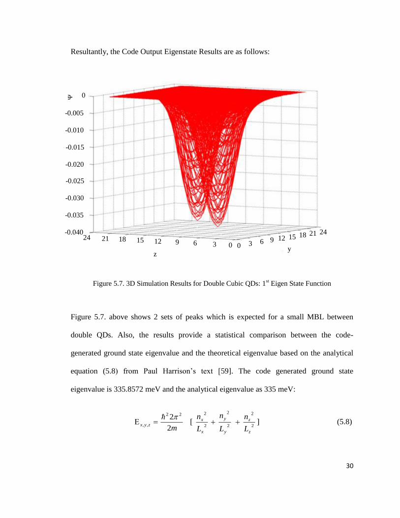
Figure 5.7. 3D Simulation Results for Double Cubic QDs: 1st Eigen State Function
Figure 5.7. above shows 2 sets of peaks which is expected for a small MBL between
double QDs. Also, the results provide a statistical comparison between the code-
generated ground state eigenvalue and the theoretical eigenvalue based on the analytical
equation (5.8) from Paul Harrison’s text [59]. The code generated ground state
eigenvalue is 335.8572 meV and the analytical eigenvalue as 335 meV:
][2
22
2
2
2
2
222
,,
z
z
y
y
x
x
zyxL
n
L
n
L
n
m
(5.8)
0
-0.005
-0.010
-0.015
-0.020
-0.025
-0.030
-0.035
-0.040
0 0 3 6 9 12 15 18 21 24
3 6 9 12 15 18 21 24
y z
Ψ

31
Based on the results above, a 0.25% discrepancy statistically verifies the accuracy and
authenticity of the results derived from our programming code for QDs with cubic
configuration. Overall, we can see how the confinement energies change between the
QW and QD as such additional effect of the 3D confinement makes an influence since
the number of eigen energies changes hence affecting the eigen states as well.

32
5.3 Quantum dots in cuboid shape
5.3.1 Physical configuration and finite difference mesh
For the cuboid quantum dot, the material for the dot region was also selected as InGaAs.
The 3D mesh structure as follows was generated to clearly explain and illustrate the
geometry for the cuboid QD. The mesh shown below is not up to scale based on the
calculations below as a cross-section of the actual diagram is presented to show the mesh
lattice structure and the geographical placement of the cuboid QD. Information regarding
the division lengths, memory and the calculation time are presented later.
Figure 5.9. 3D Mesh for Single Cuboid QD
25
20
15
0
0
5 10
15 20
30 25
35
x
5
10
15
20
30
25
35
y
z

33
5.3.2 Skills Used:
Even division lengths were used between dot and barrier region.
5.3.3 Convergent Eigen values and Optimum Combination Processes
Please see section 5.4.3 below.
5.3.4. Results
Following are results generated from simulations for coupled or double cuboid QDs
aligned along z-axis. Figure 5.10 show the eigen state wavefunctions generated. The
parameters used for this computation were: divisions combination of 36x36x36 for nx ny
nz, barrier box dimensions of 30x30x30 nm3, cuboid QDs dimensions as 12x12x6 nm
3,
barrier potential of 520 meV, dot material as InGaAs i.e. effective mass constant of
0.043. Division lengths for the dot region along x and y axis were ≈ 0.35 nm/div and ≈
0.2 nm/div along z axis. Division lengths for the barrier region were ≈ 0.8 nm/div.
Memory utilization was less than 11 MB and calculation time less than 1 hour.

34
Figure 5.10. 3D Simulation Results for Double Cuboid QDs: 1st Eigen State Function
z x
0
-0.01
-0.02
-0.03
-0.04
-0.05
-0.06
0 4
8 12
16 20
24 28
0 4
8 12
16 20
24 28
Ψ
35
5.4 Quantum dots in pyramid shape
5.4.1 Physical configuration and finite difference mesh
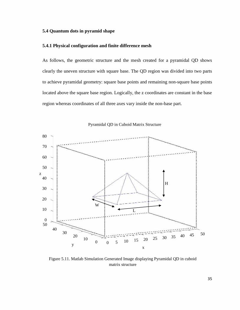
As follows, the geometric structure and the mesh created for a pyramidal QD shows
clearly the uneven structure with square base. The QD region was divided into two parts
to achieve pyramidal geometry: square base points and remaining non-square base points
located above the square base region. Logically, the z coordinates are constant in the base
region whereas coordinates of all three axes vary inside the non-base part.
Figure 5.11. Matlab Simulation Generated Image displaying Pyramidal QD in cuboid
matrix structure
80
70
60
50
40
30
20
10
0
z
40 30
20 10
0
50
50
0 y x
5 10 20 15 25 30 35 40 45 50
Pyramidal QD in Cuboid Matrix Structure
L
H
W
36
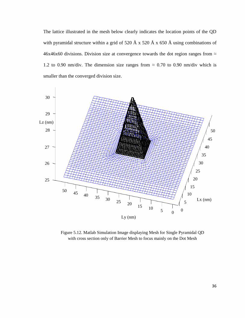
The lattice illustrated in the mesh below clearly indicates the location points of the QD
with pyramidal structure within a grid of 520 Å x 520 Å x 650 Å using combinations of
46x46x60 divisions. Division size at convergence towards the dot region ranges from ≈
1.2 to 0.90 nm/div. The dimension size ranges from ≈ 0.70 to 0.90 nm/div which is
smaller than the converged division size.
Figure 5.12. Matlab Simulation Image displaying Mesh for Single Pyramidal QD
with cross section only of Barrier Mesh to focus mainly on the Dot Mesh
25
26
27
28
29
30
Lz (nm)
25 35
45
15
50 40
30 20
10 5 0
Ly (nm)
Lx (nm)
0
5
10
15
25
35
45
50
40
30
20

37
Due to symmetrical configuration, the concept for geometry of double cubic QDs was
similar to single cubic QD. In the case of double pyramidal QDs, it was very similar as
well to the single pyramidal QD which is also mentioned above. For specification
purposes, the widths used for Barrier Box were 52nm x 52nm x 65 nm or 520 Å x 520 Å
x 650 Å (x,y,z) whereas QD1 and QD2 pyramid dimensions were 14nm x 14nm base
with height 7nm and 12nm x 12nm base with height 6nm respectively. Division size at
convergence for larger dot ranges from ≈ 1.2 to 0.90 nm/div whereas for the smaller dot it
ranges from ≈ 1.1 to 0.80 nm/div. The dimension size for larger dot ranges from ≈ 0.70 to
0.90 nm/div whereas for the smaller dot ≈ 0.60 to 0.80 nm/div which is smaller than the
converged division size. Figure 5.14 as follows illustrates the geometry for Double QD
pyramids (14nm and 12nm) aligned vertically along the z-axis with MBL = 70 Å:
Figure 5.13. Enlarged view at the region between the dot and matrix region to show
the element size transition

38
Figure 5.14. Matlab Simulation Image displaying Mesh for Double Pyramidal QDs again
with cross section only of Barrier Mesh to focus mainly on the Dot Mesh
34
33
32
31
30
29
28
27
26
25
Lz (nm)
Ly (nm)
40 45 50
Lx (nm)
40
45
50
30
35
25
10
15
20

39
5.4.2 Skills Used
Uneven division lengths were used for the Barrier Box and the QD regions. The reasons
for applying uneven division lengths were primarily for achieving better accuracy in
computation using lesser divisions and for smoother transition of confined Eigen States
while satisfying boundary conditions. This was implemented by using approximately
twice the number and uneven divisions for quantum dot regions compared to that of the
barrier region. For instance, in the case of total of 46 x 46 x 60 divisions, there were
uneven division lengths for ∆x, ∆y and ∆z for the QD and barrier regions. For QD, LxD =
14 nm for the larger QD and LxD = 12 nm for the smaller QD were used. Hence, ∆x for
QD was kept within range of 0.70 nm/division and 0.90 nm/division whereas for the
barrier box, ∆x was close to 1.2-1.5 nm/division. Similarly for y-axis, LyD = 14 nm for the
larger QD and LxD = 12 nm for the smaller QD were used. Hence, ∆y for QD was kept
within similar range compared to ∆x. Also, uneven division lengths were applied for the
transition regions between the barrier and the QD regions. In the case of vertically
aligned QDs, the division lengths along the z-axis were not even also as uneven divisions
were distributed for the QDs while dealing with the MBL division lengths as well.
Overall, uneven division lengths were used along the three axes for the barrier regions
and the QD regions for attaining convergence and accuracy in Eigen state results while
using lesser divisions. Based on the uneven division sizes mentioned above, mesh
division sizes in Harrison’s paper were consistent and even ranging close to ≈ 0.98
nm/div. Also 53x53x53 elements were used according to his paper instead of our
46x46x60 elements. Our mesh is more efficient since it gives us flexibility and utilizes
smaller memory by using lesser divisions because of uneven division lengths.

40
5.4.3 Convergent Eigen values and Optimum Combination Processes
In general, by utilizing the latest MATLAB [62] software available (Version: 7.7.0. 471 –
R2008b), the process is initiated by executing code simulations using various
combinations of divisions. Numerous computations were necessary to accomplish
convergent Eigen values based on determining the optimum combination of divisions.
These combinations are a product of the number of divisions i.e. nx ny nz in all the three
spatial coordinates. Based on our CPU memory allocation, the product of these divisions
was kept less than or equal to the threshold number of 563 or 175616. This threshold
number was determined based on the capability of our machine with limited memory to
compute and generate Eigen state results without utilizing elongated time periods for
simulations. Also, various combinations were used systematically for each simulation to
achieve convergent results. For Double QDs aligned along z-axis, an assortment of
combinations was embedded and tested within our codes for each varying MBL (1-9 nm
or 10-90 Å). Such strategy is illustrated as follows (Figure 3) which shows Convergence
Tests for Double QDs with MBL = 1 nm. Combinations in nx ny nz format include
49x47x73, 49x48x73, 49x49x72 and 50x48x72 which correspond to 168119, 171696,
172872 and 172800 divisions respectively. These combinations were derived based on
the fact that the less significant nx and ny division values were chosen to be equivalently
low and while a greater value selected for the more pertinent nz. The overall product was
kept within the range of the threshold value mentioned above i.e. 175616. Importantly,
the number of divisions represents the number of Eigen states as well. Overall, applying
these systematic strategies enhances the performance of simulations hence generating the
desired results with better accuracy and consistency. As a result, a smooth convergence

41
trend, comprising of the last 3 combinations of divisions, is observed and circled below in
Figure 5.15:
Figure 5.15. Convergent Test Results for Double QDs with MBL = 1 nm
Statistically, the convergence pattern observed above is highlighted due to the reasonably
minute ground state eigen value differences among the last 3 systematic combinations.
Based on further observation, the % diff and the ground state eigenvalue difference
between the last 2 combinations (denoted by ∆ in meV) are minimal. Therefore, the
optimum combination is represented by 50x48x72 based on the threshold of the machine.
Based on observation, the latest division combination reflecting convergence after
implementing uneven division lengths was recorded as 46x46x60.
Overall, computations involving very large numbers of divisions are necessary to achieve
more accurate results. In addition, based on recurrent observations, the simulation
process for each combination close to the threshold value of 175616 divisions takes up to
150
145
140
135
130
125
120
Gro
und S
tate
Eig
en V
alu
e (m
eV)
Systematic Combinations vs Ground State Eigen Values
49*47*73 49*48*73 49*49*72 50*48*72
convergence region
137.7454
140.2578 140.5044 140.5054

42
2.5-3 hours on average. Based on the latest divisions using uneven divisions, the
simulation process takes about 1.5 hours on average hence increasing overall efficiency.
5.4.4 Results
The mc and the potential barrier height (Vo) parameters used for cubic and pyramidal
QDs were: mc for Cubic QDs = 0.043, mc for Pyramidal QDs = 0.0665 (same as
Harrison’s paper for comparison), barrier potential for Cubic case = 520 meV and barrier
potential for Pyramidal case = 276 meV.
Following are results generated from simulations for pyramidal QDs aligned along z-
axis:

43
Figure 5.16. 1st Eigen State energy wavefunction (xz) for Double QD pyramids at y = 26 nm with
MBL = 5 nm

44
Figure 5.17. 1st Eigen State energy wavefunctions for Double QD pyramids with MBL = 10 nm
at z = 68, 29 and 1 nm respectively
0
0
15
10
5
0 60
50 40 30 20
0 0 10
60 50 40 30 20 10 x y
50 40 30 20 0 0 10
60 50 40 30 20 10
x y
60
50 40
30 20
0 0 10
60 50
40 30
20 10
x y
Ψ(x, y, z = 68nm)
Ψ(x, y, z = 29nm)
Ψ(x, y, z = 1nm)
6
4
2
0
x 105
2
1
0 60
x 1013
60
60

45
As we can see from the wavefunction above, there is a peak in the center of x-y plane as
the geometry for the pyramidal QDs is symmetric along x and y planes. This was also
noticed in the mesh plots before. Also, the trend can be noticed for the wavefunctions as
there is a variation with the z axis i.e. when z = 1, 29 and 68 nm. The wavefunction has
the largest magnitude among the three when z = 1 nm. At z = 29 nm, the magnitude of
wavefunction decreased and it occupies greater area for the grid. Such variation trends
help understand better about the QD confinement as the behavior of the particles and
eigen states within the dot with confinement in all the three planes. Also, the pyramid
double-dot confinement with the single-dot pyramid case in the previous section shows
the effect from the additional dot i.e. how having the middle barrier length affects the
behavior of the eigen states.
Next, for the case of convergent ground state eigenvalues for Single QD pyramid and
Double QD pyramids along the vertical axis, an in-depth mathematical analysis is shown
below (Table 1). Significantly, this analysis highlights the close comparison between our
code simulation results using direct eigensolver and the results based on a simpler
computation procedure for eigen values using linear equation solutions. Consistently, the
initial formulations applied in both cases involved implementation of FDM. The code-
generated convergent Eigen value results along with the published Eigen values in meV
are recorded as follows:
46
MBL Code EVs
Single
QD pyr
Published
EVs Single
QD pyr
EV diff (∆)
and %
Discrepancy
(D)
Code EVs
Double
QD pyrs
Published
EVs
Double
QD pyrs
EV diff (∆)
and %
Discrepancy
(D)
0 nm 147.2614 147.59 ∆≈0.3286
D≈0.2226%
N/A
N/A
N/A
1 nm
N/A
N/A
N/A 139.2957 139.70 ∆≈0.4043
D≈0.2894%
2 nm
N/A
N/A
N/A 143.8438 144.30 ∆≈0.4562
D≈0.3161%
3 nm
N/A
N/A
N/A 146.0079 [144.30-
147.10]
∆<1
D<1%
4 nm
N/A
N/A
N/A 146.7599 147.10 ∆≈0.3401
D≈0.2312%
5 nm
N/A
N/A
N/A 146.9541 [147.10-
147.59]
∆<1
D<1%
7 nm
N/A
N/A
N/A 147.1112 [147.10-
147.59]
∆<1
D<1%
9 nm
N/A
N/A
N/A 147.1980 [147.10-
147.59]
∆<1
D<1%
10 nm
N/A
N/A
N/A 147.2584 147.59 ∆≈0.3316
D≈0.2247%
Table 1: Analysis [Comparison between Code (direct eigensolver) Results and the Published
Ground State Eigen Value (linear equation solutions)]
Importantly, consistency in analysis for the comparison above is valid due to application
of FDM in both cases initially.
Finally, plots for convergent ground state Eigen values for Single QD and Double QD
pyramids aligned along z-axis with Varying MBL = 1,2,3,4,5,7,9,10 nm along with
comparison between code Eigen values and published Eigen values are shown below in
Figures 5.18 and 5.19:
47
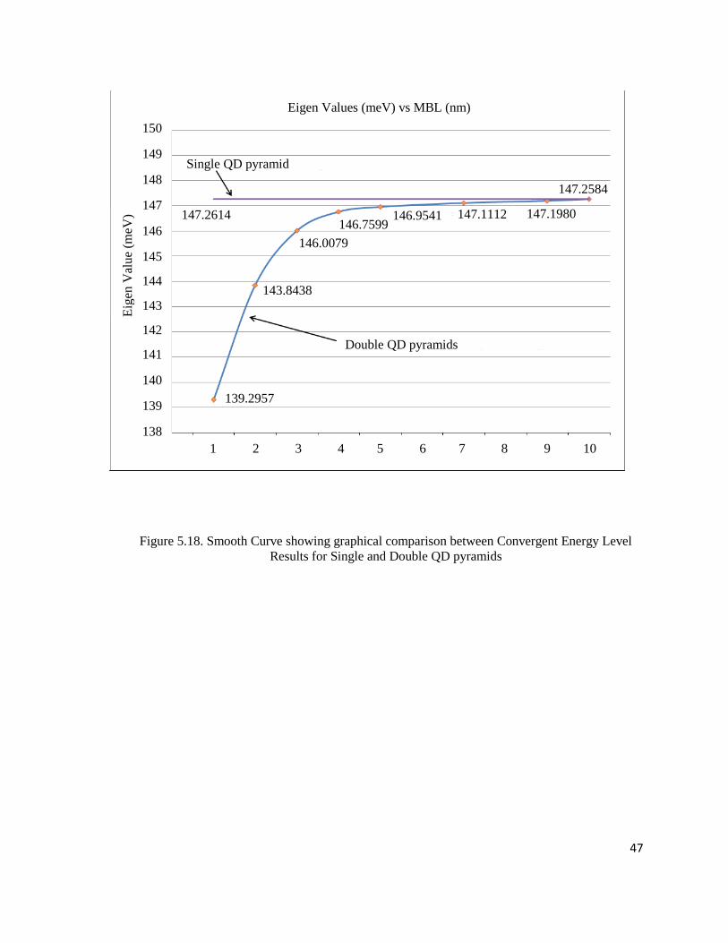
Figure 5.18. Smooth Curve showing graphical comparison between Convergent Energy Level
Results for Single and Double QD pyramids
150
149
148
147
146
145
144
143
142
141
140
139
138
Eig
en V
alu
e (m
eV)
1 2 3 4 5 6 7 8 9 10
Eigen Values (meV) vs MBL (nm)
Single QD pyramid
Double QD pyramids
147.2614
139.2957
143.8438
146.0079
146.7599 146.9541 147.1112 147.1980
147.2584

48
Figure 5.19. Smooth Curves showing graphical comparison between Convergent Energy Level
Code and Published Results (Double QD pyramids)
The smooth curves illustrated above demonstrate the convergence pattern for Double QD
pyramids with increasing MBL. Based on observation from the graph above, as MBL
approaches 9-10 nm, the ground state Eigen value for Double QD pyramids converges
approximately to the ground state Eigen Value for Single QD pyramid. Similar pattern is
also observed for Eigen values generated via implementation of the linear equation
method.
150
149
148
147
146
145
144
143
142
141
140
139
138
Published EVs & Matlab EVs (meV) vs MBL (nm)
0 1 2 3 4 5 6 7 8 9 10 11
Eig
en V
alu
e (m
eV)
150
149
148
147
146
145
144
143
142
141
140
139
138
139.2957
143.8438
146.0079
146.7599
146.9541
147.1112
147.1980
147.2584
Matlab EVs
Published EVs
139.70
144.30
146.40
147.10 147.35
147.50 147.56 147.59
Eig
en V
alue (m
eV)
MBL (nm)

49
5.5. CPU Usage: Strategies for Limited Memory
Although the available CPU memory allocation can easily support computations
involving matrices with respectable sizes, such memory was insufficient for
computations with large matrices with dimensions above 165000 x 165000. However, the
calculation memory can be largely reduced based on the fact that matrix A is a sparse
matrix. The computer performing this computation is equipped with a total of 4 Giga
(109) bytes or GB CPU RAM memory. With such a CPU RAM memory allocation,
simulations involving 563 or 175616 divisions ran for 2 to 3 hours. Meanwhile,
employing 603 or 216000 divisions potentially took several days for computation of
Eigen states. Hence, the number of divisions for simulations was kept less than 56x56x56
for computation of results without compromising the desired values. According to the
latest results, the simulations consumed 1.5 hours on average using 46x46x60 divisions
with uneven division lengths. Overall, by implementing techniques of optimum
combination and uneven divisions in our system, time and memory utilization were kept
under control. The memory consumption was restricted to the allocated limited machine
CPU memory meanwhile simulation time periods were lessened to hours from days
without compromising the overall results. In addition, such techniques paved the way for
more flexibility in selection for combination of divisions along with attaining better
accuracy and convergence for the desired Eigen state results.

50
Chapter 6. Quantum Dot Superlattice
6.1 Solution Procedure
The Schrödinger’s equation that describes the motion of a single hole in QD-SL system
can be written as follows:
The U(r) corresponds to an infinite sequence of quantum dots of size Lx, Ly and Lz
separated by barriers of thickness Hx, Hy and Hz. For our work, the dimensions for both
the quantum dot and barrier sizes were kept as 1-6 nm.
The 3D Schrödinger’s equation decouples into three identical (1D) quantum-well
superlattice equations. The 3D envelope wave function ψ(r) is represented as a product of
three 1D eigenfunctions χ as follows:
The total energy spectrum for this wave function is given by:
where En are eigenvalues of the one-dimensional Schrödinger’s equation.
Finally, the solution for Eq.6.1 is similar to:
)1.6()()(])()(
1
2[
*
2
rErrUrm
rr
)2.6()()()(),,(,,)( zyxzyxr nznynxnznynx
)3.6(nznynxnznynx EEEE
)4.6(,
)sin()sin()(2
1)cos()cos()cos(
0
*
*
*
*
aUEif
HkLkmk
mk
mk
mkHkLkqd WW
WW
BB
BW
WB
BW

51
where
Therefore, the envelope function approximation method is used as mentioned above,
which is also similar to the effective mass method. The Kronig-Penny method is useful
but as mentioned above, this method is limited only to the one dimensional system. The
numerical method based on the envelop function is useful in our case as it is used for the
3D case and it gives more flexibility when solving for superlattice systems.
6.2 Results
Following are results and discussions for the solution of GaAs/InGaAs cubic QDS
structure:
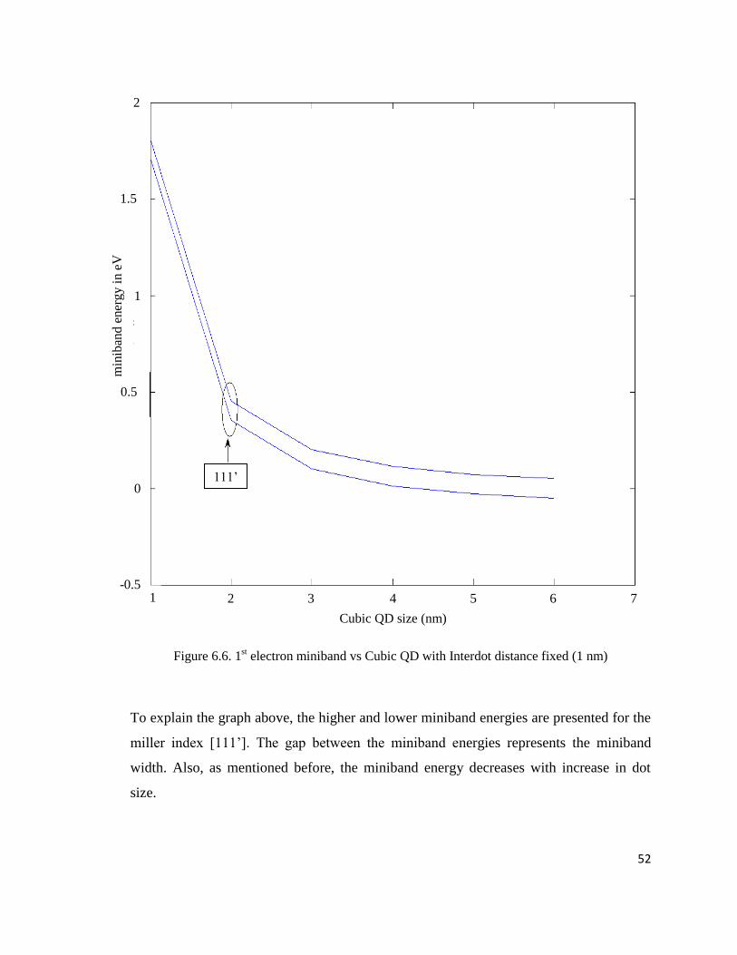
(a). 1st electron miniband vs QD size (1-6 nm) with Interdot distance fixed at 1 nm
Figure 6.6 shows the 1st electron miniband against QD size varying from 1x1x1 nm
3 to
6x6x6 nm3 with interdot distance fixed at 1 nm. Since the highest and lowest bands are
shown in the graph, one can also see the size of the bandgap. Based on observation, as the
QD size within the QDS structure increases, the miniband energy decreases.
)4.6(,0
)sinh()sin()(2
1)cosh()cos()cos(
0
*
*
*
*
bUEif
HkLkmk
mk
mk
mkHkLkqd WW
WW
BB
BW
WB
BW
)5.6(||2
,||2 *
0
*
Emk
UEmk
WWBB
52
Figure 6.6. 1st electron miniband vs Cubic QD with Interdot distance fixed (1 nm)
To explain the graph above, the higher and lower miniband energies are presented for the
miller index [111’]. The gap between the miniband energies represents the miniband
width. Also, as mentioned before, the miniband energy decreases with increase in dot
size.
2
1.5
0.5
1
0
-0.5
min
iban
d e
ner
gy
in
eV
1 2 3 4
Cubic QD size (nm)
5 6 7
111’

53
(b). 1st electron miniband vs Interdot distance (1-6 nm) with QD size fixed at 3 nm
Based on the figure below, the higher and the lower of the energy bands converge at
around 6 nm interdot distance again for the miller index [111’]. Also, the highest
miniband width occurs at interdot distance = 1nm.
Figure 6.7. 1st electron miniband vs Interdot distance with Cubic QD fixed
(c). Density of States vs energy levels
The density of states per unit energy and per unit volume is:
)8.6(|)(|)2(
2)(
3 qE
dSEg
q
E
2
1.5
1
0.5
0
-0.5
Ener
gy (
eV)
Interdot distance (nm)
1 2 3 4 5 6 7
111’
Lower
Higher
Electron Miniband Energy vs Interdot Distance with Cubic QDs sizes fixed

54
The graph generated is presented as follows:
Figure 6.9. Density of States vs energy levels
In the graph above, it is observed that the density of states is high after E = 0.4 eV and at
around E = 1.8 eV. The density of states decays in some region and stays consistent for
enegy values ranging from 1 to 1.6 eV. This pattern can also be observed from the
reference source.

55
Chapter 7. Conclusions & Future Recommendations
In conclusion, we employ the FDM technique to analyze the confined states in the single-
QD and double-QD system. For the single cubic quantum dot, our results agree well with
the analytical solution. In addition, our results also agree well with those published in the
literature for the system comprising of two vertically aligned pyramidal quantum dots.
The discrepancy in the comparison is within 1%. The major concern for using 3D FDM
to solve for quantum confinement structure is the memory usage in the calculation. In
order to compromise between calculation accuracy and memory spending, we used the
optimum divisions along the three spatial dimensions. Along each of the spatial
dimensions, we apply uneven divisions in the quantum dot and barrier matrix regions.
This technique works well systematically for a limited array of QDs. However, the
strategy of implementing FDM does not reflect as a completely effective approach for the
more complex multi-layered QD array structure, which could be solved through different
modeling strategies such as the Kronig-Penney model and the Envelope Function
Approximation.
As far as future recommendations go, structures with more than dual QDs could be tested
with our technique to check the capacity and accuracy of our system for such structures.
After extensive research, many efficient methodologies have been discussed above that
are suitable for multiple arrays of QDs (QD-SL) i.e. the Envelop Function and the
Kronig-Penny models. In addition, programming techniques can be tried from further
exploring the software toolboxes and help pages that might help to utilize less memory
space hence possibly improving the efficiency of the overall system.

56
References
[1] Brus, L.: Quantum crystallites and nonlinear optics. Appl. Phys. A. 53, 465 (1991).
[2] Marti, A., Lopez, N., Antolin, E., Canovas, E., Stanley, C., Farmer, C., Cuadra, L., Luque, A.: Novel
semiconductor solar cell structures: The quantum dot intermediate band solar cell. Thin Solid Films.
511-512 638-644 (2006).
[3] Jiang, C.W and Green, M.A.: Silicon quantum dot superlattices: Modeling of energy bands, densities
of states and mobilities for silicon tandem solar cell applications. J. of Appl. Phys. 99, 114902-1 –
114902-7 (2006).
[4] Norman, A., Hanna, M., Dippo, P., Levi, D., Reedy, R., Ward, J., Al-Jassim, M.: InGaAs/GaAs QD
Superlattices: MOVPE Growth, Structural and Optical Characterization, and Application in
Intermediate-Band Solar Cells. NREL/CP 520-37405 (2005).
[5] Li, T., Kuhn, K.: Finite Element Solutions to GaAs-AlAs Quantum Wells with Connection Matrices
at Heterojunctions. J. of Comp. Phys. 115, 2, 288-295 (1994).
[6] Zhou, S., Rui, W., Shuang, C., Hao, C.: Finite Difference Time Domain Modeling of Grating-Coupled
Quantum Well Infrared Photodetector. J. Infrared Millim. Waves. 23, 6 (2004).
[7] Hughes, S.: High-field wave packets in semiconductor quantum wells: A real-space finite-difference
time-domain formalism. Phys. Rev. B 69, 205308 (2004).
[8] Wikipedia Inc.: Quantum Dot. http://en.wikipedia.org/wiki/Quantum_dot. Accessed July 2009.
[9] Reed, M.: Quantum Dots. Scientific American. 268, 118 (1993).
[10] Brus, L.: Chemistry and Physics of Semiconductor Nanocrystals. Columbia University (2007).
[11] Murray, C., Kagan, C., Bawendi, M.: Synthesis and characterization of monodisperse nanocrystals
and close-packed nanocrystal assemblies. Annu. Rev. Mater. Sci. 30, 545-610 (2000).
[12] Norris, J.: Measurement and Assignment of the size-dependent optical spectrum in cadmium selenide
(CdSe) Quantum Dots. Massachusetts Institute of Technology (1995).
[13] Kouwenhoven, P., Marcus, M., Mceuen, L., Tarucha, S., Westervelt, M., Wingreen, S.: Electron
Transport in Quantum Dots. Mesoscopic Electron Transport (1997).
[14] Watson, A., Wu, X., Bruchez, M.: Lighting up cells with quantum dots. Biotechniques. 24, 296-300,
302-303 (2003).
[15] Halliday, D., Resnick, R., Walker, J.: Fundamentals of Physics. Science. 6, (2002).
[16] Takagahara, T., Takeda, K.: Theory of Quantum confinement effect on excitons in quantum dots of
indirect-gap materials. Phys. Rev. B 46, 15578 – 15581 (1992).
[17] Klimov, V.: Nanocrystal Quantum Dots. Los Alamos Science. 214 (2003).
[18] Bimberg, D., Kirstaedter, N., Ledentsov, N., Alferov, Zh., Kop’ev, P., Ustinov, V.: InGaAs-GaAs
Quantum-Dot Lasers. IEEE J. of Sel. Topics in Quan. Mech. 3, 2 (1997).
[19] Pathak, S., Elizabeth, C., Davidson, M., Jin, S., Silva, G.: Quantum Dot Applications to

57
Neuroscience: New Tools for Probing Neurons and Glia. The Journal of Neuroscience. 26(7):1893-
1895 (2006).
[20] Jaiswal, J., Mattoussi, H., Mauro, J., Simon, S.: Long-term multiple color imaging of live cells using
quantum dot bioconjugates. Nat Biotechnol. 21, 47-51 (2003).
[21] Michalet, X., Pinaud, F., Bentolila, L., Tsay, J., Doose, S., Li, J., Sundaresan, G., Wu, A., Gambhir,
S., Weiss, S.: Quantum dots for live cells, in vivo imaging, and diagnostics. Science. 307, 538-544
(2005).
[22] Terpetschnig, E.: Fluorescence Probes and Labels for Biomedical Applications.
http://www.fluorescence-foundation.org/lectures/chicago2009/lecture10.pdf. Accessed October
2009.
[23] Xiao, Y., Barker, P.: Semiconductor nanocrystal probes for human metaphase chromosomes. Nucleic
Acids Res. 32(3) e28 (2004).
[24] Alivasatos, P.: Semiconductor clusters, nanocrystals and quantum dots. Science. 271, 933-937
(1996).
[25] Nirmal, M., Brus, L.: Luminescence photophysics in semiconductor nanocrystals. Acc. Chem. Res.
32, 407-414 (1999).
[26] Klein, M., Levine, R., Remacle, F.: Principles of design of a set-reset finite state logic nanomachine.
J. Appl. Phys. 104, 044509 (2008).
[27] Lent, C., Tougaw, P., Porod, W.: Quantum cellular automata: the physics of computing with
arrays of quantum dot molecules, in Proceedings of the Workshop on Physics and Computation
(PhysComp '94), IEEE. Computer Society Press, 5-13 (1994).
[28] Kemerink, M., Molenkamp, L.: Stochastic Coulomb blockade in a double quantum dot. Appl.
Phys. Lett. 65, 10 12- 1014 (1994).
[29] Behrman, E., Niemel, J., Steck, J., Skinner, S.: A Quantum Dot Neural Network. Proceedings of the
4th Workshop on Physics of …., Citeseer (1996).
[30] Takata, M., Kondoh, S., Sakaguchi, T., Choi, H., Shim, J., Kurino. H., Koyanagi, M.: New Non-
Volatile Memory with Extremely High Density Metal Nano-Dots. IEEE. IEDM 03-553 (2003).
[31] Coe, S., Woo, W., Bawendi, M., Bulovi , V.: Electroluminescence from single monolayers of
nanocrystals in molecular organic devices. Nature. 420, 800-803 (2002).
[32] Narukawa, Y., Kawakami, Y., Funato, M., Fujita, S., Fujita, S., Nakamura, S.: Role of self-formed
InGaN quantum dots for exciton localization in the purple laser diode emitting at 420 nm. Appl.
Phys. Lett. 70, 981 (1997);
[33] Tamura, H., Shiraishi, K., Kimura, T., Takayanagi, H.: Flat-band ferromagnetism in quantum dot
superlattices. Phys. Rev. B 65 085324 (2002).
[34] Tamura, H., Shiraishi, K., Takayanagi, H.: Theoretical design of a semiconductor ferromagnet based

58
on quantum dot superlattices. Physica. E 24 107-110 (2004).
[35] Lazarenkova, O. and Baladin, A.A.: Miniband formation in quantum dot crystal. J. of Appl. Phys. 89,
5509-5515 (2001).
[36] Murray, C., Kagan, C., Bawendi, M.: Self-Organization of CdSe Nanocrystallites into three-
dimensional quantum dot superlattices. Science. 270, 1335-1338 (1995).
[37] Yang, Z., Shi, Y., Liu, J., Yan, B., Zhang, R., Zheng, Y., Wang, K.: Optical Properties Ge/Si
quantum dot superlattices. Materials Letters. 58, 3765–3768 (2004).
[38] Chen, J., Markus, A., Fiore, A., Oesterle, U., Stanley, R., Carlin, J., Houdre´, R., Ilegems, M.,
Lazzarini, L., Nasi, L., Todaro, M., Piscopiello, E., Cingolani, R., Catalano, M., Katcki, J.,
Ratajczak, J.: Tuning InAsÕGaAs quantum dot properties under Stranski-Krastanov growth mode for
1.3 mm applications. J. of Appl. Phys. 91, 6710-6716 (2002).
[39] Petroff, P., DenBaars, S.: MBE and MOCVD Growth and Properties of Self-Assembling Quantum
Dot Arrays in III-V Semiconductor Structures. Superlattices and Microstructures. 15, 15-21 (1994).
[40] Takagahara, T.: Quantum dot lattice and enhanced excitonic optical nonlinearity. Surf. Sci. 267, 310-
314 (1992).
[41] Liu, H., Sionnest, P.: Infrared Fluorescence of Lead Selenide Colloidal Quantum Dots.
http://hep.uchicago.edu/cdf/frisch/p335/feb6_liu.pdf. Accessed October 2009.
[42] Heitmann, D., Kotthaus, J.: Spectroscopy of quantum dot arrays. Phys. Today. 46, 56-63 (1993).
[43] Tersoff, J., Teichert, C., Lagally, M.: Self-Organization in Growth of Quantum Dot Superlattices.
Phys. Rev. Lett. 76, 10, 1675-1678 (1996).
[44] Kuan, T., Iyer, S.: Strain relaxation and ordering in SiGe layers grown on (100), (111), and (110) Si
surfaces by molecular-beam epitaxy. Appl. Phys. Lett. 59, 18, 2242-2244 (1991).
[45] Yao, J., Andersson, T., Dunlop, G.: The interfacial morphology of strained epitaxial InxGa1-xAs /
GaAs. J. Appl. Phys. 69, 4, 2224-2230 (1991).
[46] Xie, Q., Madhukar, A., Chen, P., and Kobayashi., N.: Vertically Self-Organized InAs Quantum Box
Islands on GaAs (100). Phys. Rev. Lett. 75, 2542-2545 (1995).
[47] Solomon, G., Trezza, J., Marshall, A., and Harris, J.Jr..: Vertically Aligned and Electronically
Coupled Growth Induced InAs Islands in GaAs. Phys. Rev. Lett. 76, 952-955 (1996).
[48] Harman, T., Taylor, P., Walsh, M., LaForge, B.: Quantum Dot Superlattice Thermoelectric Materials
and Devices. Science. 297, 27, 2229-2232 (2002).
[49] Harman, T., Taylor, P., Spears, D., Walsh, M.: Thermoelectric Quantum-Dot Superlattices with High
ZT. J. Electron. Mater. 29, L1 (2000).
[50] _______, in 18th International Conference on Thermoelectrics: ICT Symposium Proceedings,
Baltimore, MD (IEEE, Piscataway, NJ), 280–284 (1999).
[51] Dresselhaus, M. in Recent Trends in Thermoelectric Materials Research III, Semiconductors and
Semimetals, Tritt, T., vol. Ed, Willardson, R., Weber, E. series Eds. (Academic Press, London). 71,

59
chap.1 (2001).
[52] Moghraby, D.E., Johnson, R.G. and Harrison, P.: The effect of inter-dot separation on the finite
difference solution of vertically aligned coupled quantum dots. Computer Phys. Communications.
155, 236-243 (2003).
[53] Hwang, T.M., Lin, W.W., Wang, W.C. and Wang, W.: Numerical simulation of three dimensional
pyramid quantum dot. J. of Computational Phys. 196, 208-232 (2004).
[54] Moghraby, D.E., Johnson, R.G. and Harrison, P.: Calculating models of quantum wire and dot
systems using a finite differencing technique. Computer Phys. Communications. 150, 235-246
(2003).
[55] Brennan, K.: The Physics of Semiconductors. Cambridge University Press (1999).
[56] Wikipedia Inc.: Schrödinger Equation. http:// en.wikipedia.org/wiki/Schrödinger_equation. Accessed
July 2009.
[57] Nave, C.R.: 3-D Schrodinger Equation. HyperPhysics, Physics & Astronomy Dept., Georgia State
University.
http://hyperphysics.phy-astr.gsu.edu/hbase/quantum/sch3D.html. Accessed August 2008.
[58] Griffiths, D.J.: Introduction to Quantum Mechanics. Prentice Hall Inc (1995).
[59] Harrison, P.: Quantum Wells, Wires and Dots: Theoretical and Computational Physics of
Semiconductor Nanostructures. John Wiley & Sons LTD (2007).
[60] Poe, C.: Schrodinger’s Equation. Physics Department, Mission College.
http://www.missioncollege.org/depts/physics/P4poe/P4D/Schrodinger.htm. Accessed August 2008.
[61] Kuzmin, D.: Finite Difference Method. Institute of Applied Mathematics, University of Dortmund.
http://www.mathematik.uni-dortmund.de/~kuzmin/cfdintro/lecture4.pdf. Accessed July 2008.
[62] The Mathworks.: MATLAB: The Language of Technical Computing. The Mathworks, Inc. (2000).
[63] Wikipedia Inc.: Finite Difference Method. http://en.wikipedia.org/wiki/Finite_difference_method.
Accessed July 2008.