computer architectures - cvut.cz
TRANSCRIPT

AE0B36APO Computer Architectures
Czech Technical University in Prague, Faculty of Electrical Engineering
Computer Architectures
Ver.1.00
Processor+Memory Richard Šusta, Pavel Píša
2019 1

2 AE0B36APO Computer Architectures
The main instruction cycle of the CPU
1. Initial setup/reset – set initial PC value, PSW, etc.
2. Read the instruction from the memory
PC → to the address bus
Read the memory contents (machine instruction) and transfer it to the IR
PC+l → PC, where l is length of the instruction
3. Decode operation code (opcode)
4. Execute the operation
compute effective address, select registers, read operands, pass them through ALU and store result
5. Check for exceptions/interrupts (and service them)
6. Repeat from the step 2

Single cycle CPU – implementation of the load instruction
B35APO Computer Architectures 3
PC’ PC Instr 25:21
15:0
SrcA
SrcB
Zero
AluOut
SignImm
ReadData
Instr.
Memory
A RD
Data
Memory
A RD
WD
WE
Reg.
File
A1 RD1
A2 RD2
A3
WD3
WE3
Sign Ext
ALU
I opcode(6), 31:26 rs(5), 25:21 rt(5), 20:16 immediate (16), 15:0
ALUControl
lw: type I, rs – base address, imm – offset, rt – register where to store fetched data

Single cycle CPU – implementation of the load instruction
B35APO Computer Architectures 4
PC’ PC Instr 25:21
20:16
15:0
SrcA
SrcB
Zero
AluOut
SignImm
ReadData
Instr.
Memory
A RD
Data
Memory
A RD
WD
WE
Reg.
File
A1 RD1
A2 RD2
A3
WD3
WE3
Sign Ext
ALU
I opcode(6), 31:26 rs(5), 25:21 rt(5), 20:16 immediate (16), 15:0
ALUControl RegWrite = 1
Write on rising edge of CLK
lw: type I, rs – base address, imm – offset, rt – register where to store fetched data

PC’
Single cycle CPU – implementation of the load instruction
B35APO Computer
Architectures
5
PC Instr 25:21
20:16
15:0
SrcA
SrcB
Zero
AluOut
SignImm
ReadData
Instr.
Memory
A RD
Data
Memory
A RD
WD
WE
Reg.
File
A1 RD1
A2 RD2
A3
WD3
WE3
Sign Ext
ALU
I opcode(6), 31:26 rs(5), 25:21 rt(5), 20:16 immediate (16), 15:0
ALUControl RegWrite = 1
4
+
PCPlus4
lw: type I, rs – base address, imm – offset, rt – register where to store fetched data

20:16
PC’
Single cycle CPU – implementation of the store instruction
B35APO Computer Architectures 6
PC Instr 25:21
20:16
15:0
SrcA
SrcB
Zero
AluOut
SignImm
ReadData
Instr.
Memory
A RD
Data
Memory
A RD
WD
WE
Reg.
File
A1 RD1
A2 RD2
A3
WD3
WE3
Sign Ext
ALU
I opcode(6), 31:26 rs(5), 25:21 rt(5), 20:16 immediate (16), 15:0
ALUControl RegWrite = 0
4
+
MemWrite = 1
PCPlus4
sw: type I, rs – base address, imm – offset, rt – select register to store into memory

Switch analogy
B35APO Computer Architectures 7
Select
x0
x1
1
0
z
1bit Select (address)
x0
x1
z
Multiplexer 2 to 1
PC’
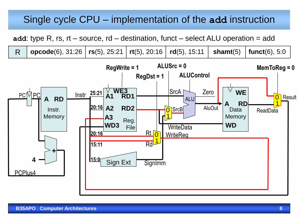
Single cycle CPU – implementation of the add instruction
B35APO Computer Architectures 8
R opcode(6), 31:26 rs(5), 25:21 rt(5), 20:16 rd(5), 15:11 shamt(5) funct(6), 5:0
20:16
4
PC Instr 25:21
20:16
15:11
15:0
SrcA
SrcB
Zero
AluOut
WriteData WriteReg
SignImm
ReadData
Result
PCPlus4
Rt
Rd
Instr.
Memory
A RD
Data
Memory
A RD
WD
WE
Reg.
File
A1 RD1
A2 RD2
A3
WD3
WE3
+
0 1
0 1
0 1
Sign Ext
ALU
RegWrite = 1
RegDst = 1
ALUSrc = 0 MemToReg = 0 ALUControl
add: type R, rs, rt – source, rd – destination, funct – select ALU operation = add

PC’
Single cycle CPU – sub, and, or, slt
B35APO Computer Architectures 9
20:16
4
PC Instr 25:21
20:16
15:11
15:0
SrcA
SrcB
Zero
AluOut
WriteData WriteReg
SignImm
ReadData
Result
PCPlus4
Rt
Rd
Instr.
Memory
A RD
Data
Memory
A RD
WD
WE
Reg.
File
A1 RD1
A2 RD2
A3
WD3
WE3
+
0 1
0 1
0 1
Sign Ext
ALU
RegWrite = 1
RegDst = 1
ALUSrc = 0 MemToReg = 0 ALUControl
Only difference is another ALU operation selection (ALUcontrol). The data path is the same as for add instruction

20:16
4
PC’ PC Instr 25:21
20:16
15:11
15:0
SrcA
SrcB
Zero
AluOut
WriteData WriteReg
SignImm PCBranch
ReadData
Result
PCPlus4
Rt
Rd
Instr.
Memory
A RD
Data
Memory
A RD
WD
WE
Reg.
File
A1 RD1
A2 RD2
A3
WD3
WE3
+
+
0 1
0 1
0 1
0 1
Sign Ext <<2
ALU
• beq – branch if equal; imm–offset; PC´ = PC+4 + SignImm*4
Single cycle CPU – implementation of beq
B35APO Computer Architectures 10
I opcode(6), 31:26 rs(5), 25:21 rt(5), 20:16 immediate (16), 15:0
RegWrite = 0
RegDst = x
ALUSrc = 0 MemToReg = x ALUControl
Branch = 1

• What is the maximal possible frequency of the CPU?
• It is given by latency on the critical path – it is lw instruction in our case:
Tc = tPC + tMem + tRFread + tALU + tMem + tMux + tRFsetup
Single cycle CPU – Throughput: IPS = IC / T = IPCstr
.fCLK
B35APO Computer Architectures 11
PC’ Result
SrcB
15:0
25:21 PC
4
Instr
20:16
20:16
15:11
SrcA Zero
AluOut
WriteData WriteReg
SignImm PCBranch
ReadData
PCPlus4
Rt
Rd
Instr.
Memory
A RD
Data
Memory
A RD
WD
WE
Reg.
File
A1 RD1
A2 RD2
A3
WD3
WE3
+
+
0 1
0 1
0 1
0 1
Sign Ext <<2
ALU

Single cycle CPU – Throughput: IPS = IC / T = IPCstr
.fCLK
• Tc = Tcinstr + Tcproc
= (tPC + tMem) + (tRFread + tALU + tMem + tMux + tRFsetup)
• Consider following parameters:
tPC = 30 ns tMem = 300 ns
tRFread = 50 ns tALU = 200 ns
tMux = 20 ns tRFsetup = 20 ns
Then Tc = 920 ns --> fCLK max = 1,08 MHz,
IPS = 1 080 000 [instructions per second]
B35APO Computer Architectures 12
If Tcinstr is executed paralel with Tcproc,
then Tci < Tcp, and Tcp = 50+200+300+20+20
= 590 ns = 1.69 MHz -> IPS = 1 690 000

Note
• Remember the result, so you can compare
it with result for pipelined CPU.
B35APO Computer Architectures 13

Key Technology Gaps Prediction
B35APO Computer Architectures 14
Note: The increase of algorithm complexity over time has been formalized in literature with
the so-defined Shannon's law.

Memory and CPU speed – Moore's law
B35APO Computer Architectures 15
more exact numbers
CPU performance
25% per year
52% per year
20% per year
Processor-Memory Performance Gap Growing
Throughput of memory
only +7% per year
Source: Hennesy, Patterson CaaQA 4th ed. 2006

Layout of a Program in Memory
Stack Segment
(cz:zásobník)
Dynamic Area, heap
(cz: halda)
Static Initialized Data
Text Segment
Other programs
Data Segment
Stack grows
to lower address
Static Uninitialized Data
.ent start
entry point,
initial value of PC
Heap grows
to higher address
lower address
higher address
B35APO Computer Architectures

Memory Addressing
Memory address in load and store instructions is
specified by a base register and offset
This is called base addressing
addi a0, zero, 10 // load the word from absolute address
lw $2, 0x2000($0) // store the word to absolute address
sw $2, 0x2004($0)

Data Types in Instructions
MIPS registers hold 32-bit (4-byte) words.
Byte = 8 bits - example: lb / lbu
- load byte extend signed/unsigned
Halfword = 2 bytes example: - lh / lhu
- load halfword extend signed/unsigned
Other common data sizes include byte and halfword.
Word = 4 bytes - example: - lw - load word
u-unsigned extension 18
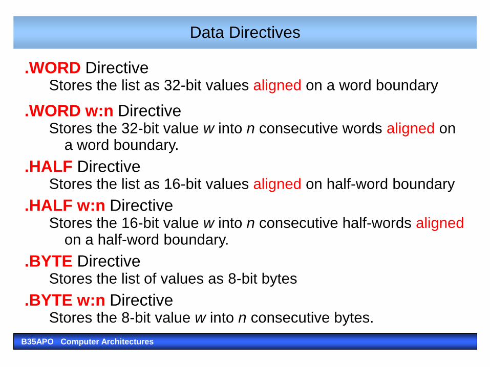
Data Directives
.WORD Directive Stores the list as 32-bit values aligned on a word boundary
.WORD w:n Directive Stores the 32-bit value w into n consecutive words aligned on
a word boundary.
.HALF Directive Stores the list as 16-bit values aligned on half-word boundary
.HALF w:n Directive Stores the 16-bit value w into n consecutive half-words aligned
on a half-word boundary.
.BYTE Directive Stores the list of values as 8-bit bytes
.BYTE w:n Directive Stores the 8-bit value w into n consecutive bytes.
B35APO Computer Architectures

String Directives
.ASCII Directive
Allocates a sequence of bytes for an ASCII string
.ASCIIZ Directive
Same as .ASCII directive, but adds a NULL char at end of string
Strings are null-terminated, as in the C programming language
.SPACE n Directive
Allocates space of n uninitialized bytes in the data segment
Special characters in strings follow C convention
Newline: \n Tab:\t Quote: \”
B35APO Computer Architectures

Memory Alignment
.align n directive
- aligns the next data definition begins on a 2n byte boundary
.align 2
- the least significant 2 bits of address should be 00
Memory is addressed as an array of bytes
Words occupy 4 consecutive bytes (MIPS is 32bit processor),
0
4
8
12
ad
dre
ss
not aligned
. . .
aligned word
not aligned
Memory
B35APO Computer Architectures

Address 0 1 2 3 4 5 6 7 8 9 A B C D E F
0x2000 3 5 41 50 4F 12 34 56 78
0x2010 10 00
Assembler align data in data segment
.DATA
.ALIGN 2
var1: .BYTE 3, 5,'A','P','O'
var2: .WORD 0x12345678
.ALIGN 3
var3: .HALF 1000
Align
var1 var2
var3
Example on BIG ENDIAN
B35APO Computer Architectures

23 B35APO Computer Architectures
Lecture motivation
A: int matrix[M][N];
int i, j, sum = 0;
…
for(i=0; i<M; i++)
for(j=0; j<N; j++)
sum += matrix[i][j];
Quick Quiz 1.: Is the result of both code fragments a same?
Quick Quiz 2.: Which of the code fragments is processed faster and why?
B: int matrix[M][N];
int i, j, sum = 0;
…
for(j=0; j<N; j++)
for(i=0; i<M; i++)
sum += matrix[i][j];
Is there a rule how to iterate over matrix element efficiently?

PC Computer Motherboard
B35APO Computer Architectures 24
http://www.pcplanetsystems.com/abc/product_details.php?item_id=3263&category_id=208

Computer architecture (desktop x86 PC)
B35APO Computer Architectures 25
generic example

From UMA to NUMA development (even in PC segment)
B35APO Computer Architectures 26
CPU 1 CPU 2
Northbridge
MC
Southbridge
RAM
MC - Memory controller – contains circuitry responsible for SDRAM read and writes. It also
takes care of refreshing each memory cell every 64 ms.
CPU 1 CPU 2
MC
Southbridge
RAM
RAM
MC Northbridge
Southbridge
USB PCI-E
CPU 1 CPU 2
MC MC
RAM RAM
Non-Uniform Memory
Architecture
SATA
USB PCI-E SATA
USB PCI-E SATA
Southbridge
USB PCI-E
CPU 1 CPU 2
MC
RAM RAM
SATA

Intel Core 2 generation
B35APO Computer Architectures 27

Intel i3/5/7 generation
B35APO Computer Architectures 28

Memory subsystem – terms and definitions
B35APO Computer Architectures 29
● Memory address – fixed-length sequences of bits or index
● Data value – the visible content of a memory location
● Memory location can hold even more control/bookkeeping information
● validity flag, parity and ECC bits etc.
Basic memory parameters:
● Access time – delay or latency between a request and the access
being completed or the requested data returned
● Memory latency – time between request and data being available
(does not include time required for refresh and deactivation)
● Throughput/bandwidth – main performance indicator. Rate of
transferred data units per time.
● Maximal, average and other latency parameters

Internal architecture of the DRAM memory chip
B35APO Computer Architectures 30
This 4M × 1 DRAM (Dynamic Random Access Memory)
is internally realized as an 2048x2048 array of 1b memory cells

Memory Cell
stored
bit = 1
bitline =1
row-address
1
stored
bit = 0
row-address
1
bitline =0
stored
bit = 0
row-address
= 0
bitline =Z
stored
bit = 1
row-address
= 0
bitline =Z
stored
bit
row-address
bitline
B35APO Computer Architectures

Switch Analogy of Decoder
y y
1
0
3
2
1 0
x 0
x 3
x 2
x 1
32
y1 y0 x
0
x 3
x 2
x 1 '1'
One Hot Decoder cz: Dekodér 1 ze 4
B35APO Computer
Architectures
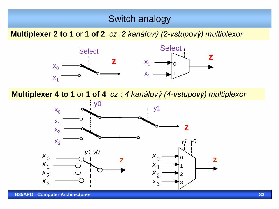
Switch analogy
B35APO Computer Architectures 33
x 0
x 3
x 2
x 1 1
0
3
2
y1 y0
y1 y0 x
0
x 3
x 2
x 1
z z
Select
x0
x1
1
0
z Select
x0
x1
z
y0 x0
x1
x2
x3
y1
z
Multiplexer 4 to 1 or 1 of 4 cz : 4 kanálový (4-vstupový) multiplexor
Multiplexer 2 to 1 or 1 of 2 cz :2 kanálový (2-vstupový) multiplexor
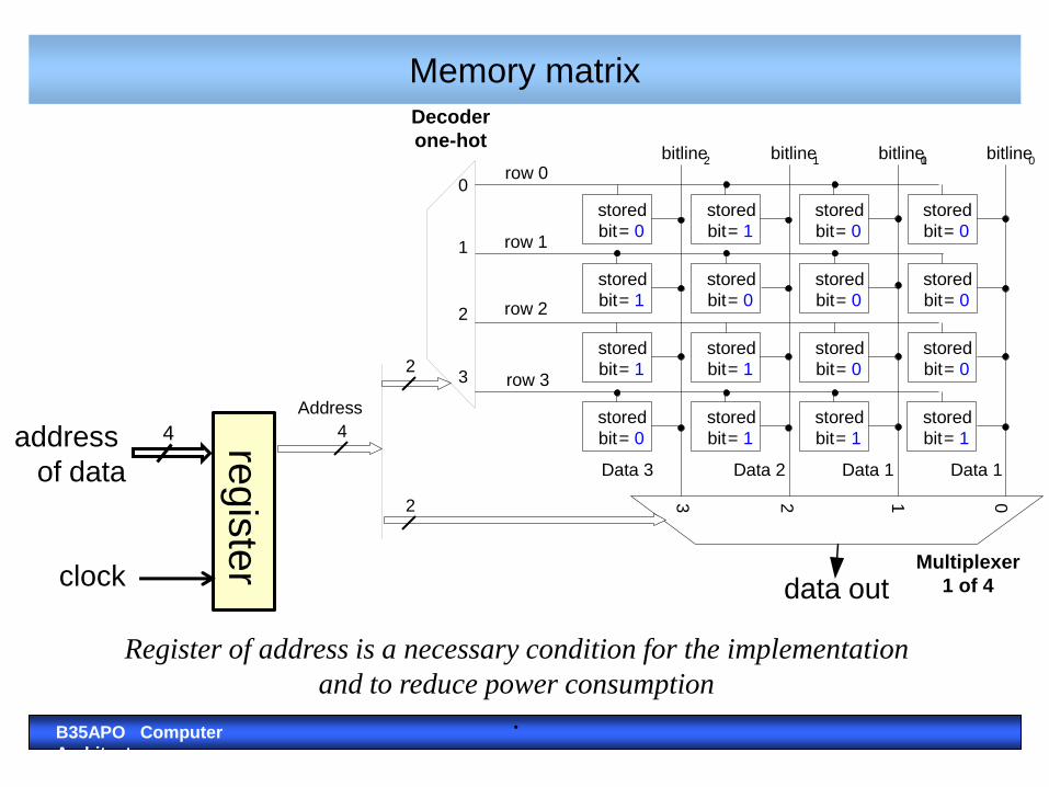
Memory matrix
data out
4
clock
regis
ter
address
of data
Register of address is a necessary condition for the implementation
and to reduce power consumption
.
row 0
Decoder
one-hot
Address
stored
bit = 0row 1
row 2
row 3
stored
bit = 1
stored
bit = 0
stored
bit = 1
stored
bit = 0
stored
bit = 0
stored
bit = 1
stored
bit = 1
stored
bit = 0
stored
bit = 0
stored
bit = 1
stored
bit = 1
bitline2 bitline1 bitline0
Data 3
2
stored
bit = 0
stored
bit = 0
stored
bit = 0
stored
bit = 1
1 bitline0
Data 2 Data 1 Data 1
3
2
1
0
3 2 1 02
4
Multiplexer
1 of 4
B35APO Computer
Architectures

Memory matrix - example 1/4
clock
regis
ter
Address value is waiting for the rising edge of clocks
address
6 = 0110
row 0
Decoder
one-hot
Address
stored
bit = 0row 1
row 2
row 3
stored
bit = 1
stored
bit = 0
stored
bit = 1
stored
bit = 0
stored
bit = 0
stored
bit = 1
stored
bit = 1
stored
bit = 0
stored
bit = 0
stored
bit = 1
stored
bit = 1
bitline2 bitline1 bitline0
Data 3
2
stored
bit = 0
stored
bit = 0
stored
bit = 0
stored
bit = 1
1 bitline0
Data 2 Data 1 Data 1
3
2
1
0
3 2 1 02
4
Multiplexer
1 of 4
B35APO Computer
Architectures

Memory matrix - example 2/4
clock
regis
ter
address
6 = 0110
Address was loaded on the rising edge of clocks
and divided to two parts, higher and lower bits
row 0
Decoder
one-hot
0110
stored
bit = 0row 1
row 2
row 3
stored
bit = 1
stored
bit = 0
stored
bit = 1
stored
bit = 0
stored
bit = 0
stored
bit = 1
stored
bit = 1
stored
bit = 0
stored
bit = 0
stored
bit = 1
stored
bit = 1
bitline2 bitline1 bitline0
Data 3
01
stored
bit = 0
stored
bit = 0
stored
bit = 0
stored
bit = 1
1 bitline0
Data 2 Data 1 Data 1
3
2
1
0
3 2 1 0
Multiplexer
1 of 4
10
B35APO Computer
Architectures

Memory matrix - example 3/4
clock
regis
ter
address
6 = 0110
Output of one-hot decoder 1 from N aktivate row
and of cell in it.
row 0
Decoder
one-hot
0110
stored
bit = 0row 1
row 2
row 3
stored
bit = 1
stored
bit = 0
stored
bit = 1
stored
bit = 0
stored
bit = 0
stored
bit = 1
stored
bit = 1
stored
bit = 0
stored
bit = 0
stored
bit = 1
stored
bit = 1
bitline2 bitline1 bitline0
Data 3
01
stored
bit = 0
stored
bit = 0
stored
bit = 0
stored
bit = 1
1 bitline0
Data 2 Data 1 Data 1
3
2
1
0
3 2 1 0
Multiplexer
1 of 4
10
B35APO Computer
Architectures
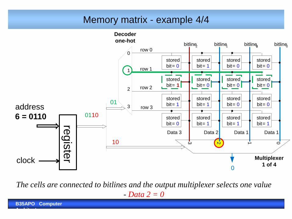
Memory matrix - example 4/4
clock
regis
ter
address
6 = 0110
The cells are connected to bitlines and the output multiplexer selects one value
- Data 2 = 0
row 0
Decoder
one-hot
0110
stored
bit = 0row 1
row 2
row 3
stored
bit = 1
stored
bit = 0
stored
bit = 1
stored
bit = 0
stored
bit = 0
stored
bit = 1
stored
bit = 1
stored
bit = 0
stored
bit = 0
stored
bit = 1
stored
bit = 1
bitline2 bitline1 bitline0
Data 3
01
stored
bit = 0
stored
bit = 0
stored
bit = 0
stored
bit = 1
1 bitline0
Data 2 Data 1 Data 1
3
2
1
0
Multiplexer
1 of 4
10
0
3 2 1 0
B35APO Computer
Architectures
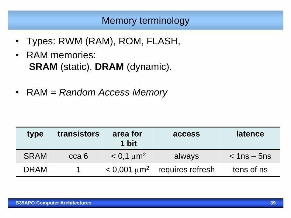
Memory terminology
• Types: RWM (RAM), ROM, FLASH,
• RAM memories:
SRAM (static), DRAM (dynamic).
• RAM = Random Access Memory
B35APO Computer Architectures 39
type transistors area for
1 bit
access latence
SRAM cca 6 < 0,1 m2 always < 1ns – 5ns
DRAM 1 < 0,001 m2 requires refresh tens of ns

Typical chip and SRAM cell
B35APO Computer Architectures 40
Area of cell:
SRAM cell 6-transistors CMOS, but there are also 4 transistors versions
Principle:
http://educypedia.karadimov.info/library/SEC08.PDF
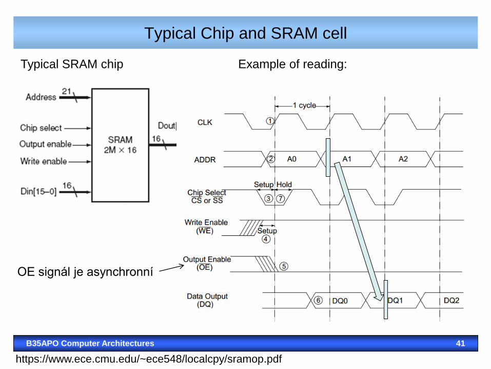
Typical Chip and SRAM cell
B35APO Computer Architectures 41
Typical SRAM chip Example of reading:
https://www.ece.cmu.edu/~ece548/localcpy/sramop.pdf
OE signál je asynchronní

Typical Chip and SRAM cell
B35APO Computer Architectures 42
Bigger memory?

Dynamic memory cell detail
B35APO Computer Architectures 43
Single transistor dynamic memory
cell
The nMOS transistor is a switch that connects (or not) a capacitor to a
"bitline" wire. The connection is controlled by the wordline wire.
Obrázek: http://www.eetimes.com/document.asp?doc_id=1281315

Capacitor
B35APO Computer Architectures 44
Commercial DRAM parameters
Capacity fF [femtofarad]
Storage capacitor from 10 fF to 50 fF
Bit line around 2 fF
[Source: l'INSA de Toulouse]
fF - femtofarad
An SI unit of electrical capacitance equal to 10−15 farads.
10-6 F = 1 μF = 103 nF = 106 pF = 109 fF
~9 fF - the capacitor is created by two 1 mm2 plates
in 1 mm distance inside vacuum

Development of DRAM chips in time
B35APO Computer Architectures 45
Year Capacity Price[$]/GB Access time [ns]
1980 64 Kb 1 500 000 250
1983 256 Kb 500 000 185
1985 1 Mb 200 000 135
1989 4 Mb 50 000 110
1992 16 Mb 15 000 90
1996 64 Mb 10 000 60
1998 128 Mb 4 000 60
2000 256 Mb 1 000 55
2004 512 Mb 250 50
2007 1 Gb 50 40
RAS – Row Address Strobe,
CAS – Column Address Strobe

Classical DRAM - asynchronous interface
• The address is transferred in two phases – reduces
number of chip module pins and is natural for internal
DRAM organization
• This method is preserved even for today chips
B35APO Computer Architectures 46
RAS – Row Address Strobe,
CAS – Column Address Strobe
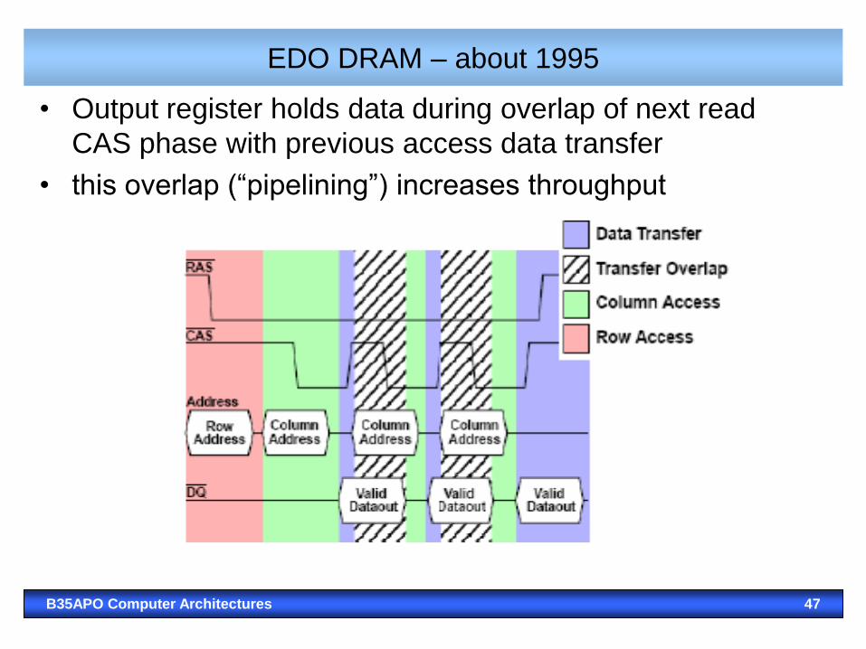
EDO DRAM – about 1995
B35APO Computer Architectures 47
• Output register holds data during overlap of next read
CAS phase with previous access data transfer
• this overlap (“pipelining”) increases throughput

SDRAM – konec 90.let – synchronní DRAM
SDRAM chip is equipped by counter that can be used to define
continuous block length (burst) which is read together.
B35APO Computer Architectures 48

Consecutive Read/Write
B35APO Computer Architectures 49

From SDRAM to Contemporary mMemories
• SDRAM – clock frequency up to 100 MHz, 2.5V
• DDR (double data rate) SDRAM – data transfer at both CLK edges,
2.5V, I/O bus clock 100-200 MHz,
speed 0.2-0.4 GT/s (gigatransfers per second)
• DDR2 SDRAM – lower power consumption by power 1.8V,
frequency of IO bus 400 MHz, 0.8 GT/s
• DDR3 SDRAM – lower power consumption by power 1.5V, IO bus
frequency up to 800 MHz, 1.6 GT/s
• DDR4 SDRAM - 1.05 – 1.2V, I/O bus clock 1.2 GHz, 2.4 GT/s
• DDR5 SDRAM - expected during 2019-20,
supposed transfer rate ~6 GT/s
B35APO Computer Architectures 50
All these innovations are focused mainly on throughput,
not on the random access latency.
Other Memories
• QDRx SDRAM (Quad Data Rate) - however, they are not 2 * faster,
they only allow simultaneous read and write since they have separate
clocks for RD and WR, while DDRs are more efficient than QDR for
one type of access.
• GDDR SDRAM - today up to GDDR6, suitable for graphics cards -
based on DDR memory.
- their speed is accelerated by the extended output bus.
• Furthermore, there are memories and RDRAM modules (RAMBUS
DRAMs), which have a completely different interface and method of
use. For patent litigation, they have not been used in personal
computers since 2003.
B35APO Computer Architectures 51