computer structure pc structure and peripherals
DESCRIPTION
Computer Structure PC Structure and Peripherals. Lihu Rappoport and Adi Yoaz. Hard Disks. Platters. Hard Disk Structure. Rotating platters coated with a magnetic surface Each platter is divided to tracks: concentric circles Each track is divided to sectors - PowerPoint PPT PresentationTRANSCRIPT
Computer Structure 2013 – PC Structure and Peripherals1
Computer Structure
PC Structure and Peripherals
Lihu Rappoport and Adi Yoaz
Computer Structure 2013 – PC Structure and Peripherals2
Hard Disks
Computer Structure 2013 – PC Structure and Peripherals3
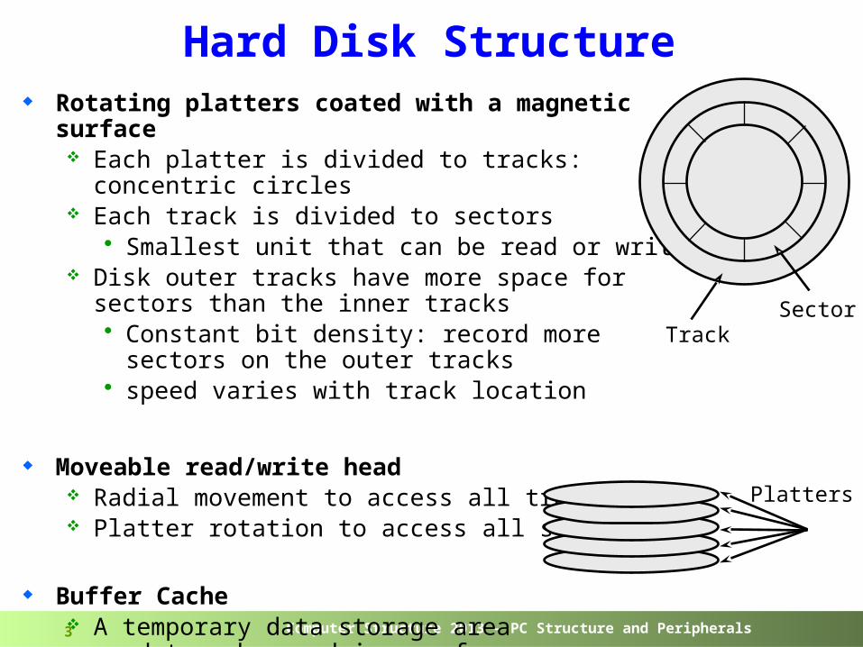
Hard Disk Structure Rotating platters coated with a magnetic surface
Each platter is divided to tracks: concentric circles Each track is divided to sectors
• Smallest unit that can be read or written Disk outer tracks have more space for
sectors than the inner tracks• Constant bit density: record more
sectors on the outer tracks• speed varies with track location
Moveable read/write head Radial movement to access all tracks Platter rotation to access all sectors
Buffer Cache A temporary data storage area
used to enhance drive performance
Platters
TrackSector
Computer Structure 2013 – PC Structure and Peripherals4
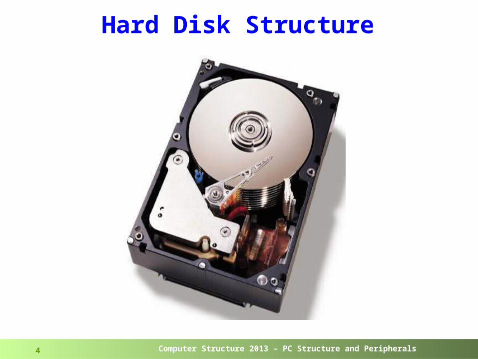
Hard Disk Structure
Computer Structure 2013 – PC Structure and Peripherals5
Disk Access Seek: position the head over the proper track
Average: Sum of the time for all possible seek / total # of possible seeks
Due to locality of disk reference, actual average seek is shorter: 4 to 12 ms
Rotational latency: wait for desired sector to rotate under head The faster the drives spins, the shorter the rotational latency time Most disks rotate at 5,400 to 15,000 RPM
• At 7200 RPM: 8 ms per revolution An average latency to the desired information is halfway around the
disk• At 7200 RPM: 4 ms
Transfer block: read/write the data Transfer time is a function of: sector size, rotation speed,
and recording density: bits per inch on a track Typical values: 100 MB / sec
Disk Access Time = Seek time + Rotational Latency + Transfer time + Controller Time + Queuing Delay
Computer Structure 2013 – PC Structure and Peripherals6
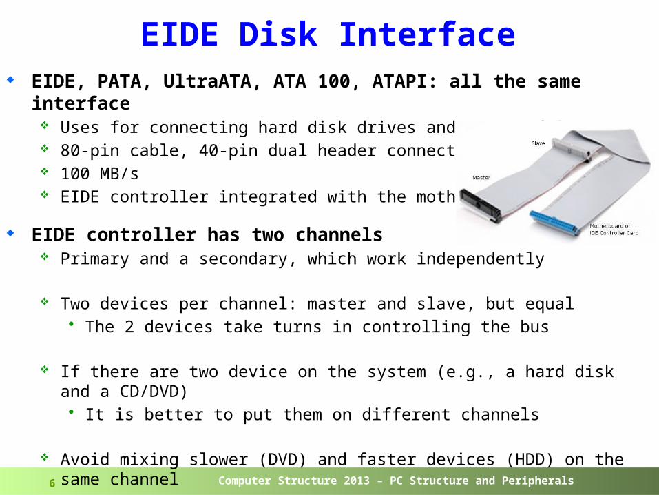
EIDE Disk Interface EIDE, PATA, UltraATA, ATA 100, ATAPI: all the same
interface Uses for connecting hard disk drives and CD/DVD drives 80-pin cable, 40-pin dual header connector 100 MB/s EIDE controller integrated with the motherboard
EIDE controller has two channels Primary and a secondary, which work independently
Two devices per channel: master and slave, but equal• The 2 devices take turns in controlling the bus
If there are two device on the system (e.g., a hard disk and a CD/DVD)• It is better to put them on different channels
Avoid mixing slower (DVD) and faster devices (HDD) on the same channel
If doing a lot of copying from drive to drive• Better performance by separating devices to separate channels
Computer Structure 2013 – PC Structure and Peripherals7
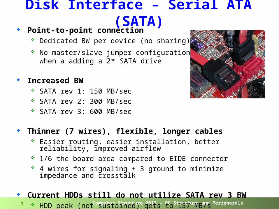
Disk Interface – Serial ATA (SATA) Point-to-point connection
Dedicated BW per device (no sharing) No master/slave jumper configuration needed
when a adding a 2nd SATA drive
Increased BW SATA rev 1: 150 MB/sec SATA rev 2: 300 MB/sec SATA rev 3: 600 MB/sec
Thinner (7 wires), flexible, longer cables Easier routing, easier installation, better reliability, improved
airflow 1/6 the board area compared to EIDE connector 4 wires for signaling + 3 ground to minimize impedance and
crosstalk
Current HDDs still do not utilize SATA rev 3 BW HDD peak (not sustained) gets to 157 MB/s SSD gets to 250 MB/sec
Computer Structure 2013 – PC Structure and Peripherals8
Flash Memory Flash is a non-volatile, rewritable memory
NOR Flash Supports per-byte data read and write (random access)
• Erasing (setting all the bits) done only at block granularity (64-128KB)
• Writing (clearing a bit) can be done at byte granularity Suitable for storing code (e.g. BIOS, cell phone firmware)
NAND Flash Supports page-mode read and write (0.5KB – 4KB per page)
• Erasing (setting all the bits) done only at block granularity (64-128KB)
Suitable for storing large data (e.g. pictures, songs)• Similar to other secondary data storage devices
Reduced erase and write times Greater storage density and lower cost per bit
Computer Structure 2013 – PC Structure and Peripherals9
Flash Memory Principles of Operation
Information is stored in an array of memory cells In single-level cell (SLC) devices, each cell stores one bit Multi-level cell (MLC) devices store multiple bits per cell using multiple
levels of electrical charge
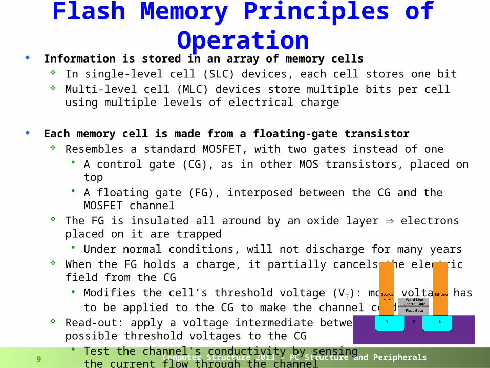
Each memory cell is made from a floating-gate transistor Resembles a standard MOSFET, with two gates instead of one
• A control gate (CG), as in other MOS transistors, placed on top• A floating gate (FG), interposed between the CG and the MOSFET
channel The FG is insulated all around by an oxide layer electrons placed on it
are trapped • Under normal conditions, will not discharge for many years
When the FG holds a charge, it partially cancels the electric field from the CG• Modifies the cell’s threshold voltage (VT): more voltage has to be
applied to the CG to make the channel conduct Read-out: apply a voltage intermediate between the
possible threshold voltages to the CG• Test the channel's conductivity by sensing
the current flow through the channel• In a MLC device, sense the amount of current flow
Computer Structure 2013 – PC Structure and Peripherals10
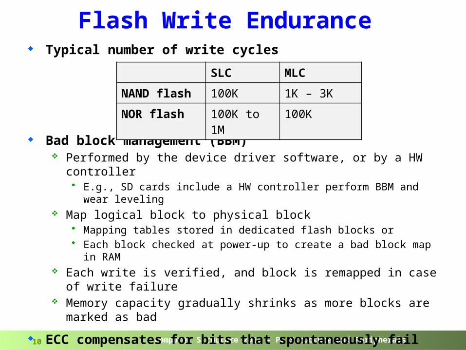
Flash Write Endurance Typical number of write cycles
Bad block management (BBM) Performed by the device driver software, or by a HW controller
• E.g., SD cards include a HW controller perform BBM and wear leveling
Map logical block to physical block • Mapping tables stored in dedicated flash blocks or • Each block checked at power-up to create a bad block map in RAM
Each write is verified, and block is remapped in case of write failure
Memory capacity gradually shrinks as more blocks are marked as bad
ECC compensates for bits that spontaneously fail 22 (24) bits of ECC code correct a one bit error in 2048 (4096)
data bits If ECC cannot correct the error during read, it may still detect
the error
SLC MLCNAND flash 100K 1K – 3K NOR flash 100K to
1M 100K
Computer Structure 2013 – PC Structure and Peripherals11
Flash Write Endurance (cont) Wear-leveling algorithms
Evenly distribute data across flash memory and move data around
Prevent from one portion to wear out faster than another SSD's controller keeps a record of where data is set down on the
drive as it is relocated from one portion to another
Dynamic wear leveling Map Logical Block Addresses (LBAs) to physical Flash memory
addresses Each time a block of data is written, it is written to a new
location• Link the new block • Mark original physical block as invalid data• Blocks that never get written remain in the same location
Static wear leveling Periodically move blocks which are not written Allow these low usage cells be used by other data
Computer Structure 2013 – PC Structure and Peripherals12
Solid State Drive – SSD Most manufacturers use "burst rate" for Performance
numbers Not its steady state or average read rate
Any write operation requires an erase followed by the write When SSD is new, NAND flash memory is pre-erased
Consumer-grade multi-level cell (MLC) Allows ≥2 bit per flash memory cell Sustains 2,000 to 10,000 write cycles Notably less expensive than SLC drives
Enterprise-class single-level cell (SLC) Allows 1 bit per flash memory cell Lasts 10× write cycles of an MLC
The more write/erase cycle the shorter the drive's lifespan Use wear-leveling algorithms to evenly distribute writes DRAM cache to buffer data writes to reduce number of
write/erase cycles Extra memory cells to be used when blocks of flash memory
wear out
Computer Structure 2013 – PC Structure and Peripherals13
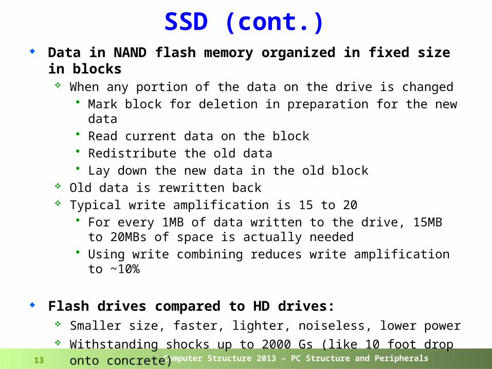
SSD (cont.) Data in NAND flash memory organized in fixed size in
blocks When any portion of the data on the drive is changed
• Mark block for deletion in preparation for the new data• Read current data on the block• Redistribute the old data• Lay down the new data in the old block
Old data is rewritten back Typical write amplification is 15 to 20
• For every 1MB of data written to the drive, 15MB to 20MBs of space is actually needed
• Using write combining reduces write amplification to ~10%
Flash drives compared to HD drives: Smaller size, faster, lighter, noiseless, lower power Withstanding shocks up to 2000 Gs (like 10 foot drop onto
concrete) More expensive (cost/byte): ~2$/1GB vs ~0.1$/1GB in HDD
Computer Structure 2013 – PC Structure and Peripherals14
The Motherboard
Computer Structure 2013 – PC Structure and Peripherals15
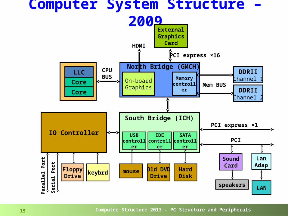
Computer System Structure – 2009
Core
PCI
North Bridge (GMCH)DDRII
Channel 1
mouse
LAN
LanAdap
External Graphics
Card
Mem BUS
LLC
SoundCard
speakers
South Bridge (ICH)
PCI express ×16
IDEcontroller
IO Controller
Old DVDDrive
HardDisk
Para
llel P
ort
Seria
l Por
t
FloppyDrive keybrd
DDRIIChannel 2
USBcontroller
SATAcontroller
PCI express ×1
Memory controller
On-board Graphics
CPU BUS
Core
HDMI
Computer Structure 2013 – PC Structure and Peripherals16
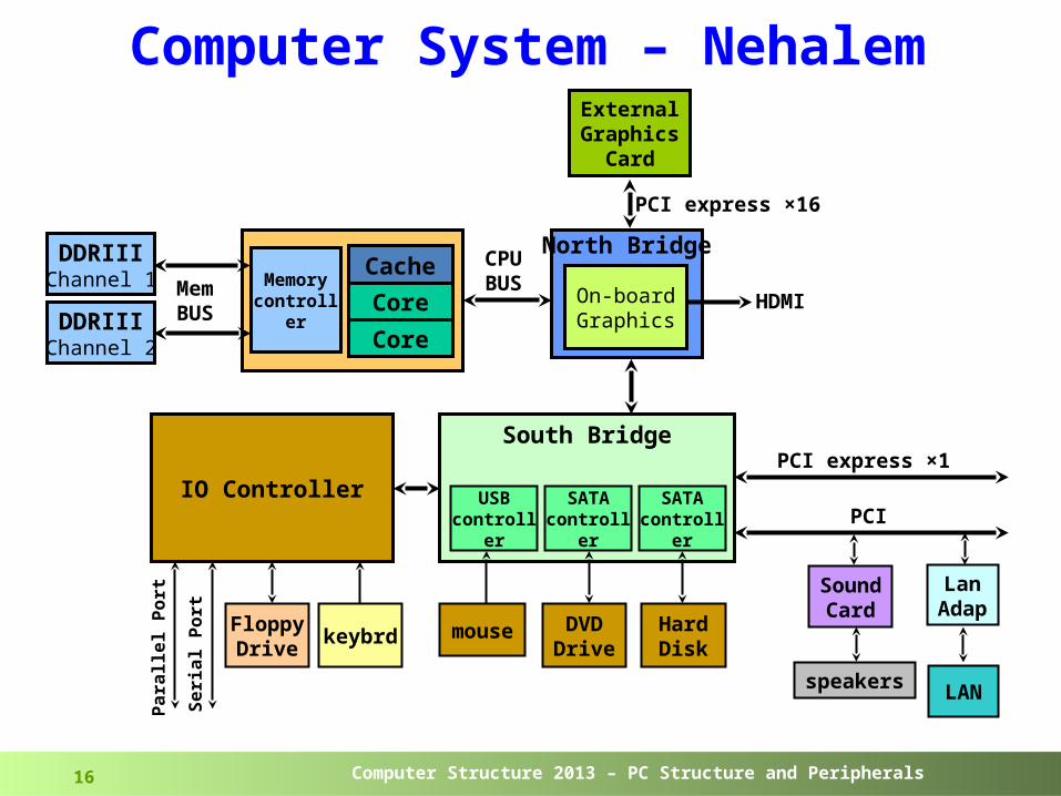
Computer System – Nehalem
PCI
North Bridge
mouse
LAN
LanAdap
External Graphics
Card
CPU BUS
SoundCard
speakers
South Bridge
PCI express ×16
SATAcontroller
IO Controller
DVDDrive
HardDisk
Para
llel P
ort
Seria
l Por
t
FloppyDrive keybrd
USBcontroller
SATAcontroller
PCI express ×1
On-board Graphics
CacheDDRIIIChannel 1 Mem
BUSDDRIIIChannel 2
Memory controller Core
CoreHDMI
Computer Structure 2013 – PC Structure and Peripherals17
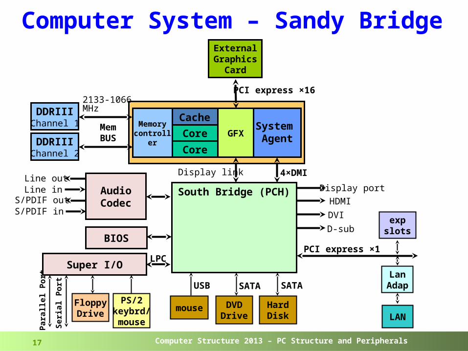
Computer System – Sandy Bridge
mouseLAN
LanAdap
South Bridge (PCH)Audio Codec
DVDDrive
HardDiskPa
ralle
l Por
t
Seria
l Por
t
FloppyDrive
PS/2keybrd/mouse
CacheDDRIIIChannel 1 Mem
BUSDDRIIIChannel 2
Memory controller Core
Core
Display port
External Graphics
Card
PCI express ×16
GFX
Display link
2133-1066 MHz
Line inLine out
S/PDIF inS/PDIF out
Super I/O LPC
USB SATA SATA
BIOSPCI express ×1
expslots
System Agent
4×DMI
D-sub
HDMIDVI
Computer Structure 2013 – PC Structure and Peripherals18
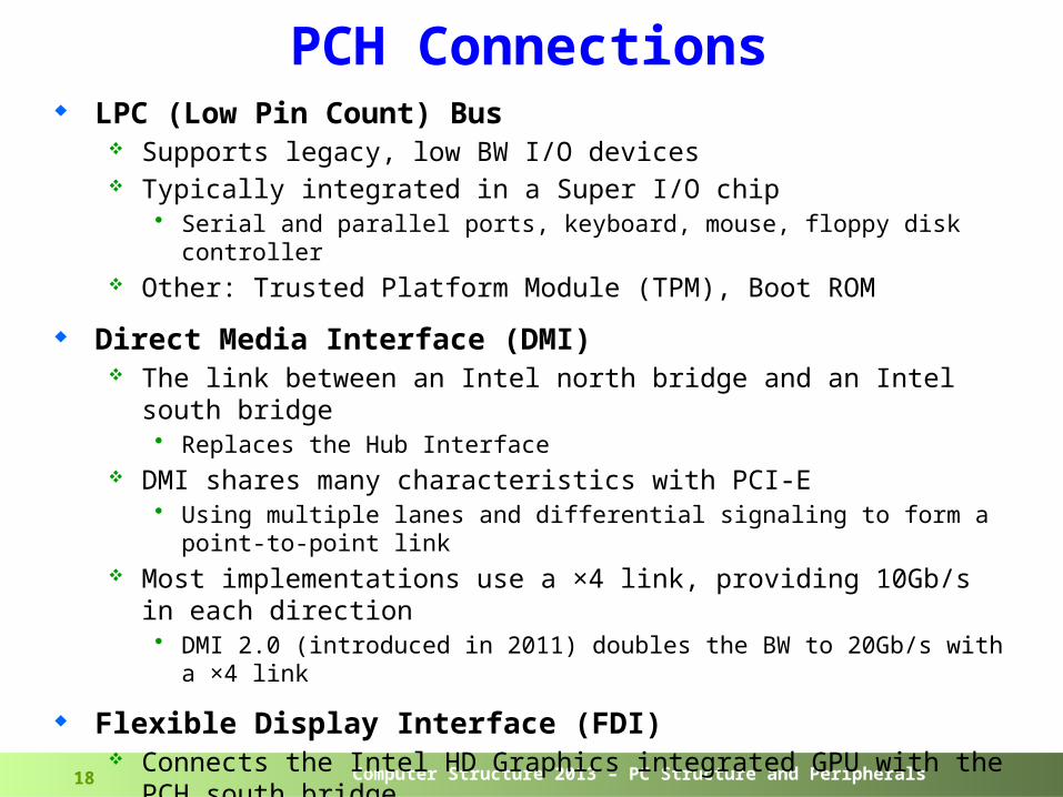
PCH Connections LPC (Low Pin Count) Bus
Supports legacy, low BW I/O devices Typically integrated in a Super I/O chip
• Serial and parallel ports, keyboard, mouse, floppy disk controller Other: Trusted Platform Module (TPM), Boot ROM
Direct Media Interface (DMI) The link between an Intel north bridge and an Intel south bridge
• Replaces the Hub Interface DMI shares many characteristics with PCI-E
• Using multiple lanes and differential signaling to form a point-to-point link
Most implementations use a ×4 link, providing 10Gb/s in each direction • DMI 2.0 (introduced in 2011) doubles the BW to 20Gb/s with a ×4 link
Flexible Display Interface (FDI) Connects the Intel HD Graphics integrated GPU with the PCH
south bridge• where display connectors are attached
Supports 2 independent 4-bit fixed frequency links/channels/pipes at 2.7GT/s data rate
Computer Structure 2013 – PC Structure and Peripherals19
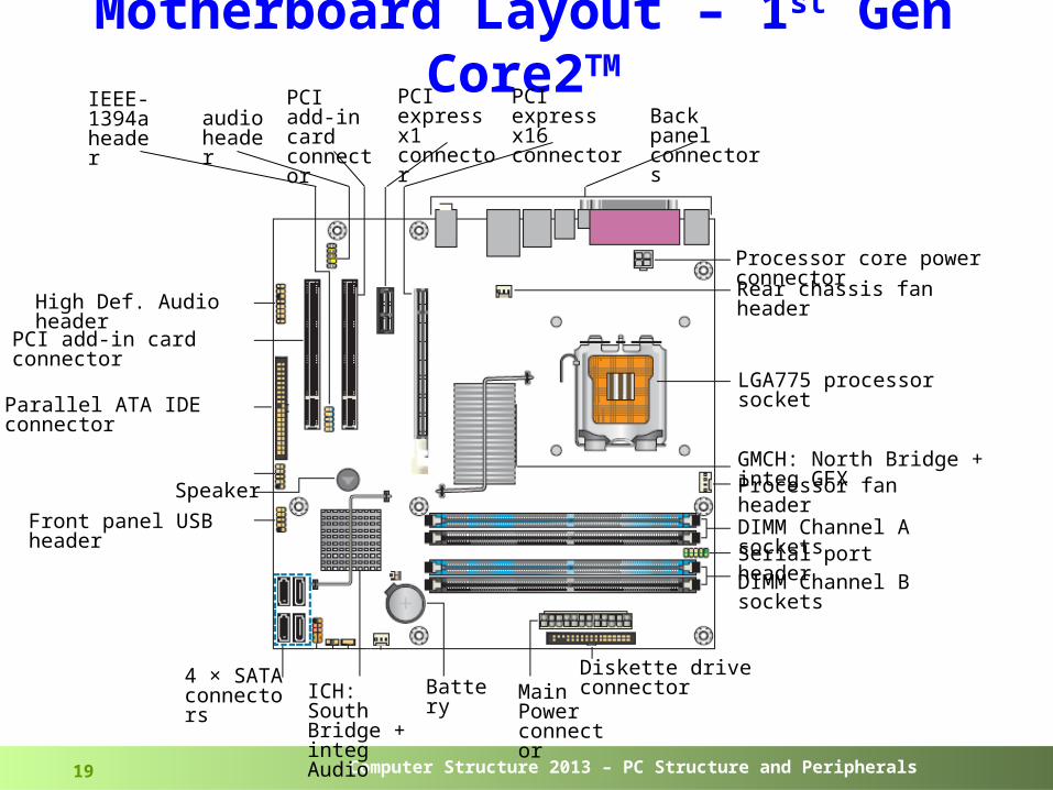
Motherboard Layout – 1st Gen Core2TM
IEEE-1394a header
audio header
PCI add-in card connector
PCI express x1 connector
PCI express x16 connector
Back panel connectors
Processor core power connectorRear chassis fan header
LGA775 processor socket
GMCH: North Bridge + integ GFXProcessor fan header
DIMM Channel A socketsSerial port headerDIMM Channel B sockets
Diskette drive connectorMain Power connector
BatteryICH: South Bridge + integ Audio
4 × SATA connectors
Front panel USB headerSpeaker
Parallel ATA IDE connector
High Def. Audio header
PCI add-in card connector
Computer Structure 2013 – PC Structure and Peripherals20
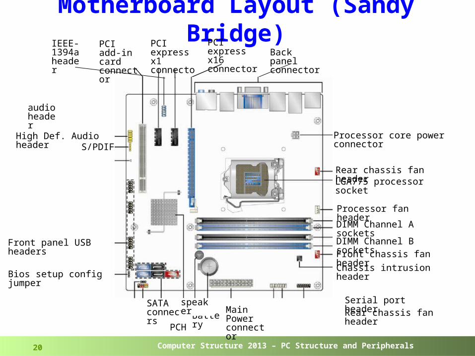
Motherboard Layout (Sandy Bridge)IEEE-
1394a header
audio header
PCI add-in card connector
PCI express x1 connector
PCI express x16 connector
Back panel connectors
Processor core power connector
Rear chassis fan header
LGA775 processor socket
Processor fan header
DIMM Channel A sockets
Serial port header
DIMM Channel B sockets
Main Power connector
BatteryPCH
SATA connectors
Front panel USB headers
Bios setup config jumper
High Def. Audio headerS/PDIF
speaker
Front chassis fan headerChassis intrusion header
Rear chassis fan header
Computer Structure 2013 – PC Structure and Peripherals21
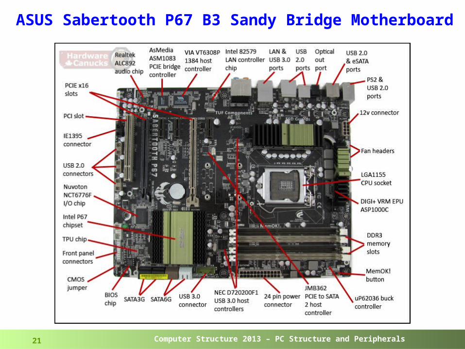
ASUS Sabertooth P67 B3 Sandy Bridge Motherboard
Computer Structure 2013 – PC Structure and Peripherals22
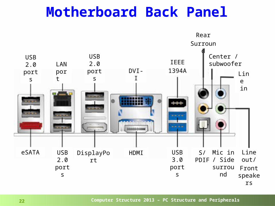
Motherboard Back Panel
USB 2.0 port
s
LANport
USB 2.0 port
s
USB 3.0 port
s
eSATA USB 2.0 port
s
DisplayPort
HDMI
DVI-IIEEE1394
A
RearSurroun
d
Line in
Line out/Front
speakers
S/PDIF
Center /subwoofer
Mic in/ Side
surround
Computer Structure 2013 – PC Structure and Peripherals23
System Start-upUpon computer turn-on several events occur:
1. The CPU "wakes up" and sends a message to activate the BIOS
2. BIOS runs the Power On Self Test (POST): make sure system devices are working ok Initialize system hardware and chipset registers Initialize power management Test RAM Enable the keyboard Test serial and parallel ports Initialize floppy disk drives and hard disk drive controllers Displays system summary information
Computer Structure 2013 – PC Structure and Peripherals24
System Start-up (cont.)3. During POST, the BIOS compares the system configuration
data obtained from POST with the system information stored on a memory chip located on the MB
A CMOS chip, which is updated whenever new system components are added
Contains the latest information about system components
4. After the POST tasks are completed the BIOS looks for the boot program responsible for loading
the operating system Usually, the BIOS looks on the floppy disk drive A: followed
by drive C:
5. After boot program is loaded into memory It loads the system configuration information contained in
the registry in a Windows® environment, and device drivers
6. Finally, the operating system is loaded
Computer Structure 2013 – PC Structure and Peripherals25
Backup
Computer Structure 2013 – PC Structure and Peripherals26
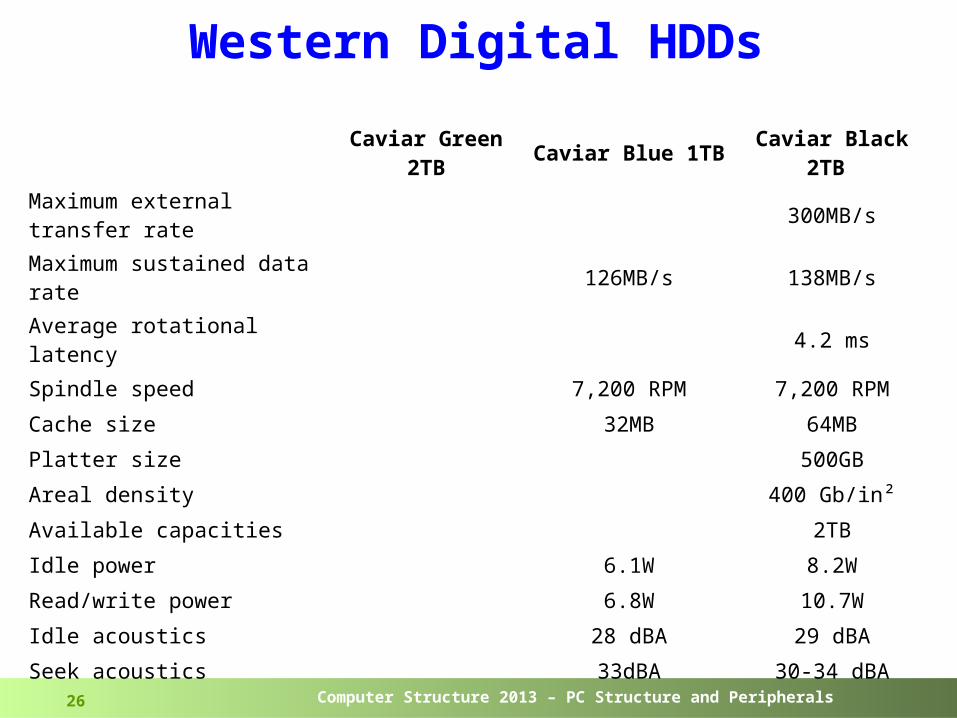
Western Digital HDDsCaviar Green
2TB Caviar Blue 1TB Caviar Black 2TB
Maximum external transfer rate 300MB/sMaximum sustained data rate 126MB/s 138MB/sAverage rotational latency 4.2 msSpindle speed 7,200 RPM 7,200 RPMCache size 32MB 64MBPlatter size 500GBAreal density 400 Gb/in²Available capacities 2TBIdle power 6.1W 8.2WRead/write power 6.8W 10.7WIdle acoustics 28 dBA 29 dBASeek acoustics 33dBA 30-34 dBA
Computer Structure 2013 – PC Structure and Peripherals27
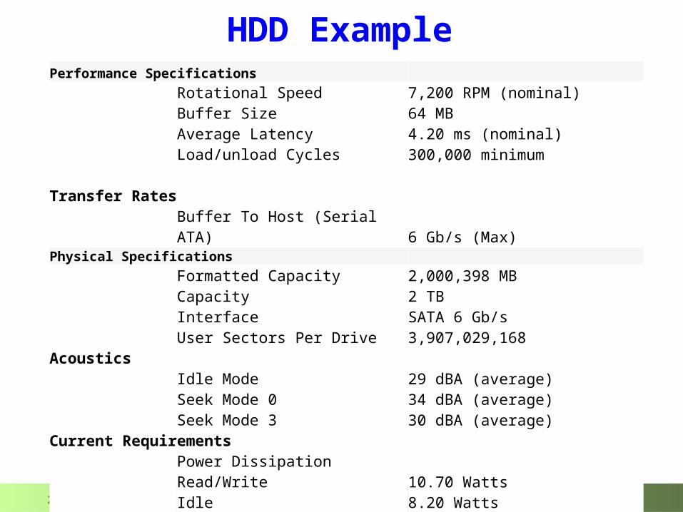
HDD ExamplePerformance Specifications Rotational Speed 7,200 RPM (nominal) Buffer Size 64 MB Average Latency 4.20 ms (nominal) Load/unload Cycles 300,000 minimum Transfer Rates Buffer To Host (Serial ATA) 6 Gb/s (Max)Physical Specifications Formatted Capacity 2,000,398 MB Capacity 2 TB Interface SATA 6 Gb/s User Sectors Per Drive 3,907,029,168Acoustics Idle Mode 29 dBA (average) Seek Mode 0 34 dBA (average) Seek Mode 3 30 dBA (average)Current Requirements Power Dissipation Read/Write 10.70 Watts Idle 8.20 Watts Standby 1.30 Watts Sleep 1.30 Watts
Computer Structure 2013 – PC Structure and Peripherals28
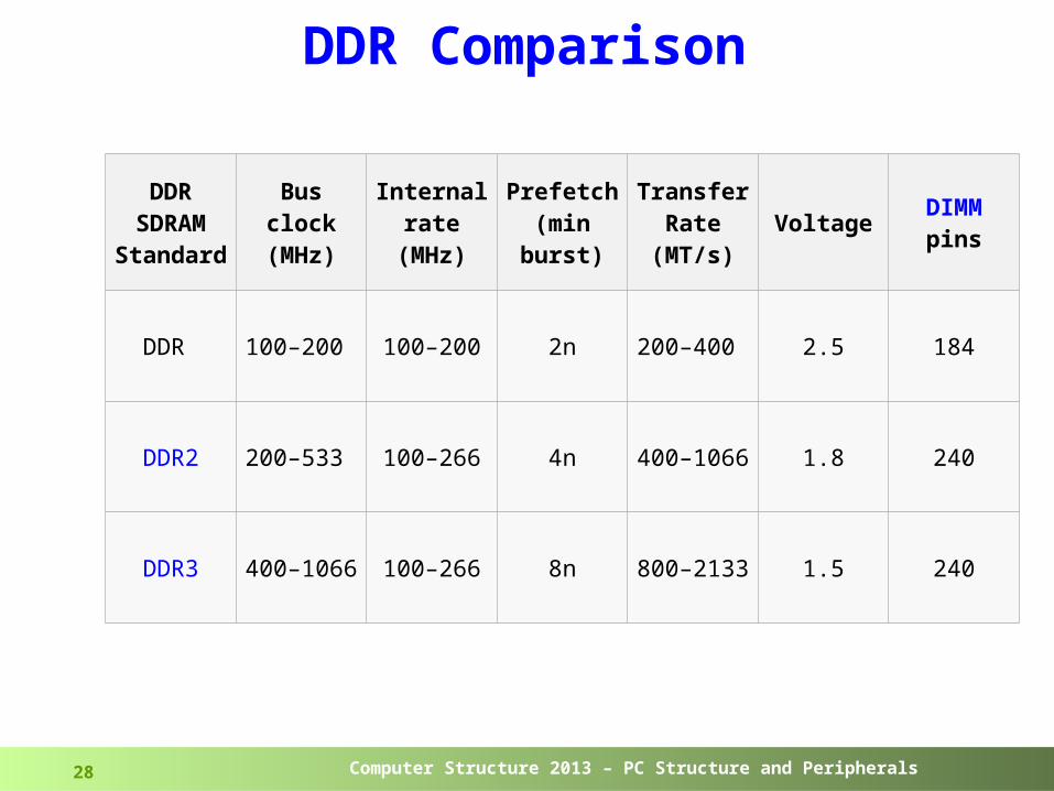
DDR Comparison
DDR SDRAMStandar
d
Bus clock(MHz)
Internal rate
(MHz)
Prefetch(min
burst)
Transfer Rate
(MT/s)Voltage DIMM
pins
DDR 100–200 100–200 2n 200–
400 2.5 184
DDR2 200–533 100–266 4n 400–
1066 1.8 240
DDR3 400–1066 100–266 8n 800–
2133 1.5 240
Computer Structure 2013 – PC Structure and Peripherals29
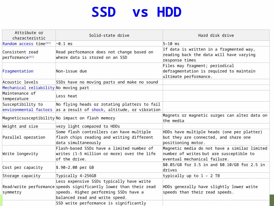
SSD vs HDDAttribute or characteristic Solid-state drive Hard disk driveRandom access time[57] ~0.1 ms 5–10 msConsistent read performance[61]
Read performance does not change based on where data is stored on an SSD
If data is written in a fragmented way, reading back the data will have varying response times
Fragmentation Non-issue due Files may fragment; periodical defragmentation is required to maintain ultimate performance.
Acoustic levels SSDs have no moving parts and make no soundMechanical reliability No moving partMaintenance of temperature Less heatSusceptibility to environmental factors
No flying heads or rotating platters to fail as a result of shock, altitude, or vibration
Magneticsusceptibility No impact on flash memory Magnets or magnetic surges can alter data on the media
Weight and size very light compared to HDDsParallel operation Some flash controllers can have multiple flash chips
reading and writing different data simultaneouslyHDDs have multiple heads (one per platter) but they are connected, and share one positioning motor.
Write longevity Flash-based SSDs have a limited number of writes (1-5 million or more) over the life of the drive.
Magnetic media do not have a similar limited number of writes but are susceptible to eventual mechanical failure.
Cost per capacity $.90–2.00 per GB $0.05/GB for 3.5 in and $0.10/GB for 2.5 in drivesStorage capacity Typically 4-256GB typically up to 1 – 2 TB
Read/write performance symmetry
Less expensive SSDs typically have write speeds significantly lower than their read speeds. Higher performing SSDs have a balanced read and write speed.
HDDs generally have slightly lower write speeds than their read speeds.
Free block availability and TRIM
SSD write performance is significantly impacted by the availability of free, programmable blocks. Previously written data blocks that are no longer in use can be reclaimed by TRIM; however, even with TRIM, fewer free, programmable blocks translates into reduced performance.[29][75][76]
HDDs are not affected by free blocks or the operation (or lack) of the TRIM command
Power consumption High performance flash-based SSDs generally require 1/2 to 1/3 the power of HDDs
High performance HDDs require 12-18 watts; drives designed for notebook computers are typically 2 watts.
Computer Structure 2013 – PC Structure and Peripherals30
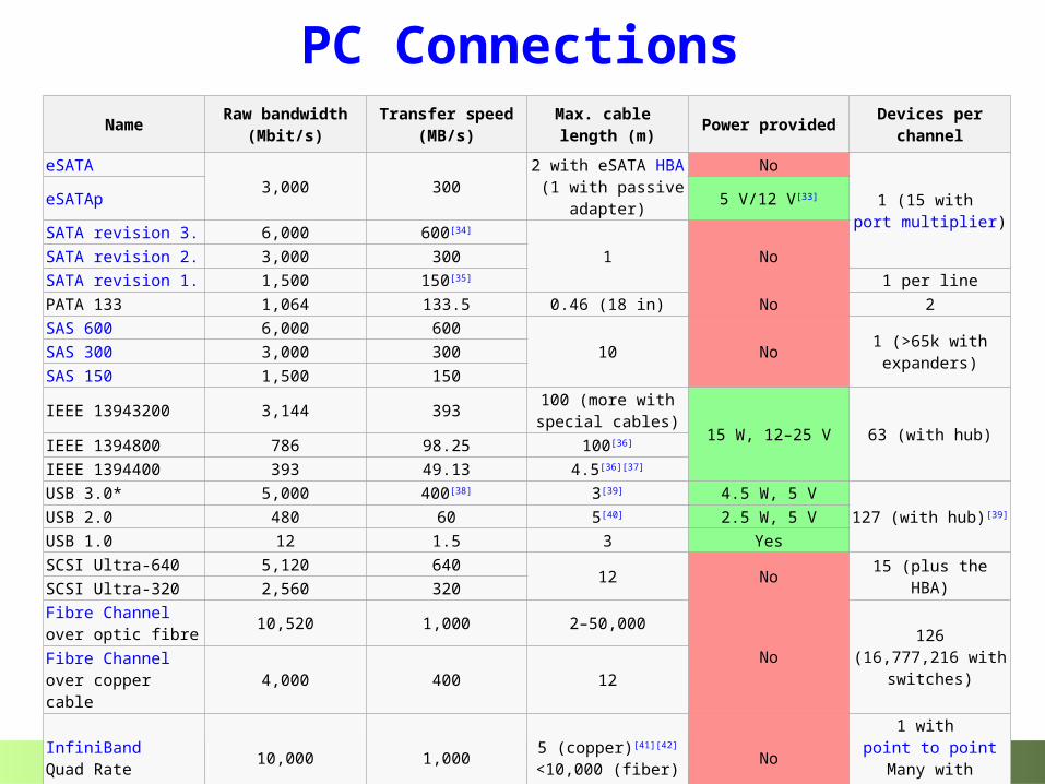
PC ConnectionsName Raw bandwidth
(Mbit/s)Transfer speed
(MB/s)Max. cable length (m) Power provided Devices per
channeleSATA
3,000 3002 with eSATA HBA (1 with passive
adapter)
No1 (15 with
port multiplier)eSATAp 5 V/12 V[33]
SATA revision 3.0 6,000 600[34]
1 NoSATA revision 2.0 3,000 300SATA revision 1.0 1,500 150[35] 1 per linePATA 133 1,064 133.5 0.46 (18 in) No 2SAS 600 6,000 600
10 No 1 (>65k with expanders)SAS 300 3,000 300
SAS 150 1,500 150IEEE 13943200 3,144 393 100 (more with
special cables) 15 W, 12–25 V 63 (with hub)IEEE 1394800 786 98.25 100[36]
IEEE 1394400 393 49.13 4.5[36][37]
USB 3.0* 5,000 400[38] 3[39] 4.5 W, 5 V127 (with hub)[39]USB 2.0 480 60 5[40] 2.5 W, 5 V
USB 1.0 12 1.5 3 YesSCSI Ultra-640 5,120 640 12 No 15 (plus the HBA)SCSI Ultra-320 2,560 320Fibre Channelover optic fibre 10,520 1,000 2–50,000
No126
(16,777,216 with switches)Fibre Channel
over copper cable 4,000 400 12
InfiniBandQuad Rate 10,000 1,000 5 (copper)[41][42]
<10,000 (fiber) No1 with
point to pointMany with
switched fabricThunderbolt 10,000 1,250 100 10 W 7
Computer Structure 2013 – PC Structure and Peripherals31
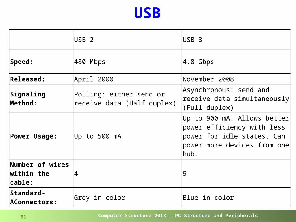
USBUSB 2 USB 3
Speed: 480 Mbps 4.8 Gbps
Released: April 2000 November 2008Signaling Method:
Polling: either send or receive data (Half duplex)
Asynchronous: send and receive data simultaneously (Full duplex)
Power Usage: Up to 500 mAUp to 900 mA. Allows better power efficiency with less power for idle states. Can power more devices from one hub.
Number of wires within the cable:
4 9
Standard-AConnectors: Grey in color Blue in color