configuring embeddable adaptive computing systems … · 2011-05-13 · configuring embeddable...
TRANSCRIPT
AFRL-IF-RS-TR-2003-212 Final Technical Report September 2003 CONFIGURING EMBEDDABLE ADAPTIVE COMPUTING SYSTEMS FOR MULTIPLE APPLICATION DOMAINS WITH MINIMAL SIZE, WEIGHT, AND POWER Texas Tech University Sponsored by Defense Advanced Research Projects Agency DARPA Order No. F297, J468
APPROVED FOR PUBLIC RELEASE; DISTRIBUTION UNLIMITED.
The views and conclusions contained in this document are those of the authors and should not be interpreted as necessarily representing the official policies, either expressed or implied, of the Defense Advanced Research Projects Agency or the U.S. Government.
AIR FORCE RESEARCH LABORATORY INFORMATION DIRECTORATE
ROME RESEARCH SITE ROME, NEW YORK
This report has been reviewed by the Air Force Research Laboratory, Information Directorate, Public Affairs Office (IFOIPA) and is releasable to the National Technical Information Service (NTIS). At NTIS it will be releasable to the general public, including foreign nations. AFRL-IF-RS-TR-2003-212 has been reviewed and is approved for publication.
APPROVED: /s/ JULES BERGMANN Project Engineer
FOR THE DIRECTOR: /s/ EUGENE C. BLACKBURN, Chief Information Technology Division Information Directorate
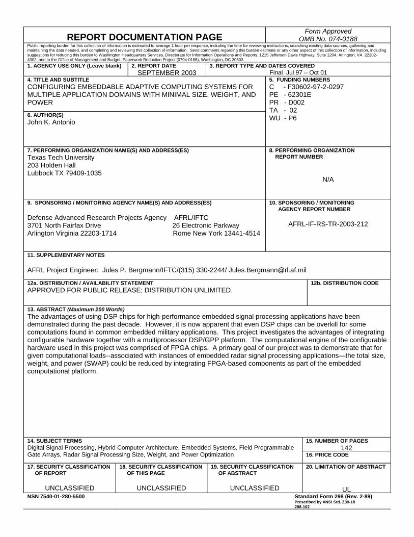
REPORT DOCUMENTATION PAGE Form Approved
OMB No. 074-0188 Public reporting burden for this collection of information is estimated to average 1 hour per response, including the time for reviewing instructions, searching existing data sources, gathering and maintaining the data needed, and completing and reviewing this collection of information. Send comments regarding this burden estimate or any other aspect of this collection of information, including suggestions for reducing this burden to Washington Headquarters Services, Directorate for Information Operations and Reports, 1215 Jefferson Davis Highway, Suite 1204, Arlington, VA 22202-4302, and to the Office of Management and Budget, Paperwork Reduction Project (0704-0188), Washington, DC 20503 1. AGENCY USE ONLY (Leave blank)
2. REPORT DATESEPTEMBER 2003
3. REPORT TYPE AND DATES COVERED Final Jul 97 – Oct 01
4. TITLE AND SUBTITLE CONFIGURING EMBEDDABLE ADAPTIVE COMPUTING SYSTEMS FOR MULTIPLE APPLICATION DOMAINS WITH MINIMAL SIZE, WEIGHT, AND POWER
6. AUTHOR(S) John K. Antonio
5. FUNDING NUMBERS C - F30602-97-2-0297 PE - 62301E PR - D002 TA - 02 WU - P6
7. PERFORMING ORGANIZATION NAME(S) AND ADDRESS(ES) Texas Tech University 203 Holden Hall Lubbock TX 79409-1035
8. PERFORMING ORGANIZATION REPORT NUMBER
N/A
9. SPONSORING / MONITORING AGENCY NAME(S) AND ADDRESS(ES) Defense Advanced Research Projects Agency AFRL/IFTC 3701 North Fairfax Drive 26 Electronic Parkway Arlington Virginia 22203-1714 Rome New York 13441-4514
10. SPONSORING / MONITORING AGENCY REPORT NUMBER
AFRL-IF-RS-TR-2003-212
11. SUPPLEMENTARY NOTES AFRL Project Engineer: Jules P. Bergmann/IFTC/(315) 330-2244/ [email protected]
12a. DISTRIBUTION / AVAILABILITY STATEMENT APPROVED FOR PUBLIC RELEASE; DISTRIBUTION UNLIMITED.
12b. DISTRIBUTION CODE
13. ABSTRACT (Maximum 200 Words) The advantages of using DSP chips for high-performance embedded signal processing applications have been demonstrated during the past decade. However, it is now apparent that even DSP chips can be overkill for some computations found in common embedded military applications. This project investigates the advantages of integrating configurable hardware together with a multiprocessor DSP/GPP platform. The computational engine of the configurable hardware used in this project was comprised of FPGA chips. A primary goal of our project was to demonstrate that for given computational loads--associated with instances of embedded radar signal processing applications—the total size, weight, and power (SWAP) could be reduced by integrating FPGA-based components as part of the embedded computational platform.
15. NUMBER OF PAGES142
14. SUBJECT TERMS Digital Signal Processing, Hybrid Computer Architecture, Embedded Systems, Field Programmable Gate Arrays, Radar Signal Processing Size, Weight, and Power Optimization 16. PRICE CODE
17. SECURITY CLASSIFICATION OF REPORT
UNCLASSIFIED
18. SECURITY CLASSIFICATION OF THIS PAGE
UNCLASSIFIED
19. SECURITY CLASSIFICATION OF ABSTRACT
UNCLASSIFIED
20. LIMITATION OF ABSTRACT
ULNSN 7540-01-280-5500 Standard Form 298 (Rev. 2-89)
Prescribed by ANSI Std. Z39-18 298-102
i
Table of Contents
Introduction .................................................................................................................................................... 1 Organizational Structure of the Report ...................................................................................................... 1 Project Overview ........................................................................................................................................ 2 Brief Descriptions of Major Parts of the Report ........................................................................................ 3
Part 1: Optimal Multiprocessor Configuration for SAR ................................................................................ 5 Overview of References [1A], [2B], and [3].............................................................................................. 5
Part 2: Optimal Communication Scheduling for STAP ................................................................................. 9 Overview of References [4C], [5D], [6E], [7], and [8] ............................................................................ 9
Part 3: FPGA Power Prediction and Applications ....................................................................................... 12 3.1 FPGA Power Prediction ..................................................................................................................... 12 Overview of References [9F] and [10] .................................................................................................... 12 Overview of Reference [11G]................................................................................................................... 14 3.2 FPGA Applications ............................................................................................................................ 14 Overview of References [12H] and [13] .................................................................................................. 14 Overview of Reference [14] ..................................................................................................................... 15 Overview of Reference [15I] .................................................................................................................... 16 Overview of References [16J] and [17] ................................................................................................... 18
Part 4: Hybrid FPGA/DSP/GPP Platform .................................................................................................... 19 Overview of Reference [18K] ................................................................................................................... 19
Conclusion.................................................................................................................................................... 33 Technology Transfer................................................................................................................................. 33 Deliverables.............................................................................................................................................. 33
References .................................................................................................................................................... 35 Additional Materials..................................................................................................................................... 38 Technical Report .......................................................................................................................................... 38 Appendix A: Jeffrey T. Muehring and John K. Antonio, “Optimal Configuration of an Embedded Parallel System for Synthetic Aperture Radar Processing,” Proceedings of the International Conference on Signal Processing Applications & Technology, Boston, MA, Oct. 1996, pp. 1489-1494....................................... 40 Appendix B: Jeffrey T. Muehring and John K. Antonio, “Optimal Configuration of Compute Nodes for Synthetic Aperture Radar Processing,” Proceedings of the International Workshop on Embedded HPC Systems and Applications (EHPC ‘98), in Lecture Notes in Computer Science 1388: Parallel and Distributed Processing, edited by Jose Rolim, sponsor: IEEE Computer Society, Orlando, FL, USA, Apr. 1998, pp. 987-993. ....................................................................................................................................... 47 Appendix C: Jack M. West and John K. Antonio, “Simulation of the Communication Time for a Space-Time Adaptive Processing Algorithm on a Parallel Embedded System,” Proceedings of the International Workshop on Embedded HPC Systems and Applications (EHPC ‘98), in Lecture Notes in Computer Science 1388: Parallel and Distributed Processing, edited by Jose Rolim, sponsor: IEEE Computer Society, Orlando, FL, USA, Apr. 1998, pp. 979-986................................................................................... 55 Appendix D: Jack M. West and John K. Antonio, “A Genetic Algorithm Approach to Scheduling Communications for a Class of Parallel Space-Time Adaptive Processing Algorithms,” Proceedings of the 5th International Workshop on Embedded/Distributed HPC Systems and Applications (EHPC 2000), in Lecture Notes in Computer Science, IPDPS 2000 Workshops, sponsor: IEEE Computer Society, Cancun, Mexico, May 2000, pp. 855-861. ................................................................................................................. 64 Appendix E: Jack M. West and John K. Antonio, “A Genetic-Algorithm Approach to Scheduling Communications for Embedded Parallel Space-Time Adaptive Processing Algorithms,” Journal of Parallel and Distributed Computing, Vol. 62, No. 9, Sept. 2002, pp. 1386-1406..................................................... 72 Appendix F: Timothy Osmulski, Jeffrey T. Muehring, Brian Veale, Jack M. West, Hongping Li, Sirirut Vanichayobon, Seok-Hyun Ko, John K. Antonio, and Sudarshan K. Dhall, “A Probabilistic Power Prediction Tool for the Xilinx 4000-Series FPGA,” Proceedings of the 5th International Workshop on
ii
Embedded/Distributed HPC Systems and Applications (EHPC 2000), in Lecture Notes in Computer Science, IPDPS 2000 Workshops, sponsor: IEEE Computer Society, Cancun, Mexico, May 2000, pp. 776-783................................................................................................................................................................ 94 Appendix G: Hongping Li, John K. Antonio, and Sudarshan K. Dhall, “Fast and Precise Power Prediction for Combinational Circuits,” Proceedings of the IEEE Symposium on VLSI, sponsor: IEEE, Tampa, FL, Feb 2003, pp. 254-259. .............................................................................................................................. 103 Appendix H: Nikhil D. Gupta, John K. Antonio, and Jack M. West, “Reconfigurable Computing for Space-Time Adaptive Processing” Proceedings of the Sixth Annual IEEE Symposium on Field Programmable Custom Computing Machines (FCCM), Napa, CA, USA, Apr. 1998, pp. 335-336. ................................. 110 Appendix I: Jeffrey T. Muehring and John K. Antonio, “Minimizing Power Consumption using Signal Activity Transformations for Very Deep FPGA Pipelines,” Proceedings of the Military and Aerospace Applications for Programmable Devices and Technologies Conference (MAPLD 2000), sponsors: NASA and Johns Hopkins University/Applied Physics Laboratory, Laurel, MD, Sep. 2000. .............................. 113 Appendix J: S. Vanichayobon, Sudarshan K. Dhall, S. Lakshmivarahan, and John K. Antonio, “Power-speed Trade-off in Parallel Prefix Circuits,” Proceedings of ITComm 2002, High-Performance Pervasive Computing Conference, sponsor: SPIE, Boston, MA, July/Aug. 2002, pp. 109-120. ............................... 117 Appendix K: Jack M. West, Hongping Li, Sirirut Vanichayobon, Jeffrey T. Muehring, John K. Antonio, and Sudarshan K. Dhall, “A Hybrid FPGA/DSP/GPP Prototype Architecture for SAR and STAP,” Proceedings of the Fourth Annual High Performance Embedded Computing Workshop, sponsors: U.S. Navy and Defense Advanced Research Projects Agency (DARPA), MIT Lincoln Laboratory Publications, Group 18, Lexington, MA, Sep. 2000, pp. 29-30. ..................................................................................... 130
iii
List of Figures
Figure 1. Organizational structure of the report. ................................................................ 1 Figure 2. This diagram illustrates the method of performing sectioned fast convolutions
on azimuth input data with a pre-stored kernel. Given that the kernel size is fixed, then if the section size is made large, a relatively small fraction of samples are discarded for each section, thus making processor efficiency high. Conversely, if the section size is small, then a relatively large fraction of samples must be discarded for each section, resulting in poor processor efficiency, but relatively small memory requirements. ................................................................................................................ 6
Figure 3. Optimal CN Configurations of the CN-constrained Model [2B]. ....................... 8 Figure 4. Measured power consumption of the configuration files and data sets from [9F].
.................................................................................................................................... 14 Figure 5. Structure of the deep pipeline............................................................................ 17 Figure 6. Using activity transformations to minimize power consumption. .................... 18 Figure 7. Block diagram of the FPGA/DSP/GPP prototype architecture........................ 20 Figure 8. Detail of the FPGA/DSP/GPP prototype architecture....................................... 21 Figure 9. Photograph of the FPGA/DSP/GPP prototype architecture. ............................. 22 Figure 10. Interface Design: Communication from Annapolis FPGA (F) to Mercury. ... 23 Figure 11. Interface Design: Communication from Mercury to Annapolis FPGA (B). ... 24 Figure 12. Illustration of how the major computational components of SAR processing
can be mapped onto the hybrid system. ..................................................................... 24 Figure 13. Illustration of how the major computational components of STAP processing
can be mapped onto the hybrid system. ..................................................................... 25 Figure 14. Figure 14. SAR Processing Flow. ................................................................... 25 Figure 15. Data distribution for Parallel SAR Processing on Mercury. ........................... 26 Figure 16. Space-time diagram for streaming parallel SAR processing........................... 27 Figure 17. Throughput requirements achieved for streaming parallel SAR processing... 28 Figure 18. Streaming parallel RT_STAP on Mercury Subsystem.................................... 29 Figure 19. Parallel RT_STAP on Mercury Subsystem..................................................... 30 Figure 20. Space-time diagram for parallel RT_STAP. ................................................... 31 Figure 21. Throughput requirements achieved for the medium case parallel RT_STAP. 32
iv
Acknowledgments
I would first like to acknowledge and thank the graduate students that worked on this project. Every publication associated with the project was co-authored with one or more graduate assistants and was based on research conducted in conjunction with a PhD dissertation or MS thesis.
Jeff Muehring (initially an MS student and later a PhD student) conducted research in the area of determining optimal configurations for SAR (synthetic aperture radar) processing. His work included the application of mathematical programming techniques for determining optimal multiprocessor configurations for SAR. His techniques centered on the concept of making the proper trade-off between processing hardware and memory so as to minimize the overall power consumption of the system, while satisfying throughput requirements. Jeff also made contributions in the domain of FPGA (field programmable gate array) design by proposing a new way of implementing two-dimensional signal processing tasks (including SAR) using very deep FPGA pipelines. In addition, Jeff played an important role in designing and implementing the hardware portions of the custom interfaces between the FPGA and DSP/GPP subsystems of the constructed prototype platform.
Jack West (initially an MS student and later a PhD student) conducted research in the area of minimizing communication time for STAP (space-time adaptive processing) executing on a multiprocessor. By minimizing communication overhead, he demonstrated that less hardware is required for given instances of STAP, thereby reducing SWAP (size, weight, and power). The first phase of Jack’s work included the development of a simulator for Mercury’s RACEway® interconnection network. This fast and efficient simulator was used in the second phase of his work in which genetic algorithm approaches were developed for solving the communication scheduling problem. Jack also played important roles in developing the prototype system by helping with the STAP application software implementation and by designing and implementing the software portions of the custom interfaces connecting the FPGA and DSP/GPP subsystems.
Tim Osmulski (MS student) developed and implemented an analytical tool, in software, for estimating power consumption of a configured FPGA chip. This tool, which was the first of its kind, demonstrated that it is indeed possible to accurately predict FPGA power consumption by applying existing analytical approaches. The accuracy of Tim’s tool was verified by comparing its predicted values with actual measured power consumption taken from an instrumented FPGA board.
Hongping Li (PhD student) developed a new analytical approach for estimating power consumption of circuits, including those implemented on a FPGA. His approach is based on a Markov chain signal model, and directly accounts for correlations present among the internal signals of the circuit. Hongping verified the accuracy of his approach using PSpice® based simulation studies. Hongping also lead the effort in implementing the parallel SAR application software on the multiprocessor system.
Nikhil Gupta (MS student) developed FPGA circuit designs to support core calculations required by STAP. His work demonstrated that 16-bit block floating point
v
arithmetic provides acceptable accuracy for many situations. The advantage of using block floating point arithmetic, instead of standard floating point, is the significant reduction in the size and power consumption of the corresponding circuits. His research illustrated that if the values of the input data are approximately uniformly distributed, then the block floating point approach delivers acceptable accuracy.
Brian Veale (initially an MS student and later a PhD student) conducted a study comparing different FPGA designs and implementations for an inner product co-processor. He studied two architectural approaches for the co-processor and two different types of arithmetic (integer and floating point) for a total of four combinations. For each implementation, he also studied the effect that employing different degrees of pipelining had on each design in terms of size, speed, and power consumption. His study of pipelining resulted in some counterintuitive results. In particular, while it is well known that increasing the degree of pipelining generally enables custom designs to be run at faster clock rates, the same is not always true for FPGA designs.
Sirirut Vanichayobon (PhD student) studied the power-speed trade-off for a class of circuits known as prefix circuits. These circuits are important in their own right, and are representative of the type of circuit often required in high-performance embedded applications. Through extensive analysis of a number of known prefix circuits, her work illustrates that the trade-off between power and speed is not always obvious to the circuit designer. Based on discoveries made through her research, some important guidelines for properly matching circuit characteristics with power and speed requirements are provided. Sirirut also lead the effort in implementing the parallel STAP application software on the multiprocessor system.
I would also like to acknowledge the work and contributions of faculty colleagues. Dr. Sudarshan Dhall served as co-PI on this project since the Fall of 1999; the time at which I became Director of Computer Science at the University of Oklahoma. Dr. Dhall made contributions in nearly all aspects of the project, and was particularly instrumental in guiding the research of graduate assistants Sirirut Vanichayobon and Hongping Li. Dr. Dhall’s expertise in system modeling – and probabilistic techniques in particular – was extremely valuable. The project also benefited greatly by the contributions of Dr. S. Lakshmivarahan. It was Dr. Lakshmivarahan that originally proposed the topic of Sirirut’s research, and he and Dr. Dhall served as co-advisors of her PhD committee.
Next, I would like to acknowledge the assistance and guidance of key defense personnel, starting with Rick Metzger of Rome Laboratory. Rick served as program manager for a related prior project I performed for Rome Laboratory, and it was this past work experience that enabled me to be successful in proposing and completing the present project for DARPA.
I would like to acknowledge the support and encouragement of José Muñoz, who served as the original program manager for DARPA’s ACS (Adaptive Computing Systems) program. José provided valuable feedback and perspective throughout the contract period. I had the opportunity to meet with José and his staff frequently, including at annual reviews, PI meetings, and other professional conferences. He actively encouraged and facilitated interaction and collaboration among the PIs of different

vi
projects, which ensured that the ACS program was cohesive and integrated. The interactions with other PIs was stimulating, and served to accelerate and improve the quality and relevance of the results delivered by all project PIs.
Assisting José Muñoz with the management of this project was Ralph Kohler of Rome Laboratory. I met with Ralph on a regular basis at meetings and conferences and communicated with him frequently through e-mail and telephone correspondence. Ralph made a number of technical contributions and refinements to the project, and often served as a sounding board on behalf of the military. He related to me the actual needs of the war fighter, and these insights helped us to provide results that were more applicable than would have otherwise been possible. Ralph also helped me tremendously with the overall management and organization of the project.
Finally, I would like to thank Jules Bergmann of Rome Laboratory, who had the unenviable task of encouraging me to complete and submit this final report. Jules was most gracious and professional; he gently, but persistently, encouraged me to finish this report. I would not want to think when this report would have been delivered without the interaction and encouragement provided by Jules.
1
Introduction
Organizational Structure of the Report
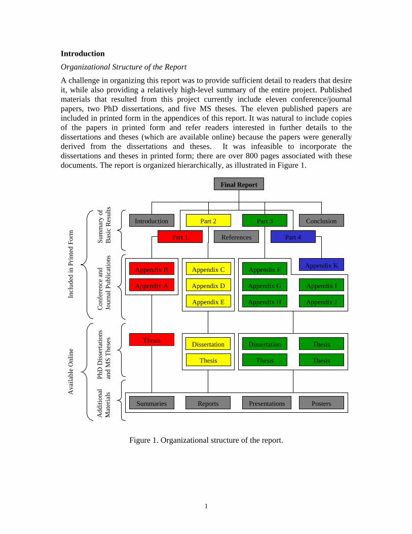
A challenge in organizing this report was to provide sufficient detail to readers that desire it, while also providing a relatively high-level summary of the entire project. Published materials that resulted from this project currently include eleven conference/journal papers, two PhD dissertations, and five MS theses. The eleven published papers are included in printed form in the appendices of this report. It was natural to include copies of the papers in printed form and refer readers interested in further details to the dissertations and theses (which are available online) because the papers were generally derived from the dissertations and theses. It was infeasible to incorporate the dissertations and theses in printed form; there are over 800 pages associated with these documents. The report is organized hierarchically, as illustrated in Figure 1.
Final Report
Introduction Part 2
Part 4
Conclusion
Appendix B
Appendix A
Appendix E
Appendix D
Appendix C
Appendix H
Appendix G
Appendix F
Appendix J
Appendix I
Appendix K
References
Thesis Dissertation
Thesis
Dissertation Thesis
Thesis Thesis
PhD
Dis
serta
tions
an
d M
S Th
eses
Con
fere
nce
and
Jour
nal P
ublic
atio
nsSu
mm
ary
of
Bas
ic R
esul
ts
Summaries Presentations PostersReports
Add
ition
alM
ater
ials
Incl
uded
in P
rinte
d Fo
rmA
vaila
ble
Onl
ine
Part 1
Part 3
Figure 1. Organizational structure of the report.
2
The main body of the report provides a summary of basic results, and includes four major parts: (1) Optimal Multiprocessor Configuration for SAR; (2) Optimal Communication Scheduling for STAP; (3) FPGA Power Prediction and Applications; and (4) Hybrid FPGA/DSP/GPP Platform. Each of these parts is supported by a collection of published papers, theses, and dissertations produced during the project period. Copies of the published papers are included in the appendices of the report. References to these publications are labeled with a number followed by the letter of the appendix where a copy of the publication can be found. For example, reference label [1A] indicates that a copy of the referenced publication can be found in Appendix A. Due to size considerations, copies of theses and dissertations, such as reference [3], are not included in an appendix; however, online links for all references are provided in the list of references. For conference papers, links to the associated presentation materials are also provided within the list of references. As illustrated in Figure 1, additional materials are also available online, including annual project summaries, technical reports, and presentations and posters given at conferences and PI (principal investigator) meetings. Online links to additional materials are provided in the section entitled Additional Materials, which follows the References section.
Each major part is divided into subsections, and each subsection provides an overview of one or more published papers. Overviews of some of the conference papers (e.g., [15I] and [18K]) actually expand upon the publication by including content from the presentation materials associated with that publication. Readers not needing the level of detail found in these overviews are encouraged to first read the Acknowledgments section, which includes a paragraph on the work conducted by each student assistant. Of course readers requiring more detail are encouraged to pursue copies of the papers found in the appendices, online links of presentation materials found in the References section, and/or the online links found in the Additional Materials section. Project Overview
The advantages of using digital signal processing (DSP) chips for high-performance embedded signal processing applications have been demonstrated during the past decade. DSP chips often win over general purpose processors (GPPs) because their complexity (measured, for example, in terms of silicon area, number of transistors, or power consumption) is better matched to the highly regular and numerical-intensive computations required by many signal processing based embedded applications. However, it is now apparent that even DSP chips can be overkill for some computations found in common embedded military applications. That is, in some cases DSP chips are equipped with much more architectural complexity than is actually needed, resulting in inefficiencies and greater power consumption than absolutely necessary.
In this project, we investigated the advantages of integrating configurable hardware together with a multiprocessor DSP/GPP platform. The computational engine of the configurable hardware used in this project was comprised of FPGA chips. A primary goal of our project was to demonstrate that for given computational loads – associated with instances of embedded radar signal processing applications – the total size, weight, and
3
power (SWAP) could be reduced by integrating FPGA-based components as part of the embedded computational platform.
Reconfigurable computing devices, such as FPGAs, can offer a cost-effective and more flexible alternative than the use of application specific integrated circuits (ASICs). FPGAs are especially cost-effective compared to ASICs when only a small number of the chip(s) are required. Another major advantage of FPGAs over ASICs is that they can be reconfigured to change their functionality while still resident in the system, which allows hardware designs to be changed similar to software, and dynamically reconfigured to perform different functions at different times.
A number of theoretical and empirical studies were conducted during the project period to understand and demonstrate the advantages and disadvantages of DSP/GPP versus FPGA technologies with respect to SWAP. A prototype heterogeneous FPGA/DSP/GPP-based platform was constructed using commercial off-the-shelf (COTS) components to demonstrate the utility of a hybrid system containing all three types of technologies. A number of systematic approaches and tools based on mathematical programming and modeling were developed to optimally configure FPGA/DSP/GPP-based platforms for applications in the radar signal-processing domain. The two major applications considered were SAR (synthetic aperture radar) and STAP (space-time adaptive processing).
The prototype system was constructed using COTS components from two vendors: Annapolis Micro Systems, Inc. and Mercury Computer Systems, Inc. We had excellent support from both companies, and we designed and implemented a custom interface to allow communication between two disparate product lines of these vendors. Implementation of a custom interface was necessary because at that time (1997-98) there were few interfacing standards among vendors such as the two we were working with and little customer demand (excluding us, of course!) for providing such an interface. The availability of products and support to more easily interface components from different vendors, including the two we worked with, is much better today. In fact, the output of our research, which illustrated the potential benefits of a hybrid FPGA/DSP/GPP platform, served as a catalyst for these industry sectors to invest significant resources and provide support and standards appropriate for interfacing their product lines. Brief Descriptions of Major Parts of the Report
Part 1: Optimal Multiprocessor Configuration for SAR – describes research for determining optimal multiprocessor configurations for instances of the SAR processing problem. The research was targeted at how to optimally configure a multiprocessor system for given instances of the SAR problem so that the resulting power consumption of the multiprocessor system is minimized. The key to the approach involved making the proper trade-off between the number of processors and amount of memory associated with the multiprocessor configuration. References associated with this work are [1A], [2B], and [3].
4
Part 2: Optimal Communication Scheduling for STAP – describes research for determining how to best schedule inter-processor communications of a parallel STAP algorithm mapped onto a Mercury Race Multiprocessor. The approach is based on a genetic algorithm, and the research also resulted in the development of a fast and accurate network simulator for the RACEway® interconnection network. References associated with this work are [4C], [5D], [6E], [7], and [8].
Part 3: FPGA Power Prediction and Applications – describes mathematical models and other approaches developed for predicting power consumption for FPGA circuits. We found that predicting power consumption for FPGAs was particularly difficult, as it strongly depends on precisely how the chip is configured and the “activity” characteristics of the input data being processed. Nevertheless, we generated new and important results and tools in this area. We also demonstrated the utility of using FPGA circuits for portions of the SAR and STAP applications. References associated with this work are [9F], [10], [11G], [12H], [13], [14], [15I], [16J], and [17].
Part 4: Hybrid FPGA/DSP/GPP Platform – describes a prototype hybrid platform that was constructed for this project. It includes the detailed design and development of the custom interfaces implemented to interconnect the disparate products of the two vendors. Some performance results are also included. The reference associated with this work is [18K].
5
Part 1: Optimal Multiprocessor Configuration for SAR
Overview of References [1A], [2B], and [3]
The real-time embedded application considered in this part, i.e., SAR, as well as many others of military interest, are characterized by a common theme: processing a continuous stream of data collected from radar sensors. The rate at which data samples flow from the sensor(s) to the computational platform is typically very high – often on the order of tens or hundreds of millions of samples per second and even higher. Furthermore, the number of calculations to be performed on each sample is typically at least 100 FLOPs (floating-point operations), which amounts to an overall computational throughput requirement ranging from at least one to ten billion FLOPs (and often much higher).
At the beginning of the contract period, approaches capable of providing a computational platform that could achieve these types of computational throughput rates typically involved a “pipeline of interconnected processors” style of architecture. Such an approach could be a valid and effective architecture in some cases. However, situations often arose in which the throughput requirements dictated that 100 or more SHARC® (or similar) DSP processors were required. In many situations, the associated level of power requirement for the computational platform alone posed a severe problem, because of the strict power budgets available on UAVs (unmanned aerial vehicles) and satellites where these systems are deployed.
In the paper [1A], we showed how a DSP/GPP-based multiprocessor system could be optimally configured using two types of processor/memory daughtercards to minimize overall power consumption for SAR applications. We showed that by careful (and often counterintuitive) selection of parameters associated with both the hardware (the number of daughtercards of two possible types) and the application software (a parameter known as the azimuth section size), an optimal configuration (one with minimal power consumption) can be derived based on the application of mathematical programming techniques.
Our approach centered on the derivation of two mathematical formulas for given instances of the SAR problem: one for the total numbers of processors required and the other for the total memory required. Both of these functions are dependent on the choice of the section size parameter. The derived functions dictate that if a small section size is used, then the associated memory requirements are small, but the processor requirements are high. On the other hand, a large section size was shown to result in a requirement for fewer processors, but more memory.
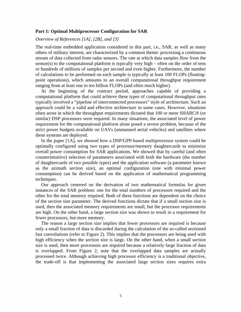
The reason a large section size implies that fewer processors are required is because only a small fraction of data is discarded during the calculation of the so-called sectioned fast convolutions (refer to Figure 2). This implies that the processors are being used with high efficiency when the section size is large. On the other hand, when a small section size is used, then more processors are required because a relatively large fraction of data is overlapped. From Figure 2, note that the overlapped data samples are actually processed twice. Although achieving high processor efficiency is a traditional objective, the trade-off is that implementing the associated large section sizes requires extra
6
memory, and extra memory consumes extra power. It is this inherent trade-off between processor efficiency, memory, and section size that our approach optimized.
Kernel
Discard
OverlapSection
FFT size
Large Overlap/Section ratio ⇒ Small azimuth memory, large number azimuth processorsSmall Overlap/Section ratio ⇒ Large azimuth memory, small number azimuth processors
Figure 2. This diagram illustrates the method of performing sectioned fast convolutions on azimuth input data with a pre-stored kernel. Given that the kernel size is fixed, then if the section size is made large, a relatively small fraction of samples are discarded for each section, thus making processor efficiency high. Conversely, if the section size is small, then a relatively large fraction of samples must be discarded for each section, resulting in poor processor efficiency, but relatively small memory requirements.
The two daughtercards assumed to be available in our approach were: Type 1, which had six SHARC® processors and a total of 32MB of memory; and Type 2, which had two SHARC® processors and a total of 64MB of memory. Thus, our optimization procedure was based on minimizing total consumed power based on proper selection of three parameters: section size, number of Type 1 cards, and number of Type 2 cards. Note that allowing two daughtercards in the configuration put additional constraints on the types of configurations that were possible. Thus, in general, arbitrary numbers of processors and amounts of memory could not me configured. However, the underlying concept of trading the efficiency of processors for more memory was still present.
One interesting lesson learned from our study happened when we considered a situation in which only Type 1 cards were assumed to be available for configuring the system (recall that the Type 1 card is “processor rich” and “memory poor” as compared with the Type 2 card). For this case of configuring only with Type 1 cards, the optimization procedure selected very small section sizes – smaller than one would think to be reasonable. We had to think about why this was happening; it went against our intuition. After some thought, we realized the reason – the objective of our optimization, afterall, was to minimize consumed power, not to maximize processor efficiency. The mathematical programming procedure had no regard for processor efficiency; its only concern was to use the available resources (in this case a lot of processors, and not much memory) to minimize total consumed power. If that means inefficient use of the processors, then so be it.
Consider why it is generally not optimal to force our expectations about what “reasonable” processor efficiencies should be for the case discussed in the previous paragraph. To achieve such efficiencies may require substantial memory (refer to Figure
7
2). So, if “reasonable” processor efficiencies are forced into the configuration, then the number of cards required by the configuration must increase – not because more processors are required, but because more memory is required. In fact, some processors will be idle while the few “efficient ones” are working away – the resource being fully used is the memory. Recall that consumed power is in direct proportion to the number of cards in the configuration. This helped us understand a new interpretation for what our optimization procedure was actually doing: piecing together the “pre-configured silicon” cards available in the most power efficient way possible. Forget about the importance of processor efficiencies that we study/teach in our parallel processing courses!
References [2B] and [3] further refine the results of [1A]. The most notable refinement involves the concept of configuring a compute node. In the Mercury system, a compute node (CN) is an entity on a daughtercard consisting of one or more compute elements (CEs). A compute element, in this context, is a SHARC® processor. In our study, the Type 1 cards were populated with CNs in which each CN contains 3 CEs; and the Type 2 cards were populated with CNs in which each CN contains 2 CEs. In [2B] and [3], we defined formulations to our optimization problem in which the utilization of each CN is determined by the optimization procedure.
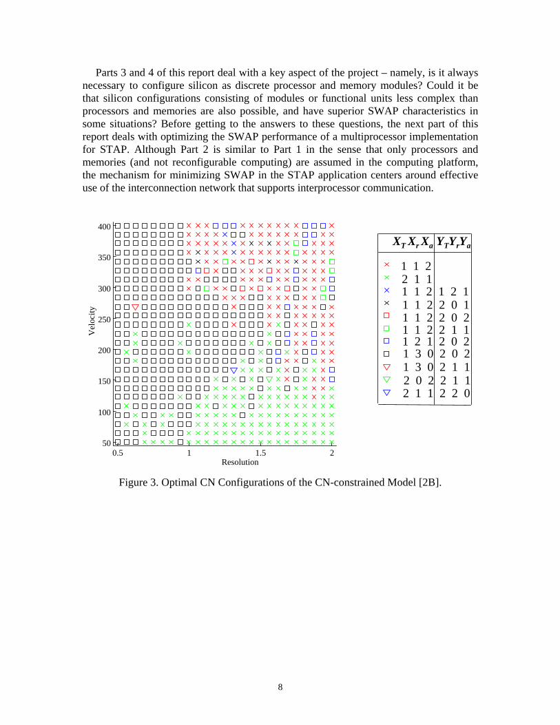
Figure 3 illustrates optimal configurations for a wide range of SAR operating points. The horizontal resolution axis represents the desired SAR image resolution in meters, and the vertical velocity axis is the speed of the vehicle (e.g., UAV) in meters/sec. The legend on the right side of the figure indicates two possible choices (X and Y) for CN configurations. The value of XT and YT indicate the card Type (1 or 2) selected for the X and Y configurations. For example, the red square symbol ‘ ’ is associated with the use of card Type 1 for the X configuration (i.e., XT = 1) and card Type 2 for the Y configuration (i.e., YT = 2). Furthermore, for the X configuration, one CE (for each CN) is utilized for range processing (i.e., Xr =1) and two CEs are used for azimuth processing (i.e., Xa = 2). Similarly, for the Y configuration, none of the CEs are used for range processing, and both CEs (for each CN) are used for azimuth processing (because Yr = 0 and Ya = 2). For the sake of comparison, consider now the configurations associated with the blue times symbol ‘×’ where both the X and Y configurations use the Type 1 card, but the utilization of the CNs for X and Y are distinct. The number of configured CNs, and thus the total number of cards of each type, is also provided by the optimization procedure, but is not shown on Figure 3.
Although subtle, perhaps, this part of the work is extremely important because it cuts to the heart of a bigger issue. The most fundamental questions of interest for these types of systems should not necessarily be expressed in terms of processor efficiencies, or even processors or memories at all; what is important is the “configuration of the silicon,” i.e., how can it be configured to minimize SWAP. The mixing of the two card types we studied is only a rough approximation to this general concept of “configurable silicon.” With two discrete card types available, many, but not anywhere near all, possible combinations of processors and memories can be configured. But remember, processors and memory are not the only things we can build out of silicon. More specialized functional units can also be built.
8
Parts 3 and 4 of this report deal with a key aspect of the project – namely, is it always necessary to configure silicon as discrete processor and memory modules? Could it be that silicon configurations consisting of modules or functional units less complex than processors and memories are also possible, and have superior SWAP characteristics in some situations? Before getting to the answers to these questions, the next part of this report deals with optimizing the SWAP performance of a multiprocessor implementation for STAP. Although Part 2 is similar to Part 1 in the sense that only processors and memories (and not reconfigurable computing) are assumed in the computing platform, the mechanism for minimizing SWAP in the STAP application centers around effective use of the interconnection network that supports interprocessor communication.
0.5 1 1.5 250
100
150
200
250
300
350
400
Resolution
Vel
ocity
1 1 22 1 11 1 2 1 2 1
XT Xr Xa YTYrYa
1 1 2 2 0 1
1 2 1 2 0 21 3 0 2 0 21 3 0 2 1 12 0 2 2 1 1
1 1 2 2 1 1
2 1 1 2 2 0
1 1 2 2 0 2
Figure 3. Optimal CN Configurations of the CN-constrained Model [2B].
9
Part 2: Optimal Communication Scheduling for STAP
Overview of References [4C], [5D], [6E], [7], and [8]
The work here develops and evaluates a genetic-algorithm-based (GA-based) optimization technique for the scheduling of messages for a class of parallel embedded signal processing techniques known as space-time adaptive processing (STAP). The GA-based optimization is performed off-line, resulting in static schedules for the compute nodes of the parallel system. These schedules are utilized for the on-line implementation of the parallel STAP application. The primary motivation and justification for devoting significant off-line effort to solving the formulated scheduling problem is the resulting reduction of hardware resources required for the actual on-line implementation. Studies illustrate that reductions in hardware requirements of around 50% can be achieved by employing the results of the proposed scheduling techniques. This reduction in hardware requirement is of critical importance for STAP, which is typically an airborne application in which the size, weight, and power consumption of the computational platform are often severely constrained.
For an application implemented on a parallel and embedded system to achieve required performance, it is important to effectively map the tasks of the application onto the processors in a way that reduces the volume of inter-processor communication traffic. It is also important to schedule the communication of the required message traffic in a manner that minimizes network contention so as to achieve the smallest possible communication times.
Mapping and scheduling can both – either independently or in combination – be cast as optimization problems, and optimizing mapping and scheduling objectives can be critical to the performance of the overall system. For embedded applications, great importance is often placed on determining minimal hardware requirements that can support a number of different application scenarios. This is because there are typically tight constraints on the amount of hardware that can be accommodated within the embedded platform. Using mappings and schedules that minimize the communication time of parallel and embedded applications can increase the overall efficiency of the parallel system, thus leading to reduced hardware requirements for a given set of application scenarios.
The work here focuses on using a GA-based approach to optimize the scheduling of messages for STAP algorithms. STAP is an adaptive signal processing method that simultaneously combines signals received from multiple elements of an antenna array (the spatial domain) and from multiple pulses (the temporal domain) of a coherent processing interval. The focus of this research assumes STAP is implemented using an element-space post-Doppler partially adaptive algorithm; refer to references [6E], [7], and [8] for details.
STAP involves signal processing methods that operate on data collected from a set of spatially distributed sensors over a given time interval. Signal returns are composed of range, pulse, and antenna-element digital samples; consequently, a three-dimensional (3-D) data cube naturally represents STAP data. A distributed memory multiprocessor
10
machine is assumed here for the parallel STAP implementation. The core processing requirement proceeds in three distinct phases of computation, one associated with each dimension of the STAP data cube. After each phase of processing, the data must be re-distributed across the processors of the machine, which represents the communication requirements of this parallel application. Thus, there are two primary phases of inter-processor data communication required: one between the first and second phases of processing and one between the second and third phases of processing. After all three phases of processing are complete for a given STAP data cube, a new data cube is input into the parallel machine for processing.
A proposed GA-based approach is used to solve the message-scheduling problem associated with each of the two phases of inter-processor data communication. This GA-based optimization is performed off-line, and the results of this optimization are static schedules for the compute nodes of the parallel system. These schedules are used within the on-line parallel STAP implementation. The results of the study show that significant improvements in communication time performance are possible using the proposed approach for scheduling. It is then shown that these improvements in communication time translate to reductions in required hardware for a class of scenarios. Performance of the mappings and schedules are evaluated based on a Mercury RACEway® network simulator developed under this project and described in references [4C] and [7].
For this work, the STAP data cube is partitioned into sub-cube bars of vectors where each vector is mapped onto a given CN (compute node), refer to [6E] for more details. A two-dimensional process set, as described in [8], defines the mapping of data onto CNs for each computational phase. Additionally, the process set defines the communication pattern for the required “distributed corner turns” of the STAP data cube.
Summarizing the results published in [6E] and [8], it is demonstrated that off-line GA-based message scheduling can significantly improve the communication performance in a parallel system. When compared to baseline and randomly generated schedules, the GA-based schedules are significantly superior – typically reducing communication times by between 20% and 50%, see [8] for details.
Interestingly, it is shown that the best mapping – defined as a mapping that minimizes a mapping objective function – is not always the best choice in terms of minimizing overall communication time. In particular, as the number of CNs is increased, optimal mappings that require only one phase of communication generally report higher overall communication times than those good (but not optimal) mappings that require two non-trivial phases of communication.
The optimization of mapping and scheduling, either independently or in combination, is critical to the performance of the STAP application for embedded parallel systems. For such systems, great significance is placed on minimizing overall execution time, which includes both computation and communication components. Such reductions in execution time also translate into improved hardware efficiency and thus reduced hardware requirements, which is often critical.
Through extensive numerical studies, it is shown in [6E] and [8] that the GA-based optimization approaches can yield mappings and schedules that greatly improve the on-
11
line performance and reduce the hardware requirements of the parallel embedded system. Examples are provided that illustrate the optimal mapping and scheduling methodologies of [6E] and [8] can produce hardware savings of 50% and more when compared to typical solutions to the mapping and scheduling problems that might be employed by practitioners. Because of limitations on the size of problems that were executed/simulated, systems up to a size of only 32 processors were investigated. However, from the trends observed in overall completion times, it is apparent that even more significant savings in hardware/power requirements are realizable for STAP applications that require substantially larger systems having hundreds or even thousands of processors.
12
Part 3: FPGA Power Prediction and Applications
We discovered during the project period that predicting power consumption for an FPGA is a very difficult task. There were no commercially available tools that accurately predicted power consumption for any of the existing FPGAs. Thus, a major focus of this part of the work involved the development of accurate methods for predicting FPGA power consumption. References generated by this project in the area of power prediction include [9F], [10], and [11G], which are overviewed in Section 3.1.
In addition to trying to understand and predict FPGA power consumption, we also studied the types of computations that could be effectively mapped onto FPGAs. In theory, given enough gates, one could imagine configuring an FPGA board to behave as a microprocessor. Thus, again in theory, an FPGA board could be used to perform any type of calculation. However, based on the available technology, this would be extremely impractical. Our goal was to therefore use FPGAs to devise useful modules that are much less complex than a microprocessor, thereby reducing the SWAP overhead inherent when computations are performed only on microprocessors and/or DSPs. So, one of our aims was to characterize the types of computations that can be practically implemented in FPGAs. References produced in the area of mapping applications onto FPGAs include [12H], [13], [14], [15I], [16J], and [17], and these are overviewed in Section 3.2. 3.1 FPGA Power Prediction
Overview of References [9F] and [10]
The work published in [9F] and [10] describes a practical and accurate power prediction tool for the Xilinx® 4000-series FPGA. The utility of the tool is that it enables FPGA circuit designers to evaluate the power consumption of their designs without resorting to the laborious and expensive empirical approach of instrumenting an FPGA board/chip and/or taking actual power consumption measurements. Preliminary evaluation of the tool indicates that an error of less than 5% is usually achieved when compared with actual physical measurements of power consumption.
The tool, which is implemented in Java, takes as input two files: (1) a configuration file associated with an FPGA design and (2) a pin file that characterizes the signal activities of the input data pins to the FPGA. The configuration file defines how each CLB (configurable logic block) is programmed and defines signal connections among the programmed CLBs. The configuration file is a text file that is generated using a Xilinx® M1 Foundation Series utility called ncdread. The pin file is also a text file, but is generated by the user. It contains a listing of pins that are associated with the input data for the configured FPGA circuit. For each pin number listed, probabilistic parameters are provided which characterize the signal activity for that pin.
Based on the two input files, the tool propagates the probabilistic information associated with the pins through a model of the FPGA configuration and calculates the activity of every internal signal associated with the configuration. The activity of an internal signal s, denoted as, is a value between zero and one and represents the signal’s
13
relative frequency with respect to the frequency of the system clock, f. Thus, the average frequency of signal s is given by as f.
Computing the activities of the internal signals represents the bulk of computations performed by the tool. Given the probabilistic parameters for all input signals of a configured CLB, the probabilistic parameters of that CLB’s output signals are determined using a mathematical transformation. Thus, the probabilistic information for the pin signals is transformed as it passes through the model of the configured logic, defined by the configuration file. However, the probabilistic parameters of some CLB inputs may not be initially known because they are not directly connected to pin signals, but instead are connected to the output of another CLB for which the output probabilistic parameters have not yet been computed (i.e., there is a feedback loop). For this reason, the tool applies an iterative approach to update the values for unknown signal parameters. The iteration process continues until convergence is reached, which means that the determined signal parameters are consistent based on the mathematical transformation that relates input and output signal parameter values, for every CLB.
The average power dissipation due to a signal s is modeled by ½ Cd(s)V 2as f, where d(s) is the Manhattan distance the signal s spans across the array of CLBs, Cd(s) is the equivalent capacitance seen by the signal s, and V is the voltage level of the FPGA device. The overall power consumption of the configured device is the sum of the power dissipated by all signals of the configured FPGA.
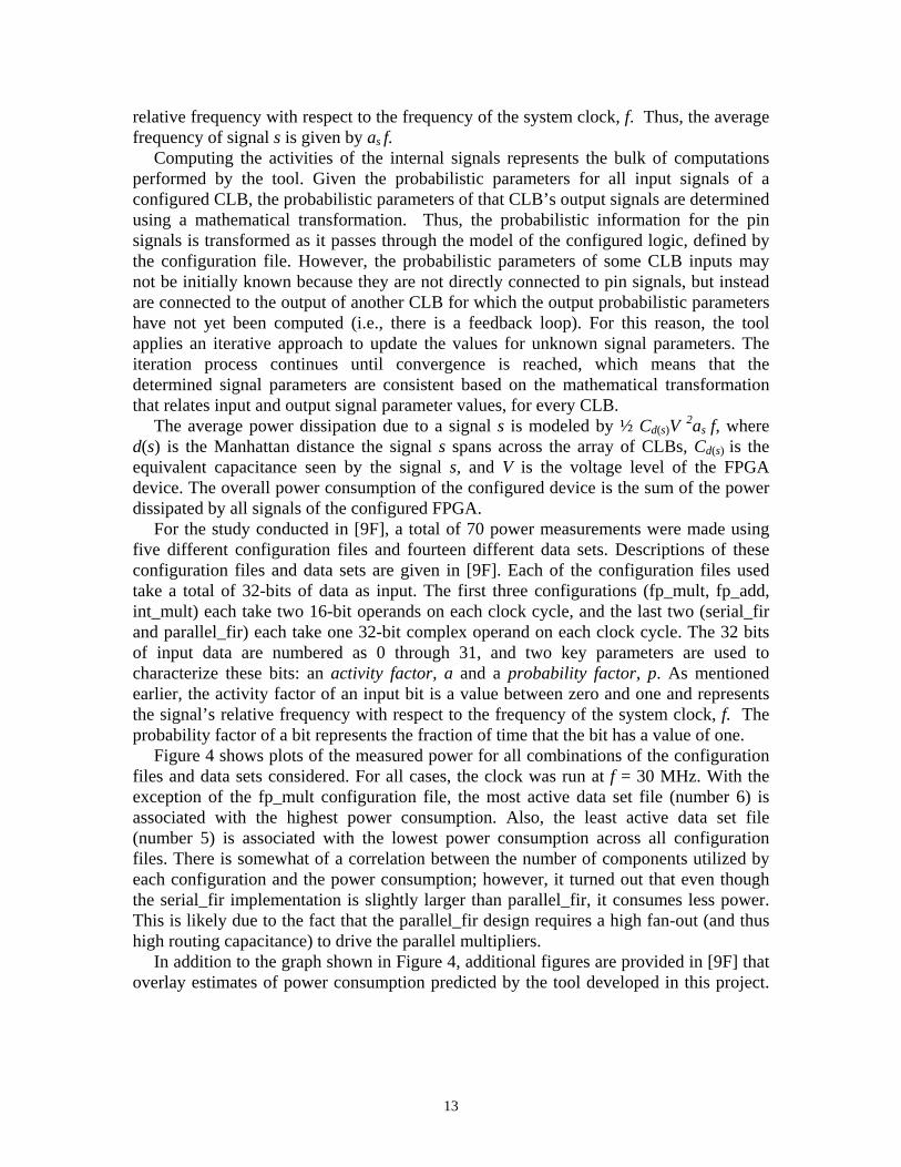
For the study conducted in [9F], a total of 70 power measurements were made using five different configuration files and fourteen different data sets. Descriptions of these configuration files and data sets are given in [9F]. Each of the configuration files used take a total of 32-bits of data as input. The first three configurations (fp_mult, fp_add, int_mult) each take two 16-bit operands on each clock cycle, and the last two (serial_fir and parallel_fir) each take one 32-bit complex operand on each clock cycle. The 32 bits of input data are numbered as 0 through 31, and two key parameters are used to characterize these bits: an activity factor, a and a probability factor, p. As mentioned earlier, the activity factor of an input bit is a value between zero and one and represents the signal’s relative frequency with respect to the frequency of the system clock, f. The probability factor of a bit represents the fraction of time that the bit has a value of one.
Figure 4 shows plots of the measured power for all combinations of the configuration files and data sets considered. For all cases, the clock was run at f = 30 MHz. With the exception of the fp_mult configuration file, the most active data set file (number 6) is associated with the highest power consumption. Also, the least active data set file (number 5) is associated with the lowest power consumption across all configuration files. There is somewhat of a correlation between the number of components utilized by each configuration and the power consumption; however, it turned out that even though the serial_fir implementation is slightly larger than parallel_fir, it consumes less power. This is likely due to the fact that the parallel_fir design requires a high fan-out (and thus high routing capacitance) to drive the parallel multipliers.
In addition to the graph shown in Figure 4, additional figures are provided in [9F] that overlay estimates of power consumption predicted by the tool developed in this project.
14
As mentioned above, predicted values of power were generally within 5% of actual measured values.
0 2 4 6 8 10 12 14
2.0
2.5
3.0
3.5
4.0
4.5
5.0 Configure f iles: fp_mult fp_add int_mult serial_fir parallel_f ir
Powe
r Con
sum
ptio
n (w
)
data sets
Figure 4. Measured power consumption of the configuration files and data sets from [9F].
Overview of Reference [11G]
The method used by the above tool to compute signal activities was based on a previously published approach from another research group. That approach has some difficulties, primarily related to its time complexity. In [11G], a new analytical approach was developed by us for calculating signal activities. Our approach is based on a Markov chain signal model, and directly accounts for correlations present among the signals. We verified the accuracy of the approach by comparing signal activity values calculated using our approach with corresponding values produced through simulation studies. It was also demonstrated that the proposed approach is much more computationally efficient than competing approaches. In addition to describing the new approach for calculating signal activities, [11G] also provides a comprehensive review of past approaches, including the approach implemented for the tool described in [9F] and [10]. 3.2 FPGA Applications
Overview of References [12H] and [13]
In references [12H] and [13], techniques for mapping portions of space-time adaptive processing (STAP) computations onto FPGAs are described. The output of STAP is a weighted sum of multiple radar returns, where the weights for each return in the sum are calculated adaptively and in real-time. The most computationally intensive portion of most STAP approaches is the calculation of the adaptive weight values, which typically
15
constitutes over 90% of all the computations needed in adaptive processing. Calculation of the weights involves solving a set of linear equations based on an estimate of the covariance matrix associated with the radar return data. The traditional approach for computing the adaptive weights is based on a direct method called QR-decomposition. This method has a fixed computational complexity, which depends on the size of the equation matrix and provides the exact solution. An alternative approach based on an iterative method called Conjugate Gradient was investigated, which allows for trading off accuracy for reduced computational complexity. The two approaches are analyzed and compared in [13]. The results show that the Conjugate Gradient approach can reduce the computations needed at the cost of reduced accuracy in some cases.
Existing computational strategies for STAP typically rely exclusively on the use of multiple DSPs and/or GPPs. An alternative strategy is proposed in [12H] and [13], which makes use of FPGAs as vector co-processors that perform inner product calculations. Two different “inner-product co-processor” designs are introduced for use with a host DSP or GPP. The first has a multiply-and accumulate structure and the second uses a reduction-style tree structure having two multipliers and an adder. For a fixed clock rate, the second design can provide a higher throughput, but requires more computation from the host (to perform the final summation of the partial sums).
In the work of [12H] and [13], the two inner-product co-processors were implemented using a block floating point format, which is much simpler to implement than standard floating point units. We also investigated overall accuracy of block floating point versus full floating point. It was demonstrated that the block floating point co-processors produce acceptable accuracy results for input data distributions that are uniformly distributed. Poor results are obtained, however, for cases where one or a few of the elements are much larger than the rest of the numbers. This is because the block-floating-point architecture normalizes all the exponents to the maximum exponent by shifting out the least significant bits of the mantissa so that all the exponents are equal, and then all the operations are integer arithmetic operations (based on the resulting mantissas), which are much easier to perform than general floating-point operations. The shifting out of the bits produces inaccuracy in the computations. For all the ranges of numbers considered, if the numbers are uniformly distributed, then the exponent distribution has an increasing exponential shape with a majority of the numbers close to the maximum value in the exponent domain. This results in a small number of bits from the mantissas of the numbers being shifted out, on the average. Another important point is that the multiply implementation uses a 15-bit mantissa, which implies that the mantissa of the input floating-point number is truncated to 15 bits from 23 bits, which itself introduces some inaccuracies. Overview of Reference [14]
In reference [14], further studies of inner-product co-processor designs were conducted. In contrast to the inner product designs of [12H] and [13], which were based on a block floating point format, both floating point and integer formats were used in [14], both using 16-bit formats. The studies demonstrated that inner-product co-processors, for both
16
integer and floating-point data, could fit into current (at that time) FPGA technology and achieve significant speed and throughput. The results of the implementations show that it is feasible and beneficial under certain circumstances to implement floating-point and integer operations in FPGAs (i.e., such as when a custom data format can be used, as with the SHARC® DSP which can convert back and forth between IEEE 32-Bit floating point and the SHARC® DSP 16-bit floating point formats).
The studies in [14] also considered the advantages and disadvantages of employing different degrees of pipelining in the inner product designs. One interesting (and somewhat counterintuitive) outcome related to pipelined versions of the designs was that adding more pipeline stages did not always allow for an increased clock speed at which the circuit could be executed. This was due to the fact that adding in the pipeline stages also added more overall complexity, which made it more difficult for the place-and-route routines of the FPGA design tool to find good implementations. Thus, as more pipelined stages were added, critical signal lengths sometimes increased, dictating that the clock rate actually had to be decreased. Estimates of power consumption were also evaluated for all designs considered in [14].
Overview of Reference [15I]
Two major contributions are presented in [15I]. First, it is shown that the core computations from the SAR application, including both the range compression and azimuth processing phases, can be structured as a single deep computational pipeline that can be implemented directly on an array of FPGAs. Past results for high-throughput SAR processing (e.g., refer to [1A], [2B], and [3]) typically assume the computations are to be mapped onto a distributed memory multiprocessor system in which a subset of the available compute elements (CEs) is assigned to perform range processing and the remaining CEs perform azimuth processing. In this type of traditional approach, a number of processed range vectors are sent from the range CEs to the azimuth CEs where they are buffered in memory. After a prescribed number of compressed range vectors are present in the memory space of the azimuth CEs, azimuth processing commences on the azimuth CEs. Because of the significant intermediate buffer storage required by this approach, and the associated placing and fetching of data in this memory space by the range and azimuth CEs, respectively, this type of SAR implementation is generally not thought to be “purely streaming.” However, as is presented in [15I], these computations (both phases) can in fact be structured as a single computational pipeline, which can be directly mapped onto an array of FPGAs.
In the proposed approach, no intermediate memory buffer is required between the two phases of computation. Instead, within the structure of the computational pipeline are long segments of delay elements that effectively provide the intermediate storage associated with the more traditional approach. Figure 5 illustrates the structure of the computational pipeline. In the figure, small values of parameters are used for the purpose minimizing the size of the pipeline, while still illustrating its basic structure. Realistic parameters values would be on the order of thousands, resulting in a pipeline with millions of registers. Further details on sizing analysis and hardware comparisons
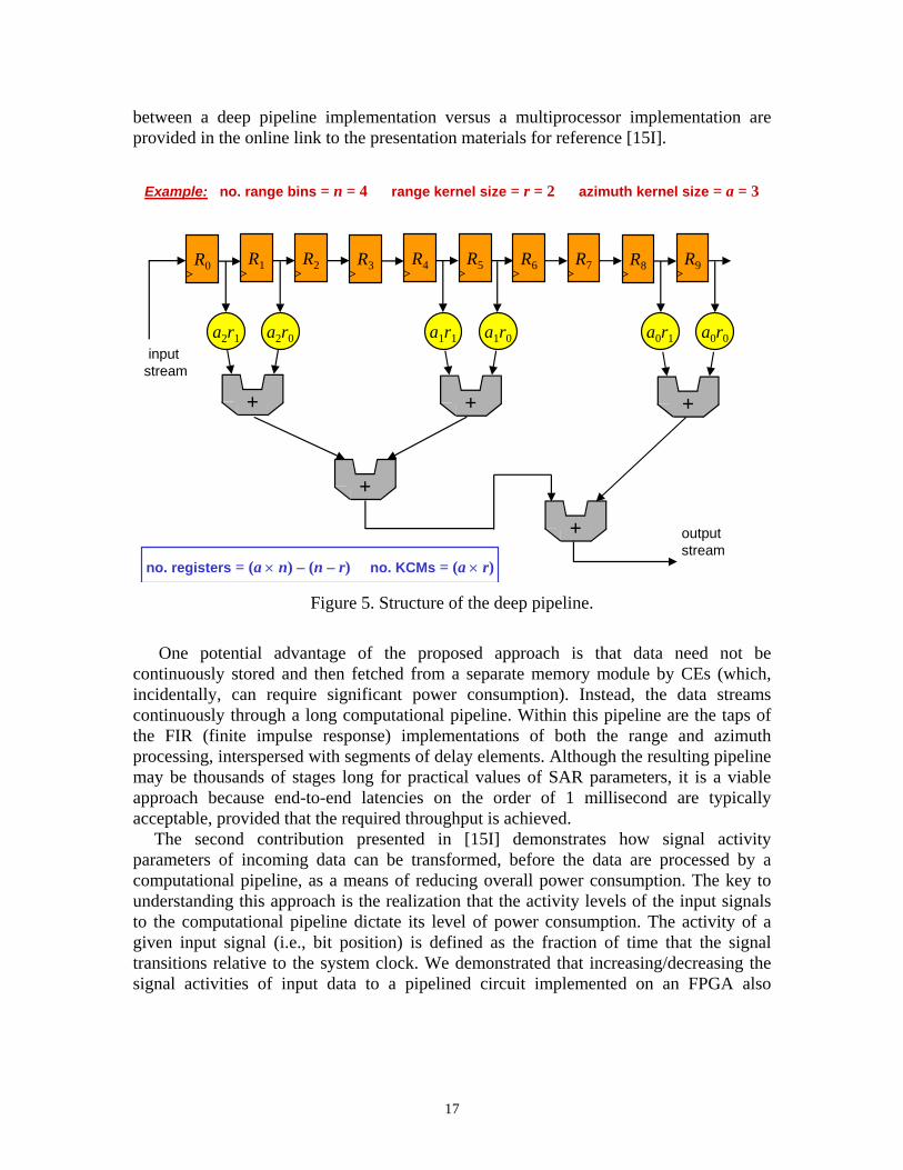
17
between a deep pipeline implementation versus a multiprocessor implementation are provided in the online link to the presentation materials for reference [15I].
a2r1 a2r0 a1r1 a1r0 a0r1 a0r0
Example: no. range bins = n = 4 range kernel size = r = 2 azimuth kernel size = a = 3
R0>
R1>
R2>
R3>
R4>
R5>
R6>
R7>
R8>
R9>
+
input stream
output stream
+ +
+
+
no. registers = (a × n) – (n – r) no. KCMs = (a × r) Figure 5. Structure of the deep pipeline.
One potential advantage of the proposed approach is that data need not be
continuously stored and then fetched from a separate memory module by CEs (which, incidentally, can require significant power consumption). Instead, the data streams continuously through a long computational pipeline. Within this pipeline are the taps of the FIR (finite impulse response) implementations of both the range and azimuth processing, interspersed with segments of delay elements. Although the resulting pipeline may be thousands of stages long for practical values of SAR parameters, it is a viable approach because end-to-end latencies on the order of 1 millisecond are typically acceptable, provided that the required throughput is achieved.
The second contribution presented in [15I] demonstrates how signal activity parameters of incoming data can be transformed, before the data are processed by a computational pipeline, as a means of reducing overall power consumption. The key to understanding this approach is the realization that the activity levels of the input signals to the computational pipeline dictate its level of power consumption. The activity of a given input signal (i.e., bit position) is defined as the fraction of time that the signal transitions relative to the system clock. We demonstrated that increasing/decreasing the signal activities of input data to a pipelined circuit implemented on an FPGA also
18
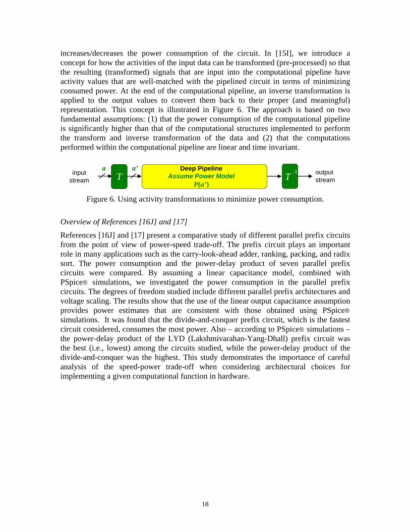
increases/decreases the power consumption of the circuit. In [15I], we introduce a concept for how the activities of the input data can be transformed (pre-processed) so that the resulting (transformed) signals that are input into the computational pipeline have activity values that are well-matched with the pipelined circuit in terms of minimizing consumed power. At the end of the computational pipeline, an inverse transformation is applied to the output values to convert them back to their proper (and meaningful) representation. This concept is illustrated in Figure 6. The approach is based on two fundamental assumptions: (1) that the power consumption of the computational pipeline is significantly higher than that of the computational structures implemented to perform the transform and inverse transformation of the data and (2) that the computations performed within the computational pipeline are linear and time invariant.
Deep Pipeline
Assume Power ModelP(a’)
input stream
output stream
-1TTa a’
Figure 6. Using activity transformations to minimize power consumption.
Overview of References [16J] and [17]
References [16J] and [17] present a comparative study of different parallel prefix circuits from the point of view of power-speed trade-off. The prefix circuit plays an important role in many applications such as the carry-look-ahead adder, ranking, packing, and radix sort. The power consumption and the power-delay product of seven parallel prefix circuits were compared. By assuming a linear capacitance model, combined with PSpice® simulations, we investigated the power consumption in the parallel prefix circuits. The degrees of freedom studied include different parallel prefix architectures and voltage scaling. The results show that the use of the linear output capacitance assumption provides power estimates that are consistent with those obtained using PSpice® simulations. It was found that the divide-and-conquer prefix circuit, which is the fastest circuit considered, consumes the most power. Also – according to PSpice® simulations – the power-delay product of the LYD (Lakshmivarahan-Yang-Dhall) prefix circuit was the best (i.e., lowest) among the circuits studied, while the power-delay product of the divide-and-conquer was the highest. This study demonstrates the importance of careful analysis of the speed-power trade-off when considering architectural choices for implementing a given computational function in hardware.
19
Part 4: Hybrid FPGA/DSP/GPP Platform
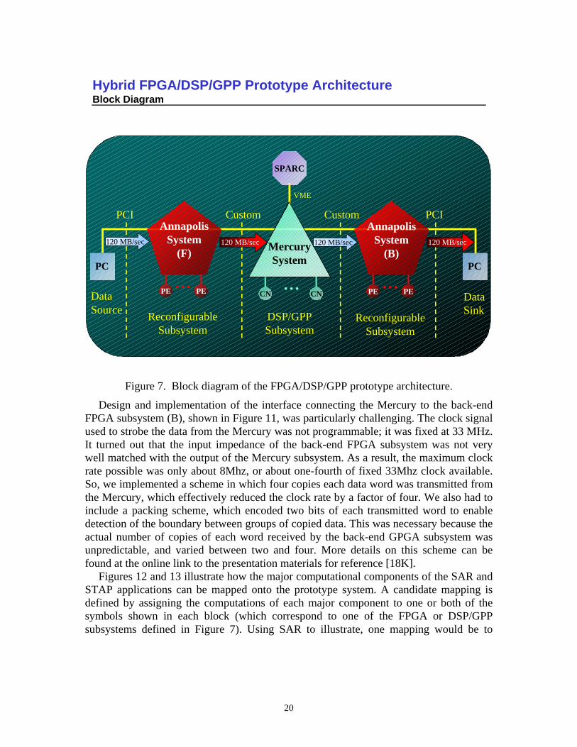
Overview of Reference [18K]
The prototype platform was developed to demonstrate the advantages and trade-offs associated with the combined use of different hardware technologies for two embedded radar-processing applications, namely SAR and STAP. The primary metrics of interest are size, weight, and power utilizations. The developed system can be configured with FPGAs, DSPs, and/or GPPs. Although the prototype system was not evaluated through fielded studies, experiments involving continuous input streams at relatively high rates were conducted in the laboratory using unprocessed radar data as input.
The FPGA components of the prototype system are commercially available WildOneTM and WildForceTM boards (from Annapolis Microsystems) populated with 4000-series Xilinx® parts. The WildForceTM boards each have four 4085-series FPGAs plus one control FPGA. The DSP/GPP components of the system are within a Mercury Race Multicomputer configured with both SHARC® and PowerPC® CNs. The Mercury system can be configured with up to eight PowerPC® nodes and eight SHARC® compute nodes (each SHARC® CN actually contains three SHARC® DSP chips).
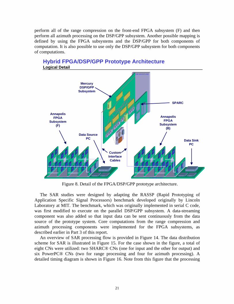
An overview of the overall architecture is depicted in Figure 7. A more detailed view of the major components of the hybrid system are illustrated in Figure 8, and a photograph of the actual prototype system is provided in Figure 9.
The source PC is responsible for initially loading unprocessed radar data (from disk) into a circular buffer within its main memory. Once the input data is loaded into the circular buffer, the source PC then continuously (and repeatedly) streams this data into the front-end FPGA subsystem, denoted as (F) in Figures 7, 8, and 9. It was necessary to locate the input data in a large main memory buffer in order to achieve realistic data throughput rates, which would otherwise not be possible if the data were streamed directly from the disk of the source PC. All of the Annapolis FPGA boards are PCI-based and reside on the data source and/or data sink PCs. A total of four WildForceTM boards are available, and zero or more of these may reside on the source and sink PCs. The source and sink PCs also contain one WildOneTM board each. The WildOneTM boards are not used for computation; they handle the data communication (through the PCI bus) between the PCs and the FPGA subsystems. The data communication among all FPGA boards is through two types of 36-bit wide connectors, one called systolic and one called SIMD.
The data communication between the front-end FPGA subsystem (F) and the DSP/GPP subsystem is a custom interface developed using the systolic connector from Annapolis and the RIN-T input device from Mercury. Similarly, the data communication between the DSP/GPP subsystem and the back-end FPGA subsystem (B) is through a custom interface developed using the ROUT-T output device from Mercury and the systolic connector from Annapolis. More details on the design of the interfaces between the Mercury and the front- and back-end subsystems are provided in Figures 10 and 11, respectively.
20
Data Source
VME
MercurySystem
CNCNPEPE... ...
SPARC
ReconfigurableSubsystem
DSP/GPPSubsystem
Data Sink
AnnapolisSystem
(F)120 MB/sec
PC
120 MB/sec120 MB/sec
PC
PCI Custom Custom
PEPE...
ReconfigurableSubsystem
AnnapolisSystem
(B)
PCI
120 MB/sec
Hybrid FPGA/DSP/GPP Prototype ArchitectureBlock Diagram
Figure 7. Block diagram of the FPGA/DSP/GPP prototype architecture.
Design and implementation of the interface connecting the Mercury to the back-end FPGA subsystem (B), shown in Figure 11, was particularly challenging. The clock signal used to strobe the data from the Mercury was not programmable; it was fixed at 33 MHz. It turned out that the input impedance of the back-end FPGA subsystem was not very well matched with the output of the Mercury subsystem. As a result, the maximum clock rate possible was only about 8Mhz, or about one-fourth of fixed 33Mhz clock available. So, we implemented a scheme in which four copies each data word was transmitted from the Mercury, which effectively reduced the clock rate by a factor of four. We also had to include a packing scheme, which encoded two bits of each transmitted word to enable detection of the boundary between groups of copied data. This was necessary because the actual number of copies of each word received by the back-end GPGA subsystem was unpredictable, and varied between two and four. More details on this scheme can be found at the online link to the presentation materials for reference [18K].
Figures 12 and 13 illustrate how the major computational components of the SAR and STAP applications can be mapped onto the prototype system. A candidate mapping is defined by assigning the computations of each major component to one or both of the symbols shown in each block (which correspond to one of the FPGA or DSP/GPP subsystems defined in Figure 7). Using SAR to illustrate, one mapping would be to
21
perform all of the range compression on the front-end FPGA subsystem (F) and then perform all azimuth processing on the DSP/GPP subsystem. Another possible mapping is defined by using the FPGA subsystems and the DSP/GPP for both components of computation. It is also possible to use only the DSP/GPP subsystem for both components of computations.
PCI MOTHER BOARDPENTIUM DRAM
WIL
D
ON
E
SRAM
SRA
M
AN
NA
POLI
S
WIL
DFO
RC
E
AN
NA
POLI
S
WIL
DFO
RC
E
AN
NA
POLI
S
WIL
DFO
RC
E
AN
NA
POLI
S
WIL
DFO
RC
E
HARD DISK DRIVE
Hybrid FPGA/DSP/GPP Prototype ArchitectureLogical Detail
PCI MOTHER BOARDPENTIUM DRAM
WIL
D
ON
E
SRA
M
SR
AM
AN
NA
POLI
S
WIL
DFO
RC
E
AN
NA
POLI
S
WIL
DFO
RC
E
AN
NA
POLI
S
WIL
DFO
RC
E
AN
NA
POLI
S
WIL
DFO
RC
E
HARD DISK DRIVE
CN C
N CN
CN C
N CN C
N
CN C
N
CN C
N CN C
N
CN
DR
AM
ASIC
RIN
-T
VME BACKPLANE
MER
CU
RY
RA
CE
MC
H 9
U B
OA
RD
HAR
D D
ISK
DR
IVE
DR
AMSP
ARC
RO
UT-
T FOR
CE
SPA
RC
5V
CN
Data SourcePC
AnnapolisFPGA
Subsystem(F)
Custom Interface Cables
SPARC
MercuryDSP/GPP
Subsystem
Data SinkPC
AnnapolisFPGA
Subsystem(B)
Figure 8. Detail of the FPGA/DSP/GPP prototype architecture.
The SAR studies were designed by adapting the RASSP (Rapid Prototyping of
Application Specific Signal Processors) benchmark developed originally by Lincoln Laboratory at MIT. The benchmark, which was originally implemented in serial C code, was first modified to execute on the parallel DSP/GPP subsystem. A data-streaming component was also added so that input data can be sent continuously from the data source of the prototype system. Core computations from the range compression and azimuth processing components were implemented for the FPGA subsystems, as described earlier in Part 3 of this report.
An overview of SAR processing flow is provided in Figure 14. The data distribution scheme for SAR is illustrated in Figure 15. For the case shown in the figure, a total of eight CNs were utilized: two SHARC® CNs (one for input and the other for output) and six PowerPC® CNs (two for range processing and four for azimuth processing). A detailed timing diagram is shown in Figure 16. Note from this figure that the processing
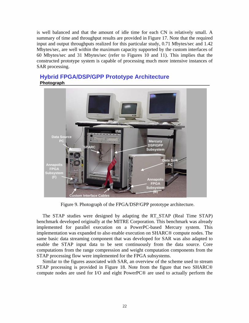
22
is well balanced and that the amount of idle time for each CN is relatively small. A summary of time and throughput results are provided in Figure 17. Note that the required input and output throughputs realized for this particular study, 0.71 Mbytes/sec and 1.42 Mbytes/sec, are well within the maximum capacity supported by the custom interfaces of 60 Mbytes/sec and 31 Mbytes/sec (refer to Figures 10 and 11). This implies that the constructed prototype system is capable of processing much more intensive instances of SAR processing.
Hybrid FPGA/DSP/GPP Prototype ArchitecturePhotograph
Data SinkPC
Data SourcePC
Custom Interface Cables
MercuryDSP/GPP
Subsystem
AnnapolisFPGA
Subsystem(F) Annapolis
FPGASubsystem
(B)
SPARC
Figure 9. Photograph of the FPGA/DSP/GPP prototype architecture.
The STAP studies were designed by adapting the RT_STAP (Real Time STAP)
benchmark developed originally at the MITRE Corporation. This benchmark was already implemented for parallel execution on a PowerPC-based Mercury system. This implementation was expanded to also enable execution on SHARC® compute nodes. The same basic data streaming component that was developed for SAR was also adapted to enable the STAP input data to be sent continuously from the data source. Core computations from the range compression and weight computation components from the STAP processing flow were implemented for the FPGA subsystems.
Similar to the figures associated with SAR, an overview of the scheme used to stream STAP processing is provided in Figure 18. Note from the figure that two SHARC® compute nodes are used for I/O and eight PowerPC® are used to actually perform the
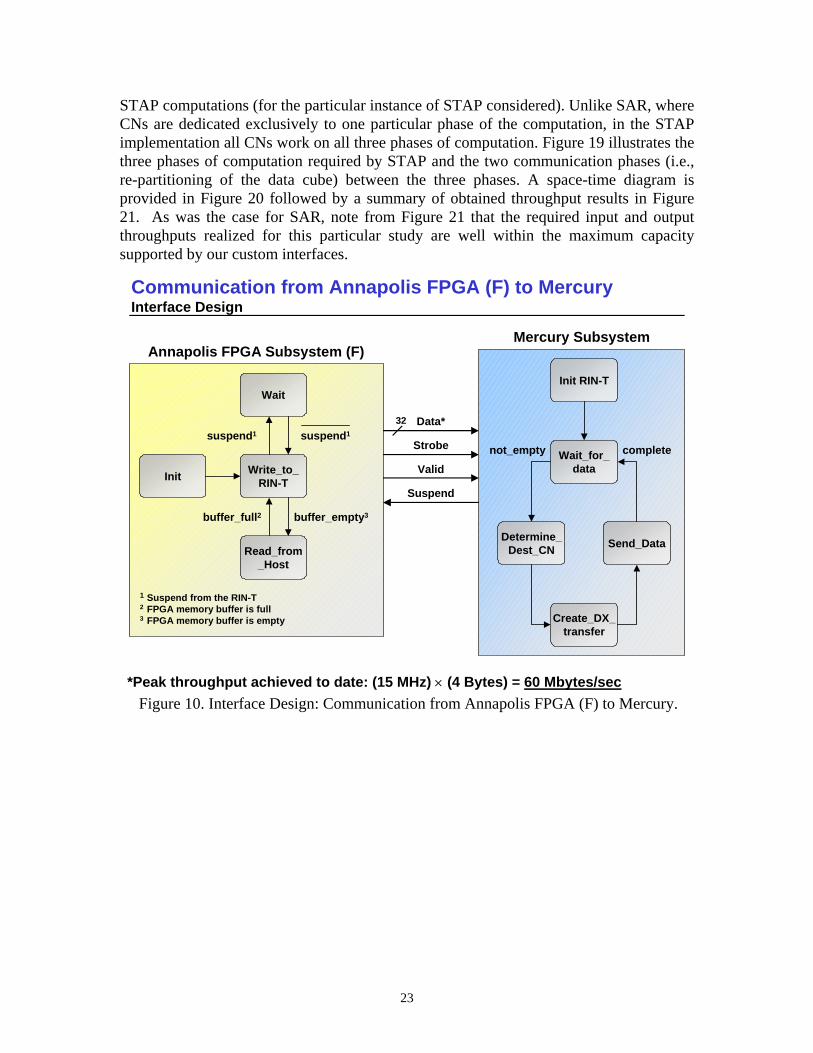
23
STAP computations (for the particular instance of STAP considered). Unlike SAR, where CNs are dedicated exclusively to one particular phase of the computation, in the STAP implementation all CNs work on all three phases of computation. Figure 19 illustrates the three phases of computation required by STAP and the two communication phases (i.e., re-partitioning of the data cube) between the three phases. A space-time diagram is provided in Figure 20 followed by a summary of obtained throughput results in Figure 21. As was the case for SAR, note from Figure 21 that the required input and output throughputs realized for this particular study are well within the maximum capacity supported by our custom interfaces.
Write_to_RIN-T
Read_from_Host
Wait
buffer_empty3buffer_full2
1 Suspend from the RIN-T2 FPGA memory buffer is full 3 FPGA memory buffer is empty
suspend1
Init
Communication from Annapolis FPGA (F) to Mercury Interface Design
Init RIN-T
Wait_for_data
Determine_Dest_CN Send_Data
not_empty
Create_DX_transfer
complete
Annapolis FPGA Subsystem (F)Mercury Subsystem
32 Data*
Strobe
Valid
Suspend
suspend1
*Peak throughput achieved to date: (15 MHz) × (4 Bytes) = 60 Mbytes/sec Figure 10. Interface Design: Communication from Annapolis FPGA (F) to Mercury.
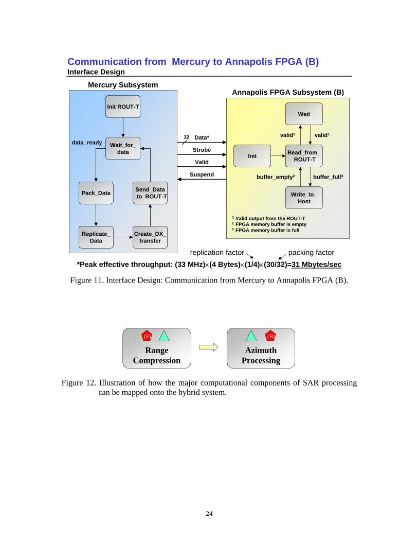
24
Read_from_ROUT-T
Write_to_Host
Wait
buffer_empty2 buffer_full3
valid1 valid1
Init
1 Valid output from the ROUT-T2 FPGA memory buffer is empty 3 FPGA memory buffer is full
Annapolis FPGA Subsystem (B)
32 Data*
Strobe
Valid
Suspend
Mercury Subsystem
Init ROUT-T
Wait_for_data
Pack_Data
Create_DX_transfer
data_ready
Replicate_Data
Send_Data_to_ROUT-T
Communication from Mercury to Annapolis FPGA (B)Interface Design
*Peak effective throughput: (33 MHz)×(4 Bytes)×(1/4)×(30/32)=31 Mbytes/secreplication factor packing factor
Figure 11. Interface Design: Communication from Mercury to Annapolis FPGA (B).
RangeCompression
(F)
AzimuthProcessing
(B)
Figure 12. Illustration of how the major computational components of SAR processing can be mapped onto the hybrid system.
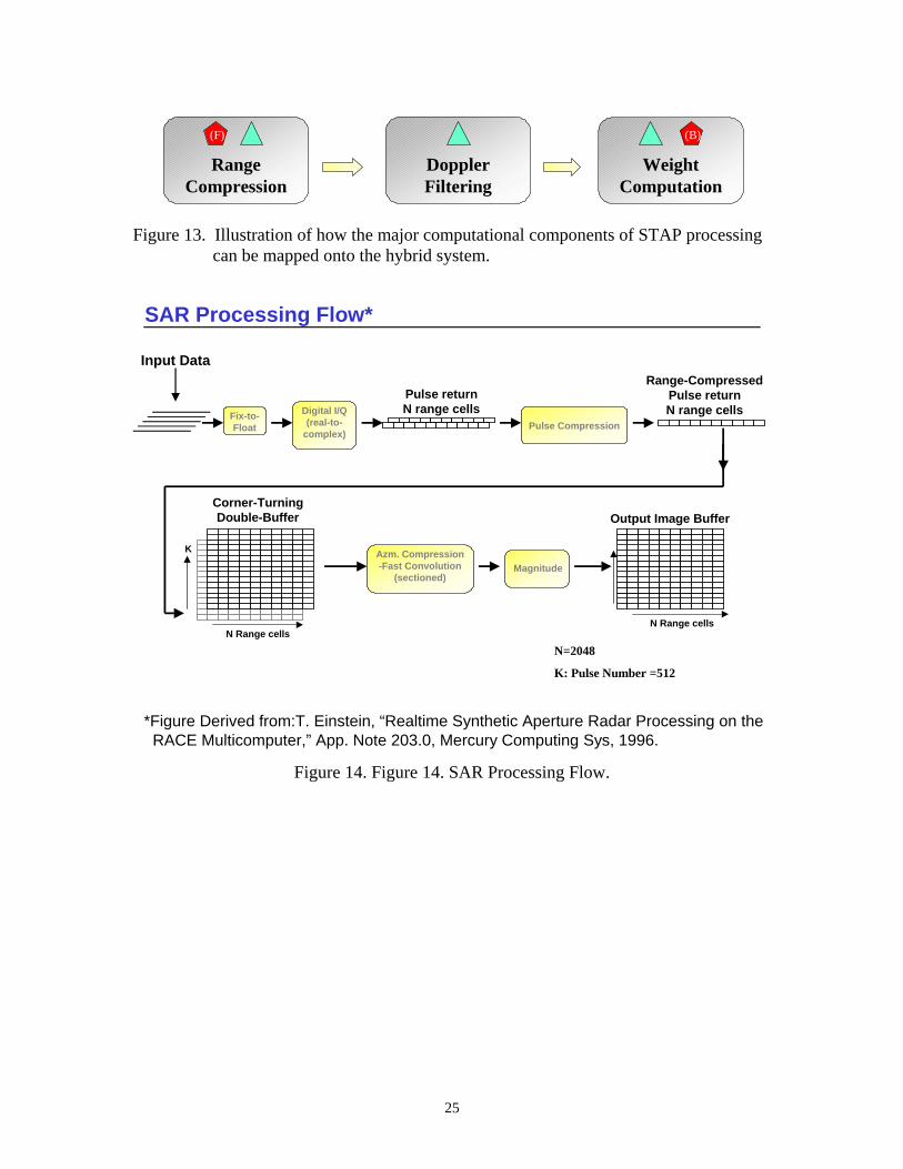
25
RangeCompression
DopplerFiltering
WeightComputation
(F) (B)
Figure 13. Illustration of how the major computational components of STAP processing can be mapped onto the hybrid system.
Pulse CompressionFix-to-Float
Input Data
Digital I/Q (real-to-
complex)
Pulse returnN range cells
Range-Compressed Pulse returnN range cells
MagnitudeAzm. Compression-Fast Convolution
(sectioned)
Output Image Buffer
N Range cells
K
Corner-TurningDouble-Buffer
N Range cells
N=2048
K: Pulse Number =512
SAR Processing Flow*
*Figure Derived from:T. Einstein, “Realtime Synthetic Aperture Radar Processing on the RACE Multicomputer,” App. Note 203.0, Mercury Computing Sys, 1996.
Figure 14. Figure 14. SAR Processing Flow.
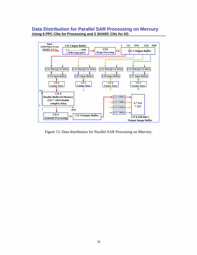
26
2048153610245121CN 2 Input Buffer
512
1
1, 2, ……, …… 2048( 2048 range gates)
Input(Odd Pulses From
SHARC CN 1) CN2Range Processing
CN2 DMA CN3 DMA
CN5 Input Buffer
CN 5Corner Turn
CN 4Double-Buffered Memory
(512 * 1024 double complex data)
1
CN2 DMA CN3 DMA
CN4 Input Buffer
CN 4Corner Turn
CN2 DMA CN3 DMA
CN6 Input Buffer
CN 6Corner Turn
CN2 DMA CN3 DMA
CN7 Input Buffer
CN 7Corner Turn
CN 4 Azimuth Processing
CN 4 Output Buffer CN 8 (SHARC)Output Image Buffer
CN 4 DMA
CN 5 DMA
CN 6 DMA
CN 7 DMA1024
4 * 512* 512
Data Distribution for Parallel SAR Processing on MercuryUsing 6 PPC CNs for Processing and 2 SHARC CNs for I/O
CN 2 Output Buffer
Figure 15. Data distribution for Parallel SAR Processing on Mercury.
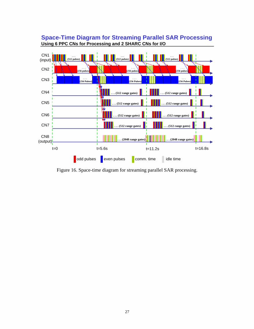
27
Space-Time Diagram for Streaming Parallel SAR ProcessingUsing 6 PPC CNs for Processing and 2 SHARC CNs for I/O
. . . (2048 range gates). . . (2048 range gates)
. . .(512 pulses)
. . . (512 range gates)
. . . (512 range gates)
. . . (512 range gates)
. . . (512 range gates)
. . .(512 pulses)
. . .(512 pulses)
. . .(256 pulses)
. . .(256 pulses)
. . .(256 pulses)
. . .(256 Pulses)
. . .(256 Pulses)
. . .(256 Pulses)
t=0
CN8(output)
CN7
CN6
CN5
CN4
CN3
CN2
CN1(input)
odd pulses comm. timeeven pulses
. . . (512 range gates) . . . (512 range gates)
. . . (512 range gates) . . . (512 range gates)
idle time
t=16.8st=11.2st=5.6s
Figure 16. Space-time diagram for streaming parallel SAR processing.
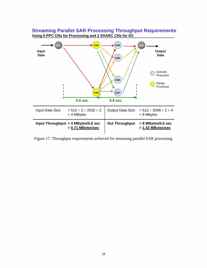
28
CN1 CN2
CN3
CN5
CN6
CN8
CN7
CN4
InputData
OutputData
Streaming Parallel SAR Processing Throughput RequirementsUsing 6 PPC CNs for Processing and 2 SHARC CNs for I/O
RangeProcessor
AzimuthProcessor
5.6 sec 5.6 sec
Input Data Size = 512 × 2 × 2032 × 2= 4 MBytes
Input Throughput = 4 MBytes/5.6 sec= 0.71 MBytes/sec
Output Data Size = 512 × 2048 × 2 × 4 = 8 Mbytes
Out Throughput = 8 MBytes/5.6 sec= 1.42 MBytes/sec
Figure 17. Throughput requirements achieved for streaming parallel SAR processing.
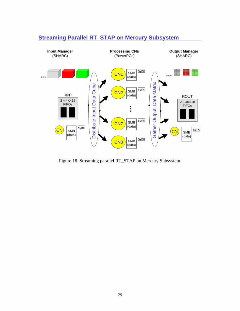
29
Processing CNs(PowerPCs)
2 – 4K×18FIFOs
ROUT
Output Manager(SHARC)
CN SMB(data)
sync
2 – 4K×18FIFOs
RINT
Input Manager(SHARC)
CN SMB(data)
sync
SMB(data)
syncCN1
SMB(data)
syncCN2
SMB(data)
syncCN8
SMB(data)
syncCN7
Streaming Parallel RT_STAP on Mercury Subsystem
Dis
tribu
te In
put D
ata
Cub
e
Gat
her O
utpu
t D
ata
Mat
rix
Figure 18. Streaming parallel RT_STAP on Mercury Subsystem.
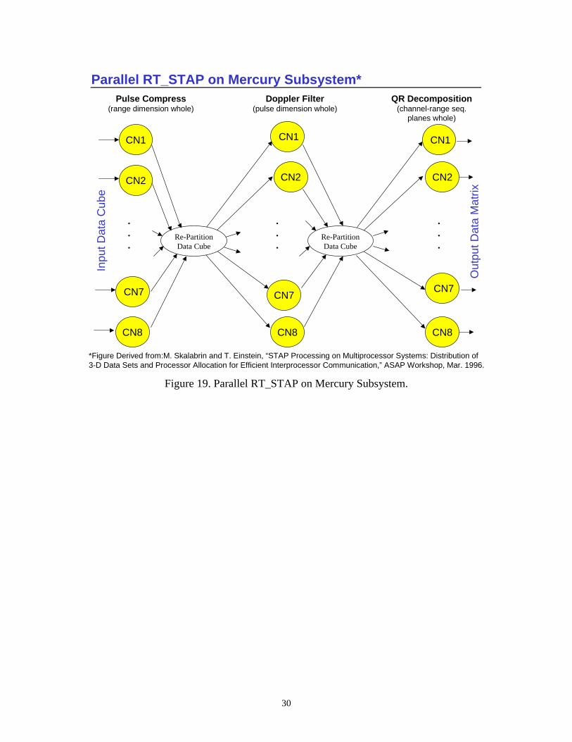
30
Pulse Compress(range dimension whole)
Doppler Filter(pulse dimension whole)
QR Decomposition(channel-range seq.
planes whole)
Re-PartitionData Cube
Re-PartitionData Cube
.
.
.
CN1
CN2
CN7
CN8
CN1
CN2
CN7
CN8
CN1
CN2
CN7
CN8
.
.
.
.
.
.
Inpu
t Dat
a C
ube
Out
put D
ata
Mat
rix
Parallel RT_STAP on Mercury Subsystem*
*Figure Derived from:M. Skalabrin and T. Einstein, “STAP Processing on Multiprocessor Systems: Distribution of 3-D Data Sets and Processor Allocation for Efficient Interprocessor Communication,” ASAP Workshop, Mar. 1996.
Figure 19. Parallel RT_STAP on Mercury Subsystem.
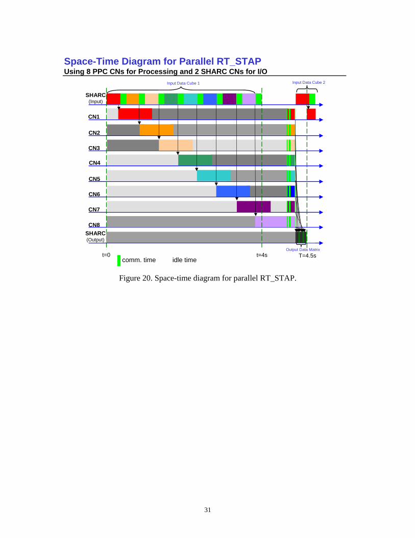
31
Space-Time Diagram for Parallel RT_STAP Using 8 PPC CNs for Processing and 2 SHARC CNs for I/O
CN4
CN7
CN8
CN2
CN5
CN6
SHARC(Output)
CN1
CN3
Input Data Cube 1
SHARC(Input)
comm. time idle timet=0 t=4s T=4.5s
Output Data Matrix
Input Data Cube 2
Figure 20. Space-time diagram for parallel RT_STAP.
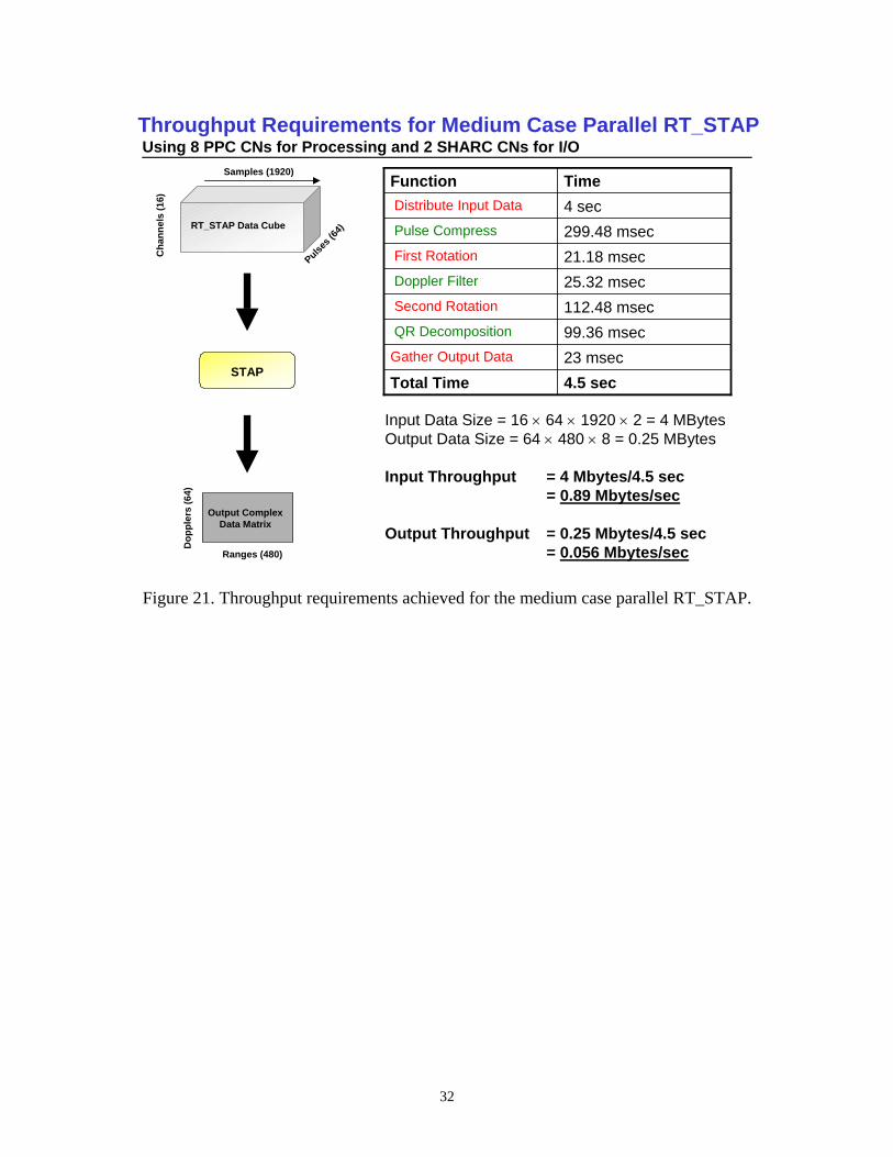
32
RT_STAP Data Cube
Cha
nnel
s (1
6)
Pulses (
64)
Samples (1920)
STAP
Dop
pler
s (6
4)
Ranges (480)
Output ComplexData Matrix
23 msecGather Output Data
4 secDistribute Input Data
4.5 secTotal Time
99.36 msecQR Decomposition112.48 msecSecond Rotation25.32 msecDoppler Filter21.18 msecFirst Rotation299.48 msecPulse Compress
TimeFunction
Input Data Size = 16 × 64 × 1920 × 2 = 4 MBytes Output Data Size = 64 × 480 × 8 = 0.25 MBytes
Input Throughput = 4 Mbytes/4.5 sec = 0.89 Mbytes/sec
Output Throughput = 0.25 Mbytes/4.5 sec= 0.056 Mbytes/sec
Throughput Requirements for Medium Case Parallel RT_STAP Using 8 PPC CNs for Processing and 2 SHARC CNs for I/O
Figure 21. Throughput requirements achieved for the medium case parallel RT_STAP.
33
Conclusion
Technology Transfer
Technology transfer took place along five main paths: (1) the DARPA Adapted Computing Systems (ACS) community through PI (Principal Investigator) meetings and other conferences (plus communications with PIs and program managers in related areas); (2) the employees and technical support contacts at Mercury Computer Systems, Inc.; (3) the employees and technical support contacts at Annapolis Micro Systems, Inc.; (4) contacts with various defense contractors such as Northrop Grumman; and (5) the academic high-performance embedded computing research community.
Regarding path (1), we worked with DARPA and other PIs associated with related projects to ensure efficient transfer of information and technology. We attended all PI meetings and helped support DARPA in presenting the results of this effort for further program funding.
For paths (2) and (3), we consulted with the vendors on a regular basis, especially during the period of time in which the prototype system was being constructed. We kept both vendors informed on the current status of the prototype throughout the project. The success of our project sparked interaction between the two vendors in terms of defining and refining interface standards for interconnecting their products. These new standards, which were not available at the time we were constructing our prototype, make it much easier to construct an FPGA/DSP/GPP system such as the one implemented for this project.
The transfer along path (4) was important because it enabled our proposed approaches to be considered and evaluated by defense systems designers and end-users. Also, staying in close contact with major defense contractors and other contractors that were part of the ACS program, ensured that the approaches and systems we developed were realistic.
As indicated by path (5), it was important to keep the academic research community informed about our developments. The publications that resulted from this project have made an impact and serve to illustrate the types of research of interest to DARPA. It also illustrated that there is an abundance of basic, fundamental research to be done on the way to solving important problems of military interest.
Deliverables
This project delivered an abundance of results of both practical and theoretical importance. Many of these results have been published as journal and conference papers, and copies of these papers are provided in the appendices of this report. Online links to delivered publications, presentation materials, dissertations, theses, and additional materials are provided in the References and Additional Materials sections of the report. Associated with each publication is one or more tool or technique of immediate practical importance to practitioners in the area of embedded high-performance systems design and implementation. Also delivered was a prototype platform in which the three technologies of interest (FPGA, DSP, and GPP) were integrated into a single high-performance computational engine. This platform served as a test bed in which

34
experimental tests, evaluations, and assessments associated with the research were conducted.
The theme of the project was to focus on techniques and systems for minimizing power consumption requirements for two particular radar-processing applications. In addition to providing results along these lines, many of the techniques and results delivered are applicable to a much broader set of problems that arise in high-performance, SWAP-constrained embedded systems.
35
References
[1A] Jeffrey T. Muehring and John K. Antonio, “Optimal Configuration of an Embedded Parallel System for Synthetic Aperture Radar Processing,” Proceedings of the International Conference on Signal Processing Applications & Technology, Boston, MA, Oct. 1996, pp. 1489-1494.
Location: Appendix A and http://www.cs.ou.edu/~antonio/pubs/conf033.pdf
[2B] Jeffrey T. Muehring and John K. Antonio, “Optimal Configuration of Compute Nodes for Synthetic Aperture Radar Processing,” Proceedings of the International Workshop on Embedded HPC Systems and Applications (EHPC ‘98), in Lecture Notes in Computer Science 1388: Parallel and Distributed Processing, edited by Jose Rolim, sponsor: IEEE Computer Society, Orlando, FL, USA, Apr. 1998, pp. 987-993.
Location: Appendix B and http://www.cs.ou.edu/~antonio/pubs/conf035.pdf Presentation Materials: http://www.cs.ou.edu/~antonio/pubs/p-conf035.pdf
[3] Jeffrey T. Muehring, Optimal Configuration of a Parallel Embedded System for Synthetic Aperture Radar Processing, Master’s Thesis, Department of Computer Science, Texas Tech University, Lubbock, TX, Dec. 1997.
Location: http://www.cs.ou.edu/~antonio/pubs/muehring_thesis.pdf
[4C] Jack M. West and John K. Antonio, “Simulation of the Communication Time for a Space-Time Adaptive Processing Algorithm on a Parallel Embedded System,” Proceedings of the International Workshop on Embedded HPC Systems and Applications (EHPC ‘98), in Lecture Notes in Computer Science 1388: Parallel and Distributed Processing, edited by Jose Rolim, sponsor: IEEE Computer Society, Orlando, FL, USA, Apr. 1998, pp. 979-986.
Location: Appendix C and http://www.cs.ou.edu/~antonio/pubs/conf036.pdf Presentation Materials: http://www.cs.ou.edu/~antonio/pubs/p-conf036.pdf
[5D] Jack M. West and John K. Antonio, “A Genetic Algorithm Approach to Scheduling Communications for a Class of Parallel Space-Time Adaptive Processing Algorithms,” Proceedings of the 5th International Workshop on Embedded/Distributed HPC Systems and Applications (EHPC 2000), in Lecture Notes in Computer Science, IPDPS 2000 Workshops, sponsor: IEEE Computer Society, Cancun, Mexico, May 2000, pp. 855-861.
Location: Appendix D and http://www.cs.ou.edu/~antonio/pubs/conf042.pdf Presentation Materials: http://www.cs.ou.edu/~antonio/pubs/p-conf042.pdf
[6E] Jack M. West and John K. Antonio, “A Genetic-Algorithm Approach to Scheduling Communications for Embedded Parallel Space-Time Adaptive Processing Algorithms,” Journal of Parallel and Distributed Computing, Vol. 62, No. 9, Sept. 2002, pp. 1386-1406. Location: Appendix E and http://www.cs.ou.edu/~antonio/pubs/jour016.pdf
36
[7] Jack M. West, Simulation of Communication Time for a Space-Time Adaptive Processing Algorithm on a Parallel Embedded System, Master’s Thesis, Department of Computer Science, Texas Tech University, Lubbock, TX, Aug. 1998.
Location: http://www.cs.ou.edu/~antonio/pubs/west_thesis.pdf
[8] Jack M. West, Processor Allocation, Message Scheduling, and Algorithm Selection for Space-Time Adaptive Processing, Doctoral Dissertation, Department of Computer Science, Texas Tech University, Lubbock, TX, Aug. 2000.
Location: http://www.cs.ou.edu/~antonio/pubs/west_diss.pdf
[9F] Timothy Osmulski, Jeffrey T. Muehring, Brian Veale, Jack M. West, Hongping Li, Sirirut Vanichayobon, Seok-Hyun Ko, John K. Antonio, and Sudarshan K. Dhall, “A Probabilistic Power Prediction Tool for the Xilinx 4000-Series FPGA,” Proceedings of the 5th International Workshop on Embedded/Distributed HPC Systems and Applications (EHPC 2000), in Lecture Notes in Computer Science, IPDPS 2000 Workshops, sponsor: IEEE Computer Society, Cancun, Mexico, May 2000, pp. 776-783.
Location Appendix F and http://www.cs.ou.edu/~antonio/pubs/conf041.pdf Presentation Materials: http://www.cs.ou.edu/~antonio/pubs/p-conf041.pdf
[10] Timothy A. Osmulski, Implementation and Evaluation of a Power Prediction Model for a Field Programmable Gate Array, Master’s Thesis, Department of Computer Science, Texas Tech University, Lubbock, TX, May 1998.
Location: http://www.cs.ou.edu/~antonio/pubs/osmulski_thesis.pdf
[11G] Hongping Li, John K. Antonio, and Sudarshan K. Dhall, “Fast and Precise Power Prediction for Combinational Circuits,” Proceedings of the IEEE Symposium on VLSI, sponsor: IEEE, Tampa, FL, Feb 2003, pp. 254-259.
Location Appendix G and http://www.cs.ou.edu/~antonio/pubs/conf046.pdf Presentation Materials: http://www.cs.ou.edu/~antonio/pubs/p-conf046.pdf
[12H] Nikhil D. Gupta, John K. Antonio, and Jack M. West, “Reconfigurable Computing for Space-Time Adaptive Processing” Proceedings of the Sixth Annual IEEE Symposium on Field Programmable Custom Computing Machines (FCCM), Napa, CA, USA, Apr. 1998, pp. 335-336.
Location: Appendix H and http://www.cs.ou.edu/~antonio/pubs/conf037.pdf
[13] Nikhil D. Gupta, Reconfigurable Computing for Space-Time Adaptive Processing, Master’s Thesis, Department of Computer Science, Texas Tech University, Lubbock, TX, August 1998.
Location: http://www.cs.ou.edu/~antonio/pubs/gupta_thesis.pdf
[14] Brian F. Veale, Study of Power Consumption For High-Performance Reconfigurable Computing Architectures, Master’s Thesis, Department of Computer Science, Texas Tech University, Lubbock, TX, August 1999.
Location: http://www.cs.ou.edu/~antonio/pubs/veale_thesis.pdf
37
[15I] Jeffrey T. Muehring and John K. Antonio, “Minimizing Power Consumption using Signal Activity Transformations for Very Deep FPGA Pipelines,” Proceedings of the Military and Aerospace Applications for Programmable Devices and Technologies Conference (MAPLD 2000), sponsors: NASA and Johns Hopkins University/Applied Physics Laboratory, Laurel, MD, Sep. 2000.
Location Appendix I and http://www.cs.ou.edu/~antonio/pubs/conf044.pdf Presentation Materials: http://www.cs.ou.edu/~antonio/pubs/p-conf044.pdf
[16J] S. Vanichayobon, Sudarshan K. Dhall, S. Lakshmivarahan, and John K. Antonio, “Power-speed Trade-off in Parallel Prefix Circuits,” Proceedings of ITComm 2002, High-Performance Pervasive Computing Conference, sponsor: SPIE, Boston, MA, July/Aug. 2002, pp. 109-120.
Location Appendix J and http://www.cs.ou.edu/~antonio/pubs/conf045.pdf Presentation Materials: http://www.cs.ou.edu/~antonio/pubs/p-conf045.pdf
[17] Sirirut Vanichayobon, Power-Speed Trade-Off in Parallel Prefix Circuits, Doctoral Dissertation, School of Computer Science, University of Oklahoma, Norman, OK, 2002.
Location: http://www.cs.ou.edu/~antonio/pubs/sirirut_diss.pdf
[18K] Jack M. West, Hongping Li, Sirirut Vanichayobon, Jeffrey T. Muehring, John K. Antonio, and Sudarshan K. Dhall, “A Hybrid FPGA/DSP/GPP Prototype Architecture for SAR and STAP,” Proceedings of the Fourth Annual High Performance Embedded Computing Workshop, sponsors: U.S. Navy and Defense Advanced Research Projects Agency (DARPA), MIT Lincoln Laboratory Publications, Group 18, Lexington, MA, Sep. 2000, pp. 29-30.
Location: Appendix K and http://www.cs.ou.edu/~antonio/pubs/conf043.pdf Presentation Materials: http://www.cs.ou.edu/~antonio/pubs/p-conf043.pdf
38
Additional Materials
Annual Reviews and Kickoff Presented to DARPA
Fall 1999 Annual Review: http://www.cs.ou.edu/~antonio/pubs/p-ann_rev99acs.pdf Fall 1998 Annual Review: http://www.cs.ou.edu/~antonio/pubs/p-ann_rev98acs.pdf Fall 1997 Kickoff: http://www.cs.ou.edu/~antonio/pubs/p-kickoff97acs.pdf PI Meeting Presentations and Posters
Presentation, Spring 2000 PI Meeting: http://www.cs.ou.edu/~antonio/pubs/p-sp00acs.pdf Poster, Spring 2000 PI Meeting: http://www.cs.ou.edu/~antonio/pubs/poster-sp00acs.ppt
Presentation, Fall 1999 PI Meeting: http://www.cs.ou.edu/~antonio/pubs/p-fall99acs.pdf Poster, Fall 1999 PI Meeting: http://www.cs.ou.edu/~antonio/pubs/poster-fall99acs.ppt
Poster, Spring 1999 PI Meeting: http://www.cs.ou.edu/~antonio/pubs/poster-sp99acs.ppt
Poster, Fall 1998 PI Meeting: http://www.cs.ou.edu/~antonio/pubs/poster-fall98acs.ppt
Poster 1, Spring 1998 PI Meeting: http://www.cs.ou.edu/~antonio/pubs/poster1-sp98acs.ppt
Poster 2, Spring 1998 PI Meeting: http://www.cs.ou.edu/~antonio/pubs/poster2-sp98acs.ppt
Presentation, Fall 1997 PI Meeting: http://www.cs.ou.edu/~antonio/pubs/p-fall97acs.pdf Poster, Fall 1997 PI Meeting: http://www.cs.ou.edu/~antonio/pubs/poster-fall97acs.pdf Technical Report
Hongping Li, John K. Antonio, and Sudarshan K. Dhall, “Fast and Precise Power Prediction for Combinational Circuits,” University of Oklahoma, School of Computer Science, Technical Report No. CS-TR-02-001, Nov. 2002, 42 pages. http://www.cs.ou.edu/~antonio/pubs/tr013.pdf (expanded content of [11G]).
39
List of Acronyms
ACS Adaptive Computing Systems ASIC application specific integrated circuit CE compute element CLB configurable logic block CN compute node COTS commercial off the shelf DARPA Defense Advanced Research Projects Agency DSP digital signal processor FLOP floating-point operation FPGA field programmable gate array GA genetic algorithm GPP general-purpose processor IEEE Institute of Electrical and Electronics Engineers MIT Massachusetts Institute of Technology PC personal computer PCI peripheral component interconnection PI principal investigator RASSP rapid prototyping of application specific signal processors RT_STAP real-time space-time adaptive processing SAR synthetic aperture radar SHARC® “super” Harvard architecture STAP space-time adaptive processing SWAP size, weight, and power UAV unmanned aerial vehicle
40
Appendix A: Jeffrey T. Muehring and John K. Antonio, “Optimal Configuration of an Embedded Parallel System for Synthetic Aperture Radar Processing,” Proceedings of the International Conference on Signal Processing Applications & Technology, Boston, MA, Oct. 1996, pp. 1489-1494.
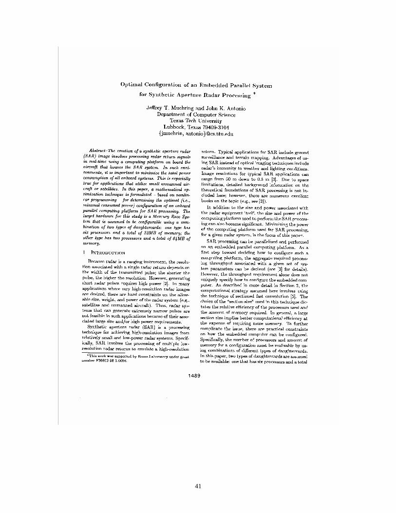
41
42
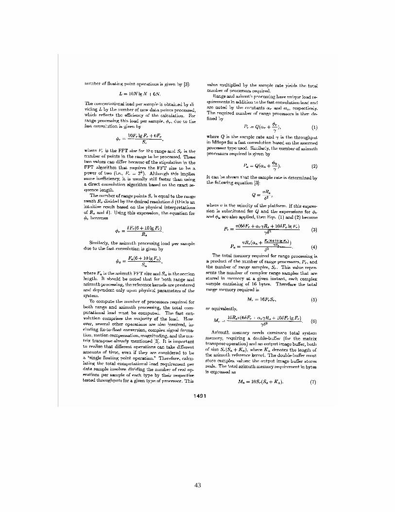
43
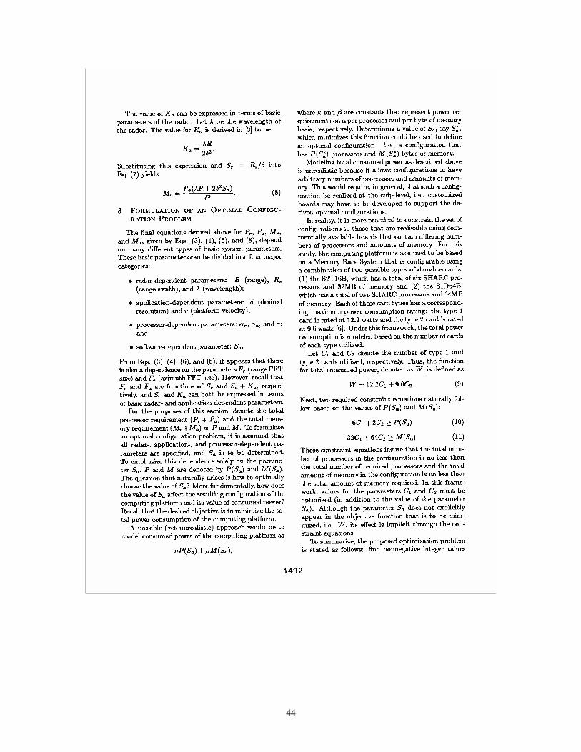
44
45
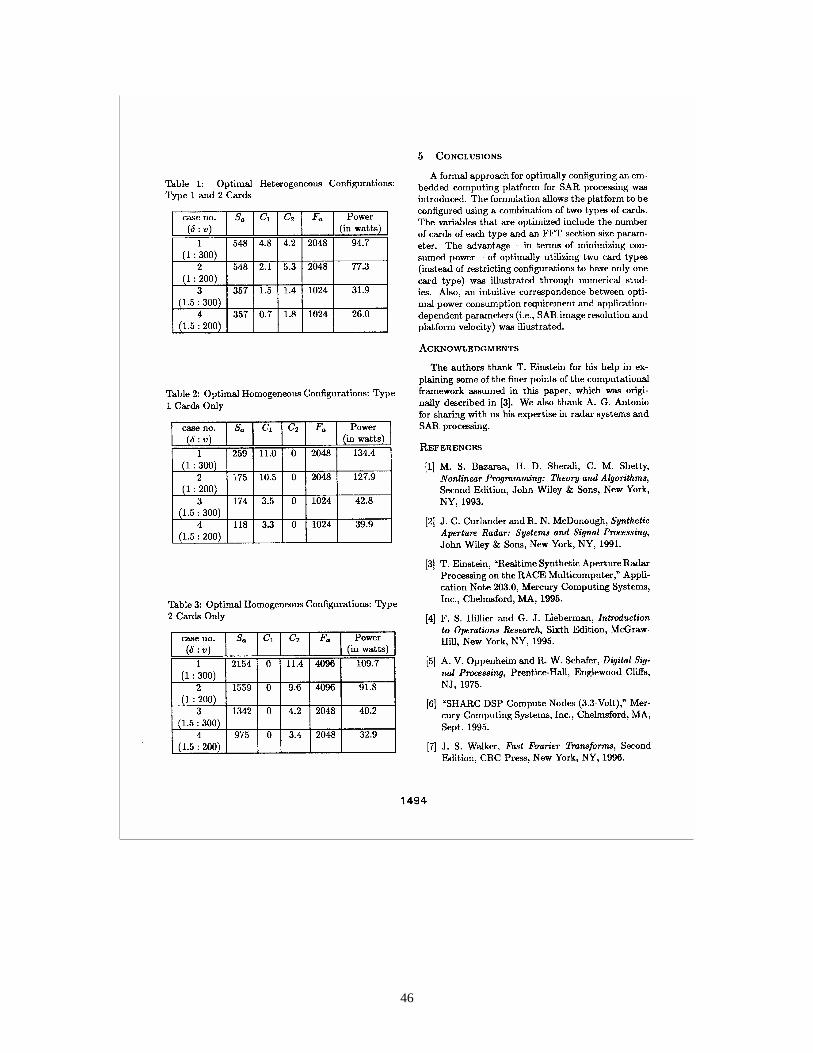
46
47
Appendix B: Jeffrey T. Muehring and John K. Antonio, “Optimal Configuration of Compute Nodes for Synthetic Aperture Radar Processing,” Proceedings of the International Workshop on Embedded HPC Systems and Applications (EHPC ‘98), in Lecture Notes in Computer Science 1388: Parallel and Distributed Processing, edited by Jose Rolim, sponsor: IEEE Computer Society, Orlando, FL, USA, Apr. 1998, pp. 987-993.
48
49
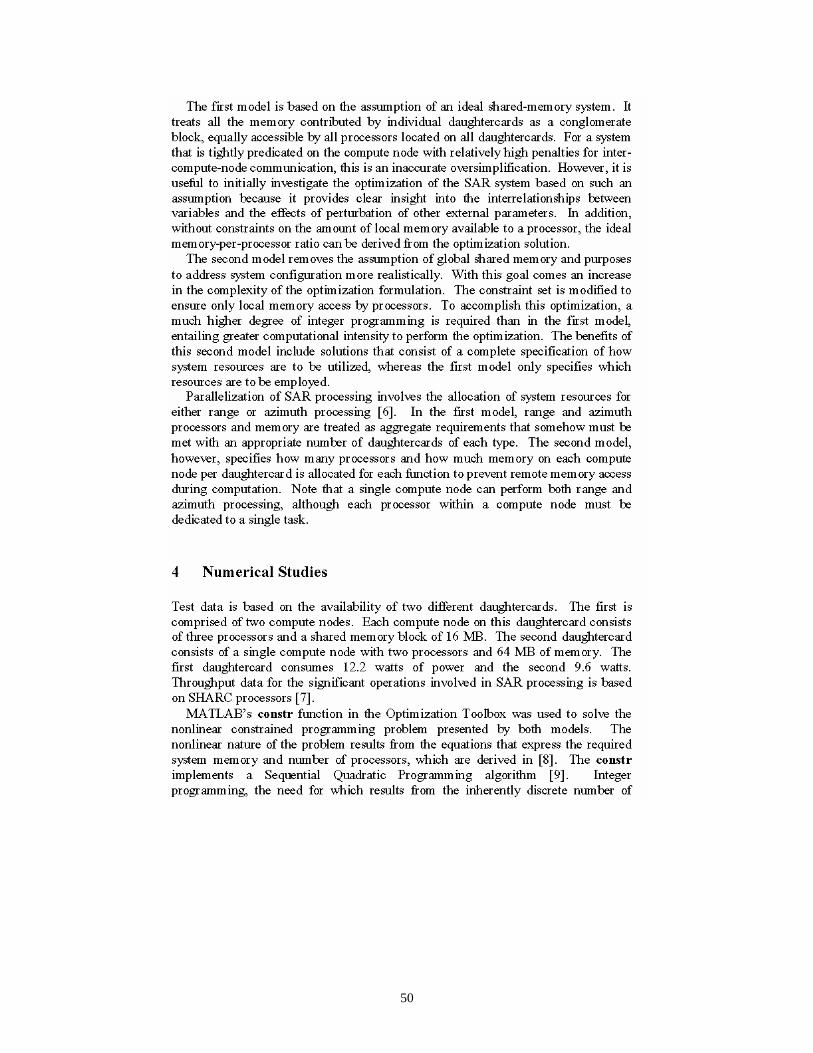
50
51
52
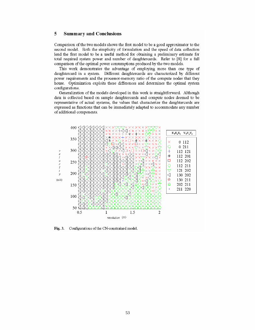
53
54
55
Appendix C: Jack M. West and John K. Antonio, “Simulation of the Communication Time for a Space-Time Adaptive Processing Algorithm on a Parallel Embedded System,” Proceedings of the International Workshop on Embedded HPC Systems and Applications (EHPC ‘98), in Lecture Notes in Computer Science 1388: Parallel and Distributed Processing, edited by Jose Rolim, sponsor: IEEE Computer Society, Orlando, FL, USA, Apr. 1998, pp. 979-986.
56
57
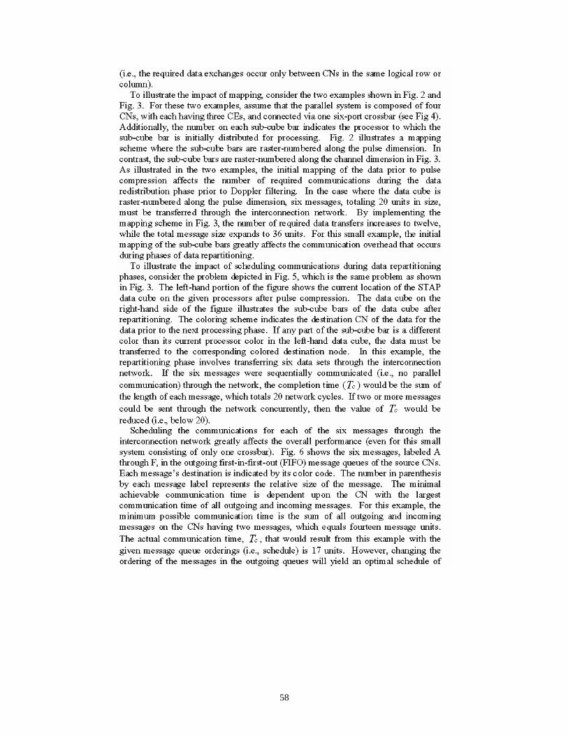
58
59
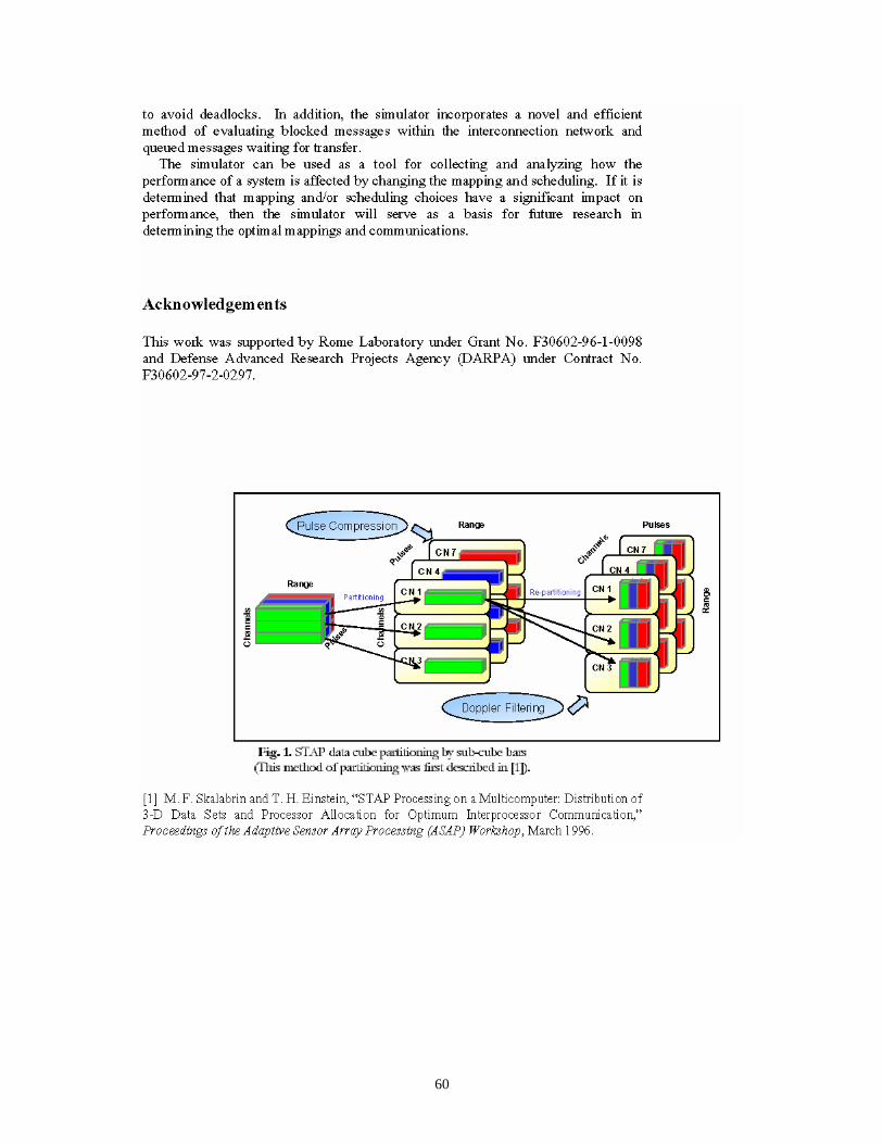
60
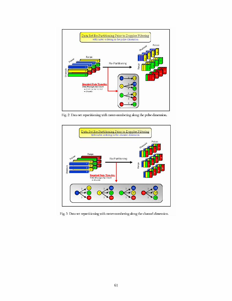
61
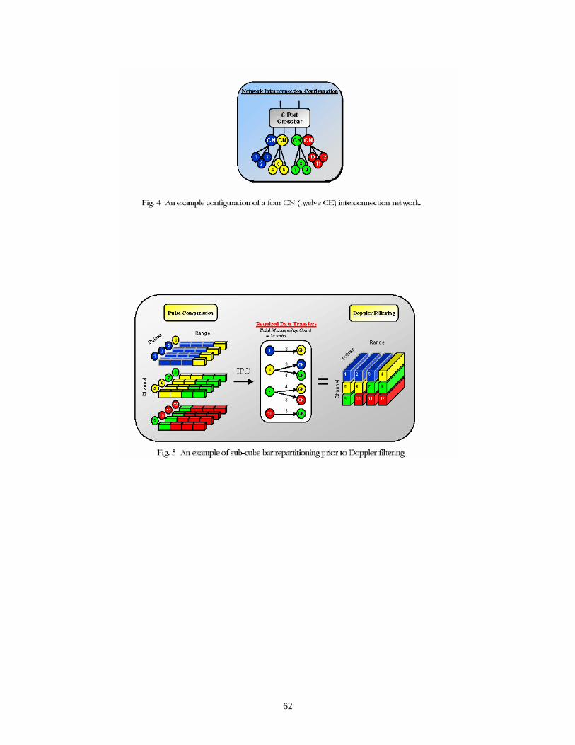
62
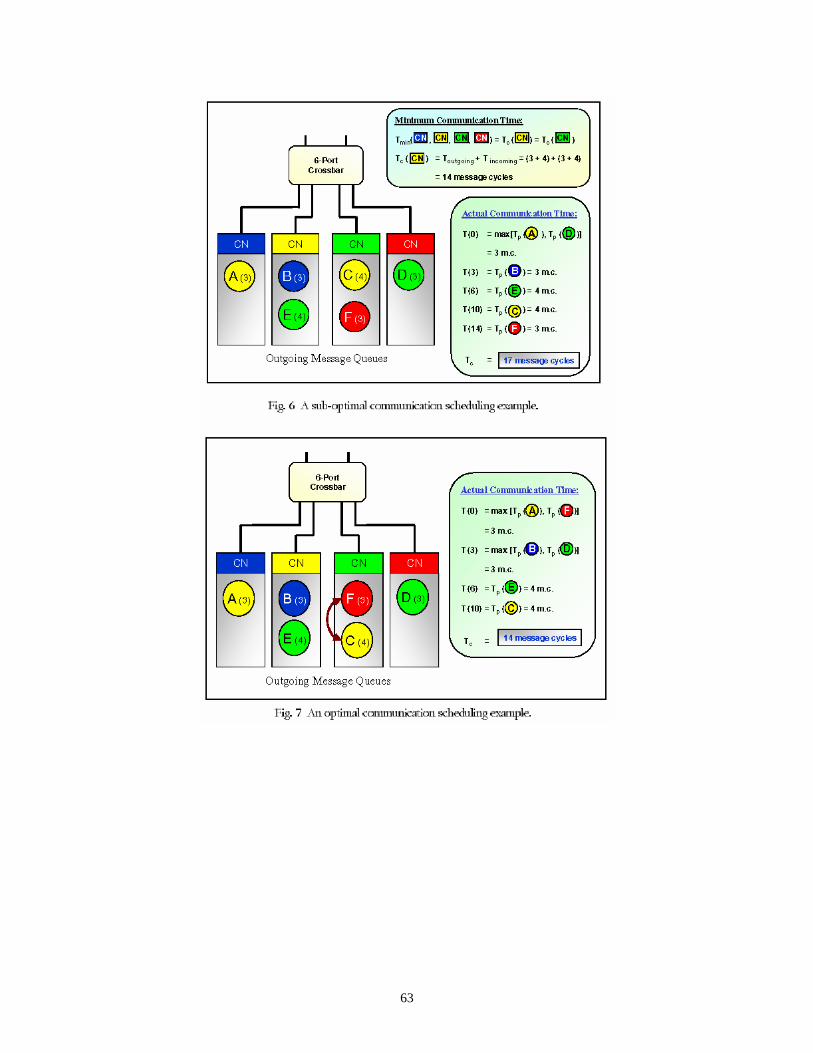
63
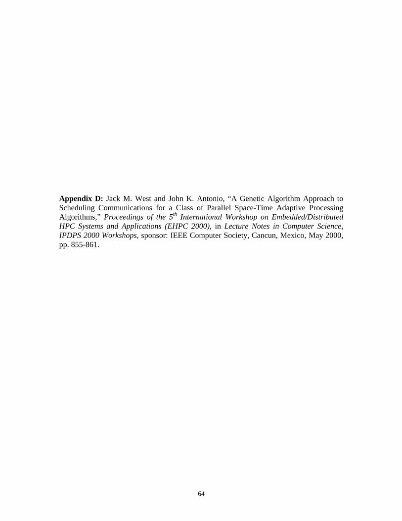
64
Appendix D: Jack M. West and John K. Antonio, “A Genetic Algorithm Approach to Scheduling Communications for a Class of Parallel Space-Time Adaptive Processing Algorithms,” Proceedings of the 5th International Workshop on Embedded/Distributed HPC Systems and Applications (EHPC 2000), in Lecture Notes in Computer Science, IPDPS 2000 Workshops, sponsor: IEEE Computer Society, Cancun, Mexico, May 2000, pp. 855-861.
65
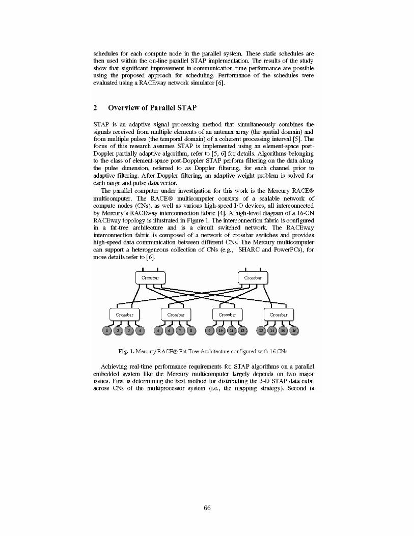
66
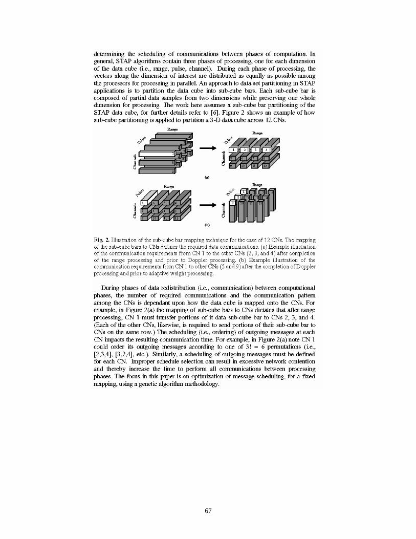
67
68
69
70
71
72
Appendix E: Jack M. West and John K. Antonio, “A Genetic-Algorithm Approach to Scheduling Communications for Embedded Parallel Space-Time Adaptive Processing Algorithms,” Journal of Parallel and Distributed Computing, Vol. 62, No. 9, Sept. 2002, pp. 1386-1406.
73
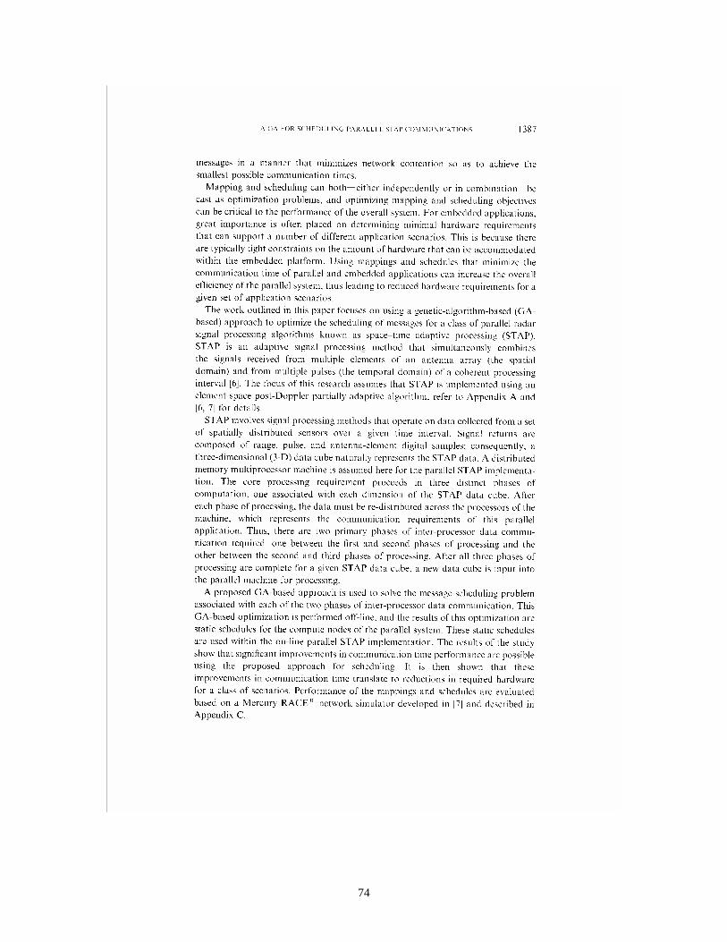
74
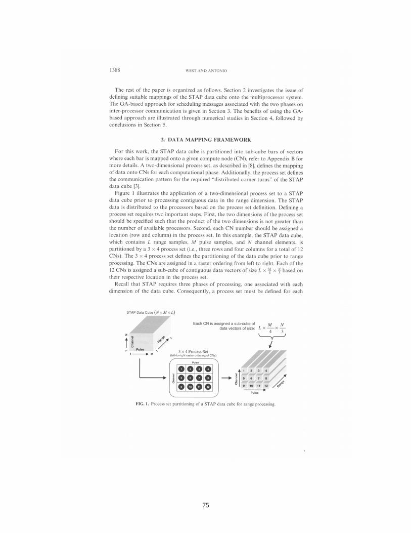
75
76
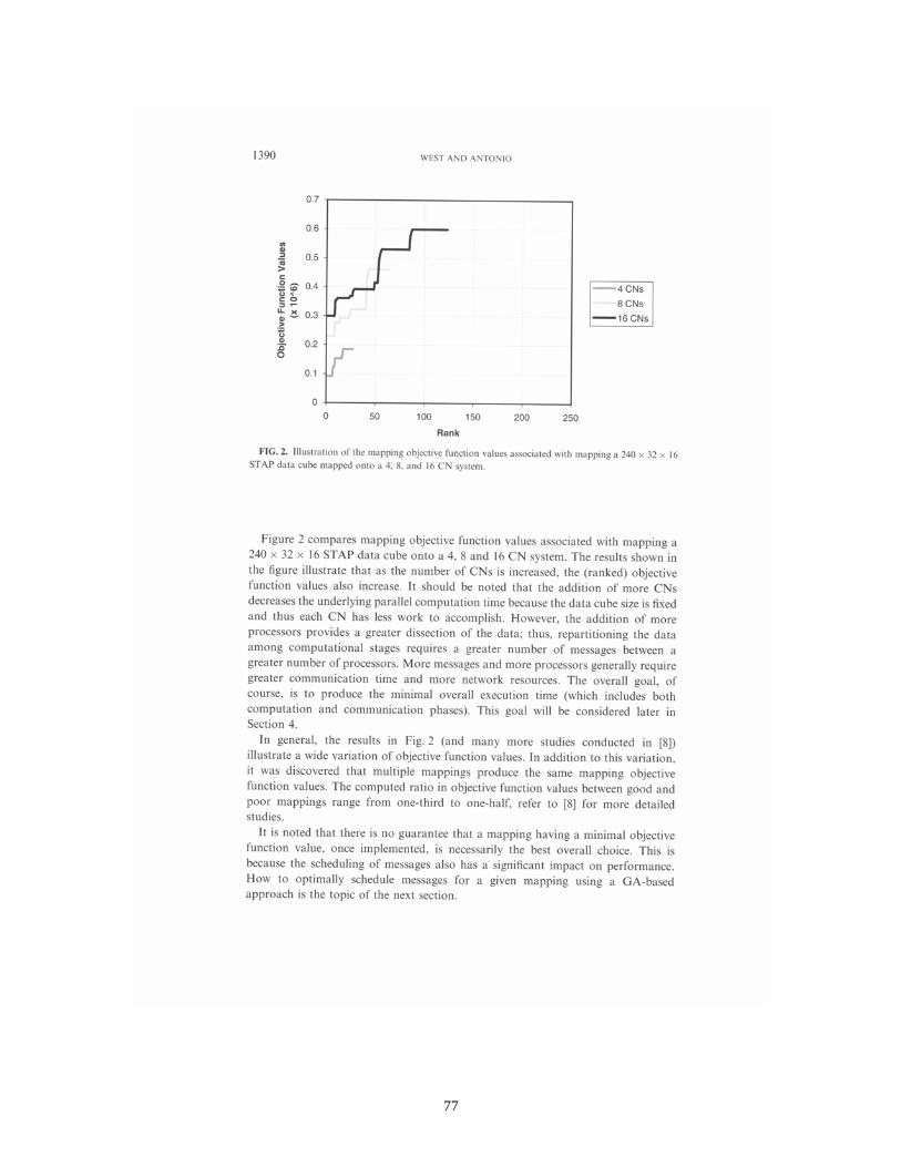
77
78
79
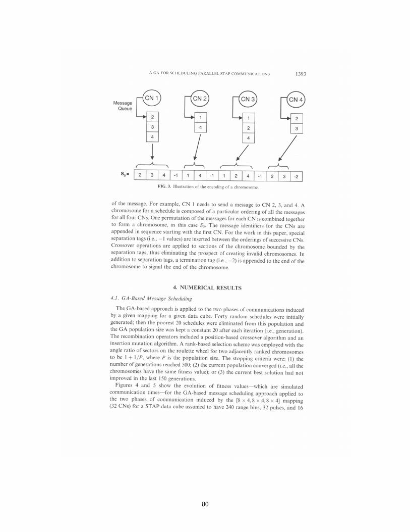
80
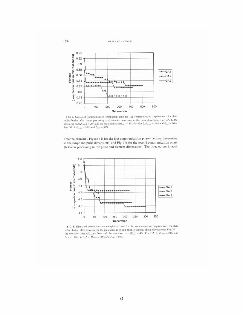
81
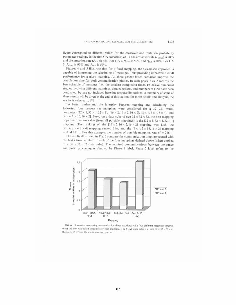
82
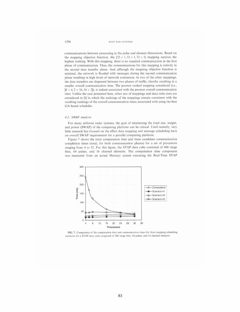
83
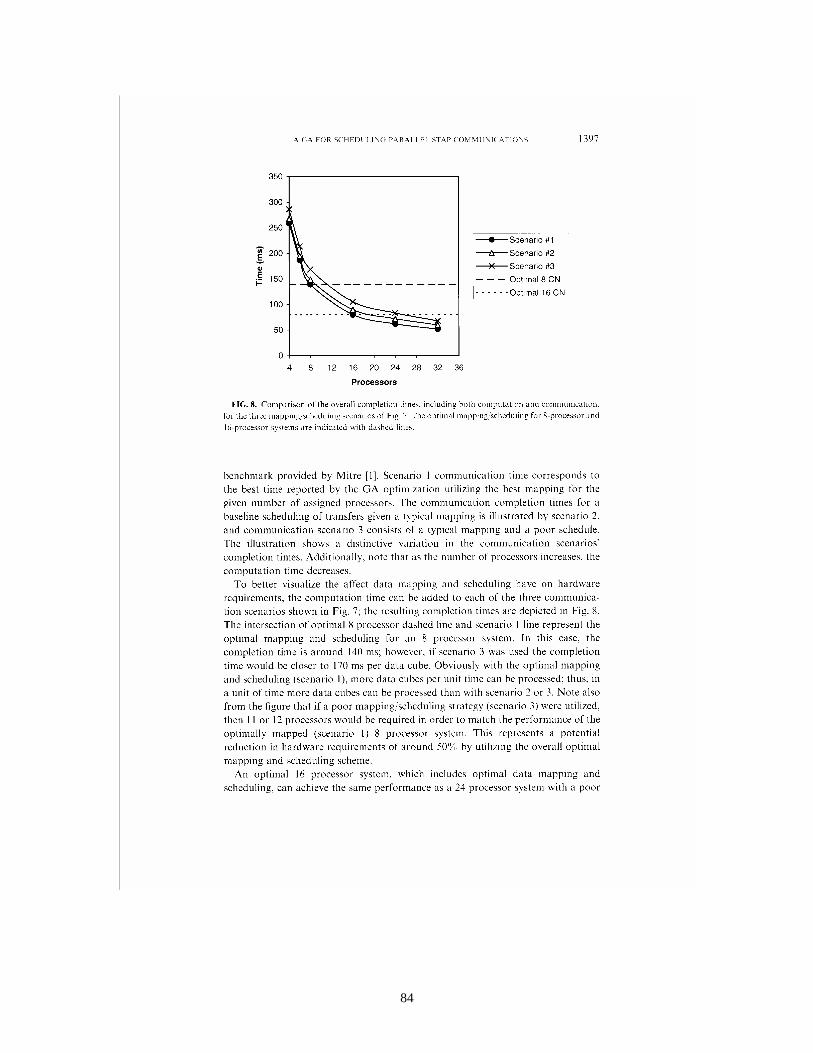
84
85
86
87
88
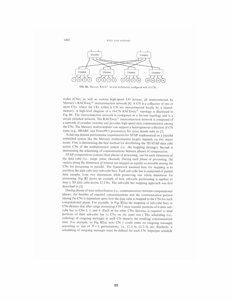
89
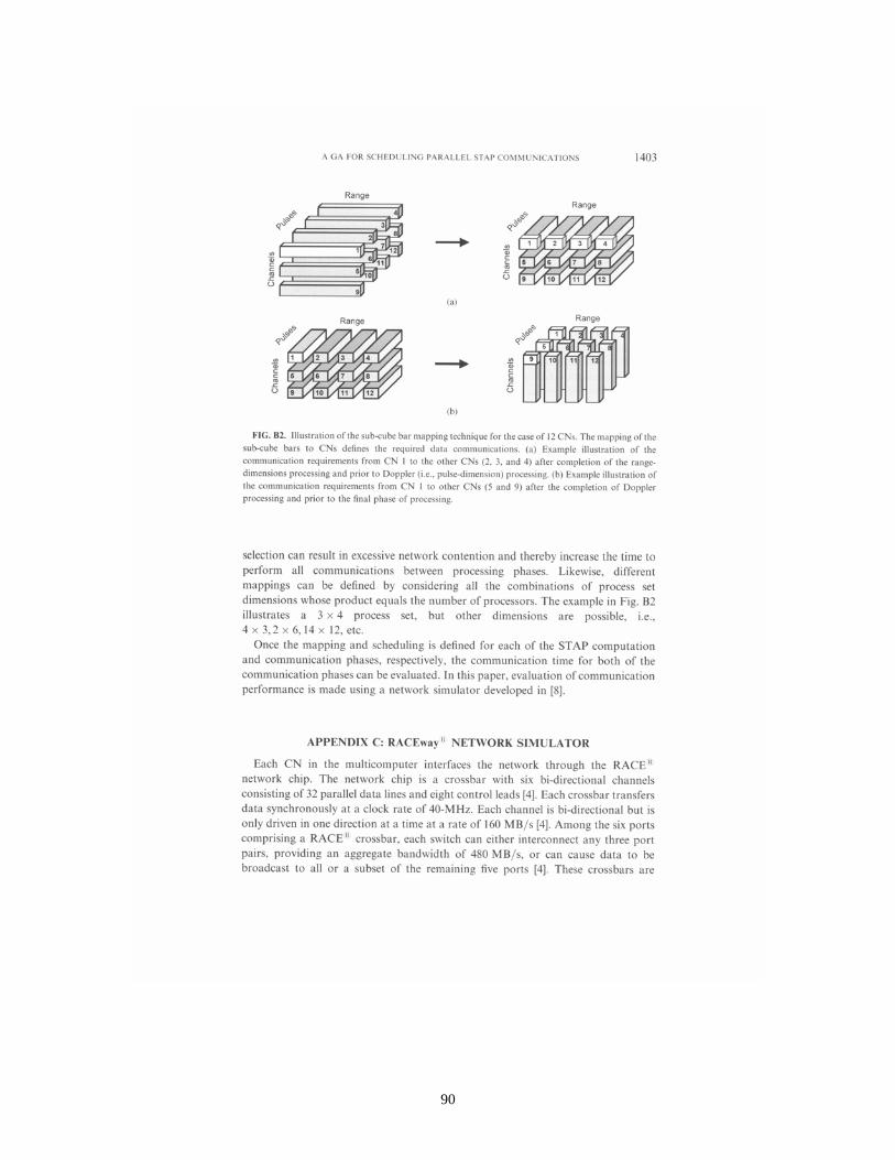
90
91
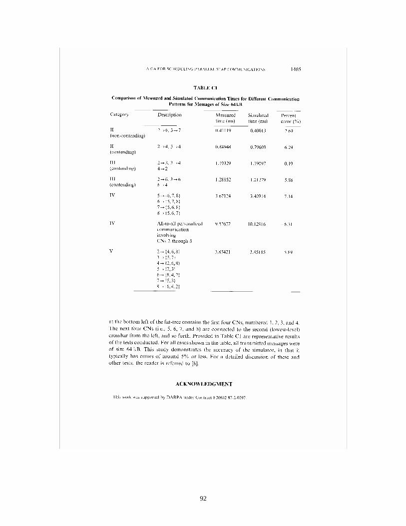
92
93
94
Appendix F: Timothy Osmulski, Jeffrey T. Muehring, Brian Veale, Jack M. West, Hongping Li, Sirirut Vanichayobon, Seok-Hyun Ko, John K. Antonio, and Sudarshan K. Dhall, “A Probabilistic Power Prediction Tool for the Xilinx 4000-Series FPGA,” Proceedings of the 5th International Workshop on Embedded/Distributed HPC Systems and Applications (EHPC 2000), in Lecture Notes in Computer Science, IPDPS 2000 Workshops, sponsor: IEEE Computer Society, Cancun, Mexico, May 2000, pp. 776-783.
95
96
97
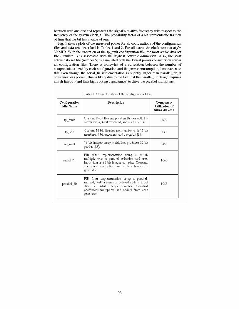
98
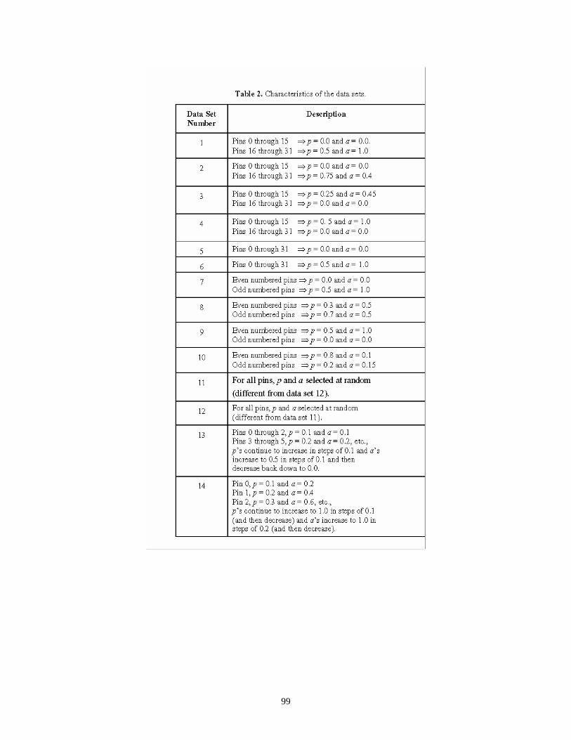
99
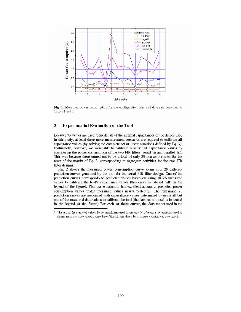
100
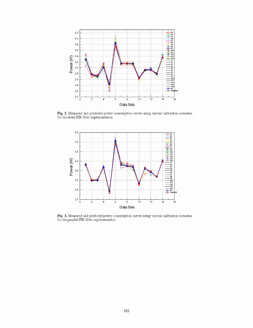
101
102
103
Appendix G: Hongping Li, John K. Antonio, and Sudarshan K. Dhall, “Fast and Precise Power Prediction for Combinational Circuits,” Proceedings of the IEEE Symposium on VLSI, sponsor: IEEE, Tampa, FL, Feb 2003, pp. 254-259.
104
105
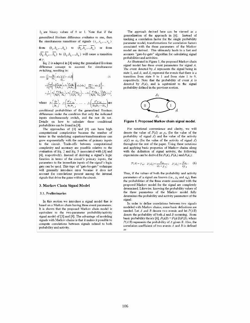
106
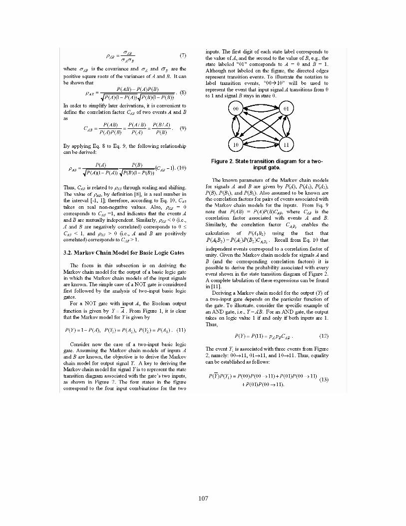
107
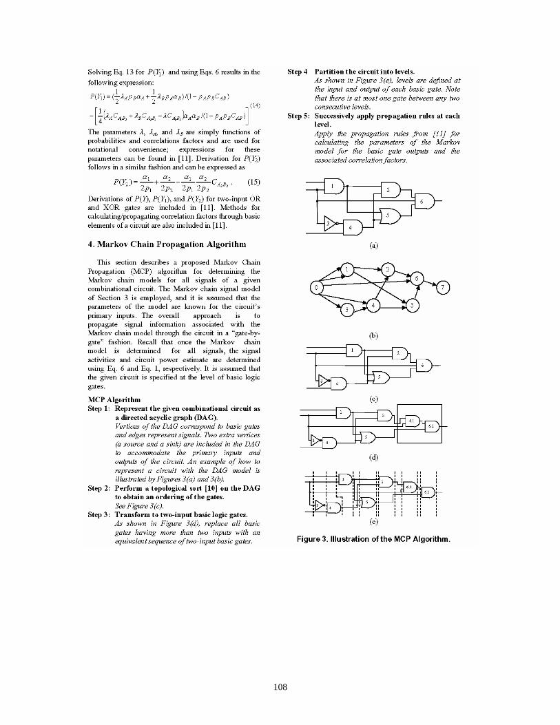
108
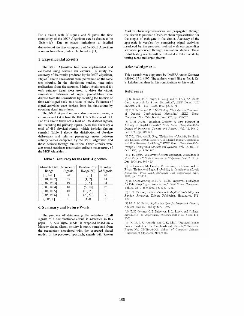
109
110
Appendix H: Nikhil D. Gupta, John K. Antonio, and Jack M. West, “Reconfigurable Computing for Space-Time Adaptive Processing” Proceedings of the Sixth Annual IEEE Symposium on Field Programmable Custom Computing Machines (FCCM), Napa, CA, USA, Apr. 1998, pp. 335-336.
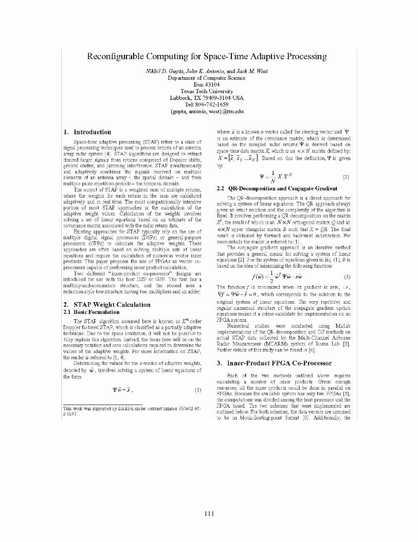
111
112
113
Appendix I: Jeffrey T. Muehring and John K. Antonio, “Minimizing Power Consumption using Signal Activity Transformations for Very Deep FPGA Pipelines,” Proceedings of the Military and Aerospace Applications for Programmable Devices and Technologies Conference (MAPLD 2000), sponsors: NASA and Johns Hopkins University/Applied Physics Laboratory, Laurel, MD, Sep. 2000.
114
115
116
117
Appendix J: S. Vanichayobon, Sudarshan K. Dhall, S. Lakshmivarahan, and John K. Antonio, “Power-speed Trade-off in Parallel Prefix Circuits,” Proceedings of ITComm 2002, High-Performance Pervasive Computing Conference, sponsor: SPIE, Boston, MA, July/Aug. 2002, pp. 109-120.
118
119
120
121
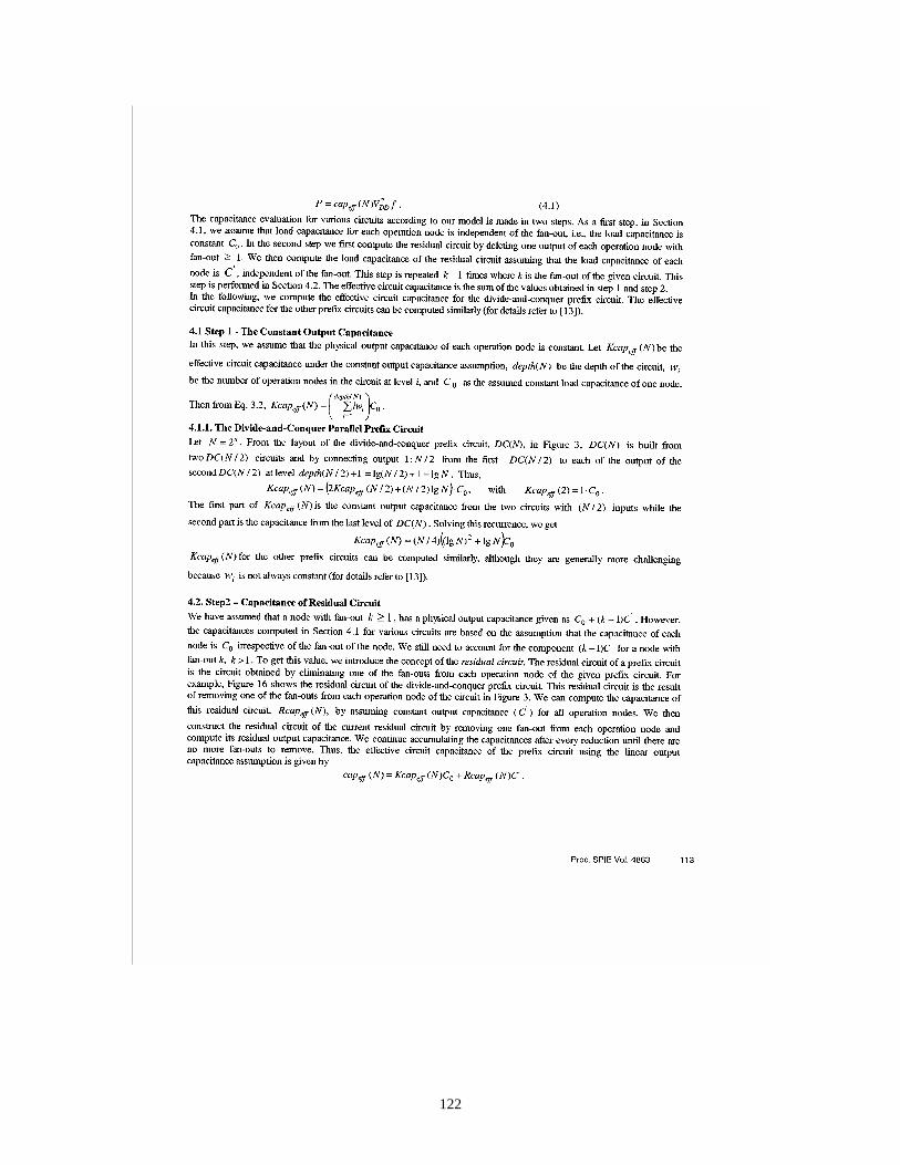
122
123
124
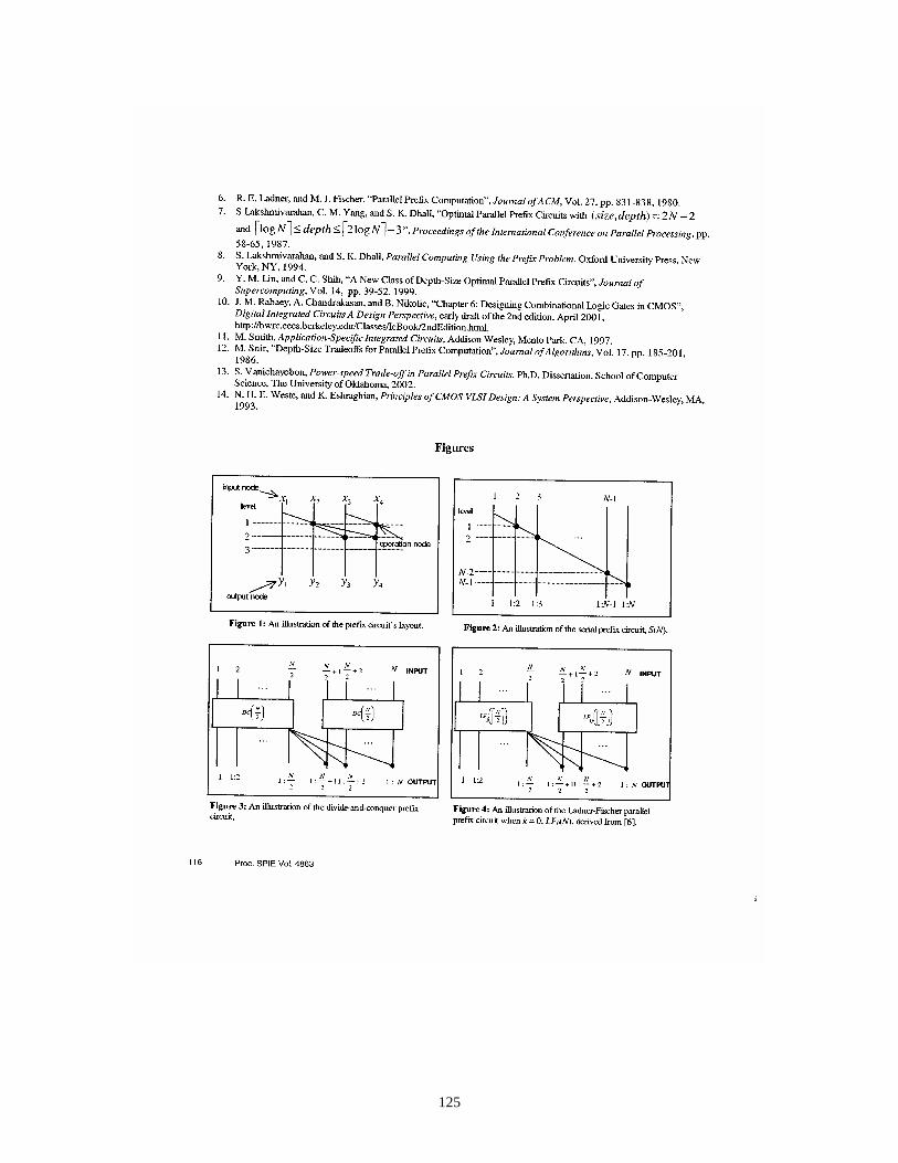
125
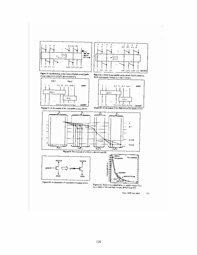
126
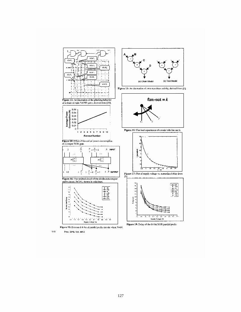
127
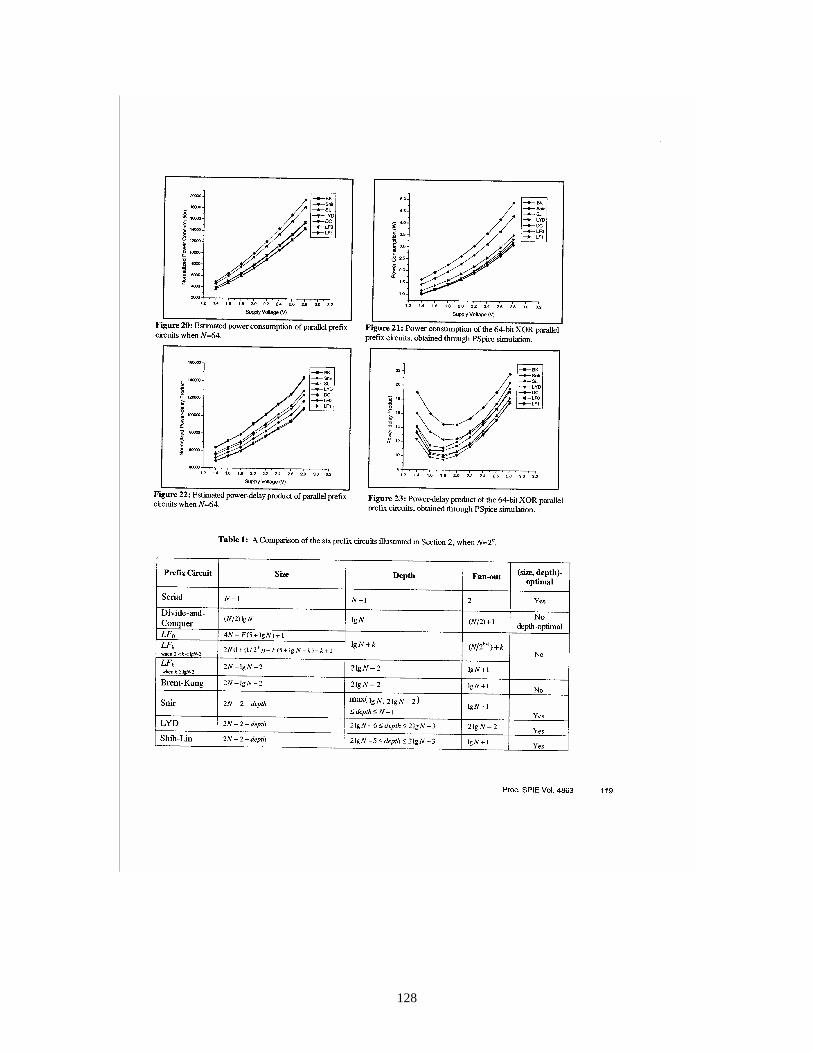
128
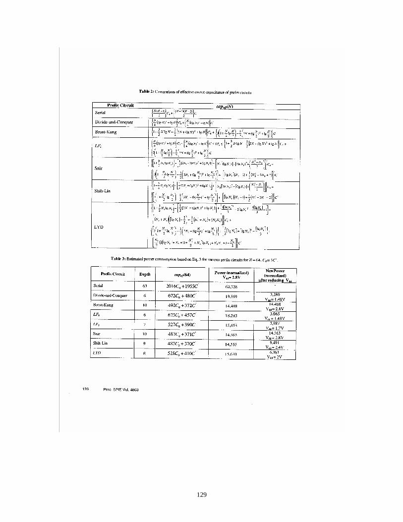
129
130
Appendix K: Jack M. West, Hongping Li, Sirirut Vanichayobon, Jeffrey T. Muehring, John K. Antonio, and Sudarshan K. Dhall, “A Hybrid FPGA/DSP/GPP Prototype Architecture for SAR and STAP,” Proceedings of the Fourth Annual High Performance Embedded Computing Workshop, sponsors: U.S. Navy and Defense Advanced Research Projects Agency (DARPA), MIT Lincoln Laboratory Publications, Group 18, Lexington, MA, Sep. 2000, pp. 29-30.
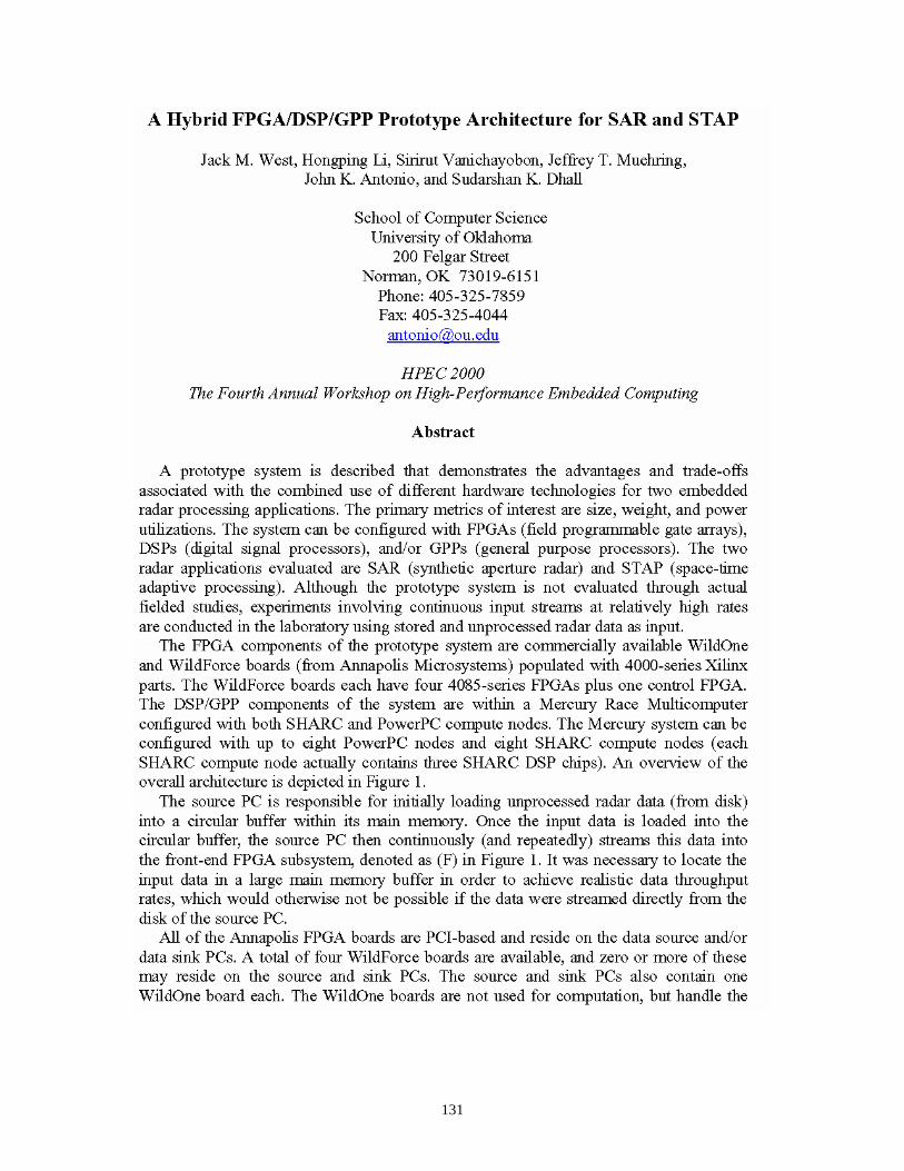
131
132
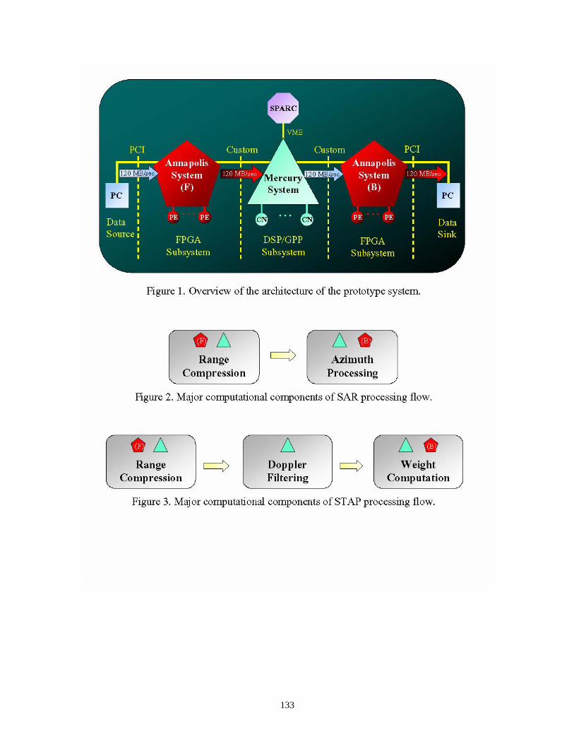
133