conga-sa5 user's guide · this user’s guide provides information about the components,...
TRANSCRIPT
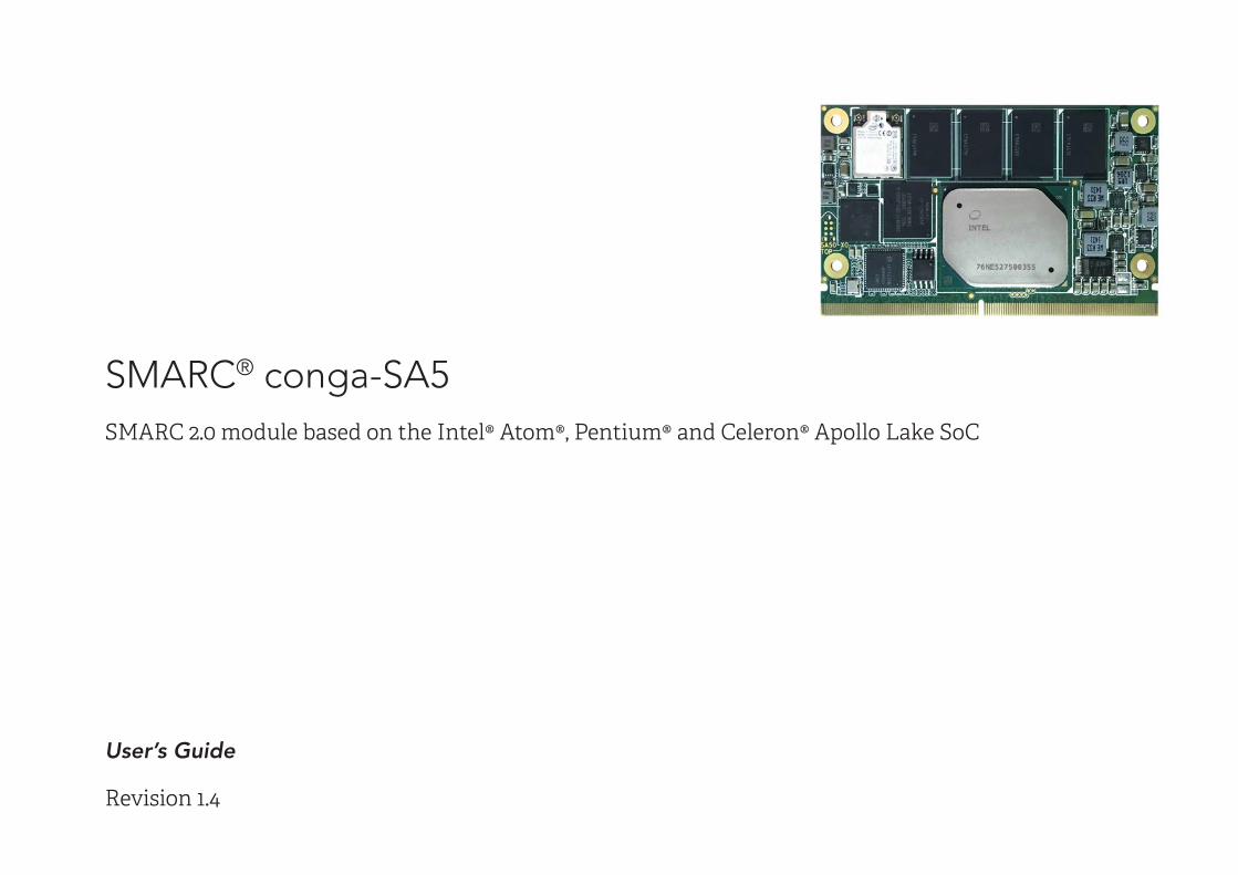
SMARC® conga-SA5SMARC 2.0 module based on the Intel® Atom®, Pentium® and Celeron® Apollo Lake SoC
User’s Guide
Revision 1.4
Copyright © 2017 congatec AG SA50m14.indd 2/72
Revision HistoryRevision Date (yyyy-mm-dd) Author Changes0.1 2017-08-16 AEM • Preliminary release
1.0 2017-10-20 AEM • Updated TPM support in tables 1 and 2 of section 1.2.1 “Options Information • Added TPM support to table 3 “Feature Summary” • Removed Android from supported OS in section 2.2 “Supported Operating Systems” • Updated table 5 “Power Consumptions Values” and table 6 “CMOS Battery Power Consumption” • Updated table 28 “GPIO Signal Description” • Added content to section 9 “System Resources” and section 10 “BIOS Setup Description” • Official release
1.1 2018.05.02 AEM • Updated “Electrostatic Sensitive Device” information on page 3 • Corrected the power consumption measurement unit in table 5 “Power Consumption Values” • Corrected the number of supported PCIe gen 2 lanes in section 1.2.1 “Options Information” • Corrected the onboard memory capacity of the variant with PN: 050010 in table 2 “conga-SA5 (Industrial Variants) • Added section 2.4.3 “Rise Time” • Corrected typographical error in table 30.1 “Boot Source Description” • Added EFT caution to section 5.5 “Universal Serial Bus (USB)” • Updated section 5.8 “UART” • Corrected the signal name of pin 37 in table 16 “SDIO Signal Descriptions” • Corrected the list of supported flash devices in section 10.4 “Supported Flash Devices“
1.2 2018.06.25 AEM • Added errata as a document to read in the preface section • Corrected the description of HDMI_HPD signal in table 14 “HDMI Signal Descriptions” • Updated tables 11 “SMARC Edge Finger Pinout“ and 18 “eSPI/SPI1 Signal Descriptions”
1.3 2018.08.21 AEM • Corrected the power consumption of Intel Pentium N4200 at peak value in table 5 “Power Consumption Values”
1.4 2018.10.29 AEM • Updated section 4 “Cooling Solutions” to reflect the new height of the fins • Added note about PCIe reference clocks in section 5.2 “PCIe Express™” • Added note about UART legacy mode in section 5.8 “UART” • Corrected the Winbond flash supported for external BIOS in section 10.4 “Supported Flash Devices”
Copyright © 2017 congatec AG SA50m14.indd 3/72
Preface
This user’s guide provides information about the components, features, connectors and BIOS Setup menus available on the conga-SA5. It is one of four documents that should be referred to when designing a SMARC® application. This user’s guide should be read in conjunction with the document “Errata_congatec_xA5_designs”. Click on the document name to download it.
The other reference documents that should be used include the following:
SMARC® Design Guide 2.0SMARC® Specification 2.0
The links to the SMARC® documents can be found on the SGET website at www.sget.org.
Disclaimer
The information contained within this user’s guide, including but not limited to any product specification, is subject to change without notice.
congatec AG provides no warranty with regard to this user’s guide or any other information contained herein and hereby expressly disclaims any implied warranties of merchantability or fitness for any particular purpose with regard to any of the foregoing. congatec AG assumes no liability for any damages incurred directly or indirectly from any technical or typographical errors or omissions contained herein or for discrepancies between the product and the user’s guide. In no event shall congatec AG be liable for any incidental, consequential, special, or exemplary damages, whether based on tort, contract or otherwise, arising out of or in connection with this user’s guide or any other information contained herein or the use thereof.
Intended Audience
This user’s guide is intended for technically qualified personnel. It is not intended for general audiences.
Lead-Free Designs (RoHS)
All congatec AG designs are created from lead-free components and are completely RoHS compliant.
Copyright © 2017 congatec AG SA50m14.indd 4/72
Electrostatic Sensitive Device
All congatec AG products are electrostatic sensitive devices. They are enclosed in static shielding bags, and shipped enclosed in secondary packaging (protective packaging). The secondary packaging does not provide electrostatic protection.
Do not remove the device from the static shielding bag or handle it, except at an electrostatic-free workstation. Also, do not ship or store electronic devices near strong electrostatic, electromagnetic, magnetic, or radioactive fields unless the device is contained within its original packaging. Be aware that failure to comply with these guidelines will void the congatec AG Limited Warranty.
Symbols
The following symbols are used in this user’s guide:
Warning
Warnings indicate conditions that, if not observed, can cause personal injury.
Caution
Cautions warn the user about how to prevent damage to hardware or loss of data.
Note
Notes call attention to important information that should be observed.
Copyright Notice
Copyright © 2017, congatec AG. All rights reserved. All text, pictures and graphics are protected by copyrights. No copying is permitted without written permission from congatec AG.
congatec AG has made every attempt to ensure that the information in this document is accurate yet the information contained within is supplied “as-is”.
Copyright © 2017 congatec AG SA50m14.indd 5/72
Trademarks
Product names, logos, brands, and other trademarks featured or referred to within this user’s guide, or the congatec website, are the property of their respective trademark holders. These trademark holders are not affiliated with congatec AG, our products, or our website.
Warranty
congatec AG makes no representation, warranty or guaranty, express or implied regarding the products except its standard form of limited warranty (“Limited Warranty”) per the terms and conditions of the congatec entity, which the product is delivered from. These terms and conditions can be downloaded from www.congatec.com. congatec AG may in its sole discretion modify its Limited Warranty at any time and from time to time.
The products may include software. Use of the software is subject to the terms and conditions set out in the respective owner’s license agreements, which are available at www.congatec.com and/or upon request.
Beginning on the date of shipment to its direct customer and continuing for the published warranty period, congatec AG represents that the products are new and warrants that each product failing to function properly under normal use, due to a defect in materials or workmanship or due to non conformance to the agreed upon specifications, will be repaired or exchanged, at congatec’s option and expense.
Customer will obtain a Return Material Authorization (“RMA”) number from congatec AG prior to returning the non conforming product freight prepaid. congatec AG will pay for transporting the repaired or exchanged product to the customer.
Repaired, replaced or exchanged product will be warranted for the repair warranty period in effect as of the date the repaired, exchanged or replaced product is shipped by congatec, or the remainder of the original warranty, whichever is longer. This Limited Warranty extends to congatec’s direct customer only and is not assignable or transferable.
Except as set forth in writing in the Limited Warranty, congatec makes no performance representations, warranties, or guarantees, either express or implied, oral or written, with respect to the products, including without limitation any implied warranty (a) of merchantability, (b) of fitness for a particular purpose, or (c) arising from course of performance, course of dealing, or usage of trade.
congatec AG shall in no event be liable to the end user for collateral or consequential damages of any kind. congatec shall not otherwise be liable for loss, damage or expense directly or indirectly arising from the use of the product or from any other cause. The sole and exclusive remedy against congatec, whether a claim sound in contract, warranty, tort or any other legal theory, shall be repair or replacement of the product only.
Copyright © 2017 congatec AG SA50m14.indd 6/72
Certification
congatec AG is certified to DIN EN ISO 9001 standard.
Technical Support
congatec AG technicians and engineers are committed to providing the best possible technical support for our customers so that our products can be easily used and implemented. We request that you first visit our website at www.congatec.com for the latest documentation, utilities and drivers, which have been made available to assist you. If you still require assistance after visiting our website then contact our technical support department by email at [email protected].
Terminology
Term DescriptionGB GigabyteGHz GigahertzkB KilobyteMB MegabyteMTps Mega-transfers per secondMbit Megabit kHz KilohertzMHz MegahertzTDP Thermal Design PowerPCIe PCI Express SATA Serial ATAPEG PCI Express GraphicsPCH Platform Controller HubeDP Embedded DisplayPortDDI Digital Display InterfaceHDA High Definition AudioN.C Not connectedN.A Not availableT.B.D To be determined
CERTIFICATION
ISO 9001
TM
Copyright © 2017 congatec AG SA50m14.indd 7/72
Contents1 Introduction ............................................................................. 10
1.1 SMARC® Concept .................................................................... 101.2 conga-SA5 Options Information .............................................. 101.2.1 Options Information ................................................................. 11
2 Specifications ........................................................................... 13
2.1 Feature List .............................................................................. 132.2 Supported Operating Systems ................................................ 142.3 Mechanical Dimensions ........................................................... 142.4 Standard Power ........................................................................ 152.4.1 Supply Voltage ......................................................................... 152.4.2 Electrical Characteristics .......................................................... 152.4.3 Rise Time ................................................................................. 152.5 Power Consumption ................................................................ 162.6 Supply Voltage Battery Power ................................................. 172.7 Environmental Specifications ................................................... 18
3 Block Diagram .......................................................................... 19
4 Cooling Solutions ..................................................................... 20
4.1 CSP Dimensions ....................................................................... 214.2 Heatspreader Dimensions ........................................................ 23
5 Connector Rows ....................................................................... 25
5.1 Display Interfaces ..................................................................... 255.1.1 LVDS ......................................................................................... 255.1.2 HDMI ........................................................................................ 265.1.3 DP ++ ...................................................................................... 265.2 PCI Express™ ........................................................................... 265.3 Gigabit Ethernet ...................................................................... 275.4 SATA ........................................................................................ 285.5 Universal Serial Bus (USB) ........................................................ 285.6 SD Card .................................................................................... 305.7 Audio (HDA / I2S) ..................................................................... 305.8 UART ........................................................................................ 30
5.9 GPIO ........................................................................................ 315.10 Communication Buses ............................................................. 315.10.1 SPI ............................................................................................ 315.10.2 I2C ........................................................................................... 315.10.3 I2S ............................................................................................ 315.11 Power Control .......................................................................... 32
6 Additional Features .................................................................. 34
6.1 Optional Onboard Interfaces ................................................... 346.2 Standard Onboard Interfaces .................................................. 346.2.1 congatec Board Controller (cBC) ............................................. 346.2.1.1 Board Information .................................................................... 346.2.1.2 General Purpose Input/Output ................................................ 356.2.1.3 Fan Control .............................................................................. 356.2.1.4 Power Loss Control .................................................................. 356.2.1.5 Watchdog ................................................................................ 356.2.1.6 I2C Bus ...................................................................................... 366.3 OEM BIOS Customization ........................................................ 366.3.1 OEM Default Settings .............................................................. 366.3.2 OEM Boot Logo ....................................................................... 366.3.3 OEM POST Logo ..................................................................... 366.3.4 OEM BIOS Code/Data ............................................................. 376.3.5 OEM DXE Driver ...................................................................... 376.4 congatec Battery Management Interface ................................ 376.5 API Support (CGOS) ................................................................ 386.6 Suspend to Ram ....................................................................... 38
7 conga Tech Notes .................................................................... 39
7.1 Intel® Apollo Lake SoC Features .............................................. 397.1.1 Processor Core ......................................................................... 397.1.1.1 Intel Virtualization Technology ................................................. 397.1.1.2 AHCI ........................................................................................ 407.1.1.3 Thermal Management ............................................................. 407.2 ACPI Suspend Modes and Resume Events .............................. 417.3 USB Port Mapping ................................................................... 42
Copyright © 2017 congatec AG SA50m14.indd 8/72
8 Signal Descriptions and Pinout Tables ..................................... 43
9 System Resources .................................................................... 66
9.1 I/O Address Assignment .......................................................... 669.2 PCI Configuration Space Map ................................................. 679.3 I²C Bus and SMBus .................................................................. 689.4 congatec System Sensors ........................................................ 69
10 BIOS Setup Description ........................................................... 70
10.1 Navigating the BIOS Setup Menu ........................................... 7010.2 BIOS Versions........................................................................... 7010.3 Updating the BIOS ................................................................... 7010.4 Supported Flash Devices ......................................................... 71
11 Industry Specifications ............................................................. 72
Copyright © 2017 congatec AG SA50m14.indd 9/72
List of TablesTable 1 conga-SA5 (Commercial Variants) ............................................ 11Table 2 conga-SA5 (Industrial Variants) ................................................ 12Table 3 Feature Summary ..................................................................... 13Table 4 Measurement Description ........................................................ 16Table 5 Power Consumption Values ..................................................... 17Table 6 CMOS Battery Power Consumption ........................................ 17Table 7 Display Combination .............................................................. 25Table 8 PCIe Reference Clock Configuration ....................................... 27Table 9 Possible USB Port Mapping ..................................................... 29Table 10 Wake Events ............................................................................. 41Table 11 Signal Tables Terminology Descriptions .................................. 43Table 12 SMARC Edge Finger Pinout ..................................................... 44Table 13 LVDS Signal Description .......................................................... 49Table 14 HDMI Signal Descriptions ........................................................ 52Table 15 DisplayPort++ .......................................................................... 53Table 16 MIPI CSI-2/-3 ............................................................................ 53Table 17 SDIO Signal Descriptions ......................................................... 54Table 18 SPI0 Signal Descriptions .......................................................... 55Table 19 eSPI/SPI1 Signal Descriptions .................................................. 55Table 20 I2S Signal Descriptions ............................................................ 56Table 21 HDA / I2S Signal Descriptions ................................................. 56Table 22 I2C Signal Descriptions ............................................................ 56Table 23 Asynchronous Serial Port Signal Description ........................... 57Table 24 USB Pinout Description ............................................................ 57Table 25 PCIe Signal Description ........................................................... 58Table 26 SATA Signal Description .......................................................... 59Table 27 Gigabit Ethernet Signal Description ........................................ 60Table 28 Watchdog Signal Description .................................................. 61Table 29 GPIO Signal Description .......................................................... 61Table 30 Management Pins Signal Description ...................................... 62Table 31 Boot Select Signal Description ................................................ 63Table 32 Power and GND Signal Descriptions ....................................... 65Table 33 I/O Address Assignment .......................................................... 66Table 34 PCI Configuration Space Map ................................................. 67Table 35 Bus Accessibility ....................................................................... 68Table 36 References ............................................................................... 72
Copyright © 2017 congatec AG SA50m14.indd 10/72
1 Introduction
1.1 SMARC® Concept
The Standardization Group for Embedded Technologies e.V (SGET) defined the SMARC standard for small form factor computer modules that target applications with ultra low power, low cost and high performance. The SMARC connector and interfaces are optimized for high-speed communication, and are suitable for ARM SoCs and low power x86 SoCs.
The SMARC standard bridges the gap between the COM Express standard and the Qseven standard by offering most of the interfaces defined in the COM Express specification at a lower power. With a footprint of 82 mm x 50 mm or 82 mm x 80 mm, the SMARC standard promotes the design of highly integrated, energy efficient systems.
Due to its small size and lower power demands, PC appliance designers can design low cost devices as well as explore a huge variety of product development options—from compact space-saving designs to fully functional systems. This solution allows scalability, product diversification and faster time to market.
1.2 conga-SA5 Options Information
The conga-SA5 is designed based on the SMARC 2.0 Specification. The conga-SA5 features the Intel Atom, Pentium and Celeron Apollo Lake SoCs. With maximum 12 W TDP, the conga-SA5 offers Ultra Low Power boards with high computing performance and outstanding graphics. Additionally, the conga-SA5 supports quad channel LPDDR4 memory with up 8 GB capacity and data rates up to 2400 MTps, multiple I/O interfaces, up to three independent displays and various congatec embedded features.
By offering most of the functional requirement for any SMARC application, the conga-SA5 provides manufacturers and developers with a platform to jump-start the development of systems and applications based on SMARC specification. Its features and capabilities make it an ideal platform for designing compact, energy-efficient, performance-oriented embedded systems.
Copyright © 2017 congatec AG SA50m14.indd 11/72
1.2.1 Options Information
The conga-SA5 is available in eight variants (five commercial and three industrial). The table below shows the different configurations available.
Table 1 conga-SA5 (Commercial Variants)
Part-No 050000 050001 050002 050022 050023Processor Intel® Atom® x7-E3950,
1.6 GHz, Quad CoreIntel® Atom® x5-E3940,1.6 GHz, Quad Core
Intel® Atom® x5-E3930,1.3 GHz, Dual Core
Intel® Celeron® N3350,1.1 GHz, Dual Core
Intel® Pentium® N4200,1.1 GHz, Quad Core
Burst Freq. 2.0 GHz 1.8 GHz 1.8 GHz 2.4 GHz 2.5 GHzL2 Cache 2 MB 2 MB 2 MB 2 MB 2 MB Graphics Engine Intel® HD Graphics 505 Intel® HD Graphics 500 Intel® HD Graphics 500 Intel® HD Graphics 500 Intel® HD Graphics 505GFX Base/Burst Freq. 500 / 650 MHz 400 / 600 MHz 400 / 550 MHz 200 / 650 200 / 750Onboard Memory(LPDDR4)
8 GB, 2400 MTpsquad channel
4 GB, 2133 MTpsquad channel
2 GB, 2133 MTpsdual channel
4 GB, 2400 MTpsquad channel
8 GB, 2400 MTpsquad channel
PCIe 4x Gen2 4x Gen2 4x Gen2 4x Gen2 4x Gen2Ethernet 2x i211 2x i211 2x i211 2x i211 2x i211Display Interfaces
LVDS Single/Dual 18/24bit Single/Dual 18/24bit Single/Dual 18/24bit Single/Dual 18/24bit Single/Dual 18/24bitDP++ 1x DP++ 1x DP++ 1x DP++ 1x DP++ 1x DP++HDMI 1x native HDMI 1x native HDMI 1x native HDMI 1x native HDMI 1x native HDMI
USB ports 4x USB 2.02x USB 3.0/2.0
4x USB 2.02x USB 3.0/2.0
4x USB 2.02x USB 3.0/2.0
4x USB 2.02x USB 3.0/2.0
4x USB 2.02x USB 3.0/2.0
eMMC 32 GB, MLC 32 GB, MLC 16 GB, MLC 32 GB, MLC 32 GB, MLCWifi/BT Module N.A N.A N.A N.A N.ATPM Firmware Intel PTT Intel PTT Intel PTT Intel PTT Intel PTT
Discrete N.A N.A N.A N.A N.ASD Card 1x 4-bit 1x 4-bit 1x 4-bit 1x 4-bit 1x 4-bitMax. TDP 12 W 9.5 W 6.5 W 6 W 6 W
Copyright © 2017 congatec AG SA50m14.indd 12/72
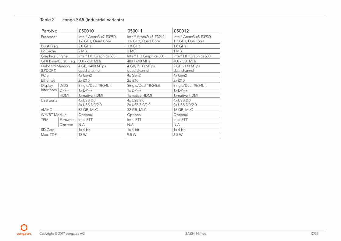
Table 2 conga-SA5 (Industrial Variants)
Part-No 050010 050011 050012Processor Intel® Atom® x7-E3950,
1.6 GHz, Quad CoreIntel® Atom® x5-E3940,1.6 GHz, Quad Core
Intel® Atom® x5-E3930,1.3 GHz, Dual Core
Burst Freq. 2.0 GHz 1.8 GHz 1.8 GHzL2 Cache 2 MB 2 MB 1 MB Graphics Engine Intel® HD Graphics 505 Intel® HD Graphics 500 Intel® HD Graphics 500GFX Base/Burst Freq. 500 / 650 MHz 400 / 600 MHz 400 / 550 MHzOnboard Memory(LPDDR4)
4 GB, 2400 MTpsquad channel
4 GB, 2133 MTpsquad channel
2 GB 2133 MTpsdual channel
PCIe 4x Gen2 4x Gen2 4x Gen2Ethernet 2x i210 2x i210 2x i210Display Interfaces
LVDS Single/Dual 18/24bit Single/Dual 18/24bit Single/Dual 18/24bitDP++ 1x DP++ 1x DP++ 1x DP++HDMI 1x native HDMI 1x native HDMI 1x native HDMI
USB ports 4x USB 2.02x USB 3.0/2.0
4x USB 2.02x USB 3.0/2.0
4x USB 2.02x USB 3.0/2.0
eMMC 32 GB, MLC 32 GB, MLC 16 GB, MLCWifi/BT Module Optional Optional OptionalTPM Firmware Intel PTT Intel PTT Intel PTT
Discrete N.A N.A N.ASD Card 1x 4-bit 1x 4-bit 1x 4-bitMax. TDP 12 W 9.5 W 6.5 W
Copyright © 2017 congatec AG SA50m14.indd 13/72
2 Specifications
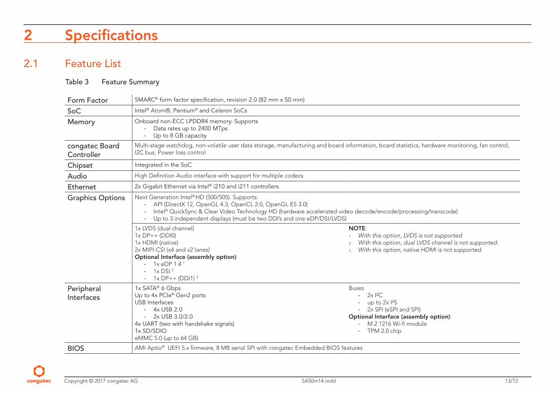
2.1 Feature List
Table 3 Feature Summary
Form Factor SMARC® form factor specification, revision 2.0 (82 mm x 50 mm)
SoC Intel® Atom®, Pentium® and Celeron SoCs
Memory Onboard non-ECC LPDDR4 memory. Supports - Data rates up to 2400 MTps - Up to 8 GB capacity
congatec Board Controller
Multi-stage watchdog, non-volatile user data storage, manufacturing and board information, board statistics, hardware monitoring, fan control, I2C bus, Power loss control
Chipset Integrated in the SoC
Audio High Definition Audio interface with support for multiple codecs
Ethernet 2x Gigabit Ethernet via Intel® i210 and i211 controllers
Graphics Options Next Generation Intel® HD (500/505). Supports: - API (DirectX 12, OpenGL 4.3, OpenCL 2.0, OpenGL ES 3.0) - Intel® QuickSync & Clear Video Technology HD (hardware accelerated video decode/encode/processing/transcode) - Up to 3 independent displays (must be two DDI’s and one eDP/DSI/LVDS)
1x LVDS (dual channel)1x DP++ (DDI0)1x HDMI (native)2x MIPI-CSI (x4 and x2 lanes)Optional Interface (assembly option):
- 1x eDP 1.4 1
- 1x DSI 2
- 1x DP++ (DDI1) 3
NOTE:1 With this option, LVDS is not supported2 With this option, dual LVDS channel is not supported. 3 With this option, native HDMI is not supported.
Peripheral Interfaces
1x SATA® 6 GbpsUp to 4x PCIe® Gen2 portsUSB Interfaces
- 4x USB 2.0 - 2x USB 3.0/2.0
4x UART (two with handshake signals)1x SD/SDIOeMMC 5.0 (up to 64 GB)
Buses - 2x I²C - up to 2x I²S - 2x SPI (eSPI and SPI)
Optional Interface (assembly option): - M.2 1216 Wi-fi module - TPM 2.0 chip
BIOS AMI Aptio® UEFI 5.x firmware, 8 MB serial SPI with congatec Embedded BIOS features
Copyright © 2017 congatec AG SA50m14.indd 14/72
Power Mgmt. ACPI 5.0 compliant with battery support. Also supports Suspend to RAM (S3)
Security Firmware TPM 2.0 (Intel® PTT)Discrete LPC TPM 2.0 (Infineon SLB9665) or LPC TPM 1.2 (Infineon SLB9660) support via assembly option
Note
Some of the features mentioned in the above Feature Summary are optional. Check the article number of your module and compare it to the option information list on page 11 to determine what options are available on your particular module.
2.2 Supported Operating Systems
The conga-SA5 supports the following operating systems.
• Microsoft® Windows® 10 IoT Enterprise
• Microsoft® Windows® IoT Core
• Microsoft® Windows® 10
• Linux 3.x / 4.x
• Yocto 2.x
Note
To install Windows® 10, you require a minimum storage capacity of 20 GB. We will not offer installation support for systems with less than 20 GB storage space.
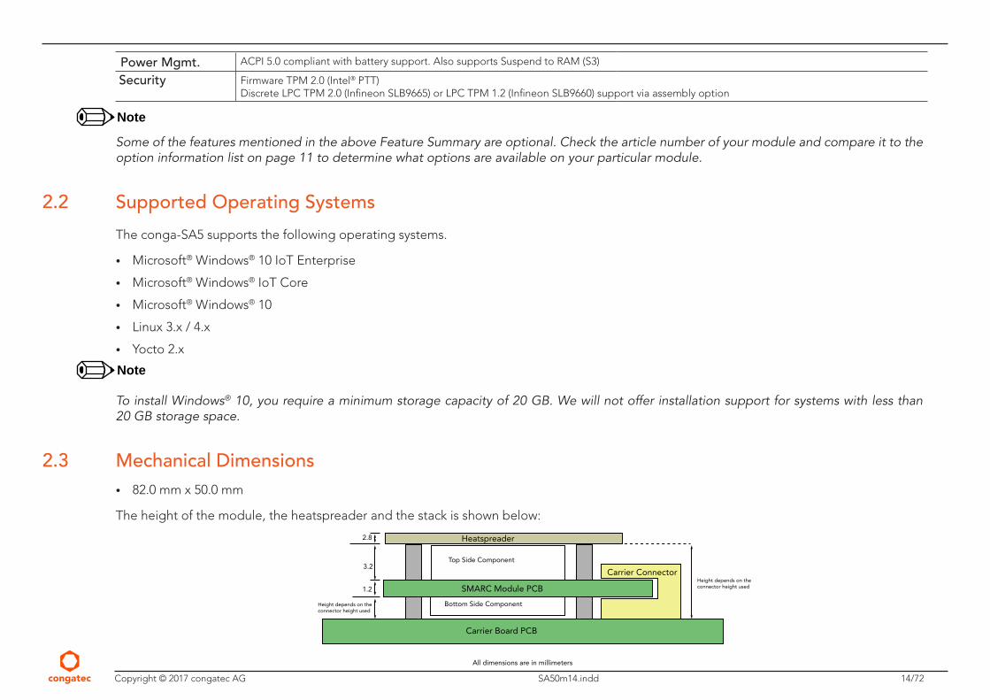
2.3 Mechanical Dimensions • 82.0 mm x 50.0 mm
The height of the module, the heatspreader and the stack is shown below:
Top Side Component
Carrier Board PCB
SMARC Module PCB
Heatspreader
Carrier Connector
Bottom Side Component
All dimensions are in millimeters
Height depends on theconnector height used
Height depends on theconnector height used 1.2
3.2
2.8
Copyright © 2017 congatec AG SA50m14.indd 15/72
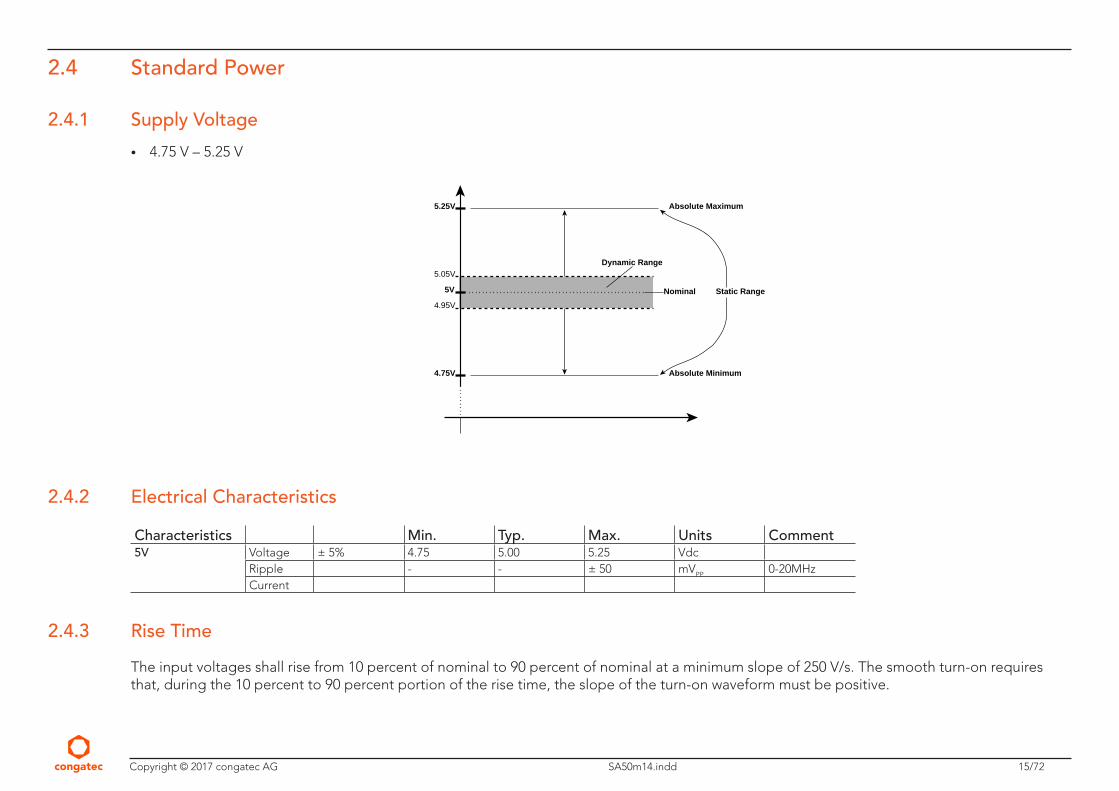
2.4 Standard Power
2.4.1 Supply Voltage
• 4.75 V – 5.25 V
2.4.2 Electrical Characteristics
Characteristics Min. Typ. Max. Units Comment5V Voltage ± 5% 4.75 5.00 5.25 Vdc
Ripple - - ± 50 mVPP 0-20MHzCurrent
2.4.3 Rise Time
The input voltages shall rise from 10 percent of nominal to 90 percent of nominal at a minimum slope of 250 V/s. The smooth turn-on requires that, during the 10 percent to 90 percent portion of the rise time, the slope of the turn-on waveform must be positive.
Nominal Static Range
Dynamic Range
Absolute Minimum
Absolute Maximum5.25V
4.75V
5V
5.05V
4.95V
Copyright © 2017 congatec AG SA50m14.indd 16/72
2.5 Power Consumption
The power consumption values were measured with the following setup:
• conga-SA5 COM
• conga-SEVA (supplied with two different power supplies at the same time)
• conga-SA5 cooling solution
• Microsoft Windows 10 (64 bit)
Table 4 Measurement Description
The power consumption values were recorded during the following system states:
System State Description CommentS0: Minimum value Lowest frequency mode (LFM) with minimum core voltage during
desktop idle. S0: Maximum value Highest frequency mode (HFM/Turbo Boost). The CPU was stressed to its maximum frequency.S0: Peak value Highest power spike during the measurement of “S0: Maximum value”.
This state shows the peak value over a short period of time (worst case power consumption value).
Consider this value when designing the system’s power supply to ensure that sufficient power is supplied during worst case scenarios.
S3 COM is powered by VCC_5V, while in Suspend to RAM state.S5 COM is powered by VCC_5V, while in Soft-Off state
Note
The peripherals did not influence the measured values because they were powered externally.
Copyright © 2017 congatec AG SA50m14.indd 17/72
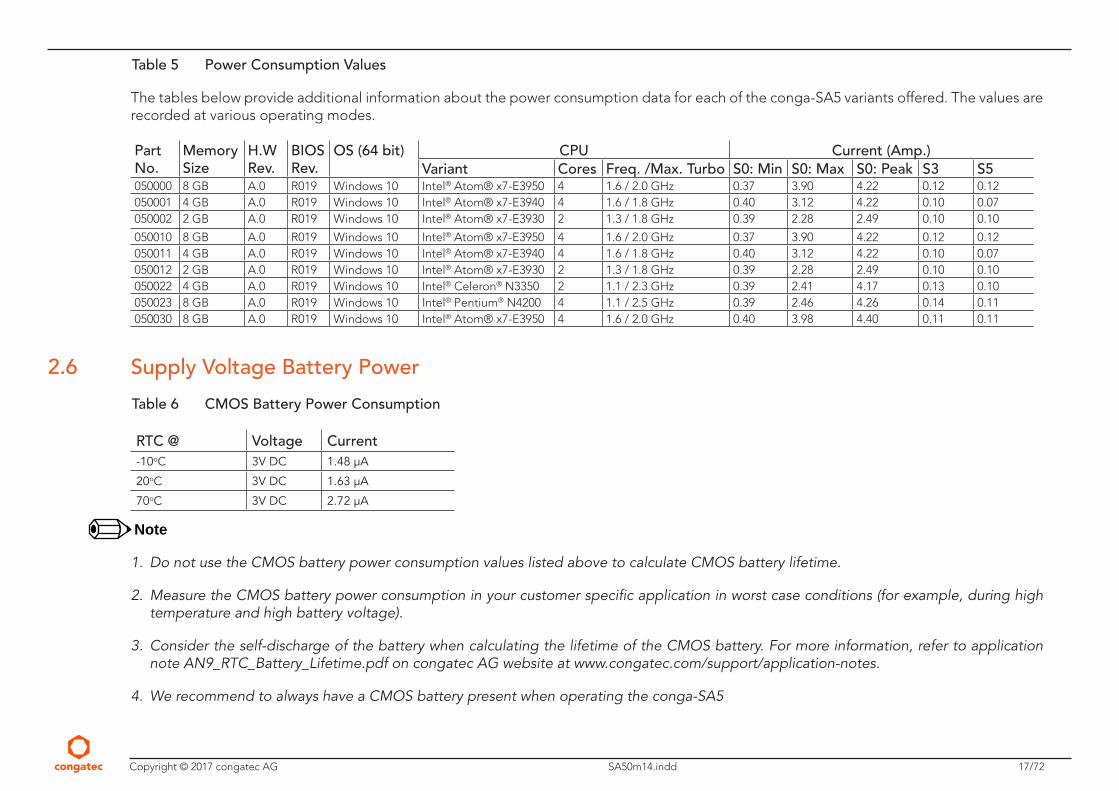
Table 5 Power Consumption Values
The tables below provide additional information about the power consumption data for each of the conga-SA5 variants offered. The values are recorded at various operating modes.
Part No.
Memory Size
H.W Rev.
BIOS Rev.
OS (64 bit) CPU Current (Amp.)Variant Cores Freq. /Max. Turbo S0: Min S0: Max S0: Peak S3 S5
050000 8 GB A.0 R019 Windows 10 Intel® Atom® x7-E3950 4 1.6 / 2.0 GHz 0.37 3.90 4.22 0.12 0.12050001 4 GB A.0 R019 Windows 10 Intel® Atom® x7-E3940 4 1.6 / 1.8 GHz 0.40 3.12 4.22 0.10 0.07050002 2 GB A.0 R019 Windows 10 Intel® Atom® x7-E3930 2 1.3 / 1.8 GHz 0.39 2.28 2.49 0.10 0.10
050010 8 GB A.0 R019 Windows 10 Intel® Atom® x7-E3950 4 1.6 / 2.0 GHz 0.37 3.90 4.22 0.12 0.12050011 4 GB A.0 R019 Windows 10 Intel® Atom® x7-E3940 4 1.6 / 1.8 GHz 0.40 3.12 4.22 0.10 0.07050012 2 GB A.0 R019 Windows 10 Intel® Atom® x7-E3930 2 1.3 / 1.8 GHz 0.39 2.28 2.49 0.10 0.10050022 4 GB A.0 R019 Windows 10 Intel® Celeron® N3350 2 1.1 / 2.3 GHz 0.39 2.41 4.17 0.13 0.10050023 8 GB A.0 R019 Windows 10 Intel® Pentium® N4200 4 1.1 / 2.5 GHz 0.39 2.46 4.26 0.14 0.11050030 8 GB A.0 R019 Windows 10 Intel® Atom® x7-E3950 4 1.6 / 2.0 GHz 0.40 3.98 4.40 0.11 0.11
2.6 Supply Voltage Battery Power
Table 6 CMOS Battery Power Consumption
RTC @ Voltage Current-10oC 3V DC 1.48 µA
20oC 3V DC 1.63 µA
70oC 3V DC 2.72 µA
Note
1. Do not use the CMOS battery power consumption values listed above to calculate CMOS battery lifetime.
2. Measure the CMOS battery power consumption in your customer specific application in worst case conditions (for example, during high temperature and high battery voltage).
3. Consider the self-discharge of the battery when calculating the lifetime of the CMOS battery. For more information, refer to application note AN9_RTC_Battery_Lifetime.pdf on congatec AG website at www.congatec.com/support/application-notes.
4. We recommend to always have a CMOS battery present when operating the conga-SA5
Copyright © 2017 congatec AG SA50m14.indd 18/72
2.7 Environmental Specifications
Temperature (commercial variants) Operation: 0° to 60°C Storage: -20° to +80°C
Temperature (industrial variants) Operation: -40° to 85°C Storage: -45° to +85°C
Humidity Operation: 10% to 90% Storage: 5% to 95%
Caution
The above operating temperatures must be strictly adhered to at all times. When using a congatec heatspreader, the maximum operating temperature refers to any measurable spot on the heatspreader’s surface.
Humidity specifications are for non-condensing conditions.
Copyright © 2017 congatec AG SA50m14.indd 19/72
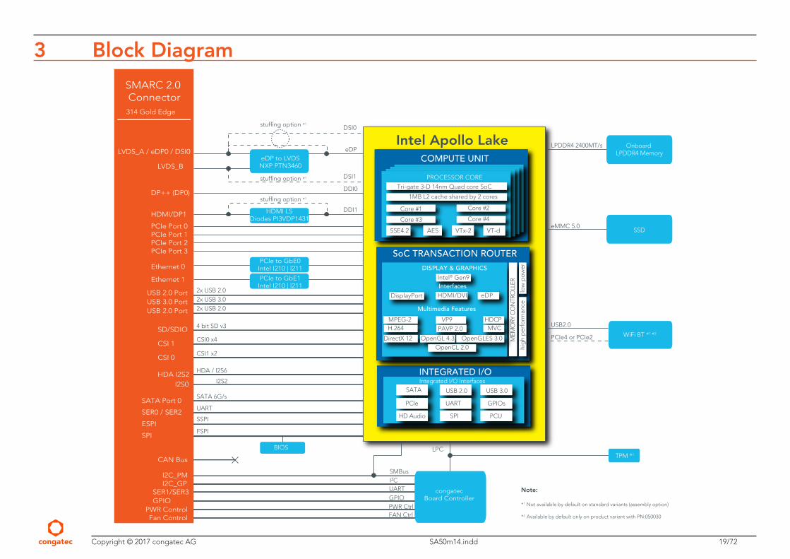
3 Block Diagram
Intel Apollo Lake
PAVP 2.0
OpenCL 2.0
Interfaces
SATA
SoC TRANSACTION ROUTER
USB 2.0
COMPUTE UNIT
Core #1 Core #2
Core #4
Tri-gate 3-D 14nm Quad core SoC
1MB L2 cache shared by 2 cores
PROCESSOR CORE
Core #3
AES VTx-2 VT-dSSE4.2
Multimedia Features
Intel® Gen9
DisplayPort HDMI/DVI eDP
MPEG-2H.264
DirectX 12
VP9 HDCPMVC
low
po
wer
hig
h p
erfo
rman
ce
DISPLAY & GRAPHICS
MEM
ORY
CO
NTR
OLL
ER
OpenGL 4.3 OpenGLES 3.0
UARTPCIe GPIOs
SPIHD Audio PCU
USB 3.0
Integrated I/O InterfacesINTEGRATED I/O
SATA 6G/s
UART
SSPI
FSPI
SMBusI²CUARTGPIOPWR CtrlFAN Ctrl
4 bit SD v3
CSI0 x4
CSI1 x2
HDA / I2S6
*1 Not available by default on standard variants (assembly option)
*2 Available by default only on product variant with PN:050030
Note:
I2S2
2x USB 2.02x USB 3.02x USB 2.0
LPDDR4 2400MT/s
eMMC 5.0
LPC
Onboard LPDDR4 Memory
USB2.0
PCIe4 or PCIe2 WiFi BT *1 *2
SSD
eDP to LVDSNXP PTN3460
HDMI LSDiodes PI3VDP1431
stuffing option *1
stuffing option *1
stuffing option *1
eDP
DSI0
DSI1
DDI0
DDI1
PCIe to GbE0Intel I210 | l211
PCIe to GbE1Intel I210 | l211
BIOS
congatecBoard Controller
TPM *1
Ethernet 0
Ethernet 1
LVDS_A / eDP0 / DSI0
LVDS_B
SMARC 2.0 Connector
314 Gold Edge
CAN Bus
SER0 / SER2
ESPI
SPI
HDA I2S2 I2S0
USB 2.0 PortUSB 3.0 PortUSB 2.0 Port
SATA Port 0
SD/SDIO
CSI 1
CSI 0
PWR Control
SER1/SER3GPIO
I2C_GPI2C_PM
Fan Control
PCIe Port 2PCIe Port 3
PCIe Port 1PCIe Port 0
DP++ (DP0)
HDMI/DP1
Copyright © 2017 congatec AG SA50m14.indd 20/72
4 Cooling Solutionscongatec AG offers the following cooling solutions for the conga-SA5 commercial and industrial variants:
• Passive cooling solution (CSP)
• Heatspreader
The dimensions of the cooling solutions are shown below. All measurements are in millimeters. The mechanical system assembly mounting shall follow the valid DIN/ISO specifications. The recommended maximum torque specification for all screws is 0.3 Nm.
Note
The gap pad material used on all congatec heatspreaders contains silicon oil that can seep out over time depending on the environmental conditions it is subjected to. For more information about this subject, contact your local congatec sales representative and request the gap pad material manufacturer’s specification.
Caution
The congatec heatspreaders/cooling solutions are tested only within the commercial temperature range of 0° to 60°C. Therefore, if your application that features a congatec heatspreader/cooling solution operates outside this temperature range, ensure the correct operating temperature of the module is maintained at all times. This may require additional cooling components for your final application’s thermal solution.
For adequate heat dissipation, use the mounting holes on the cooling solution to attach it to the module. Apply thread-locking fluid on the screws if the cooling solution is used in a high shock and/or vibration environment. To prevent the standoff from stripping or cross-threading, use threaded carrier board standoffs to mount non-threaded cooling solutions.
For applications that require vertically-mounted cooling solution, use only coolers that secure the thermal stacks with fixing post. Without the fixing post feature, the thermal stacks may move.
Also, do not exceed the maximum torque specified for the screws. Doing so may damage the module or the carrier board or both.
Copyright © 2017 congatec AG SA50m14.indd 21/72
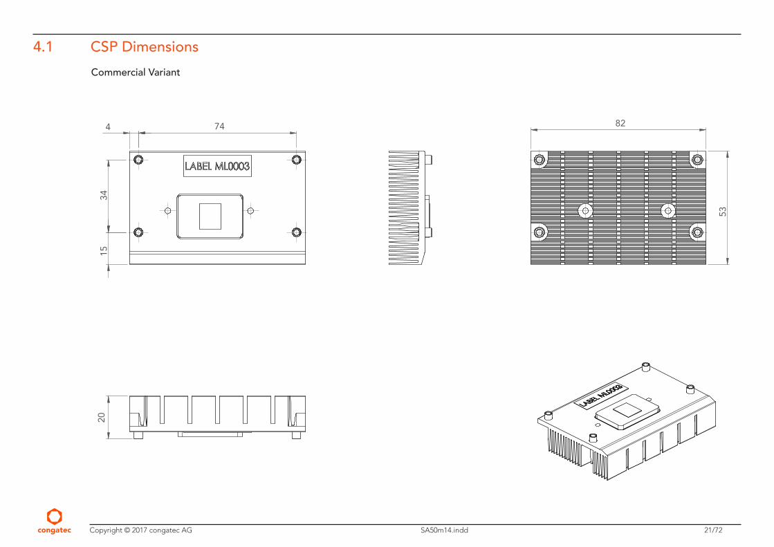
4.1 CSP Dimensions
Commercial Variant
15
34
74 4
53
82
20
Copyright © 2017 congatec AG SA50m14.indd 22/72
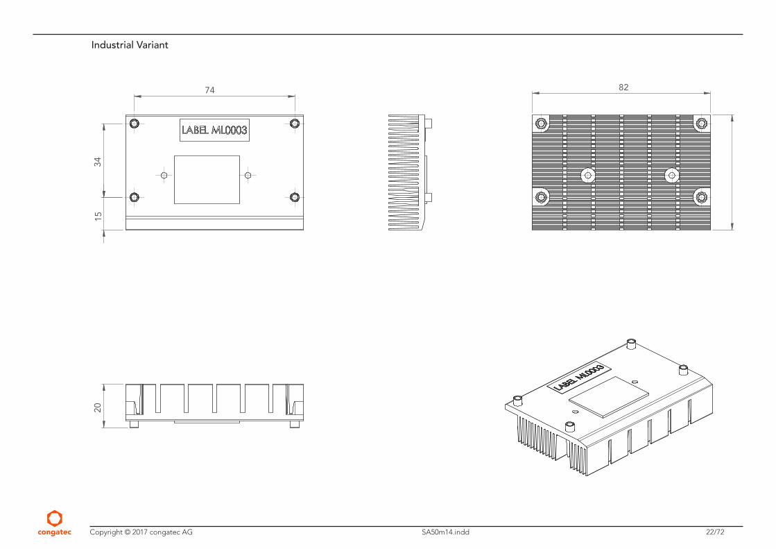
Industrial Variant
15
74 82 3
4 20
Copyright © 2017 congatec AG SA50m14.indd 23/72
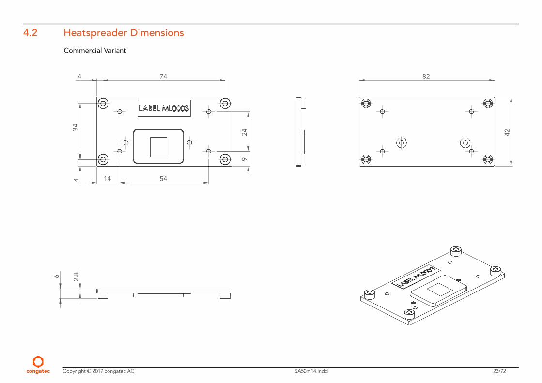
4.2 Heatspreader Dimensions
Commercial Variant
74 4
3
4
14 54
24
9
4
42
82
6
2.8
Copyright © 2017 congatec AG SA50m14.indd 24/72
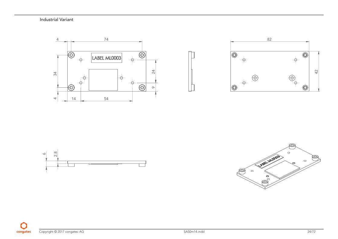
Industrial Variant
74
4
14 54
24
34
9
4
42
82 6
2.8
Copyright © 2017 congatec AG SA50m14.indd 25/72
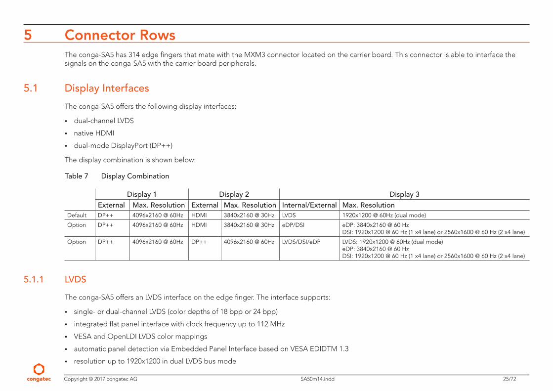
5 Connector RowsThe conga-SA5 has 314 edge fingers that mate with the MXM3 connector located on the carrier board. This connector is able to interface the signals on the conga-SA5 with the carrier board peripherals.
5.1 Display Interfaces
The conga-SA5 offers the following display interfaces:
• dual-channel LVDS
• native HDMI
• dual-mode DisplayPort (DP++)
The display combination is shown below:
Table 7 Display Combination
Display 1 Display 2 Display 3External Max. Resolution External Max. Resolution Internal/External Max. Resolution
Default DP++ 4096x2160 @ 60Hz HDMI 3840x2160 @ 30Hz LVDS 1920x1200 @ 60Hz (dual mode)
Option DP++ 4096x2160 @ 60Hz HDMI 3840x2160 @ 30Hz eDP/DSI eDP: 3840x2160 @ 60 HzDSI: 1920x1200 @ 60 Hz (1 x4 lane) or 2560x1600 @ 60 Hz (2 x4 lane)
Option DP++ 4096x2160 @ 60Hz DP++ 4096x2160 @ 60Hz LVDS/DSI/eDP LVDS: 1920x1200 @ 60Hz (dual mode)eDP: 3840x2160 @ 60 HzDSI: 1920x1200 @ 60 Hz (1 x4 lane) or 2560x1600 @ 60 Hz (2 x4 lane)
5.1.1 LVDS
The conga-SA5 offers an LVDS interface on the edge finger. The interface supports:
• single- or dual-channel LVDS (color depths of 18 bpp or 24 bpp)
• integrated flat panel interface with clock frequency up to 112 MHz
• VESA and OpenLDI LVDS color mappings
• automatic panel detection via Embedded Panel Interface based on VESA EDIDTM 1.3
• resolution up to 1920x1200 in dual LVDS bus mode
Copyright © 2017 congatec AG SA50m14.indd 26/72
Note
1. LVDS channel A (first channel) supports an optional eDP or MIPI DSI interface (assembly option).
2. Variants with optional eDP or MIPI DSI interface do not support LVDS interface
3. Only one MIPI DSI panel is supported (maximum of two channels, with up to four lanes each)
5.1.2 HDMI
The conga-SA5 offers a native HDMI interface. The interface supports:
• HDMI 1.4b specification
• resolutions up to 3840x2160 @ 30 Hz
Note
1. The HDMI interface supports an optional dual-mode DisplayPort interface (assembly option).
2. Variants with optional dual-mode DisplayPort do not support native HDMI voltage levels.
5.1.3 DP ++
The conga-SA5 offers a dual-mode DisplayPort (DP++). The interface supports:
• DisplayPort 1.2 specification
• resolutions up to 4096x2160 @ 60 Hz
5.2 PCI Express™
The conga-SA5 offers up to four PCI Express™ lanes. The lanes support:
• up to 5 GT/s (Gen 2) speed
• a 4 x1 link configuration (default)
• optional 1 x4 or 2 x2 or 1 x2 + 2 x1 1 link configuration (require customized BIOS firmware)
• lane polarity inversion
Copyright © 2017 congatec AG SA50m14.indd 27/72
Note
1. Possible with an assembly option.
The conga-SA5 provides up to three PCIe reference clocks to the carrier board. The table below shows the possible PCIe reference clock configurations.
Table 8 PCIe Reference Clock Configuration
PCIe Device Configuration Reference Clock Provided to Carrier BoardNo Wifi, no GbE PCIe_A_REFCK
PCIe_B_REFCK PCIe_C_REFCK
Wifi only PCIe_A_REFCKPCIe_B_REFCK PCIe_C_REFCK
GbE0 PCIe_A_REFCK PCIe_B_REFCK PCIe_C_REFCK
GbE0 + Wifi PCIe_A_REFCK PCIe_B_REFCK
GBE0 + GBE1 PCIe_A_REFCK PCIe_B_REFCK
GBE0 + GBE1 + WiFi PCIe_A_REFCK
Note
The number of reference clocks it provides depends on the number of on-module PCIe devices (Gbe, Wifi). For example, variants with one PCIe device will offer three PCIe reference clocks while variants with two on-module PCIe devices will offer two reference clocks for carrier board usage.
5.3 Gigabit Ethernet
The conga-SA5 offers two Gigabit Ethernet interfaces— via Intel® i210 and i211 controllers. The interfaces support full-duplex operation at 10/100/1000 Mbps and half-duplex operation at 10/100 Mbps.
Copyright © 2017 congatec AG SA50m14.indd 28/72
5.4 SATA
The conga-SA5 offers one SATA interface on the edge finger. The interface supports:
• SATA specification 3.2
• independent DMA operation
• data transfer rates up to 6.0 Gb/s
• AHCI mode using memory space
Note
The interface does not support legacy mode using I/O space.
5.5 Universal Serial Bus (USB)
The conga-SA5 offers the following USB interfaces:
• four USB 2.0 with support for:
– USB 1.1 and 2.0 specifications
– up to 480 Mbps data transfer
– high-speed, full-speed and low-speed signalling
– additional two ports if SuperSpeed ports are not implemented
• two USB 3.0/2.0 with support for:
– USB 3.0 specification
– up to 5 Gbps data transfer
– SuperSpeed, high-speed, full-speed and low-speed signalling
– optional dual-role support on USB port 3 (assembly option)
Copyright © 2017 congatec AG SA50m14.indd 29/72
Table 9 Possible USB Port Mapping
USB 2.0 USB 3.0/2.0Host Only Dual Role Host Only Dual Role
Default 3 ports 1 port 2 port -
Option 4 ports - 1 port 1 port
Option 4 ports - 2 ports -
Option 6 ports - - -
Note
For USB 3.0 support on your carrier board, pair USB 2.0 port 2 or 3 or both with the SuperSpeed signals.
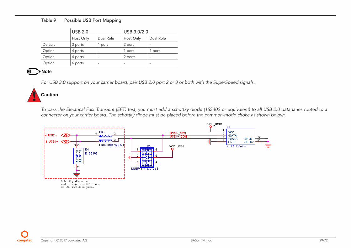
Caution
To pass the Electrical Fast Transient (EFT) test, you must add a schottky diode (1SS402 or equivalent) to all USB 2.0 data lanes routed to a connector on your carrier board. The schottky diode must be placed before the common-mode choke as shown below:
Copyright © 2017 congatec AG SA50m14.indd 30/72
5.6 SD Card
The conga-SA5 offers a 4-bit SD interface on the edge finger. The interface supports:
• SD Memory Card Specification 3.01
• SD 3.01 @ 1.8 V or @ 3.3 V signaling
• up to 200 MHz clock frequency
• up to 104 MBps data rates with four parallel data lines
• 1-bit and 4-bit transfer mode
• card insertion and removal detection
Note
The SD card interface supports only storage devices.
5.7 Audio (HDA / I2S)
The conga-SA5 offers the following audio interfaces:
• up to two I2S interfaces (I2S0 and I2S2)
• up to one HDA interface (shares pins with I2S2)
Note
The conga-SA5 does not support GPIO functionality on GPIO4 if HDA interface is implemented.
5.8 UART
The conga-SA5 provides four UART ports—two ports via the congatec board controller (without handshake signals) and two ports via the SoC.
Note
1. The UART ports do not support legacy mode operation.
2. The driver for the two UART ports routed from the cBC is available on the congatec website www.congatec.com. You cannot use the two UART ports from the SoC under Windows because Intel® does not provide the necessary driver. You can use them only under Linux.
Copyright © 2017 congatec AG SA50m14.indd 31/72
5.9 GPIO
The conga-SA5 offers five non-multiplexed GPIOs (port 7 - port 11) by default. The GPIOs are controlled by the congatec Board controller.
5.10 Communication Buses
The conga-SA5 offers the following communication buses:
• SPI
• I2C
• I2S
5.10.1 SPI
The conga-SA5 offers two SPI interfaces:
• eSPI/SPI1 for general purpose SPI devices
• SPI0 for on-module or carrier board flash device
5.10.2 I2C
The conga-SA5 offers two I2C interfaces:
• general purpose I2C
• power management I2C
These interfaces are implemented through the congatec board controller and accessed through the congatec CGOS driver and API. The controller provides a fast-mode multi-master I²C bus that has maximum I²C bandwidth.
5.10.3 I2S
The conga-SA5 offers two I2S interfaces:
• I2S0
• I2S2 (multiplexed with HDA signals for digital audio interfaces)
Copyright © 2017 congatec AG SA50m14.indd 32/72
5.11 Power Control
The conga-SA5 operates only with 5 V input voltage. Its power-up sequence is described below:
1. The 5 V input voltage (VDD_IN) supplied to the carrier board powers the conga-SA5.
2. The conga-SA5 enables its power circuits if the VIN_PWR_BAD# signal is high.
3. Depending on the carrier board design and configuration, the conga-SA5 detects a power button event (PWRBTN#) if implemented.
4. The conga-SA5 enables the carrier board power by asserting CARRIER_PWR_ON (SUS_S5#) and CARRIER_STBY# (SUS_S3#).
5. The conga-SA5 releases the RESET_OUT# and starts the boot process.
The power control signals are described below:
VIN_PWR_BAD#
When the VIN_PWR_BAD# signal (pin S150) is low, it indicates that the input voltage to the conga-SA5 is either not ready or out of specified range. Carrier board hardware should drive this signal low until the input power is up and stable. Releasing VIN_PWR_BAD# too early can cause numerous boot up problems.
CARRIER_PWR_ON
The CARRIER_PWR_ON signal (pin S154) is an active-high output signal. The module asserts this signal when all its power supplies are up, and subsequently enables the carrier board power supplies. This signal is equivalent to ACPI SUS_S5# signal.
CARRIER_STBY#
The CARRIER_STBY# signal (pin S153) is an active-low output that can be used to indicate that the conga-SA5 is going into suspend state, where only power management functions and system memory are powered.
The CARRIER_STBY# signal can also be used to disable the carrier board power that is not required during standby.
RESET_IN#
The RESET_IN# signal (pin P127) is an active-low open drain input signal from the carrier board. The signal may be used to force the module to reset or reboot.
Copyright © 2017 congatec AG SA50m14.indd 33/72
RESET_OUT#
The RESET_OUT# signal (pin P126) is an active-low output signal from the module. The module asserts this signal during the power-up sequencing to allow the carrier board power circuits to come up. The module deasserts this signal to begin the boot-up process.
POWER_BTN#
The POWER_BTN# (pin P128) is an active-low open drain power button input from the carrier board. This power button signal is used to wake up or shut down the system from S5 state (soft off).
Power Supply Implementation Guidelines
The operational power source for the conga-SA5 is 5 V. The remaining necessary voltages are internally generated on the module with onboard voltage regulators.
A carrier board designer should be aware of the important information below when designing a power supply for a conga-SA5 application:
• We have noticed that on some occasions, problems occur when using a 5V power supply that produces non monotonic voltage when powered up. The problem is that some internal circuits on the module (e.g. clock-generator chips) generate their own reset signals when the supply voltage exceeds a certain voltage threshold. A voltage dip after passing this threshold may lead to these circuits becoming confused, thereby resulting in a malfunction. This problem though rare, has been observed in some mobile power supply applications. The best way to ensure that this problem is not encountered is to observe the power supply rise waveform through an oscilloscope. This will help to determine if the rise is indeed monotonic and does not have any dips. You should do this during the power supply qualification phase to ensure that the problem does not occur in the application. For more information about this issue, visit www.formfactors.org and view page 25 figure 7 of the document “ATX12V Power Supply Design Guide V2.2”.
Inrush and Maximum Current Peaks on VDD_IN
The maximum peak-current on the conga-SA5 VDD_IN (5 V) power rail can be as high as 5 A for a maximum of 100 µs. You should therefore ensure the power supply and decoupling capacitors provide enough power to drive the module.
Note
For more information about power control event signals, refer to the SMARC® specification.
Copyright © 2017 congatec AG SA50m14.indd 34/72
6 Additional Features
6.1 Optional Onboard Interfaces
The conga-SA5 offers the following optional interfaces:
• Wi-fi/Bluetooth module
• TPM 2.0 connected via LPC bus
Note
The conga-SA5 variant with part number 050030 features both Wi-fi/Bluetooth and TPM modules onboard.
6.2 Standard Onboard Interfaces
The conga-SA5 offers the following standard interfaces:
• eMMC 5.0 (SSD) with up to 32 GB capacity
• Quad- or dual-channel low voltage memory (LPDDR4) with up to 2400 MTps and up to 8 GB capacity
• congatec board controller
6.2.1 congatec Board Controller (cBC)
The conga-SA5 is equipped with a Texas Instruments TI Stellaris microcontroller. The microcontroller plays an important role for most of the congatec BIOS features. By isolating some of the embedded features such as system monitoring or the I²C bus from the x86 core architecture, the microcontroller increases the performance and reliability of the BIOS features, even during low power mode. In addition, it ensures the congatec embedded feature set is compatible amongst all congatec modules.
Some of the features offered by the cBC are described below:
6.2.1.1 Board Information
The cBC provides a rich data-set of manufacturing and board information such as serial number, EAN number, hardware and firmware revisions, and so on. It also keeps track of dynamically changing data like runtime meter and boot counter.
Copyright © 2017 congatec AG SA50m14.indd 35/72
6.2.1.2 General Purpose Input/Output
The conga-SA5 offers general purpose inputs and outputs for custom system design. These GPIOs are controlled by the cBC.
6.2.1.3 Fan Control
The conga-SA5 has additional signals and functions to further improve system management. One of these signals is an output signal called PWMOUT that allows system fan control using a PWM (Pulse Width Modulation) output. Additionally, there is an input signal called TACHIN that provides the ability to monitor the system’s fan RPMs (revolutions per minute). This signal must receive two pulses per revolution in order to produce an accurate reading. For this reason, a two pulse per revolution fan or similar hardware solution is recommended.
Note
1. Use a four-wire fan to generate the correct speed readout.
2. For the correct fan control (PWMOUT, TACHIN) implementation, see the SMARC Design Guide Specification.
3. PWMOUT and TACHIN share their pins with GPIO 5 and 6 respectively. The conga-SA5 does not support fan control if these pins are used for GPIO functionality.
6.2.1.4 Power Loss Control
The cBC has full control of the power-up of the module and therefore can be used to specify the behavior of the system after an AC power loss condition. Supported modes are “Always On”, “Remain Off” and “Last State”.
6.2.1.5 Watchdog
The conga-SA5 is equipped with a multi stage watchdog solution that is triggered by software. The conga-SA5 does not support external hardware triggering because the SMARC Specification does not provide support for external hardware triggering of the watchdog.
For more information, see the application note AN3_Watchdog.pdf on the congatec AG website at www.congatec.com.
Note
The conga-SA5 module does not support the watchdog NMI mode.
Copyright © 2017 congatec AG SA50m14.indd 36/72
6.2.1.6 I2C Bus
The conga-SA5 supports I2C bus. See section 5.10.3 “I2C” for more information.
6.3 OEM BIOS Customization
The conga-SA5 is equipped with congatec Embedded BIOS, which is based on American Megatrends Inc. Aptio UEFI firmware. The congatec Embedded BIOS allows system designers to modify the BIOS. For more information about customizing the congatec Embedded BIOS, refer to the congatec System Utility user’s guide CGUTLm1x.pdf on the congatec website at www.congatec.com or contact technical support.
The customizable features are described below:
6.3.1 OEM Default Settings
This feature allows system designers to create and store their own BIOS default configuration. Customized BIOS development by congatec for OEM default settings is no longer necessary because customers can easily perform this configuration by themselves using the congatec system utility CGUTIL. See congatec application note AN8_Create_OEM_Default_Map.pdf on the congatec website for details on how to add OEM default settings to the congatec Embedded BIOS.
6.3.2 OEM Boot Logo
This feature allows system designers to replace the standard text output displayed during POST with their own BIOS boot logo. Customized BIOS development by congatec for OEM Boot Logo is no longer necessary because customers can easily perform this configuration by themselves using the congatec system utility CGUTIL. See congatec application note AN8_Create_And_Add_Bootlogo.pdf on the congatec website for details on how to add OEM boot logo to the congatec Embedded BIOS.
6.3.3 OEM POST Logo
This feature allows system designers to replace the congatec POST logo displayed in the upper left corner of the screen during BIOS POST with their own BIOS POST logo. Use the congatec system utility CGUTIL 1.5.4 or later to replace/add the OEM POST logo.
Copyright © 2017 congatec AG SA50m14.indd 37/72
6.3.4 OEM BIOS Code/Data
With the congatec embedded BIOS it is possible for system designers to add their own code to the BIOS POST process. The congatec Embedded BIOS first calls the OEM code before handing over control to the OS loader.
Note
The OEM BIOS code of the new UEFI based firmware is called only when the CSM (Compatibility Support Module) is enabled in the BIOS setup menu. For more information on how to add OEM code, contact congatec technical support.
6.3.5 OEM DXE Driver
This feature allows designers to add their own UEFI DXE driver to the congatec embedded BIOS. Contact congatec technical support for more information on how to add an OEM DXE driver.
6.4 congatec Battery Management Interface
To facilitate the development of battery powered mobile systems based on embedded modules, congatec AG defined an interface for the exchange of data between a CPU module (using an ACPI operating system) and a Smart Battery system. A system developed according to the congatec Battery Management Interface Specification can provide the battery management functions supported by an ACPI capable operating system (e.g. charge state of the battery, information about the battery, alarms/events for certain battery states, ...) without the need for any additional modifications to the system BIOS.
In addition to the ACPI-Compliant Control Method Battery mentioned above, the latest versions of the conga-SA5 BIOS and board controller firmware also support LTC1760 battery manager from Linear Technology and a battery only solution (no charger). All three battery solutions are supported on the I2C bus and the SMBus. This gives the system designer more flexibility when choosing the appropriate battery sub-system.
For more information about this subject visit the congatec website and view the following documents:
• congatec Battery Management Interface Specification
• Battery System Design Guide
• conga-SBM3 User’s Guide
Copyright © 2017 congatec AG SA50m14.indd 38/72
6.5 API Support (CGOS)
In order to benefit from the above mentioned non-industry standard feature set, congatec provides an API that allows application software developers to easily integrate all these features into their code. The CGOS API (congatec Operating System Application Programming Interface) is the congatec proprietary API that is available for all commonly used Operating Systems such as Win32, Win64, Win CE, Linux. The architecture of the CGOS API driver provides the ability to write application software that runs unmodified on all congatec CPU modules. All the hardware related code is contained within the congatec embedded BIOS on the module. See section 1.1 of the CGOS API software developers guide, which is available on the congatec website.
6.6 Suspend to Ram
The Suspend to RAM feature is available on the conga-SA5.
Copyright © 2017 congatec AG SA50m14.indd 39/72
7 conga Tech NotesThe conga-SA5 has some technological features that require additional explanation. The following section will give the reader a better understanding of some of these features. This information will also help to gain a better understanding of the information found in the system resources section of this user’s guide as well as some of the setup nodes found in the BIOS Setup Description section.
7.1 Intel® Apollo Lake SoC Features
7.1.1 Processor Core
The SoC features Dual or Quad Out-of-Order Execution processor cores. The cores are grouped into Dual-Core modules with each module sharing a 1 MB L2 cache (512 KB per core). Some of the features supported by the core are:
• Intel 64 architecture
• Intel Streaming SIMD Extensions
• Support for Intel VTx-2 and VT-d
• Thermal management support vial Intel Thermal Monitor
• Uses Power Aware Interrupt Routing
• Uses 14 nm process technology
Note
Intel Hyper-Threading technology is not supported (four cores execute four threads)
7.1.1.1 Intel Virtualization Technology
Intel® Virtualization Technology (Intel® VT) makes a single system appear as multiple independent systems to software. This allows multiple, independent operating systems to run simultaneously on a single system. Intel® VT comprises technology components to support virtualization of platforms based on Intel architecture microprocessors and chipsets. Intel® Virtualization Technology for IA-32, Intel® 64 and Intel® Architecture Intel® VT-x) added hardware support in the processor to improve the virtualization performance and robustness.
Note
congatec does not offer virtual machine monitor (VMM) software. All VMM software support questions and queries should be directed to the VMM software vendor and not congatec technical support.
Copyright © 2017 congatec AG SA50m14.indd 40/72
7.1.1.2 AHCI
The SoC provides hardware support for Advanced Host Controller Interface (AHCI), a programming interface for SATA host controllers. Platforms supporting AHCI may take advantage of performance features such as no master/slave designation for SATA devices (each device is treated as a master) and hardware-assisted native command queuing. AHCI also provides usability enhancements such as Hot-Plug.
7.1.1.3 Thermal Management
ACPI is responsible for allowing the operating system to play an important part in the system’s thermal management. This results in the operating system having the ability to take control of the operating environment by implementing cooling decisions according to the demands put on the CPU by the application.
The conga-SA5 ACPI thermal solution offers two different cooling policies.
• Passive Cooling
When the temperature in the thermal zone must be reduced, the operating system can decrease the power consumption of the processor by throttling the processor clock. One of the advantages of this cooling policy is that passive cooling devices (in this case the processor) do not produce any noise. Use the “passive cooling trip point” setup node in the BIOS setup program to determine the temperature threshold that the operating system will use to start or stop the passive cooling procedure.
• Critical Trip Point
If the temperature in the thermal zone reaches a critical point then the operating system will perform a system shut down in an orderly fashion in order to ensure that there is no damage done to the system as result of high temperatures. Use the “critical trip point” setup node in the BIOS setup program to determine the temperature threshold that the operating system will use to shut down the system.
Note
The end user must determine the cooling preferences for the system by using the setup nodes in the BIOS setup program to establish the appropriate trip points.
If passive cooling is activated and the processor temperature is above the trip point the processor clock is throttled. See section 12 of the ACPI Specification 2.0 C for more information about passive cooling.
Copyright © 2017 congatec AG SA50m14.indd 41/72
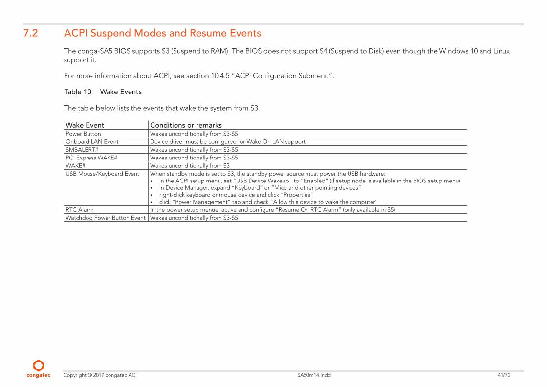
7.2 ACPI Suspend Modes and Resume Events
The conga-SA5 BIOS supports S3 (Suspend to RAM). The BIOS does not support S4 (Suspend to Disk) even though the Windows 10 and Linux support it.
For more information about ACPI, see section 10.4.5 “ACPI Configuration Submenu”.
Table 10 Wake Events
The table below lists the events that wake the system from S3.
Wake Event Conditions or remarksPower Button Wakes unconditionally from S3-S5Onboard LAN Event Device driver must be configured for Wake On LAN supportSMBALERT# Wakes unconditionally from S3-S5PCI Express WAKE# Wakes unconditionally from S3-S5WAKE# Wakes unconditionally from S3USB Mouse/Keyboard Event When standby mode is set to S3, the standby power source must power the USB hardware:
• in the ACPI setup menu, set “USB Device Wakeup” to “Enabled” (if setup node is available in the BIOS setup menu) • in Device Manager, expand “Keyboard” or “Mice and other pointing devices” • right-click keyboard or mouse device and click “Properties” • click “Power Management” tab and check “Allow this device to wake the computer’
RTC Alarm In the power setup menue, active and configure “Resume On RTC Alarm” (only available in S5)Watchdog Power Button Event Wakes unconditionally from S3-S5
Copyright © 2017 congatec AG SA50m14.indd 42/72
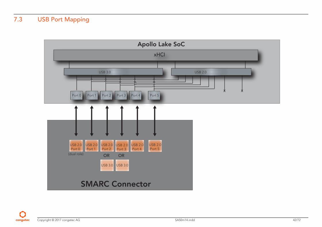
7.3 USB Port Mapping
USB 2.0Port 2
USB 3.0 USB 2.0
Port 1Port 0 Port 4 Port 5
SMARC Connector
Port 3Port 2
xHCI
USB 2.0Port 1
USB 2.0Port 0
(dual role)
Apollo Lake SoC
OR OR
USB 2.0Port 3
USB 3.0
USB 2.0Port 4
USB 2.0Port 5
x x
USB 3.0
Copyright © 2017 congatec AG SA50m14.indd 43/72
8 Signal Descriptions and Pinout TablesThe following section describes the signals found on SMARC® module’s edge fingers. The pinout of the module complies with SMARC Specification 2.0.
The table below describes the terminology used in this section. The PU/PD column indicates if a pull-up or pull-down resistor has been used. If the field entry area in this column for the signal is empty, then no pull-up or pull-down resistor has been implemented. The “#” symbol at the end of the signal name indicates that the active or asserted state occurs when the signal is at a low voltage level.
Note
Not all the signals described in this section are available on all conga-SA5 variants. Use the article number of the module and refer to the “conga-SA5 Options Information table” in section 1 to determine the options available on the module.
Table 11 Signal Tables Terminology Descriptions
Term DescriptionI Input to the module
O Output from the module
O OD Open drain output from the module
I OD Open drain input to the module, with pull-up on module
OD Open drain
I/O Bi-directional Input/Output Pin
PU(i)/PD(i) Pull-up or pull-down resistor internal to the SoC or transceiver
VDD_IN Signal may be exposed to module input voltage range (4.75 to 5.25V)
CMOS Logic input or output with 3.3 V signal level
GBe MDI Differential analog signaling for Gigabit Media Dependent Interface
LVDS DP LVDS signaling for DisplayPort devices
LVDS D-PHY LVDS signaling for MIPI CSI-2 camera and DSI display interfaces
LVDS LCD LVDS signaling for LVDS LCD displays
LVDS PCIE LVDS signaling for PCIe interfaces
LVDS SATA LVDS signaling for SATA interfaces
TMDS LVDS signaling for HDMI display interfaces
USB DC coupled differential signaling for traditional (non-Superspeed) USB signals
USB SS LVDS signaling for SuperSpeed USB signals
PCIE PCI Express differential pair signals. In compliance with the PCI Express Base Specification 2.0
USB VBUS 5V 5V tolerant input for USB VBUS detection
Copyright © 2017 congatec AG SA50m14.indd 44/72
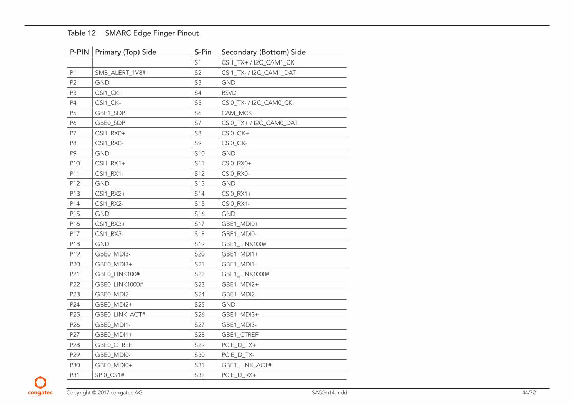
Table 12 SMARC Edge Finger Pinout
P-PIN Primary (Top) Side S-Pin Secondary (Bottom) SideS1 CSI1_TX+ / I2C_CAM1_CK
P1 SMB_ALERT_1V8# S2 CSI1_TX- / I2C_CAM1_DAT
P2 GND S3 GND
P3 CSI1_CK+ S4 RSVD
P4 CSI1_CK- S5 CSI0_TX- / I2C_CAM0_CK
P5 GBE1_SDP S6 CAM_MCK
P6 GBE0_SDP S7 CSI0_TX+ / I2C_CAM0_DAT
P7 CSI1_RX0+ S8 CSI0_CK+
P8 CSI1_RX0- S9 CSI0_CK-
P9 GND S10 GND
P10 CSI1_RX1+ S11 CSI0_RX0+
P11 CSI1_RX1- S12 CSI0_RX0-
P12 GND S13 GND
P13 CSI1_RX2+ S14 CSI0_RX1+
P14 CSI1_RX2- S15 CSI0_RX1-
P15 GND S16 GND
P16 CSI1_RX3+ S17 GBE1_MDI0+
P17 CSI1_RX3- S18 GBE1_MDI0-
P18 GND S19 GBE1_LINK100#
P19 GBE0_MDI3- S20 GBE1_MDI1+
P20 GBE0_MDI3+ S21 GBE1_MDI1-
P21 GBE0_LINK100# S22 GBE1_LINK1000#
P22 GBE0_LINK1000# S23 GBE1_MDI2+
P23 GBE0_MDI2- S24 GBE1_MDI2-
P24 GBE0_MDI2+ S25 GND
P25 GBE0_LINK_ACT# S26 GBE1_MDI3+
P26 GBE0_MDI1- S27 GBE1_MDI3-
P27 GBE0_MDI1+ S28 GBE1_CTREF
P28 GBE0_CTREF S29 PCIE_D_TX+
P29 GBE0_MDI0- S30 PCIE_D_TX-
P30 GBE0_MDI0+ S31 GBE1_LINK_ACT#
P31 SPI0_CS1# S32 PCIE_D_RX+
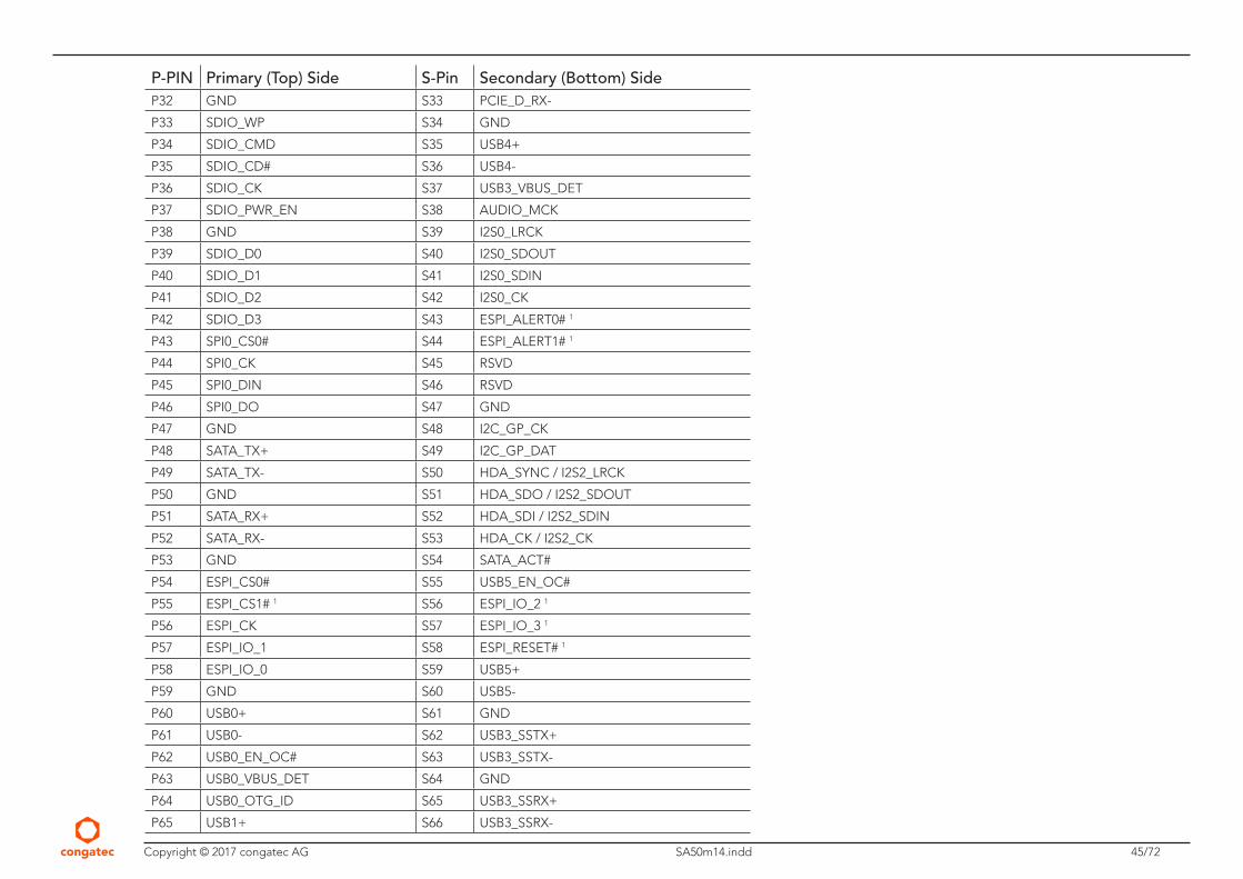
Copyright © 2017 congatec AG SA50m14.indd 45/72
P-PIN Primary (Top) Side S-Pin Secondary (Bottom) SideP32 GND S33 PCIE_D_RX-
P33 SDIO_WP S34 GND
P34 SDIO_CMD S35 USB4+
P35 SDIO_CD# S36 USB4-
P36 SDIO_CK S37 USB3_VBUS_DET
P37 SDIO_PWR_EN S38 AUDIO_MCK
P38 GND S39 I2S0_LRCK
P39 SDIO_D0 S40 I2S0_SDOUT
P40 SDIO_D1 S41 I2S0_SDIN
P41 SDIO_D2 S42 I2S0_CK
P42 SDIO_D3 S43 ESPI_ALERT0# 1
P43 SPI0_CS0# S44 ESPI_ALERT1# 1
P44 SPI0_CK S45 RSVD
P45 SPI0_DIN S46 RSVD
P46 SPI0_DO S47 GND
P47 GND S48 I2C_GP_CK
P48 SATA_TX+ S49 I2C_GP_DAT
P49 SATA_TX- S50 HDA_SYNC / I2S2_LRCK
P50 GND S51 HDA_SDO / I2S2_SDOUT
P51 SATA_RX+ S52 HDA_SDI / I2S2_SDIN
P52 SATA_RX- S53 HDA_CK / I2S2_CK
P53 GND S54 SATA_ACT#
P54 ESPI_CS0# S55 USB5_EN_OC#
P55 ESPI_CS1# 1 S56 ESPI_IO_2 1
P56 ESPI_CK S57 ESPI_IO_3 1
P57 ESPI_IO_1 S58 ESPI_RESET# 1
P58 ESPI_IO_0 S59 USB5+
P59 GND S60 USB5-
P60 USB0+ S61 GND
P61 USB0- S62 USB3_SSTX+
P62 USB0_EN_OC# S63 USB3_SSTX-
P63 USB0_VBUS_DET S64 GND
P64 USB0_OTG_ID S65 USB3_SSRX+
P65 USB1+ S66 USB3_SSRX-
Copyright © 2017 congatec AG SA50m14.indd 46/72
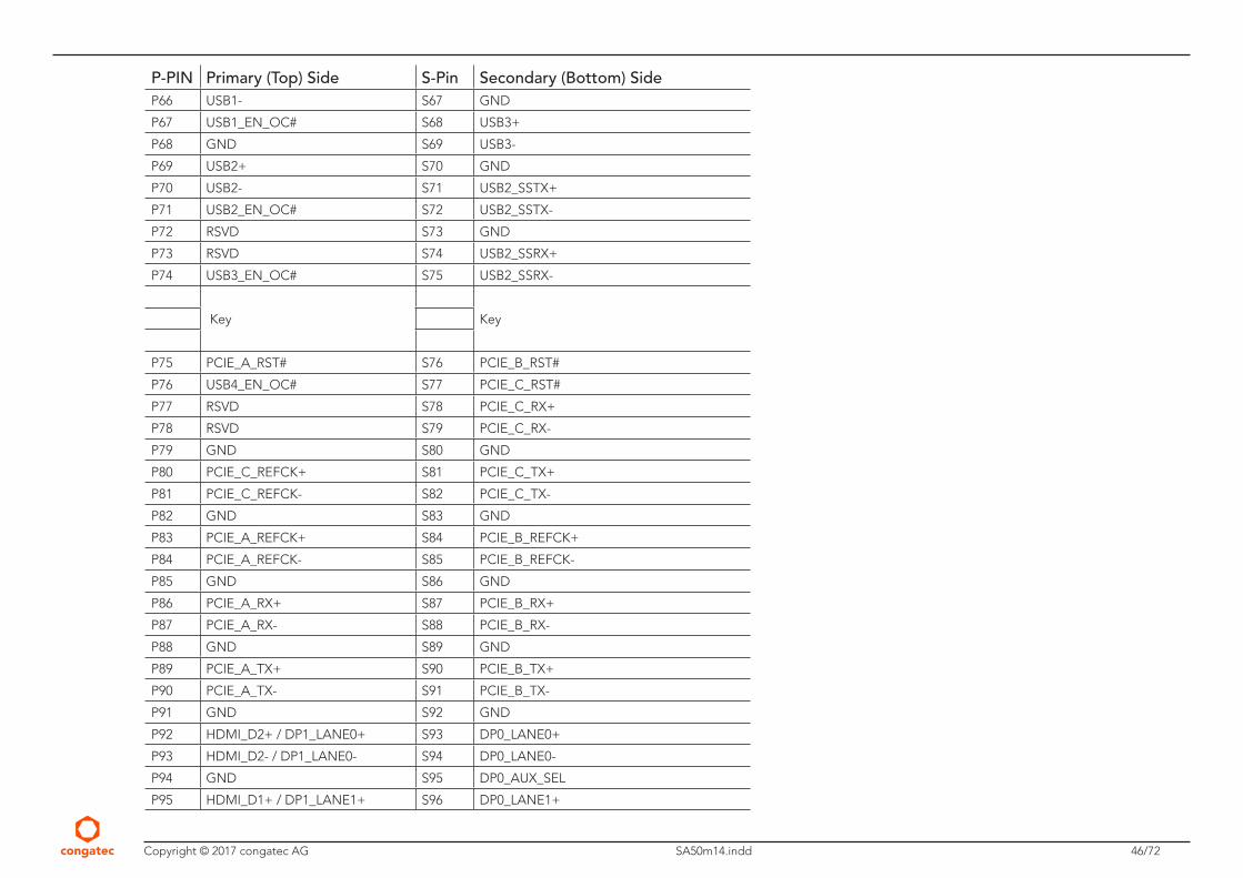
P-PIN Primary (Top) Side S-Pin Secondary (Bottom) SideP66 USB1- S67 GND
P67 USB1_EN_OC# S68 USB3+
P68 GND S69 USB3-
P69 USB2+ S70 GND
P70 USB2- S71 USB2_SSTX+
P71 USB2_EN_OC# S72 USB2_SSTX-
P72 RSVD S73 GND
P73 RSVD S74 USB2_SSRX+
P74 USB3_EN_OC# S75 USB2_SSRX-
Key Key
P75 PCIE_A_RST# S76 PCIE_B_RST#
P76 USB4_EN_OC# S77 PCIE_C_RST#
P77 RSVD S78 PCIE_C_RX+
P78 RSVD S79 PCIE_C_RX-
P79 GND S80 GND
P80 PCIE_C_REFCK+ S81 PCIE_C_TX+
P81 PCIE_C_REFCK- S82 PCIE_C_TX-
P82 GND S83 GND
P83 PCIE_A_REFCK+ S84 PCIE_B_REFCK+
P84 PCIE_A_REFCK- S85 PCIE_B_REFCK-
P85 GND S86 GND
P86 PCIE_A_RX+ S87 PCIE_B_RX+
P87 PCIE_A_RX- S88 PCIE_B_RX-
P88 GND S89 GND
P89 PCIE_A_TX+ S90 PCIE_B_TX+
P90 PCIE_A_TX- S91 PCIE_B_TX-
P91 GND S92 GND
P92 HDMI_D2+ / DP1_LANE0+ S93 DP0_LANE0+
P93 HDMI_D2- / DP1_LANE0- S94 DP0_LANE0-
P94 GND S95 DP0_AUX_SEL
P95 HDMI_D1+ / DP1_LANE1+ S96 DP0_LANE1+
Copyright © 2017 congatec AG SA50m14.indd 47/72
P-PIN Primary (Top) Side S-Pin Secondary (Bottom) SideP96 HDMI_D1- / DP1_LANE1- S97 DP0_LANE1-
P97 GND S98 DP0_HPD
P98 HDMI_D0+ / DP1_LANE2+ S99 DP0_LANE2+
P99 HDMI_D0- / DP1_LANE2- S100 DP0_LANE2-
P100 GND S101 GND
P101 HDMI_CK+ / DP1_LANE3+ S102 DP0_LANE3+
P102 HDMI_CK- / DP1_LANE3- S103 DP0_LANE3-
P103 GND S104 USB3_OTG_ID
P104 HDMI_HPD / DP1_HPD S105 DP0_AUX+
P105 HDMI_CTRL_CK / DP1_AUX+ S106 DP0_AUX-
P106 HDMI_CTRL_DAT / DP1_AUX- S107 LCD1_BKLT_EN
P107 DP1_AUX_SEL S108 LVDS1_CK+ / eDP1_AUX+ / DSI1_CLK+
P108 GPIO0 / CAM0_PWR# S109 LVDS1_CK- / eDP1_AUX- / DSI1_CLK-
P109 GPIO1 / CAM1_PWR# S110 GND
P110 GPIO2 / CAM0_RST# S111 LVDS1_0+ / eDP1_TX0+ / DSI1_D0+
P111 GPIO3 / CAM1_RST# S112 LVDS1_0- / eDP1_TX0- / DSI1_D0-
P112 GPIO4 / HDA_RST# S113 eDP1_HPD / DSI1_TE
P113 GPIO5 / PWM_OUT S114 LVDS1_1+ / eDP1_TX1+ / DSI1_D1+
P114 GPIO6 / TACHIN S115 LVDS1_1- / eDP1_TX1- / DSI1_D1-
P115 GPIO7 S116 LCD1_VDD_EN
P116 GPIO8 S117 LVDS1_2+ / eDP1_TX2+ / DSI1_D2+
P117 GPIO9 S118 LVDS1_2- / eDP1_TX2- / DSI1_D2-
P118 GPIO10 S119 GND
P119 GPIO11 S120 LVDS1_3+ / eDP1_TX3+ / DSI1_D3+
P120 GND S121 LVDS1_3- / eDP1_TX3- / DSI1_D3-
P121 I2C_PM_CK S122 LCD1_BKLT_PWM
P122 I2C_PM_DAT S123 RSVD
P123 BOOT_SEL0# S124 GND
P124 BOOT_SEL1# S125 LVDS0_0+ / eDP0_TX0+ / DSI0_D0+
P125 BOOT_SEL2# S126 LVDS0_0- / eDP0_TX0- / DSI0_D0-
P126 RESET_OUT# S127 LCD0_BKLT_EN
P127 RESET_IN# S128 LVDS0_1+ / eDP0_TX1+ / DSI0_D1+
P128 POWER_BTN# S129 LVDS0_1- / eDP0_TX1- / DSI0_D1-
Copyright © 2017 congatec AG SA50m14.indd 48/72
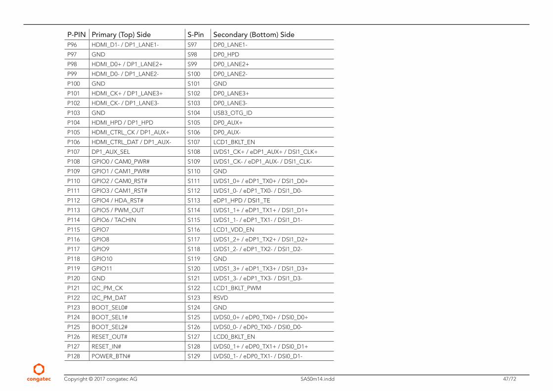
P-PIN Primary (Top) Side S-Pin Secondary (Bottom) SideP129 SER0_TX S130 GND
P130 SER0_RX S131 LVDS0_2+ / eDP0_TX2+ / DSI0_D2+
P131 SER0_RTS# S132 LVDS0_2- / eDP0_TX2- / DSI0_D2-
P132 SER0_CTS# S133 LCD0_VDD_EN
P133 GND S134 LVDS0_CK+ / eDP0_AUX+ / DSI0_CLK+
P134 SER1_TX S135 LVDS0_CK- / eDP0_AUX- / DSI0_CLK-
P135 SER1_RX S136 GND
P136 SER2_TX S137 LVDS0_3+ / eDP0_TX3+ / DSI0_D3+
P137 SER2_RX S138 LVDS0_3- / eDP0_TX3- / DSI0_D3-
P138 SER2_RTS# S139 I2C_LCD_CK
P139 SER2_CTS# S140 I2C_LCD_DAT
P140 SER3_TX S141 LCD0_BKLT_PWM
P141 SER3_RX S142 RSVD
P142 GND S143 GND
P143 CAN0_TX 1 S144 eDP0_HPD / DSI0_TE
P144 CAN0_RX 1 S145 WDT_TIME_OUT#
P145 CAN1_TX 1 S146 PCIE_WAKE#
P146 CAN1_RX 1 S147 VDD_RTC
P147 VDD_IN S148 LID#
P148 VDD_IN S149 SLEEP#
P149 VDD_IN S150 VIN_PWR_BAD#
P150 VDD_IN S151 CHARGING#
P151 VDD_IN S152 CHARGER_PRSNT#
P152 VDD_IN S153 CARRIER_STBY#
P153 VDD_IN S154 CARRIER_PWR_ON
P154 VDD_IN S155 FORCE_RECOV#
P155 VDD_IN S156 BATLOW#
P156 VDD_IN S157 TEST#
S158 GND
Note
1. Not supported on conga-SA5.
Copyright © 2017 congatec AG SA50m14.indd 49/72
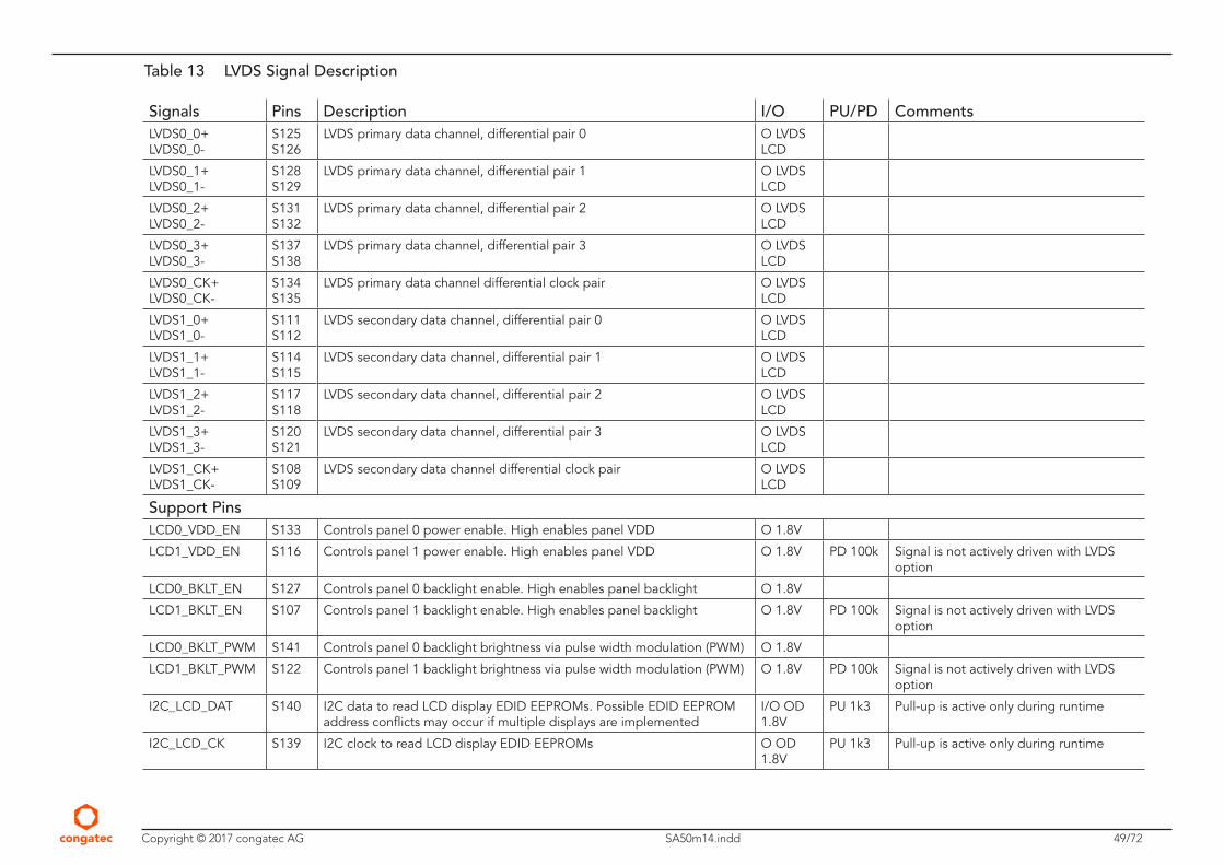
Table 13 LVDS Signal Description
Signals Pins Description I/O PU/PD CommentsLVDS0_0+LVDS0_0-
S125S126
LVDS primary data channel, differential pair 0 O LVDS LCD
LVDS0_1+ LVDS0_1-
S128S129
LVDS primary data channel, differential pair 1 O LVDS LCD
LVDS0_2+ LVDS0_2-
S131S132
LVDS primary data channel, differential pair 2 O LVDS LCD
LVDS0_3+ LVDS0_3-
S137S138
LVDS primary data channel, differential pair 3 O LVDS LCD
LVDS0_CK+LVDS0_CK-
S134S135
LVDS primary data channel differential clock pair O LVDS LCD
LVDS1_0+ LVDS1_0-
S111S112
LVDS secondary data channel, differential pair 0 O LVDS LCD
LVDS1_1+ LVDS1_1-
S114S115
LVDS secondary data channel, differential pair 1 O LVDS LCD
LVDS1_2+ LVDS1_2-
S117S118
LVDS secondary data channel, differential pair 2 O LVDS LCD
LVDS1_3+ LVDS1_3-
S120S121
LVDS secondary data channel, differential pair 3 O LVDS LCD
LVDS1_CK+ LVDS1_CK-
S108S109
LVDS secondary data channel differential clock pair O LVDS LCD
Support PinsLCD0_VDD_EN S133 Controls panel 0 power enable. High enables panel VDD O 1.8V
LCD1_VDD_EN S116 Controls panel 1 power enable. High enables panel VDD O 1.8V PD 100k Signal is not actively driven with LVDS option
LCD0_BKLT_EN S127 Controls panel 0 backlight enable. High enables panel backlight O 1.8V
LCD1_BKLT_EN S107 Controls panel 1 backlight enable. High enables panel backlight O 1.8V PD 100k Signal is not actively driven with LVDS option
LCD0_BKLT_PWM S141 Controls panel 0 backlight brightness via pulse width modulation (PWM) O 1.8V
LCD1_BKLT_PWM S122 Controls panel 1 backlight brightness via pulse width modulation (PWM) O 1.8V PD 100k Signal is not actively driven with LVDS option
I2C_LCD_DAT S140 I2C data to read LCD display EDID EEPROMs. Possible EDID EEPROM address conflicts may occur if multiple displays are implemented
I/O OD 1.8V
PU 1k3 Pull-up is active only during runtime
I2C_LCD_CK S139 I2C clock to read LCD display EDID EEPROMs O OD 1.8V
PU 1k3 Pull-up is active only during runtime
Copyright © 2017 congatec AG SA50m14.indd 50/72
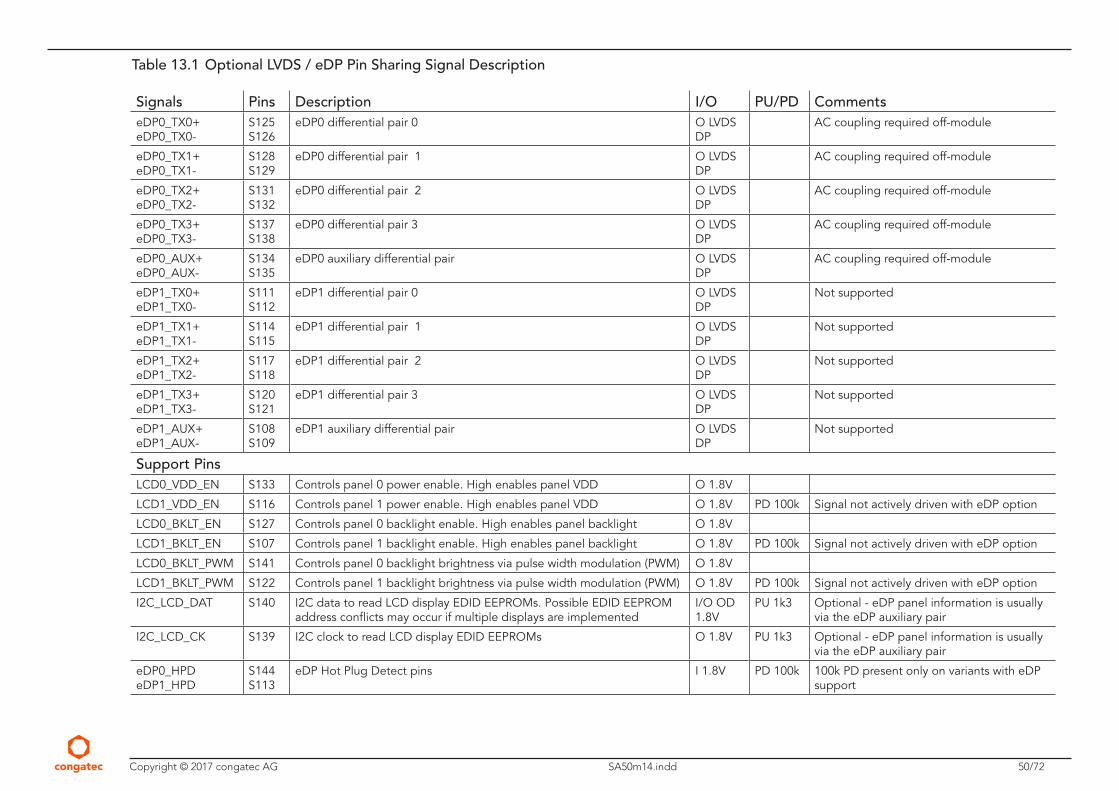
Table 13.1 Optional LVDS / eDP Pin Sharing Signal Description
Signals Pins Description I/O PU/PD CommentseDP0_TX0+ eDP0_TX0-
S125S126
eDP0 differential pair 0 O LVDS DP
AC coupling required off-module
eDP0_TX1+ eDP0_TX1-
S128S129
eDP0 differential pair 1 O LVDS DP
AC coupling required off-module
eDP0_TX2+ eDP0_TX2-
S131S132
eDP0 differential pair 2 O LVDS DP
AC coupling required off-module
eDP0_TX3+ eDP0_TX3-
S137S138
eDP0 differential pair 3 O LVDS DP
AC coupling required off-module
eDP0_AUX+ eDP0_AUX-
S134S135
eDP0 auxiliary differential pair O LVDS DP
AC coupling required off-module
eDP1_TX0+ eDP1_TX0-
S111S112
eDP1 differential pair 0 O LVDS DP
Not supported
eDP1_TX1+ eDP1_TX1-
S114S115
eDP1 differential pair 1 O LVDS DP
Not supported
eDP1_TX2+ eDP1_TX2-
S117S118
eDP1 differential pair 2 O LVDS DP
Not supported
eDP1_TX3+ eDP1_TX3-
S120S121
eDP1 differential pair 3 O LVDS DP
Not supported
eDP1_AUX+ eDP1_AUX-
S108S109
eDP1 auxiliary differential pair O LVDS DP
Not supported
Support PinsLCD0_VDD_EN S133 Controls panel 0 power enable. High enables panel VDD O 1.8V
LCD1_VDD_EN S116 Controls panel 1 power enable. High enables panel VDD O 1.8V PD 100k Signal not actively driven with eDP option
LCD0_BKLT_EN S127 Controls panel 0 backlight enable. High enables panel backlight O 1.8V
LCD1_BKLT_EN S107 Controls panel 1 backlight enable. High enables panel backlight O 1.8V PD 100k Signal not actively driven with eDP option
LCD0_BKLT_PWM S141 Controls panel 0 backlight brightness via pulse width modulation (PWM) O 1.8V
LCD1_BKLT_PWM S122 Controls panel 1 backlight brightness via pulse width modulation (PWM) O 1.8V PD 100k Signal not actively driven with eDP option
I2C_LCD_DAT S140 I2C data to read LCD display EDID EEPROMs. Possible EDID EEPROM address conflicts may occur if multiple displays are implemented
I/O OD 1.8V
PU 1k3 Optional - eDP panel information is usually via the eDP auxiliary pair
I2C_LCD_CK S139 I2C clock to read LCD display EDID EEPROMs O 1.8V PU 1k3 Optional - eDP panel information is usually via the eDP auxiliary pair
eDP0_HPDeDP1_HPD
S144S113
eDP Hot Plug Detect pins I 1.8V PD 100k 100k PD present only on variants with eDP support
Copyright © 2017 congatec AG SA50m14.indd 51/72
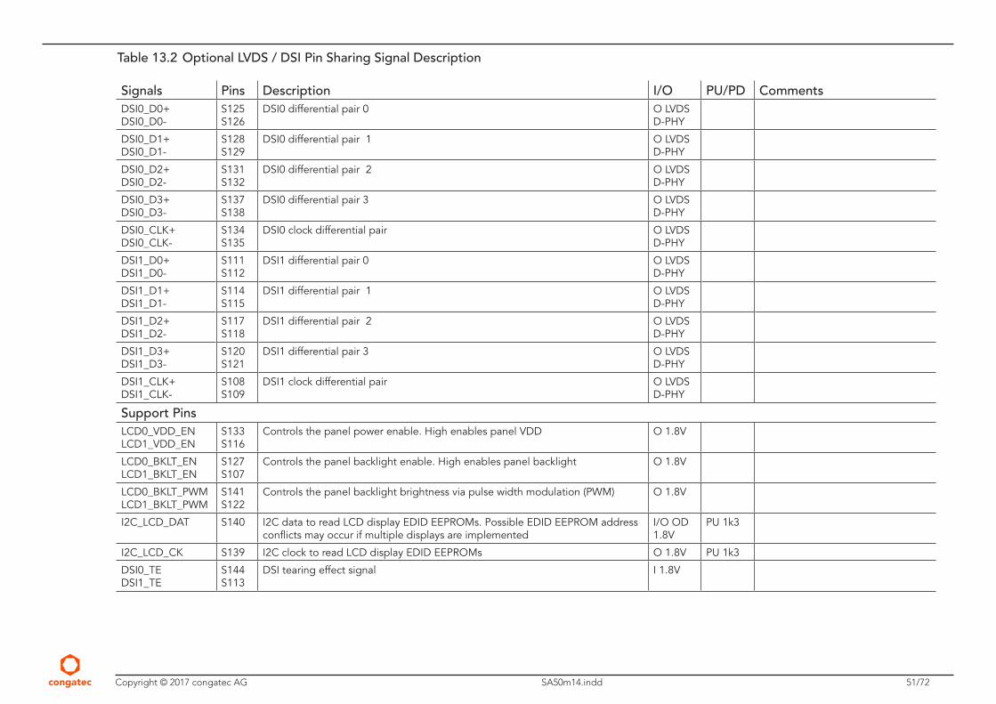
Table 13.2 Optional LVDS / DSI Pin Sharing Signal Description
Signals Pins Description I/O PU/PD CommentsDSI0_D0+ DSI0_D0-
S125S126
DSI0 differential pair 0 O LVDS D-PHY
DSI0_D1+ DSI0_D1-
S128S129
DSI0 differential pair 1 O LVDS D-PHY
DSI0_D2+ DSI0_D2-
S131S132
DSI0 differential pair 2 O LVDS D-PHY
DSI0_D3+ DSI0_D3-
S137S138
DSI0 differential pair 3 O LVDS D-PHY
DSI0_CLK+ DSI0_CLK-
S134S135
DSI0 clock differential pair O LVDS D-PHY
DSI1_D0+ DSI1_D0-
S111S112
DSI1 differential pair 0 O LVDS D-PHY
DSI1_D1+ DSI1_D1-
S114S115
DSI1 differential pair 1 O LVDS D-PHY
DSI1_D2+ DSI1_D2-
S117S118
DSI1 differential pair 2 O LVDS D-PHY
DSI1_D3+ DSI1_D3-
S120S121
DSI1 differential pair 3 O LVDS D-PHY
DSI1_CLK+DSI1_CLK-
S108S109
DSI1 clock differential pair O LVDS D-PHY
Support PinsLCD0_VDD_ENLCD1_VDD_EN
S133S116
Controls the panel power enable. High enables panel VDD O 1.8V
LCD0_BKLT_ENLCD1_BKLT_EN
S127S107
Controls the panel backlight enable. High enables panel backlight O 1.8V
LCD0_BKLT_PWMLCD1_BKLT_PWM
S141S122
Controls the panel backlight brightness via pulse width modulation (PWM) O 1.8V
I2C_LCD_DAT S140 I2C data to read LCD display EDID EEPROMs. Possible EDID EEPROM address conflicts may occur if multiple displays are implemented
I/O OD 1.8V
PU 1k3
I2C_LCD_CK S139 I2C clock to read LCD display EDID EEPROMs O 1.8V PU 1k3
DSI0_TEDSI1_TE
S144S113
DSI tearing effect signal I 1.8V
Copyright © 2017 congatec AG SA50m14.indd 52/72
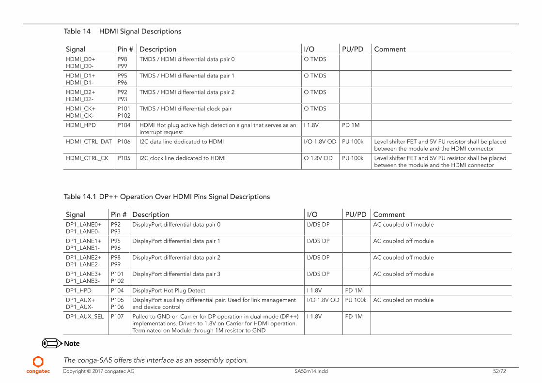
Table 14 HDMI Signal Descriptions
Signal Pin # Description I/O PU/PD CommentHDMI_D0+HDMI_D0-
P98P99
TMDS / HDMI differential data pair 0 O TMDS
HDMI_D1+HDMI_D1-
P95P96
TMDS / HDMI differential data pair 1 O TMDS
HDMI_D2+HDMI_D2-
P92P93
TMDS / HDMI differential data pair 2 O TMDS
HDMI_CK+HDMI_CK-
P101P102
TMDS / HDMI differential clock pair O TMDS
HDMI_HPD P104 HDMI Hot plug active high detection signal that serves as an interrupt request
I 1.8V PD 1M
HDMI_CTRL_DAT P106 I2C data line dedicated to HDMI I/O 1.8V OD PU 100k Level shifter FET and 5V PU resistor shall be placed between the module and the HDMI connector
HDMI_CTRL_CK P105 I2C clock line dedicated to HDMI O 1.8V OD PU 100k Level shifter FET and 5V PU resistor shall be placed between the module and the HDMI connector
Table 14.1 DP++ Operation Over HDMI Pins Signal Descriptions
Signal Pin # Description I/O PU/PD CommentDP1_LANE0+DP1_LANE0-
P92P93
DisplayPort differential data pair 0 LVDS DP AC coupled off module
DP1_LANE1+DP1_LANE1-
P95P96
DisplayPort differential data pair 1 LVDS DP AC coupled off module
DP1_LANE2+DP1_LANE2-
P98P99
DisplayPort differential data pair 2 LVDS DP AC coupled off module
DP1_LANE3+DP1_LANE3-
P101P102
DisplayPort differential data pair 3 LVDS DP AC coupled off module
DP1_HPD P104 DisplayPort Hot Plug Detect I 1.8V PD 1M
DP1_AUX+DP1_AUX-
P105P106
DisplayPort auxiliary differential pair. Used for link management and device control
I/O 1.8V OD PU 100k AC coupled on module
DP1_AUX_SEL P107 Pulled to GND on Carrier for DP operation in dual-mode (DP++) implementations. Driven to 1.8V on Carrier for HDMI operation. Terminated on Module through 1M resistor to GND
I 1.8V PD 1M
Note
The conga-SA5 offers this interface as an assembly option.
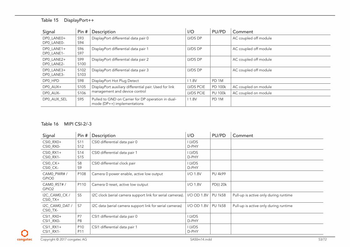
Copyright © 2017 congatec AG SA50m14.indd 53/72
Table 15 DisplayPort++
Signal Pin # Description I/O PU/PD CommentDP0_LANE0+DP0_LANE0-
S93S94
DisplayPort differential data pair 0 LVDS DP AC coupled off module
DP0_LANE1+DP0_LANE1-
S96S97
DisplayPort differential data pair 1 LVDS DP AC coupled off module
DP0_LANE2+DP0_LANE2-
S99S100
DisplayPort differential data pair 2 LVDS DP AC coupled off module
DP0_LANE3+DP0_LANE3-
S102S103
DisplayPort differential data pair 3 LVDS DP AC coupled off module
DP0_HPD S98 DisplayPort Hot Plug Detect I 1.8V PD 1M
DP0_AUX+ S105 DisplayPort auxiliary differential pair. Used for link management and device control
LVDS PCIE PD 100k AC coupled on module
DP0_AUX- S106 LVDS PCIE PU 100k AC coupled on module
DP0_AUX_SEL S95 Pulled to GND on Carrier for DP operation in dual-mode (DP++) implementations
I 1.8V PD 1M
Table 16 MIPI CSI-2/-3
Signal Pin # Description I/O PU/PD CommentCSI0_RX0+CSI0_RX0-
S11S12
CSI0 differential data pair 0 I LVDS D-PHY
CSI0_RX1+CSI0_RX1-
S14S15
CSI0 differential data pair 1 I LVDS D-PHY
CSI0_CK+CSI0_CK-
S8S9
CSI0 differential clock pair I LVDS D-PHY
CAM0_PWR# / GPIO0
P108 Camera 0 power enable, active low output I/O 1.8V PU 4k99
CAM0_RST# / GPIO2
P110 Camera 0 reset, active low output I/O 1.8V PD(i) 20k
I2C_CAM0_CK /CSI0_TX+
S5 I2C clock (serial camera support link for serial cameras). I/O OD 1.8V PU 1k58 Pull-up is active only during runtime
I2C_CAM0_DAT /CSI0_TX-
S7 I2C data (serial camera support link for serial cameras) I/O OD 1.8V PU 1k58 Pull-up is active only during runtime
CSI1_RX0+CSI1_RX0-
P7P8
CSI1 differential data pair 0 I LVDS D-PHY
CSI1_RX1+CSI1_RX1-
P10P11
CSI1 differential data pair 1 I LVDS D-PHY
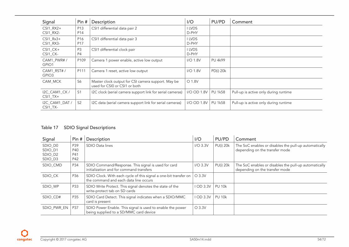
Copyright © 2017 congatec AG SA50m14.indd 54/72
Signal Pin # Description I/O PU/PD CommentCSI1_RX2+CSI1_RX2-
P13P14
CSI1 differential data pair 2 I LVDS D-PHY
CSI1_Rx3+CSI1_RX3-
P16P17
CSI1 differential data pair 3 I LVDS D-PHY
CSI1_CK+CSI1_CK-
P3P4
CSI1 differential clock pair I LVDS D-PHY
CAM1_PWR# / GPIO1
P109 Camera 1 power enable, active low output I/O 1.8V PU 4k99
CAM1_RST# / GPIO3
P111 Camera 1 reset, active low output I/O 1.8V PD(i) 20k
CAM_MCK S6 Master clock output for CSI camera support. May be used for CSI0 or CSI1 or both
O 1.8V
I2C_CAM1_CK /CSI1_TX+
S1 I2C clock (serial camera support link for serial cameras) I/O OD 1.8V PU 1k58 Pull-up is active only during runtime
I2C_CAM1_DAT / CSI1_TX-
S2 I2C data (serial camera support link for serial cameras) I/O OD 1.8V PU 1k58 Pull-up is active only during runtime
Table 17 SDIO Signal Descriptions
Signal Pin # Description I/O PU/PD CommentSDIO_D0SDIO_D1SDIO_D2SDIO_D3
P39P40P41P42
SDIO Data lines I/O 3.3V PU(i) 20k The SoC enables or disables the pull-up automatically depending on the transfer mode
SDIO_CMD P34 SDIO Command/Response. This signal is used for card initialization and for command transfers
I/O 3.3V PU(i) 20k The SoC enables or disables the pull-up automatically depending on the transfer mode
SDIO_CK P36 SDIO Clock. With each cycle of this signal a one-bit transfer on the command and each data line occurs
O 3.3V
SDIO_WP P33 SDIO Write Protect. This signal denotes the state of the write-protect tab on SD cards
I OD 3.3V PU 10k
SDIO_CD# P35 SDIO Card Detect. This signal indicates when a SDIO/MMC card is present
I OD 3.3V PU 10k
SDIO_PWR_EN P37 SDIO Power Enable. This signal is used to enable the power being supplied to a SD/MMC card device
O 3.3V
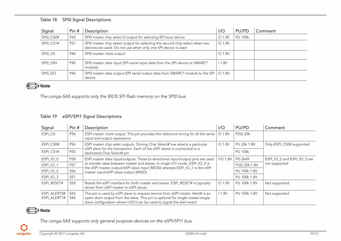
Copyright © 2017 congatec AG SA50m14.indd 55/72
Table 18 SPI0 Signal Descriptions
Signal Pin # Description I/O PU/PD CommentSPI0_CS0# P43 SPI0 master chip select 0 output for selecting SPI boot device O 1.8V PU 100k
SPI0_CS1# P31 SPI0 master chip select output for selecting the second chip select when two devices are used. Do not use when only one SPI device is used
O 1.8V
SPI0_CK P44 SPI0 master clock output O 1.8V
SPI0_DIN P45 SPI0 master data input (SPI serial input data from the SPI device to SMARC® module)
I 1.8V
SPI0_DO P46 SPI0 master data output (SPI serial output data from SMARC® module to the SPI device
O 1.8V
Note
The conga-SA5 supports only the BIOS SPI flash memory on the SPI0 bus.
Table 19 eSPI/SPI1 Signal Descriptions
Signal Pin # Description I/O PU/PD CommentESPI_CK P56 ESPI master clock output. This pin provides the reference timing for all the serial
input and output operationsO 1.8V PD(i) 20k
ESPI_CS0# P54 ESPI master chip selet outputs. Driving Chip Select# low selects a particular eSPI slave for the transaction. Each of the eSPI slaves is connected to a dedicated Chip Select# pin
O 1.8V PU 20k 1.8V Only ESPI_CS0# supported
ESPI_CS1# P55 PU 100k
ESPI_IO_0 P58 ESPI master data input/outputs. These bi-directional input/output pins are used to transfer data between master and slaves. In single I/O mode, ESPI_IO_0 is the eSPI master output/eSPI slave input (MOSI) whereas ESPI_IO_1 is the eSPI master input/eSPI slave output (MISO)
I/O 1.8V PD 2k49 ESPI_IO_2 and ESPI_IO_3 are not supportedESPI_IO_1 P57 PU(i) 20k 1.8V
ESPI_IO_2 S56 PU 100k 1.8V
ESPI_IO_3 S57 PU 100k 1.8V
ESPI_RESET# S58 Resets the eSPI interface for both master and slaves. ESPI_RESET# is typically driven from eSPI master to eSPI slaves
O 1.8V PU 100k 1.8V Not supported
ESPI_ALERT0#ESPI_ALERT1#
S43S44
This pin is used by eSPI slave to request service from eSPI master. Alert# is an open-drain output from the slave. This pin is optional for single master-single slave configuration where I/O[1] can be used to signal the alert event
I 1.8V PU 100k 1.8V Not supported
Note
The conga-SA5 supports only general purpose devices on the eSPI/SPI1 bus.
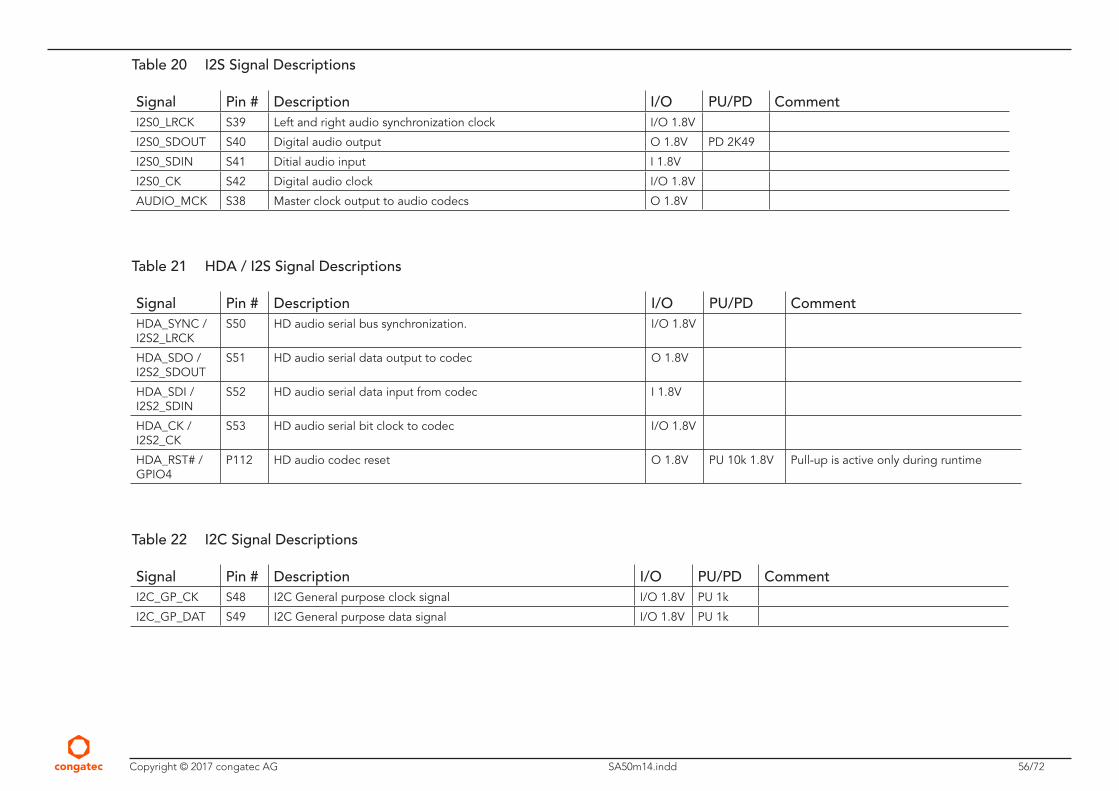
Copyright © 2017 congatec AG SA50m14.indd 56/72
Table 20 I2S Signal Descriptions
Signal Pin # Description I/O PU/PD CommentI2S0_LRCK S39 Left and right audio synchronization clock I/O 1.8V
I2S0_SDOUT S40 Digital audio output O 1.8V PD 2K49
I2S0_SDIN S41 Ditial audio input I 1.8V
I2S0_CK S42 Digital audio clock I/O 1.8V
AUDIO_MCK S38 Master clock output to audio codecs O 1.8V
Table 21 HDA / I2S Signal Descriptions
Signal Pin # Description I/O PU/PD CommentHDA_SYNC /I2S2_LRCK
S50 HD audio serial bus synchronization. I/O 1.8V
HDA_SDO /I2S2_SDOUT
S51 HD audio serial data output to codec O 1.8V
HDA_SDI /I2S2_SDIN
S52 HD audio serial data input from codec I 1.8V
HDA_CK /I2S2_CK
S53 HD audio serial bit clock to codec I/O 1.8V
HDA_RST# /GPIO4
P112 HD audio codec reset O 1.8V PU 10k 1.8V Pull-up is active only during runtime
Table 22 I2C Signal Descriptions
Signal Pin # Description I/O PU/PD CommentI2C_GP_CK S48 I2C General purpose clock signal I/O 1.8V PU 1k
I2C_GP_DAT S49 I2C General purpose data signal I/O 1.8V PU 1k
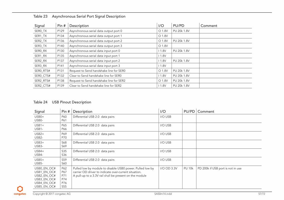
Copyright © 2017 congatec AG SA50m14.indd 57/72
Table 23 Asynchronous Serial Port Signal Description
Signal Pin # Description I/O PU/PD CommentSER0_TX P129 Asynchronous serial data output port 0 O 1.8V PU 20k 1.8V
SER1_TX P134 Asynchronous serial data output port 1 O 1.8V
SER2_TX P136 Asynchronous serial data output port 2 O 1.8V PU 20k 1.8V
SER3_TX P140 Asynchronous serial data output port 3 O 1.8V
SER0_RX P130 Asynchronous serial data input port 0 I 1.8V PU 20k 1.8V
SER1_RX P135 Asynchronous serial data input port 1 I 1.8V
SER2_RX P137 Asynchronous serial data input port 2 I 1.8V PU 20k 1.8V
SER3_RX P141 Asynchronous serial data input port 3 I 1.8V
SER0_RTS# P131 Request to Send handshake line for SER0 O 1.8V PU 20k 1.8V
SER0_CTS# P132 Clear to Send handshake line for SER0 I 1.8V PU 20k 1.8V
SER2_RTS# P138 Request to Send handshake line for SER2 O 1.8V PU 20k 1.8V
SER2_CTS# P139 Clear to Send handshake line for SER2 I 1.8V PU 20k 1.8V
Table 24 USB Pinout Description
Signal Pin # Description I/O PU/PD CommentUSB0+USB0-
P60P61
Differential USB 2.0 data pairs I/O USB
USB1+USB1-
P65P66
Differential USB 2.0 data pairs I/O USB
USB2+USB2-
P69P70
Differential USB 2.0 data pairs I/O USB
USB3+USB3-
S68S69
Differential USB 2.0 data pairs I/O USB
USB4+USB4-
S35S36
Differential USB 2.0 data pairs I/O USB
USB5+USB5-
S59S60
Differential USB 2.0 data pairs I/O USB
USB0_EN_OC#USB1_EN_OC#USB2_EN_OC#USB3_EN_OC#USB4_EN_OC#USB5_EN_OC#
P62P67P71P74P76S55
Pulled low by module to disable USB0 power. Pulled low by carrier OD driver to indicate over-current situation.A pull-up to a 3.3V rail shall be present on the module
I/O OD 3.3V PU 10k PD 200k if USB port is not in use
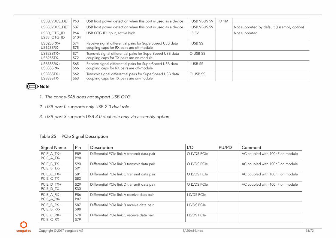
Copyright © 2017 congatec AG SA50m14.indd 58/72
USB0_VBUS_DET P63 USB host power detection when this port is used as a device I USB VBUS 5V PD 1M
USB3_VBUS_DET S37 USB host power detection when this port is used as a device I USB VBUS 5V Not supported by default (assembly option)
USB0_OTG_ID USB3_OTG_ID
P64S104
USB OTG ID input, active high I 3.3V Not supported
USB2SSRX+USB2SSRX-
S74S75
Receive signal differential pairs for SuperSpeed USB data coupling caps for RX pairs are off-module
I USB SS
USB2SSTX+USB2SSTX-
S71S72
Transmit signal differential pairs for SuperSpeed USB data coupling caps for TX pairs are on-module
O USB SS
USB3SSRX+USB3SSRX-
S65S66
Receive signal differential pairs for SuperSpeed USB data coupling caps for RX pairs are off-module
I USB SS
USB3SSTX+USB3SSTX-
S62S63
Transmit signal differential pairs for SuperSpeed USB data coupling caps for TX pairs are on-module
O USB SS
Note
1. The conga-SA5 does not support USB OTG.
2. USB port 0 supports only USB 2.0 dual role.
3. USB port 3 supports USB 3.0 dual role only via assembly option.
Table 25 PCIe Signal Description
Signal Name Pin Description I/O PU/PD CommentPCIE_A_TX+PCIE_A_TX-
P89P90
Differential PCIe link A transmit data pair O LVDS PCIe AC coupled with 100nF on module
PCIE_B_TX+PCIE_B_TX-
S90S91
Differential PCIe link B transmit data pair O LVDS PCIe AC coupled with 100nF on module
PCIE_C_TX+PCIE_C_TX-
S81S82
Differential PCIe link C transmit data pair O LVDS PCIe AC coupled with 100nF on module
PCIE_D_TX+PCIE_D_TX-
S29S30
Differential PCIe link D transmit data pair O LVDS PCIe AC coupled with 100nF on module
PCIE_A_RX+PCIE_A_RX-
P86P87
Differential PCIe link A receive data pair I LVDS PCIe
PCIE_B_RX+PCIE_B_RX-
S87S88
Differential PCIe link B receive data pair I LVDS PCIe
PCIE_C_RX+PCIE_C_RX-
S78S79
Differential PCIe link C receive data pair I LVDS PCIe
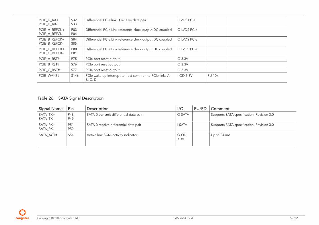
Copyright © 2017 congatec AG SA50m14.indd 59/72
PCIE_D_RX+PCIE_D_RX-
S32S33
Differential PCIe link D receive data pair I LVDS PCIe
PCIE_A_REFCK+PCIE_A_REFCK-
P83P84
Differential PCIe Link reference clock output DC coupled O LVDS PCIe
PCIE_B_REFCK+PCIE_B_REFCK-
S84S85
Differential PCIe Link reference clock output DC coupled O LVDS PCIe
PCIE_C_REFCK+PCIE_C_REFCK-
P80P81
Differential PCIe Link reference clock output DC coupled O LVDS PCIe
PCIE_A_RST# P75 PCIe port reset output O 3.3V
PCIE_B_RST# S76 PCIe port reset output O 3.3V
PCIE_C_RST# S77 PCIe port reset output O 3.3V
PCIE_WAKE# S146 PCIe wake up interrupt to host common to PCIe links A, B, C, D
I OD 3.3V PU 10k
Table 26 SATA Signal Description
Signal Name Pin Description I/O PU/PD CommentSATA_TX+ SATA_TX-
P48P49
SATA 0 transmit differential data pair O SATA Supports SATA specification, Revision 3.0
SATA_RX+ SATA_RX-
P51P52
SATA 0 receive differential data pair I SATA Supports SATA specification, Revision 3.0
SATA_ACT# S54 Active low SATA activity indicator O OD 3.3V
Up to 24 mA
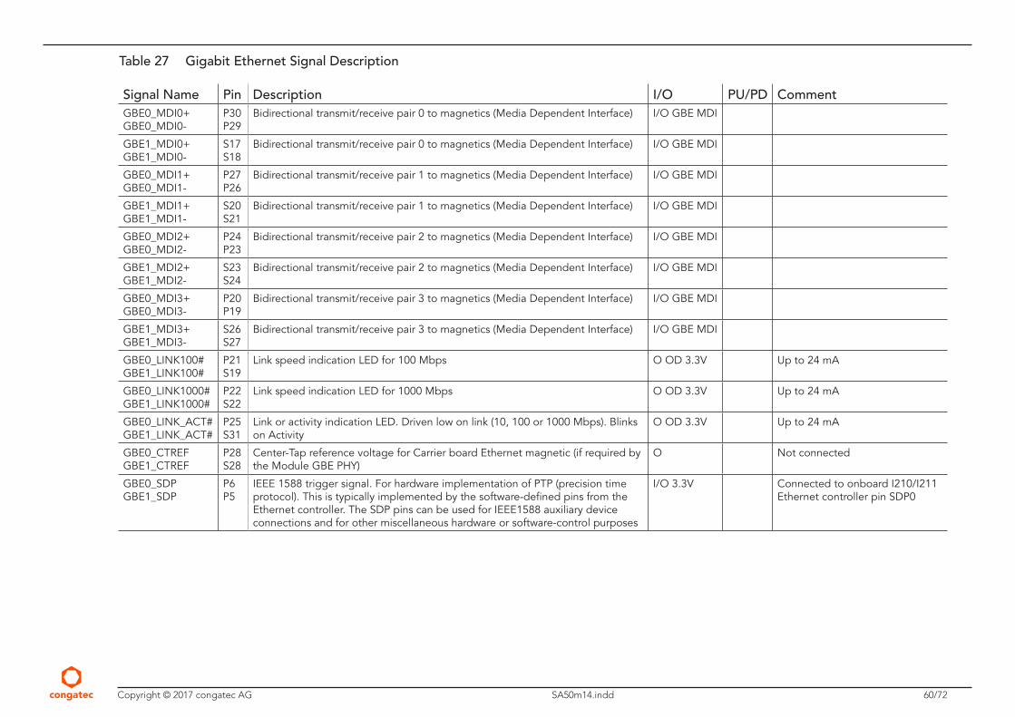
Copyright © 2017 congatec AG SA50m14.indd 60/72
Table 27 Gigabit Ethernet Signal Description
Signal Name Pin Description I/O PU/PD CommentGBE0_MDI0+GBE0_MDI0-
P30P29
Bidirectional transmit/receive pair 0 to magnetics (Media Dependent Interface) I/O GBE MDI
GBE1_MDI0+GBE1_MDI0-
S17S18
Bidirectional transmit/receive pair 0 to magnetics (Media Dependent Interface) I/O GBE MDI
GBE0_MDI1+GBE0_MDI1-
P27P26
Bidirectional transmit/receive pair 1 to magnetics (Media Dependent Interface) I/O GBE MDI
GBE1_MDI1+GBE1_MDI1-
S20S21
Bidirectional transmit/receive pair 1 to magnetics (Media Dependent Interface) I/O GBE MDI
GBE0_MDI2+GBE0_MDI2-
P24P23
Bidirectional transmit/receive pair 2 to magnetics (Media Dependent Interface) I/O GBE MDI
GBE1_MDI2+GBE1_MDI2-
S23S24
Bidirectional transmit/receive pair 2 to magnetics (Media Dependent Interface) I/O GBE MDI
GBE0_MDI3+GBE0_MDI3-
P20P19
Bidirectional transmit/receive pair 3 to magnetics (Media Dependent Interface) I/O GBE MDI
GBE1_MDI3+GBE1_MDI3-
S26S27
Bidirectional transmit/receive pair 3 to magnetics (Media Dependent Interface) I/O GBE MDI
GBE0_LINK100#GBE1_LINK100#
P21S19
Link speed indication LED for 100 Mbps O OD 3.3V Up to 24 mA
GBE0_LINK1000#GBE1_LINK1000#
P22S22
Link speed indication LED for 1000 Mbps O OD 3.3V Up to 24 mA
GBE0_LINK_ACT#GBE1_LINK_ACT#
P25S31
Link or activity indication LED. Driven low on link (10, 100 or 1000 Mbps). Blinks on Activity
O OD 3.3V Up to 24 mA
GBE0_CTREFGBE1_CTREF
P28S28
Center-Tap reference voltage for Carrier board Ethernet magnetic (if required by the Module GBE PHY)
O Not connected
GBE0_SDPGBE1_SDP
P6P5
IEEE 1588 trigger signal. For hardware implementation of PTP (precision time protocol). This is typically implemented by the software-defined pins from the Ethernet controller. The SDP pins can be used for IEEE1588 auxiliary device connections and for other miscellaneous hardware or software-control purposes
I/O 3.3V Connected to onboard I210/I211 Ethernet controller pin SDP0
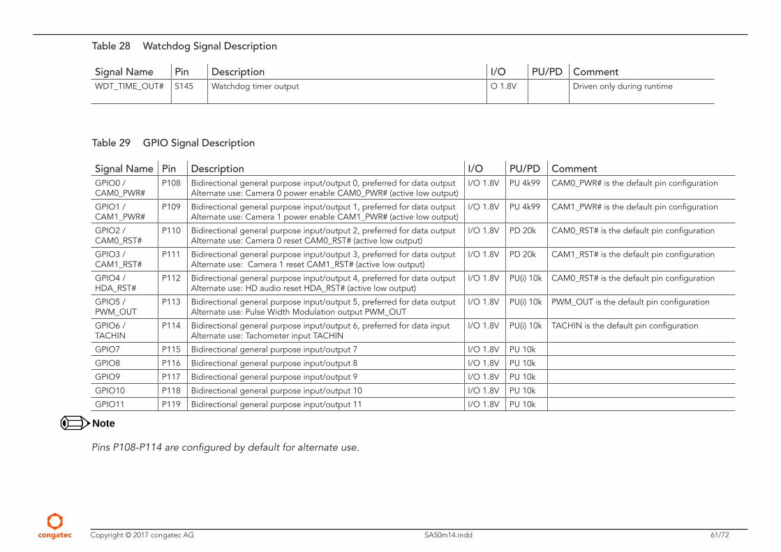
Copyright © 2017 congatec AG SA50m14.indd 61/72
Table 28 Watchdog Signal Description
Signal Name Pin Description I/O PU/PD CommentWDT_TIME_OUT# S145 Watchdog timer output O 1.8V Driven only during runtime
Table 29 GPIO Signal Description
Signal Name Pin Description I/O PU/PD CommentGPIO0 / CAM0_PWR#
P108 Bidirectional general purpose input/output 0, preferred for data outputAlternate use: Camera 0 power enable CAM0_PWR# (active low output)
I/O 1.8V PU 4k99 CAM0_PWR# is the default pin configuration
GPIO1 / CAM1_PWR#
P109 Bidirectional general purpose input/output 1, preferred for data outputAlternate use: Camera 1 power enable CAM1_PWR# (active low output)
I/O 1.8V PU 4k99 CAM1_PWR# is the default pin configuration
GPIO2 / CAM0_RST#
P110 Bidirectional general purpose input/output 2, preferred for data outputAlternate use: Camera 0 reset CAM0_RST# (active low output)
I/O 1.8V PD 20k CAM0_RST# is the default pin configuration
GPIO3 / CAM1_RST#
P111 Bidirectional general purpose input/output 3, preferred for data outputAlternate use: Camera 1 reset CAM1_RST# (active low output)
I/O 1.8V PD 20k CAM1_RST# is the default pin configuration
GPIO4 / HDA_RST#
P112 Bidirectional general purpose input/output 4, preferred for data outputAlternate use: HD audio reset HDA_RST# (active low output)
I/O 1.8V PU(i) 10k CAM0_RST# is the default pin configuration
GPIO5 / PWM_OUT
P113 Bidirectional general purpose input/output 5, preferred for data outputAlternate use: Pulse Width Modulation output PWM_OUT
I/O 1.8V PU(i) 10k PWM_OUT is the default pin configuration
GPIO6 / TACHIN
P114 Bidirectional general purpose input/output 6, preferred for data inputAlternate use: Tachometer input TACHIN
I/O 1.8V PU(i) 10k TACHIN is the default pin configuration
GPIO7 P115 Bidirectional general purpose input/output 7 I/O 1.8V PU 10k
GPIO8 P116 Bidirectional general purpose input/output 8 I/O 1.8V PU 10k
GPIO9 P117 Bidirectional general purpose input/output 9 I/O 1.8V PU 10k
GPIO10 P118 Bidirectional general purpose input/output 10 I/O 1.8V PU 10k
GPIO11 P119 Bidirectional general purpose input/output 11 I/O 1.8V PU 10k
Note
Pins P108-P114 are configured by default for alternate use.
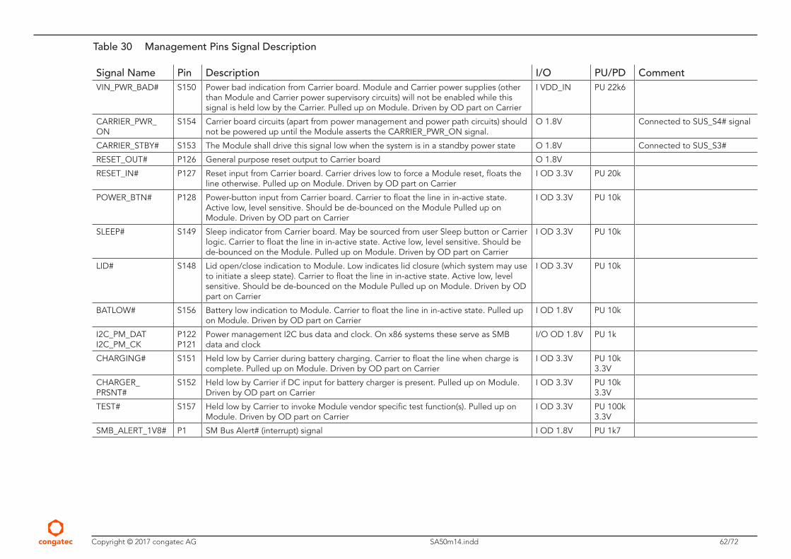
Copyright © 2017 congatec AG SA50m14.indd 62/72
Table 30 Management Pins Signal Description
Signal Name Pin Description I/O PU/PD CommentVIN_PWR_BAD# S150 Power bad indication from Carrier board. Module and Carrier power supplies (other
than Module and Carrier power supervisory circuits) will not be enabled while this signal is held low by the Carrier. Pulled up on Module. Driven by OD part on Carrier
I VDD_IN PU 22k6
CARRIER_PWR_ON
S154 Carrier board circuits (apart from power management and power path circuits) should not be powered up until the Module asserts the CARRIER_PWR_ON signal.
O 1.8V Connected to SUS_S4# signal
CARRIER_STBY# S153 The Module shall drive this signal low when the system is in a standby power state O 1.8V Connected to SUS_S3#
RESET_OUT# P126 General purpose reset output to Carrier board O 1.8V
RESET_IN# P127 Reset input from Carrier board. Carrier drives low to force a Module reset, floats the line otherwise. Pulled up on Module. Driven by OD part on Carrier
I OD 3.3V PU 20k
POWER_BTN# P128 Power-button input from Carrier board. Carrier to float the line in in-active state. Active low, level sensitive. Should be de-bounced on the Module Pulled up on Module. Driven by OD part on Carrier
I OD 3.3V PU 10k
SLEEP# S149 Sleep indicator from Carrier board. May be sourced from user Sleep button or Carrier logic. Carrier to float the line in in-active state. Active low, level sensitive. Should be de-bounced on the Module. Pulled up on Module. Driven by OD part on Carrier
I OD 3.3V PU 10k
LID# S148 Lid open/close indication to Module. Low indicates lid closure (which system may use to initiate a sleep state). Carrier to float the line in in-active state. Active low, level sensitive. Should be de-bounced on the Module Pulled up on Module. Driven by OD part on Carrier
I OD 3.3V PU 10k
BATLOW# S156 Battery low indication to Module. Carrier to float the line in in-active state. Pulled up on Module. Driven by OD part on Carrier
I OD 1.8V PU 10k
I2C_PM_DATI2C_PM_CK
P122P121
Power management I2C bus data and clock. On x86 systems these serve as SMB data and clock
I/O OD 1.8V PU 1k
CHARGING# S151 Held low by Carrier during battery charging. Carrier to float the line when charge is complete. Pulled up on Module. Driven by OD part on Carrier
I OD 3.3V PU 10k 3.3V
CHARGER_PRSNT#
S152 Held low by Carrier if DC input for battery charger is present. Pulled up on Module. Driven by OD part on Carrier
I OD 3.3V PU 10k 3.3V
TEST# S157 Held low by Carrier to invoke Module vendor specific test function(s). Pulled up on Module. Driven by OD part on Carrier
I OD 3.3V PU 100k 3.3V
SMB_ALERT_1V8# P1 SM Bus Alert# (interrupt) signal I OD 1.8V PU 1k7
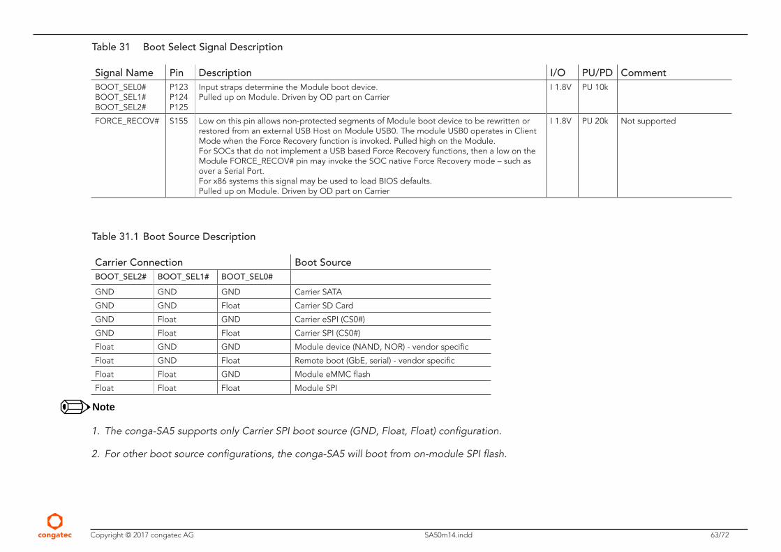
Copyright © 2017 congatec AG SA50m14.indd 63/72
Table 31 Boot Select Signal Description
Signal Name Pin Description I/O PU/PD CommentBOOT_SEL0#BOOT_SEL1#BOOT_SEL2#
P123P124P125
Input straps determine the Module boot device.Pulled up on Module. Driven by OD part on Carrier
I 1.8V PU 10k
FORCE_RECOV# S155 Low on this pin allows non-protected segments of Module boot device to be rewritten or restored from an external USB Host on Module USB0. The module USB0 operates in Client Mode when the Force Recovery function is invoked. Pulled high on the Module.For SOCs that do not implement a USB based Force Recovery functions, then a low on the Module FORCE_RECOV# pin may invoke the SOC native Force Recovery mode – such as over a Serial Port.For x86 systems this signal may be used to load BIOS defaults.Pulled up on Module. Driven by OD part on Carrier
I 1.8V PU 20k Not supported
Table 31.1 Boot Source Description
Carrier Connection Boot SourceBOOT_SEL2# BOOT_SEL1# BOOT_SEL0#
GND GND GND Carrier SATA
GND GND Float Carrier SD Card
GND Float GND Carrier eSPI (CS0#)
GND Float Float Carrier SPI (CS0#)
Float GND GND Module device (NAND, NOR) - vendor specific
Float GND Float Remote boot (GbE, serial) - vendor specific
Float Float GND Module eMMC flash
Float Float Float Module SPI
Note
1. The conga-SA5 supports only Carrier SPI boot source (GND, Float, Float) configuration.
2. For other boot source configurations, the conga-SA5 will boot from on-module SPI flash.
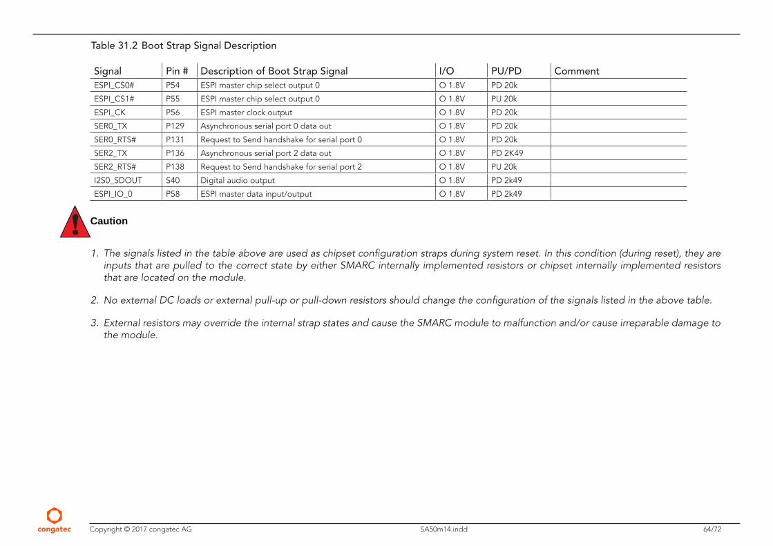
Copyright © 2017 congatec AG SA50m14.indd 64/72
Table 31.2 Boot Strap Signal Description
Signal Pin # Description of Boot Strap Signal I/O PU/PD CommentESPI_CS0# P54 ESPI master chip select output 0 O 1.8V PD 20k
ESPI_CS1# P55 ESPI master chip select output 0 O 1.8V PU 20k
ESPI_CK P56 ESPI master clock output O 1.8V PD 20k
SER0_TX P129 Asynchronous serial port 0 data out O 1.8V PD 20k
SER0_RTS# P131 Request to Send handshake for serial port 0 O 1.8V PD 20k
SER2_TX P136 Asynchronous serial port 2 data out O 1.8V PD 2K49
SER2_RTS# P138 Request to Send handshake for serial port 2 O 1.8V PU 20k
I2S0_SDOUT S40 Digital audio output O 1.8V PD 2k49
ESPI_IO_0 P58 ESPI master data input/output O 1.8V PD 2k49
Caution
1. The signals listed in the table above are used as chipset configuration straps during system reset. In this condition (during reset), they are inputs that are pulled to the correct state by either SMARC internally implemented resistors or chipset internally implemented resistors that are located on the module.
2. No external DC loads or external pull-up or pull-down resistors should change the configuration of the signals listed in the above table.
3. External resistors may override the internal strap states and cause the SMARC module to malfunction and/or cause irreparable damage to the module.
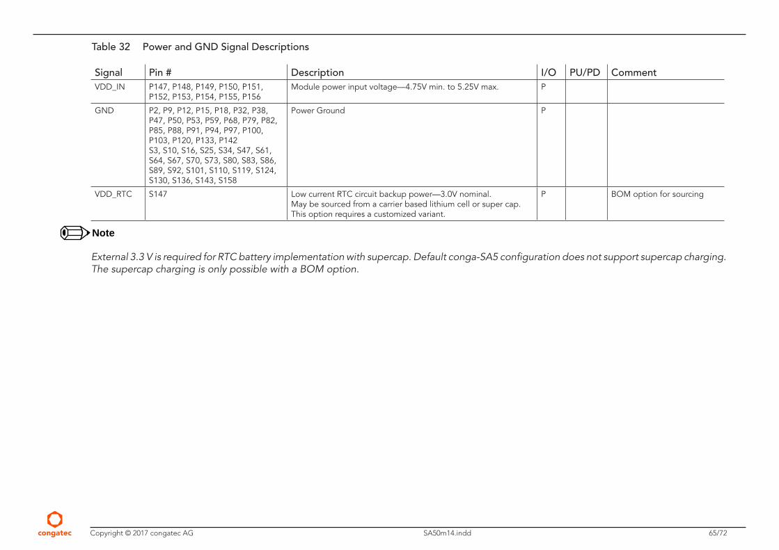
Copyright © 2017 congatec AG SA50m14.indd 65/72
Table 32 Power and GND Signal Descriptions
Signal Pin # Description I/O PU/PD CommentVDD_IN P147, P148, P149, P150, P151,
P152, P153, P154, P155, P156Module power input voltage—4.75V min. to 5.25V max. P
GND P2, P9, P12, P15, P18, P32, P38, P47, P50, P53, P59, P68, P79, P82, P85, P88, P91, P94, P97, P100, P103, P120, P133, P142S3, S10, S16, S25, S34, S47, S61, S64, S67, S70, S73, S80, S83, S86, S89, S92, S101, S110, S119, S124, S130, S136, S143, S158
Power Ground P
VDD_RTC S147 Low current RTC circuit backup power—3.0V nominal. May be sourced from a carrier based lithium cell or super cap. This option requires a customized variant.
P BOM option for sourcing
Note
External 3.3 V is required for RTC battery implementation with supercap. Default conga-SA5 configuration does not support supercap charging. The supercap charging is only possible with a BOM option.
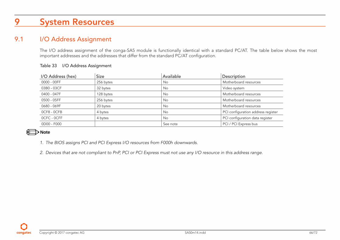
Copyright © 2017 congatec AG SA50m14.indd 66/72
9 System Resources
9.1 I/O Address Assignment
The I/O address assignment of the conga-SA5 module is functionally identical with a standard PC/AT. The table below shows the most important addresses and the addresses that differ from the standard PC/AT configuration.
Table 33 I/O Address Assignment
I/O Address (hex) Size Available Description0000 - 00FF 256 bytes No Motherboard resources
03B0 - 03CF 32 bytes No Video system
0400 - 047F 128 bytes No Motherboard resources
0500 - 05FF 256 bytes No Motherboard resources
0680 - 069F 20 bytes No Motherboard resources
0CF8 - 0CFB 4 bytes No PCI configuration address register
0CFC - 0CFF 4 bytes No PCI configuration data register
0D00 - F000 See note PCI / PCI Express bus
Note
1. The BIOS assigns PCI and PCI Express I/O resources from F000h downwards.
2. Devices that are not compliant to PnP, PCI or PCI Express must not use any I/O resource in this address range.
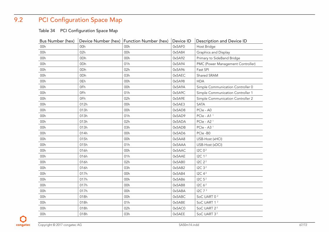
Copyright © 2017 congatec AG SA50m14.indd 67/72
9.2 PCI Configuration Space Map
Table 34 PCI Configuration Space Map
Bus Number (hex) Device Number (hex) Function Number (hex) Device ID Description and Device ID 00h 00h 00h 0x5AF0 Host Bridge
00h 02h 00h 0x5A84 Graphics and Display
00h 0Dh 00h 0x5A92 Primary to SideBand Bridge
00h 0Dh 01h 0x5A94 PMC (Power Management Controller)
00h 0Dh 02h 0x5A96 Fast SPI
00h 0Dh 03h 0x5AEC Shared SRAM
00h 0Eh 00h 0x5A98 HDA
00h 0Fh 00h 0x5A9A Simple Communication Controller 0
00h 0Fh 01h 0x5A9C Simple Communication Controller 1
00h 0Fh 02h 0x5A9E Simple Communication Controller 2
00h 012h 00h 0x5AE3 SATA
00h 013h 00h 0x5AD8 PCIe - A0
00h 013h 01h 0x5AD9 PCIe - A1 1
00h 013h 02h 0x5ADA PCIe - A2 1
00h 013h 03h 0x5ADB PCIe - A3 1
00h 014h 00h 0x5AD6 PCIe -B0
00h 015h 00h 0x5AA8 USB-Host (xHCI)
00h 015h 01h 0x5AAA USB-Host (xDCI)
00h 016h 00h 0x5AAC I2C 0 2
00h 016h 01h 0x5AAE I2C 1 2
00h 016h 02h 0x5AB0 I2C 2 2
00h 016h 03h 0x5AB2 I2C 3 2
00h 017h 00h 0x5AB4 I2C 4 2
00h 017h 00h 0x5AB6 I2C 5 2
00h 017h 00h 0x5AB8 I2C 6 2
00h 017h 00h 0x5ABA I2C 7 2
00h 018h 00h 0x5ABC SoC UART 0 2
00h 018h 01h 0x5ABE SoC UART 1 2
00h 018h 02h 0x5AC0 SoC UART 2 2
00h 018h 03h 0x5AEE SoC UART 3 2
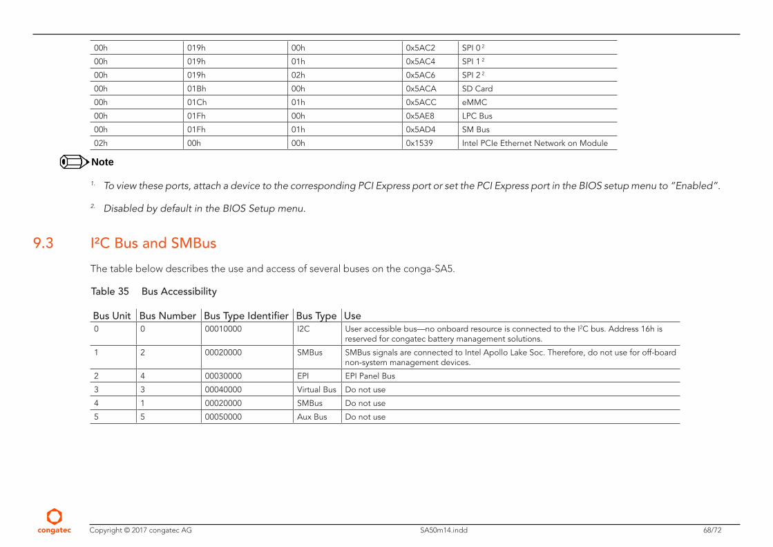
Copyright © 2017 congatec AG SA50m14.indd 68/72
00h 019h 00h 0x5AC2 SPI 0 2
00h 019h 01h 0x5AC4 SPI 1 2
00h 019h 02h 0x5AC6 SPI 2 2
00h 01Bh 00h 0x5ACA SD Card
00h 01Ch 01h 0x5ACC eMMC
00h 01Fh 00h 0x5AE8 LPC Bus
00h 01Fh 01h 0x5AD4 SM Bus
02h 00h 00h 0x1539 Intel PCIe Ethernet Network on Module
Note
1. To view these ports, attach a device to the corresponding PCI Express port or set the PCI Express port in the BIOS setup menu to “Enabled”.
2. Disabled by default in the BIOS Setup menu.
9.3 I²C Bus and SMBus
The table below describes the use and access of several buses on the conga-SA5.
Table 35 Bus Accessibility
Bus Unit Bus Number Bus Type Identifier Bus Type Use0 0 00010000 I2C User accessible bus—no onboard resource is connected to the I2C bus. Address 16h is
reserved for congatec battery management solutions.
1 2 00020000 SMBus SMBus signals are connected to Intel Apollo Lake Soc. Therefore, do not use for off-board non-system management devices.
2 4 00030000 EPI EPI Panel Bus
3 3 00040000 Virtual Bus Do not use
4 1 00020000 SMBus Do not use
5 5 00050000 Aux Bus Do not use
Copyright © 2017 congatec AG SA50m14.indd 69/72
9.4 congatec System Sensors
The conga-SA5 offers the following sensors and monitors:
• temperature sensors
– CPU temperature based on CPU Digital Thermal Sensor
– Board temperature sensor located on the Board Controller
• voltage sensors
– 5V standard voltage sensor
– 5V standby voltage sensor
• current sensor
• fan monitor
The sensors and monitors are accessible through CGOS interface, and also visible on the “Health Monitor”submenu in the BIOS Setup.
Copyright © 2017 congatec AG SA50m14.indd 70/72
10 BIOS Setup Description
10.1 Navigating the BIOS Setup Menu
The BIOS setup menu shows the features and options supported in the congatec BIOS. To access and navigate the BIOS setup menu, press the <DEL> or <F2> key during POST.
The right frame displays the key legend. Above the key legend is an area reserved for text messages. These text messages explain the options and the possible impacts when changing the selected option in the left frame.
10.2 BIOS Versions
The BIOS displays the BIOS project name and the revision code during POST, and on the main setup screen. The initial production BIOS for conga-SA5 is identified as SA50R1xx, where:
• R is the identifier for a BIOS ROM file,
• 1 is the so called feature number and
• xx is the major and minor revision number.
The SA50 binary size is 8 MB.
10.3 Updating the BIOS
OEMs often use BIOS updates to correct platform issues discovered after the board has been shipped or when new features are added to the BIOS. The conga-SA5 uses a congatec/AMI AptioEFI firmware, which is stored in an onboard flash ROM chip and can be updated using the congatec System Utility. The utility has four versions—DOS based command line, Win32 command line, Win32 GUI, and Linux version.
For more information about “Updating the BIOS” refer to the user’s guide for the congatec System Utility “CGUTLm1x.pdf” on the congatec website at www.congatec.com.
Copyright © 2017 congatec AG SA50m14.indd 71/72
10.4 Supported Flash Devices
The conga-SA5 supports the following flash devices:
• Winbond W25Q64FWSSIQ (8 MB)
• Macronix MX25U6473FM2I-10G (8 MB)
• GigaDevice GD25LB64CSIG (8 MB)
The flash devices listed above can be used on the carrier board to support external BIOS. For more information about external BIOS support, refer to the Application Note AN7_External_BIOS_Update.pdf on the congatec website at http://www.congatec.com.
Copyright © 2017 congatec AG SA50m14.indd 72/72
11 Industry SpecificationsTable 36 References
Specification LinkSMARC® Specification http://www.SMARC-standard.org/
SMARC® Design Guide http://www.SMARC-standard.org/
Low Pin Count Interface Specification, Revision 1.0 (LPC) http://developer.intel.com/design/chipsets/industry/lpc.htm
Universal Serial Bus (USB) Specification, Revision 2.0 http://www.usb.org/home
Serial ATA Specification, Revision 1.0a http://www.serialata.org
PCI Express Base Specification, Revision 2.0 http://www.pcisig.com/specifications