connectcore xp 270 hardware referenceftp1.digi.com/support/documentation/90000759_c.pdf ·...
TRANSCRIPT
Part number/version: 90000759_CRelease date: August 2007www.digi.com
ConnectCore™ XP 270 Hardware Reference

Digi International11001 Bren Road EastMinnetonka, MN 55343 U.S.A.United States: +1 877 912-3444Other locations: +1 952 912-3444
www.digi.com/support/www.digi.com
©2005-2006 Digi International Inc.Printed in the United States of America. All rights reserved.
Digi, Digi International, the Digi logo, the Making Device Networking Easy logo, NetSilicon, a Digi International Company, NET+, NET+OS and NET+Works are trademarks or registered trademarks of Digi International, Inc. in the United States and other countries worldwide. All other trademarks are the property of their respective owners.
Information in this document is subject to change without notice and does not represent a committment on the part of Digi International.
Digi provides this document “as is,” without warranty of any kind, either expressed or implied, including, but not limited to, the implied warranties of, fitness or merchantability for a particular purpose. Digi may make improvements and/or changes in this manual or in the product(s) and/or the program(s) described in this manual at any time.
This product could include technical inaccuracies or typographical errors. Changes are made periodically to the information herein; these changes may be incorporated in new editions of the publication.
Contents
Documentation updates .............................................................. viii
C h a p t e r 1 : A b o u t t h e M o d u l e ................................................................................... 1
Intel XScale PXA270 ..................................................................... 2ConnectCore XP 270 module ........................................................... 3
Using the ConnectCore XP 270 chip select.................................... 5Reset Logic......................................................................... 6Watchdog .......................................................................... 6Clock signals ....................................................................... 7Flash memory ..................................................................... 7SDRAM memory.................................................................... 7Power Management Chip for PXA270 processor .............................. 8Ethernet Controller............................................................... 9External schematics for SMSC LAN91C111 Ethernet Controller........... 101-Wire EEPROM................................................................... 12USB................................................................................. 14UARTs.............................................................................. 20SSP Serial Ports................................................................... 21I²C Bus Interface ................................................................. 22PC Card and CompactFlash Interface......................................... 22MultiMedia Card / SD / SDIO Controller + Memory Stick................... 23LCD Controller.................................................................... 24AC’97 Controller ................................................................. 27Pulse Width Modulator Controller............................................. 27
Connector pinout ....................................................................... 28ConnectCore XP pinouts: Connector X1 ...................................... 28
n n n n n n n i i i
ConnectCore XP pinouts: Connector X2 ...................................... 33ConnectCore XP 270 GPIOs............................................................ 36
Bidirectional GPIOs .............................................................. 37ConnectCore XP 270 GPIO use ................................................. 37GPIO Controller Register Summary............................................ 46GPIOs used internally ........................................................... 47
ConnectCore XP 270 Memory Map.................................................... 48
C h a p t e r 2 : A b o u t t h e D e v e l o p m e n t B o a r d .................................................51
XScale .................................................................................... 52What’s on the development board?.................................................. 53
General Precautions............................................................. 54Installation............................................................................... 55
Replacing the module ........................................................... 55Setting up basic and optional connections................................... 57
Hardware block diagram .............................................................. 58LEDs and selection of Ethernet magnetics.......................................... 59Jumpers .................................................................................. 59Pin descriptions ......................................................................... 61ConnectCore XP 270 X1 pinout ....................................................... 77ConnectCore XP 270 X2 pinout ....................................................... 81
C h a p t e r 3 : C o n n e c t C o r e X P 2 7 0 C u s t o m i z a t i o n ..................................87
Adding custom hardware to the development board ............................. 88Custom development board design check list...................................... 88
A p p e n d i x A : C o n n e c t C o r e X P 2 7 0 M o d u l e S p e c i f i c a t i o n s 9 1Mechanical dimensions ................................................................ 92Environmental information............................................................ 93Power requirements.................................................................... 94Layout considerations.................................................................. 94
A p p e n d i x A : J T A G - B o o s t e r f o r I n t e l X S c a l e P X A 2 7 0 9 7Overview ................................................................................. 98System requirements................................................................... 98
iv
CD files ................................................................................... 99Connecting your PC to the target system .......................................... 99Initialization file JTAG270.INI .......................................................100Supported Flash devices ..............................................................100JTAG270 Parameter Description ....................................................101Program a Flash Device ...............................................................103
Use: JTAG270 /P filename [optionlist] ......................................103Options ...........................................................................103
Example with Intel PXA270...........................................................106Support for Windows NT, Windows 2000 and Windows XP ......................107
Installation on a clean system ................................................108Installation with an already installed version 5.x/6.x of Kithara .......108
v

Using This Guide Using This Guide
Review this section for basic information about the guide you are using, as well as general support and contact information.
About this guide
This guide provides information about the Digi ConnectCore XP 270, a fully integrated system-on-chip solution on a 67.6 x 36.7mm card.
The ConnectCore XP 270 module is built on the Intel XScale processor PXA270, flash and SDRAM memory, and the SMSC LAN91C111 Ethernet controller.
What’s in this guide
This table shows where you can find specific information in this guide.
To read about See
ConnectCore XP 270 module Chapter 1, “About the Module”
ConnectCore XP development board Chapter 2, “About the Development Board”
Customizing the ConnectCore XP 270 Chapter 3, “ConnectCore XP 270 Customization”
Module specifications Appendix A, “ConnectCore XP 270 Module Specifications
v i i
D o c u m e n t a t i o n u p d a t e s
Conventions used in this guide
This table describes the typographic conventions used in this guide:
Related documentation
Intel® PXA27x Processor Family
Developer’s Manual
October 2004
Order Number: 280000-002
Documentation updates
Digi occasionally provides documentation updates on the Web site (www.digi.com/support).
Be aware that if you see differences between the documentation you received in your package and the documentation on the Web site, the Web site content is the latest version.
Using the JTAG-Booster Appendix B, “JTAG -Booster for Intel XScale PXA270”
To read about See
This convention Is used for
italic type Emphasis, new terms, variables, and document titles.
monospaced type Filenames, pathnames, and code examples.
v i i i C o n n e c t C o r e X P 2 7 0 H a r d w a r e R e f e r e n c e , R e v . C 0 8 / 2 0 0 7

Customer support
To get help with a question or technical problem with this product, or to make comments and recommendations about our products or documentation, use the contact information listed in this table:
For Contact information
Technical support United States: +1 877 912-3444Other locations: +1 952 912-3444www.digi.com/supportwww.digi.com
w w w . d i g i . c o m i x

About the ModuleC H A P T E R 1
The ConnectCore XP 270 module is a fully integrated system-on-chip solution on a 67.6 x 36.7mm card — a system built on Intel XScale processor PXA270, flash and SDRAM memory, and the SMSC LAN91C111 Ethernet controller.
1
I n t e l X S c a l e P X A 2 7 0
Intel XScale PXA270
Features
Intel XScale Technology highly scalable core from 104 MHz up to 520 MHz
Little Endian operation
Embedded Packaging: 23 x 23 mm with 1.0 mm ball pitch
Enhanced LCD Controller
Large Peripheral Set:
– USB Host / Client
– USB OTG
– PCMCIA / Compact Flash
– IrDA
– I²C
– AC97 Controller
– Full Function UART
– Bluetooth UART
– LCD controller
– SSP and NSSP Serial ports
2 C o n n e c t C o r e X P 2 7 0 H a r d w a r e R e f e r e n c e , R e v . C 0 8 / 2 0 0 7
A b o u t t h e M o d u l e
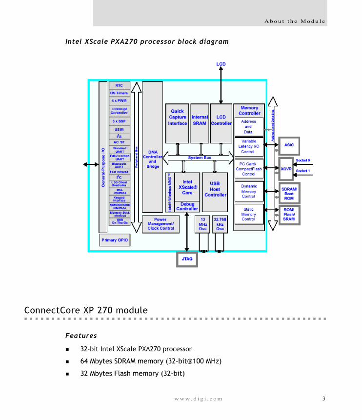
Intel XScale PXA270 processor block diagram
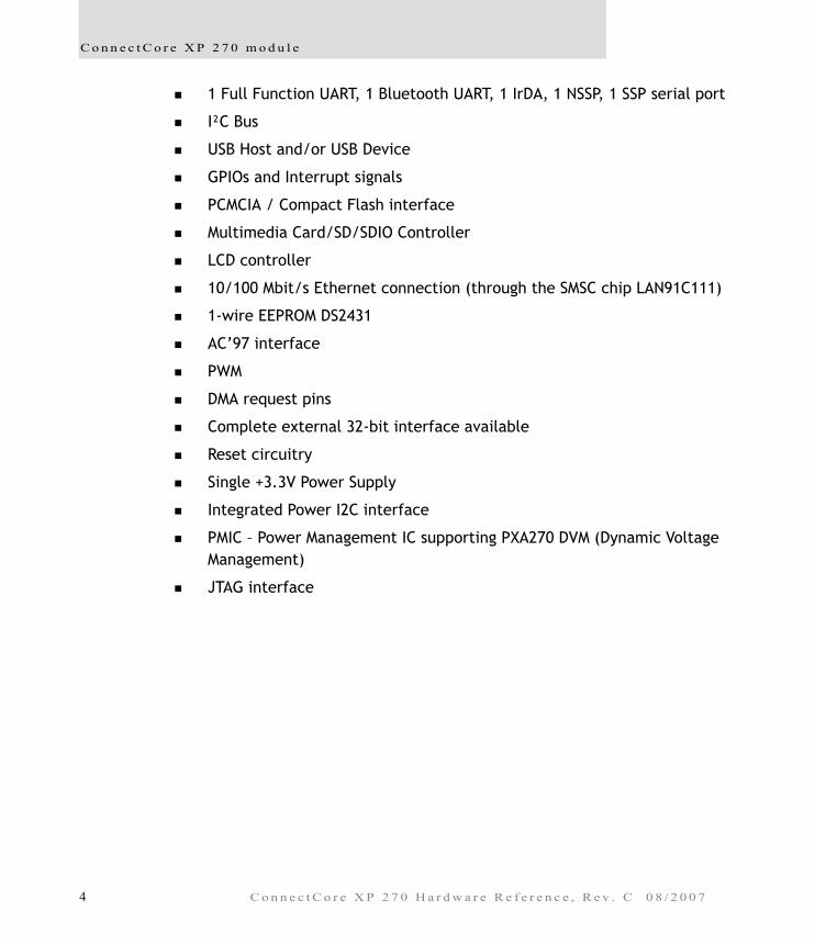
ConnectCore XP 270 module
Features
32-bit Intel XScale PXA270 processor
64 Mbytes SDRAM memory (32-bit@100 MHz)
32 Mbytes Flash memory (32-bit)
w w w . d i g i . c o m 3
C o n n e c t C o r e X P 2 7 0 m o d u l e
1 Full Function UART, 1 Bluetooth UART, 1 IrDA, 1 NSSP, 1 SSP serial port
I²C Bus
USB Host and/or USB Device
GPIOs and Interrupt signals
PCMCIA / Compact Flash interface
Multimedia Card/SD/SDIO Controller
LCD controller
10/100 Mbit/s Ethernet connection (through the SMSC chip LAN91C111)
1-wire EEPROM DS2431
AC’97 interface
PWM
DMA request pins
Complete external 32-bit interface available
Reset circuitry
Single +3.3V Power Supply
Integrated Power I2C interface
PMIC – Power Management IC supporting PXA270 DVM (Dynamic Voltage Management)
JTAG interface
4 C o n n e c t C o r e X P 2 7 0 H a r d w a r e R e f e r e n c e , R e v . C 0 8 / 2 0 0 7
A b o u t t h e M o d u l e
ConnectCore XP 270 module
Using the ConnectCore XP 270 chip select
PXA27x SDRAM FLASH ETHERNET
SILICONNUMBER
COREVOLTAGE
RESETCONTROLLER
X1 X2
+3.3V
Data, Address, Ethernet, AC97, LCD, UART, Bluetooth, PCMCIA,USB, JTAG, NSSP, SSP, IrDA, Multimedia Card, GPIOs
Chip Select Use
CS0# Flash memory
CS1# Ethernet Controller – SMSC LAN91C111
CS2# Free for external use
CS3# Free for external use
CS4# Free for external use
CS5# Free for external use
w w w . d i g i . c o m 5
C o n n e c t C o r e X P 2 7 0 m o d u l e
Reset Logic
The Connect Core XP 270 module has two reset signals:
RESET_IN#
RESET_OUT#
Both signals are low-active. If RESET_IN# is activated outside the module (through reset controller or reset button), the signal is first debounced by the on-board reset circuitry (MAXIM MAX6390XS29D4 chip) and a reset signal is transmitted to the PXA270 processor. The reset input of the PXA270 can also be activated by a power-on sequence.
Once the processor receives the reset input signal, it resets its internal peripherals and a processor specific output reset signal — RESET_OUT# — becomes active. This signal is available on ConnectCore XP 270 connectors.
On-board flash memories receive the reset signal through the RESET_IN# pin and the Ethernet controller receives the reset signal through the RESET_OUT# signal.
Intel PXA270 power-on sequence timing is fully respected on the ConnectCore XP 270 module — no special care has to be taken outside the module. For more information about power on timing, see “Intel PXA270 Processor Electrical, Mechanical and Thermal Specification – Order Number 280002-004 p.64.”
Watchdog
The Intel XScale PXA270 processor comes with a watchdog unit. The processor’s OSCR0 register can be programmed to generate a watchdog-reset signal. When the OWER[WME] field is set, the OSCR0 register is compared to the OSMR3 register every rising edge of the internal-made 3.25MHz clock.
If a match is detected, the OS timer asserts the internal WDOG_RST pin, which asserts the RESET_OUT# pin. A reset is applied to the PXA270 processor and most internal states are cleared.
Once enabled, the watchdog function can be disabled only by one of the reset functions (hardware reset, watchdog reset, or GPIO reset). Writing a zero to the Watchdog Match Enable bit after it has been set has no effect.
For more information about the watchdog unit, see the “Intel PXA27x Processor Family Developer’s Manual – Order Number: 280000-002”.
6 C o n n e c t C o r e X P 2 7 0 H a r d w a r e R e f e r e n c e , R e v . C 0 8 / 2 0 0 7
A b o u t t h e M o d u l e
Clock signals
The processor needs two clock signals:
The 13-MHz processor oscillator provides the primary clock source for the PXA270 processor. The on-chip PLL frequency multipliers and several peripheral modules use the processor oscillator as a reference. If the application has not enabled the 32.768-kHz timekeeping oscillator, the processor oscillator also drives the real-time clock (RTC) and power manager.
The 32.768-kHz timekeeping oscillator is a low-power, low-frequency oscillator that clocks the real-time clock (RTC) and power manager.
Both clock sources are used and implemented on the ConnectCore XP 270 module.
Flash memory
The ConnectCore XP 270 module support two Intel StrataFlash Flash Memory chips. Each chip is 16-bit wide, making a whole 32-bit Flash Memory area. All accesses to the flash memory are made with 32-bit words.
The Flash Memory chips are controlled by CS0#, so the module can support a maximum of 64MB of memory. Flash Memory chips have an initial access speed of 120ns and a block sector size of 64-Kword (= 128-Kbyte).
The Flash Memories reset signal is connected to the RESET_IN# input signal. With this choice, Flash Memories aren’t reset for software reset events such as sleep mode, watchdog reset, and GPIO reset.
SDRAM memory
Intel PXA270 processor supports a SDRAM interface at a maximum frequency of 104 MHz. On the ConnectCore XP 270 module, two SDRAM memory chips have been connected to the processor SDRAM partition 0 (controlled by SDCS0# signal).
There are two possible considerations regarding the size of SDRAM partition on a PXA270-based product:
Use a normal 256-Mbyte memory map; in this case, the SDRAM partition is 64-Mbyte wide.
w w w . d i g i . c o m 7
C o n n e c t C o r e X P 2 7 0 m o d u l e
Use a large 1-Gbyte memory map; in this case, the SDRAM partition is 256-Mbyte wide. This memory map allows the possibility of connecting to bigger SDRAM chips.
Note: As far as SDRAM signals available on ConnectCore XP 270 module connectors, the signals are available as references only. The module has not been adapted to support SDRAM memory outside the module, nor “length-adapted” to support PXA270 SDRAM timing.
Power Management Chip for PXA270 processor
The ConnectCore XP 270 module comes with an integrated chip that manages Intel XScale PXA270 voltages and can implement some minor power management functions. The chip is a versatile power management IC designed especially for the XScale type of processors. The chip contain three regulators, which share a common enable pin. When disabled using the enable pin, the chip enters a low-power state.
To assure stability and minimize overshoot at start-up and during DVM transitions, Power Management IC implements a controlled rise time of each regulator output.
This is a short list of available features implemented by the PMIC (Power Management Integrated Circuit):
Three voltage regulators (1 Buck for core voltage, 2 LDOs for SRAM, and PLL voltage)
Full-integrated synchronous buck regulator with DVM (Dynamic Voltage Management) — 800mA DC output current
I²C interface module for DVM from 0.58V to 1.6V
Battery fault signal
Input supply voltage range: 2.76V – 5.5V
4x4 mm QFN package
Note: The power management chip doesn’t control all the XScale PXA270 voltages. The other voltages (VCC_LCD, VCC_MEM, VCC_IO, VCC_BB, VCC_USB) are controlled directly by a MOS switch from main +3.3 Vdc power supply.
8 C o n n e c t C o r e X P 2 7 0 H a r d w a r e R e f e r e n c e , R e v . C 0 8 / 2 0 0 7
A b o u t t h e M o d u l e
Ethernet Controller
The ConnectCore XP 270 module provides an Ethernet connection (Link + PHY Layer) directly on the module board. This connection is made with the LAN91C111 chip from SMSC.
These are features of the chip:
10/100 non-PCI Ethernet Single Chip Ethernet Controller (MAC + PHY)
Fully supports Full Duplex Switched Ethernet
Supports burst data transfer
8 Kbytes internal memory for receive and transmit FIFO buffers
Supports 16 and 32-bit CPU accesses
Internal 32 bit wide data path (into packet buffer memory)
3.3V operation with 5V tolerant I/O buffers
Single 25 MHz reference clock for both PHY and MAC
128-pin TQFP package, 1.0 mm height
Industrial temperature range from -40°C to 85°C
Fully integrated IEEE 802.3/802.3u - 100BASE-TX/10BASE-T physical layer
Auto negotiation: 10/100, full/half duplex
LED outputs (user selectable, up to 2 LED functions at one time): link, activity, full duplex,10/100, transmit, and receive
The Intel PXA270 processor CS1# signal enables accesses to the Ethernet Controller chip. Although the chip can be accessed in 8, 16, and 32-bit accesses, ConnectCore XP 270 has been designed to support only 16-bit and 32-bit accesses.
The memory area reserved for the ConnectCore XP 270 Ethernet Controller is 0x0400 0300 to 0x0400 030F. Accesses to the chip are made with the PXA270 processor’s VLIO (Variable Latency) interface. LAN91C111 has no special external EEPROM, but receive the MAC address from the 1-wire EEPROM.
The LAN91C111 interrupt pin is connected to the PXA270 processor GPIO90 pin.
w w w . d i g i . c o m 9
C o n n e c t C o r e X P 2 7 0 m o d u l e
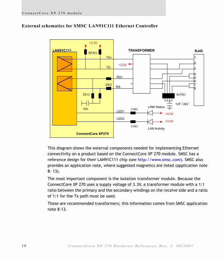
External schematics for SMSC LAN91C111 Ethernet Controller
This diagram shows the external components needed for implementing Ethernet connectivity on a product based on the ConnectCore XP 270 module. SMSC has a reference design for their LAN91C111 chip (see http://www.smsc.com). SMSC also provides an application note, where suggested magnetics are listed (application note 8- 13).
The most important component is the isolation transformer module. Because the ConnectCore XP 270 uses a supply voltage of 3.3V, a transformer module with a 1:1 ratio between the primary and the secondary windings on the receive side and a ratio of 1:1 for the Tx path must be used.
These are recommended transformers; this information comes from SMSC application note 8-13.
4x75Ω
ConnectCore XP270
LAN91C111
+3.3V
49.9Ω
10n
24 Ω
24Ω
TRANSFORMER
+3.3V
+3.3V
+3.3V
330Ω
330ΩLAN Activity
LED1
LED2
RX+
RX-
TX+
TX-
1
2
3
45678
RJ45
1nF / 2kVLINK Status
1 0 C o n n e c t C o r e X P 2 7 0 H a r d w a r e R e f e r e n c e , R e v . C 0 8 / 2 0 0 7
A b o u t t h e M o d u l e
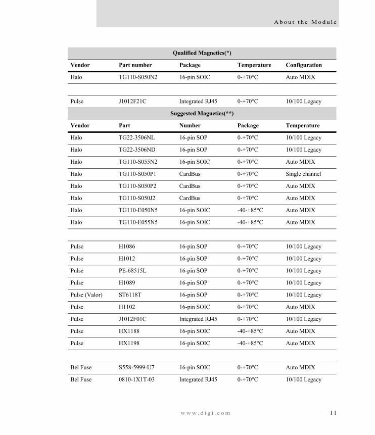
Qualified Magnetics(*)
Vendor Part number Package Temperature Configuration
Halo TG110-S050N2 16-pin SOIC 0-+70°C Auto MDIX
Pulse J1012F21C Integrated RJ45 0-+70°C 10/100 Legacy
Suggested Magnetics(**)
Vendor Part Number Package Temperature
Halo TG22-3506NL 16-pin SOP 0-+70°C 10/100 Legacy
Halo TG22-3506ND 16-pin SOP 0-+70°C 10/100 Legacy
Halo TG110-S055N2 16-pin SOIC 0-+70°C Auto MDIX
Halo TG110-S050P1 CardBus 0-+70°C Single channel
Halo TG110-S050P2 CardBus 0-+70°C Auto MDIX
Halo TG110-S050J2 CardBus 0-+70°C Auto MDIX
Halo TG110-E050N5 16-pin SOIC -40-+85°C Auto MDIX
Halo TG110-E055N5 16-pin SOIC -40-+85°C Auto MDIX
Pulse H1086 16-pin SOP 0-+70°C 10/100 Legacy
Pulse H1012 16-pin SOP 0-+70°C 10/100 Legacy
Pulse PE-68515L 16-pin SOP 0-+70°C 10/100 Legacy
Pulse H1089 16-pin SOP 0-+70°C 10/100 Legacy
Pulse (Valor) ST6118T 16-pin SOP 0-+70°C 10/100 Legacy
Pulse H1102 16-pin SOIC 0-+70°C Auto MDIX
Pulse J1012F01C Integrated RJ45 0-+70°C 10/100 Legacy
Pulse HX1188 16-pin SOIC -40-+85°C Auto MDIX
Pulse HX1198 16-pin SOIC -40-+85°C Auto MDIX
Bel Fuse S558-5999-U7 16-pin SOIC 0-+70°C Auto MDIX
Bel Fuse 0810-1X1T-03 Integrated RJ45 0-+70°C 10/100 Legacy
w w w . d i g i . c o m 1 1
C o n n e c t C o r e X P 2 7 0 m o d u l e
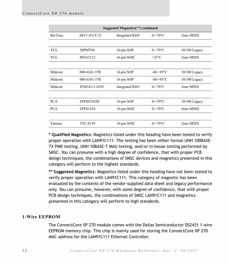
* Qualified Magnetics: Magnetics listed under this heading have been tested to verify proper operation with LAN91C111. The testing has been either formal UNH 100BASE-TX PMD testing, UNH 10BASE-T MAU testing, and/or in-house testing performed by SMSC. You can presume with a high degree of confidence, that with proper PCB design techniques, the combinations of SMSC devices and magnetics presented in this category will perform to the highest standards.
** Suggested Magnetics: Magnetics listed under this heading have not been tested to verify proper operation with LAN91C111. This category of magnetic has been evaluated by the contents of the vendor-supplied data sheet and legacy performance only. You can presume, however, with some degree of confidence, that with proper PCB design techniques, the combinations of SMSC LAN91C111 and magnetics presented in this category will perform to high standards.
1-Wire EEPROM
The ConnectCore XP 270 module comes with the Dallas Semiconductor DS2431 1-wire EEPROM memory chip. This chip is mainly used for storing the ConnectCore XP 270 MAC address for the LAN91C111 Ethernet Controller.
Suggested Magnetics(**) continued
Bel Fuse 0817-1G1T-21 Integrated RJ45 0-+70°C Auto MDIX
YCL 20PMT04 16-pin SOP 0-+70°C 10/100 Legacy
YCL PH163112 16-pin SOIC +25°C Auto MDIX
Midcom 000-6241-37R 16-pin SOP -40-+85°C 10/100 Legacy
Midcom 000-6181-37R 16-pin SOP -40-+85°C 10/100 Legacy
Midcom JFM24111-0101 Integrated RJ45 0-+70°C Auto MDIX
PCA EPF8033GM 16-pin SOP 0-+70°C 10/100 Legacy
PCA EPF8143S 16-pin SOIC 0-+70°C Auto MDIX
Tamura TTC-8139 16-pin SOIC 0-+70°C Auto MDIX
1 2 C o n n e c t C o r e X P 2 7 0 H a r d w a r e R e f e r e n c e , R e v . C 0 8 / 2 0 0 7

A b o u t t h e M o d u l e
The memory chip also provides these features:
1024-bit EEPROM memory organized as four memory pages of 256 bits each.
Memory pages that can be individually write-protected or put in EPROM-emulation mode
8-byte scratch pad
Communication over the single-conductor 1-wire bus. Communication follows standard Dallas Semiconductor 1-wire protocol.
Communication with Host with a single digital signal at 15.4kbps or 111kbps using the 1-wire protocol
Its own unalterable and unique 64-bit ROM registration number that is factory lasered into the chip
The DS2431 is a 1024-bit 1-wire EEPROM chip organized as four memory pages of 256-bit each. Data is written to an 8-byte scratch pad, verified and then copied to the EEPROM memory.
The ConnectCore XP 270 module uses GPIO87 for “bit-toggling” and implementing the 1-wire protocol to communicate with this device. For more information, see the DS2431 datasheet.
This table shows the 1-wire EEPROM memory map:
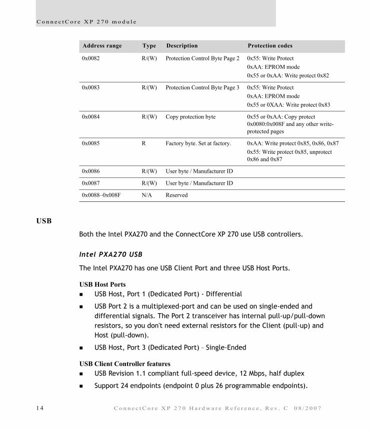
Address range Type Description Protection codes
0x000–0x001F R/(W) Data Memory Page 0Used for MAC ADDRESS
0x0020–0x003F R/(W) Data Memory Page 1
0x0040–0x005F R/(W) Data Memory Page 2
0x0060–0x007F R/(W) Data Memory Page 3
0x0080 R/(W) Protection Control Byte Page 0 0x55: Write Protect0xAA: EPROM mode0x55 or 0xAA: Write protect 0x80
0x0081 R/(W) Protection Control Byte Page 1 0x55: Write Protect0xAA: EPROM mode0x55 or 0xAA: Write protect 0x81
w w w . d i g i . c o m 1 3
C o n n e c t C o r e X P 2 7 0 m o d u l e
USB
Both the Intel PXA270 and the ConnectCore XP 270 use USB controllers.
Intel PXA270 USB
The Intel PXA270 has one USB Client Port and three USB Host Ports.
USB Host PortsUSB Host, Port 1 (Dedicated Port) - Differential
USB Port 2 is a multiplexed-port and can be used on single-ended and differential signals. The Port 2 transceiver has internal pull-up/pull-down resistors, so you don't need external resistors for the Client (pull-up) and Host (pull-down).
USB Host, Port 3 (Dedicated Port) – Single-Ended
USB Client Controller featuresUSB Revision 1.1 compliant full-speed device, 12 Mbps, half duplex
Support 24 endpoints (endpoint 0 plus 26 programmable endpoints).
0x0082 R/(W) Protection Control Byte Page 2 0x55: Write Protect0xAA: EPROM mode0x55 or 0xAA: Write protect 0x82
0x0083 R/(W) Protection Control Byte Page 3 0x55: Write Protect0xAA: EPROM mode0x55 or 0XAA: Write protect 0x83
0x0084 R/(W) Copy protection byte 0x55 or 0xAA: Copy protect 0x0080:0x008F and any other write-protected pages
0x0085 R Factory byte. Set at factory. 0xAA: Write protect 0x85, 0x86, 0x870x55: Write protect 0x85, unprotect 0x86 and 0x87
0x0086 R/(W) User byte / Manufacturer ID
0x0087 R/(W) User byte / Manufacturer ID
0x0088–0x008F N/A Reserved
Address range Type Description Protection codes
1 4 C o n n e c t C o r e X P 2 7 0 H a r d w a r e R e f e r e n c e , R e v . C 0 8 / 2 0 0 7
A b o u t t h e M o d u l e
USB Host Controller featuresUSB Revision 1.1 compatible
Supports both low-speed and full-speed USB Devices
Open Host Controller Interface (OHCI) Rev 1.0a compatible
Root hub supports two downstream ports
USB On-The-Go operationThe processor USB Device and Host controllers provide A- and B-device On-The-Go (OTG) operation as specified in the “On-The-Go Supplement to the USB 2.0 Specification”.
The on-chip OTG transceivers provide on-chip pull-up and pull-down resistors as specified in the “Pull-up / Pull-down Engineering Change Notice to the USB 2.0 Specification”.
OTG operation requires user intervention, but interrupts are provided to notify the user of OTG activities including Vbus changes, session detection, and OTG ID changes. The user must use these interrupts along with the OTG control and status registers to operate as an OTG device.
The USB OTG support includes:
Decoding SET_FEATURE commands with OTG specific selector values
Control for on-chip OTG transceiver with multiplexing between UDC and USB Host Controller Port 2
Control for on-chip OTG transceiver with multiplexing between UDC and USB Device Controller
Control, status, and interrupt registers for interfacing to off-chip OTG transceivers
Control, status, and interrupt registers for interfacing to off-chip charge pump devices
OTG ID support
ConnectCore XP 270 USB
The ConnectCore XP 270 module only has two USB signals (although the Intel XScale PXA270 processor simultaneously supports USB Host and Device).
w w w . d i g i . c o m 1 5
C o n n e c t C o r e X P 2 7 0 m o d u l e
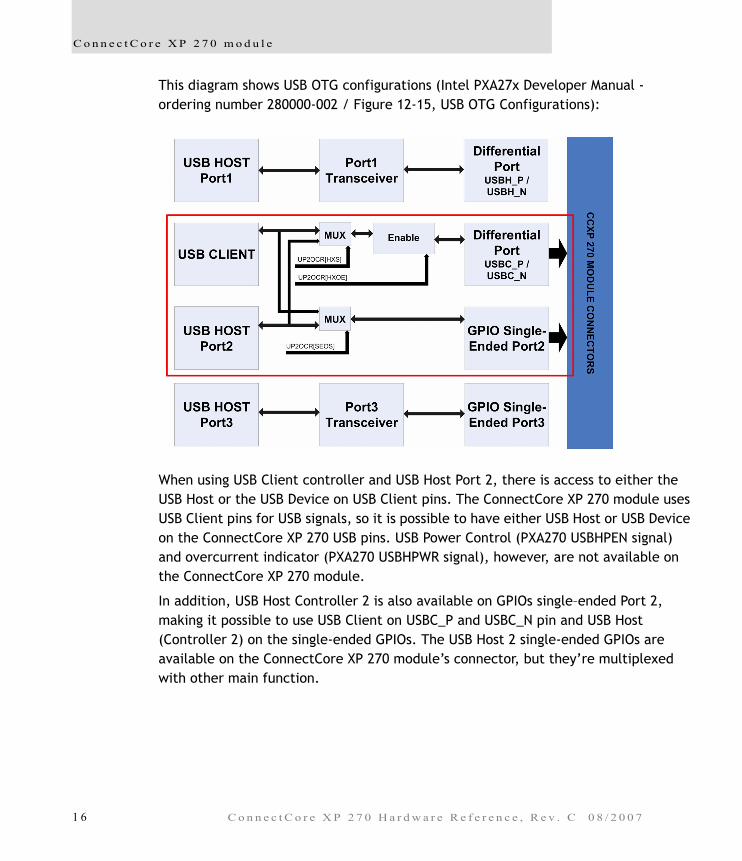
This diagram shows USB OTG configurations (Intel PXA27x Developer Manual - ordering number 280000-002 / Figure 12-15, USB OTG Configurations):
When using USB Client controller and USB Host Port 2, there is access to either the USB Host or the USB Device on USB Client pins. The ConnectCore XP 270 module uses USB Client pins for USB signals, so it is possible to have either USB Host or USB Device on the ConnectCore XP 270 USB pins. USB Power Control (PXA270 USBHPEN signal) and overcurrent indicator (PXA270 USBHPWR signal), however, are not available on the ConnectCore XP 270 module.
In addition, USB Host Controller 2 is also available on GPIOs single–ended Port 2, making it possible to use USB Client on USBC_P and USBC_N pin and USB Host (Controller 2) on the single-ended GPIOs. The USB Host 2 single-ended GPIOs are available on the ConnectCore XP 270 module’s connector, but they’re multiplexed with other main function.
1 6 C o n n e c t C o r e X P 2 7 0 H a r d w a r e R e f e r e n c e , R e v . C 0 8 / 2 0 0 7
A b o u t t h e M o d u l e
The next table shows the multiplexing mechanism:
If both USB Host and Device must be implemented on the ConnectCore XP 270 module, the following signals need to be sacrificed: FF_CTS# / GPIO35, GPIO34, FF_RI# / GPIO38, FF_DCD# / GPIO36, FF_DTR# / GPIO40, FF_TXD / GPIO39, FF_RTS# / GPIO41 and FF_DSR# / GPIO37.
With USB single-ended GPIOs you can interface an external OTG transceiver, an external charge pump device, and an external USB transceiver. The drawings on the next pages show details.
USB Host Controller single-ended signal ConnectCore XP 270 signal, with which it’s multiplexed
USB_P2_1 FF_CTS# / GPIO35
USB_P2_2 GPIO34
USB_P2_3 FF_RI# / GPIO38
USB_P2_4 FF_DCD# / GPIO36
USB_P2_5 FF_DTR# / GPIO40
USB_P2_6 FF_TXD / GPIO39
USB_P2_7 FF_RTS# / GPIO41
USB_P2_8 FF_DSR# / GPIO37
w w w . d i g i . c o m 1 7

C o n n e c t C o r e X P 2 7 0 m o d u l e
OTG Transceiver (see Intel PXA27x Developer Manual – Ordering Number 280000-002 /Figure 12-17)
1 8 C o n n e c t C o r e X P 2 7 0 H a r d w a r e R e f e r e n c e , R e v . C 0 8 / 2 0 0 7
A b o u t t h e M o d u l e
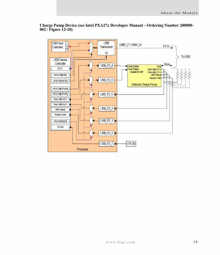
Charge Pump Device (see Intel PXA27x Developer Manual – Ordering Number 280000-002 / Figure 12-18)
w w w . d i g i . c o m 1 9
C o n n e c t C o r e X P 2 7 0 m o d u l e
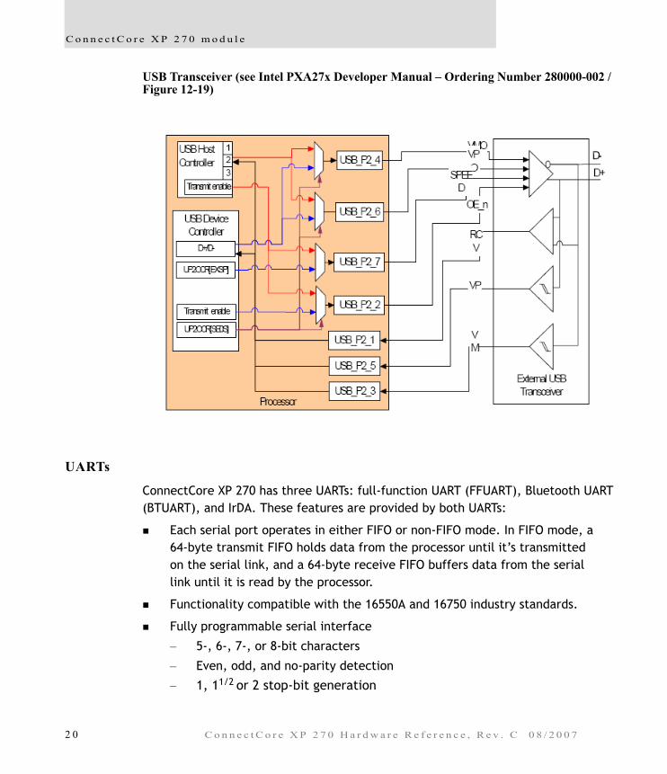
USB Transceiver (see Intel PXA27x Developer Manual – Ordering Number 280000-002 / Figure 12-19)
UARTs
ConnectCore XP 270 has three UARTs: full-function UART (FFUART), Bluetooth UART (BTUART), and IrDA. These features are provided by both UARTs:
Each serial port operates in either FIFO or non-FIFO mode. In FIFO mode, a 64-byte transmit FIFO holds data from the processor until it’s transmitted on the serial link, and a 64-byte receive FIFO buffers data from the serial link until it is read by the processor.
Functionality compatible with the 16550A and 16750 industry standards.
Fully programmable serial interface
– 5-, 6-, 7-, or 8-bit characters
– Even, odd, and no-parity detection
– 1, 11/2 or 2 stop-bit generation
2 0 C o n n e c t C o r e X P 2 7 0 H a r d w a r e R e f e r e n c e , R e v . C 0 8 / 2 0 0 7
A b o u t t h e M o d u l e
– Baud-rate generation up to 921 kbps for all UARTs
– False start-bit detection
Separate DMA requests for transmit and receive data services
SSP Serial Ports
ConnectCore XP 270 supports two Synchronous Serial Protocol serial ports (SSP and NSSP). The SSP ports are a synchronous serial interfaces that connect to a variety of external analog-to- digital (A/D) converters, audio and telecommunication codecs, and many other devices that use serial protocols for data transfer. The SSP ports provide support for these protocols:
Texas Instruments (TI) Synchronous Serial Protocol
Motorola Serial Peripheral Interface (SPI) protocol
National Semiconductor Microwire
Programmable Serial Protocol (PSP)
The SSP ports operate as full-duplex devices for TI Synchronous Serial Protocol, SPI and PSP protocols and as a half-duplex device for the Microwire protocol.
The FIFO can be loaded or emptied by the CPU using programmed I/O or by DMA burst transfers.
Features
One transmit FIFO and one receive FIFO, each 16 samples deep by 32-bits wide
Sample sizes from 4- to 32-bits
Bit-rates from 6.3 Kbps (minimum) to 13 Mbps (maximum)
Master-mode and slave-mode operation
Receive-without-transmit operation
Network mode with up to eight time slots and independent transmit/receive in any/all/none of the time slots — available only with TI Synchronous Serial Protocol and Programmable Serial Protocol (PSP) formats
Audio clock control to provide a 4x output clock and support for selection of most standard audio Codec frequencies
w w w . d i g i . c o m 2 1
C o n n e c t C o r e X P 2 7 0 m o d u l e
I²C Bus Interface
The PXA270 processor has two I²C (Inter-Integrated Circuit) peripherals: the standard I²C interface and the power-manager interface (a subset of the standard I²C interface). Only the standard I²C bus is available externally on the module. The power I²C bus is used for controlling the PMIC (Power Management IC).
The I²C interface allows the ConnectCore XP 270 to serve as a master and a slave device on the I²C bus.
Features
I²C compliant (see the I²C Bus Specification, Version 2.0)
Multi-master and arbitration support
Standard-speed operation @ 100 kbps. Power-I²C standard-speed operation is 40 kbps.
Fast-mode operation @ 400 kbps. Power-I²C fast-mode operation is 160 kbps.
PC Card and CompactFlash Interface
The PC Card interface conforms to the PC Card Standard, Volume 2, Electrical Specification, Version 1.4 and CF+ and CompactFlash Specification Version 1.4. The PC Card and CompactFlash interfaces provide control signals to support one or two PC or CompactFlash card slots.
Features
8- or 16-bit transfer possibilities
Any combination of PC Card and CompactFlash can be used for the two PC Card sockets.
The PC Card interface supports 8- and 16-bit peripherals and handles common memory, I/O, and attribute memory accesses.
2 2 C o n n e c t C o r e X P 2 7 0 H a r d w a r e R e f e r e n c e , R e v . C 0 8 / 2 0 0 7
A b o u t t h e M o d u l e
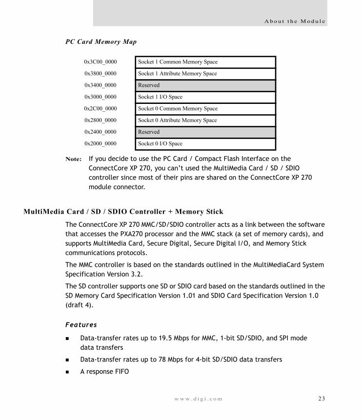
PC Card Memory Map
Note: If you decide to use the PC Card / Compact Flash Interface on the ConnectCore XP 270, you can’t used the MultiMedia Card / SD / SDIO controller since most of their pins are shared on the ConnectCore XP 270 module connector.
MultiMedia Card / SD / SDIO Controller + Memory Stick
The ConnectCore XP 270 MMC/SD/SDIO controller acts as a link between the software that accesses the PXA270 processor and the MMC stack (a set of memory cards), and supports MultiMedia Card, Secure Digital, Secure Digital I/O, and Memory Stick communications protocols.
The MMC controller is based on the standards outlined in the MultiMediaCard System Specification Version 3.2.
The SD controller supports one SD or SDIO card based on the standards outlined in the SD Memory Card Specification Version 1.01 and SDIO Card Specification Version 1.0 (draft 4).
Features
Data-transfer rates up to 19.5 Mbps for MMC, 1-bit SD/SDIO, and SPI mode data transfers
Data-transfer rates up to 78 Mbps for 4-bit SD/SDIO data transfers
A response FIFO
0x3C00_0000 Socket 1 Common Memory Space
0x3800_0000 Socket 1 Attribute Memory Space
0x3400_0000 Reserved
0x3000_0000 Socket 1 I/O Space
0x2C00_0000 Socket 0 Common Memory Space
0x2800_0000 Socket 0 Attribute Memory Space
0x2400_0000 Reserved
0x2000_0000 Socket 0 I/O Space
w w w . d i g i . c o m 2 3
C o n n e c t C o r e X P 2 7 0 m o d u l e
Two transmit FIFOs and two receive FIFOs
Two modes of operation: MMC/SD/SDIO mode and SPI mode. MMC/SD/SDIO mode support MMC, SD, and SDIO communications protocols. SPI mode supports the SPI communications protocol.
1- and 4- bit data transfers are supported for SD and SDIO communications protocols
Controller turns clock on and off, based on status of FIFOs, to prevent overflows and underruns
Support for all valid MMC and SD/SDIO protocol data-transfer modes
Interrupt-based application interface to control software interaction
Support for multiple MMC cards, using the MMC communications protocol
Support for one SD or SDIO card, using the SD or SDIO communications protocol
Support for up to two MMC or SD/SDIO cards, using the SPI communications protocol. Mixed card types are supported for the SPI communications protocol only.
Note: If you decide to use MultiMedia Card / SD / SDIO controller on the ConnectCore XP 270, you can’t use PC Card / Compact Flash Interface since most of their pins are shared on the ConnectCore XP 270 module connector.
LCD Controller
The LCD controller provides an interface between the PXA270 processor and a flat-panel display module. The flat-panel display module can be passive (DSTN), active (TFT), or an LCD panel with internal frame buffering (smart panels).
The LCD/flat-panel controller is backward-compatible with Intel PXA250 processor LCD controllers.
Features
Single- or dual-scan display modules
Up to 256 gray-scale levels (8 bits) in passive monochrome mode
Up to 16777216 colors (24 bits) in active color mode
2 4 C o n n e c t C o r e X P 2 7 0 H a r d w a r e R e f e r e n c e , R e v . C 0 8 / 2 0 0 7

A b o u t t h e M o d u l e
A total of 16777216 colors (24 bits) in passive color mode
Up to 8-bit (each) passive dual-scan color displays
Up to 16-bit per pixel for active single-panel color displays
Up to 24-bit per pixel single-panel color smart panels
Support for display sizes from 1x1 to 800x600 pixels
LCD controller contains a 64-entry x 24-bit wide output FIFO that stores pixel pin data before it is driven out to the pins
Overlays supported with pixel depths of 16, 24 and 25 bpp in RGBT format
Provides one base layer plus two overlays for single-scan displays; maximum size of each overlay can equal the display size
Hardware support for color-space conversion from YCbCr to RGB for video streams
Support hardware cursor for single-scan display
Programmable pixel clock from 52.0 MHz to 25.4 kHz
Supports little-endian ordering of pixels in frame buffer
Programmable interrupts for input and output FIFOs (underrun)
The color depth determines the number of pins used. All 16 bpp active displays require 16 data lines. All 18 bpp active displays require 18 data lines. Only with 24 bpp does the PXA270 processor use a different number of pins than the color depth; the processor outputs the data on 8 lines.
Note: ConnectCore XP 270 only supports externally a 16-bit LCD data bus. LCD[17] and LCD[16] aren’t routed on the module’s connector due to place availability on the connector. That means it’s impossible to implement 18bpp displays with ConnectCore XP 270.
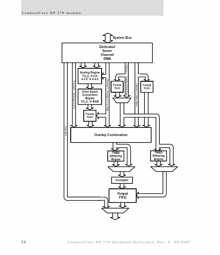
The next diagram shows the Intel PXA270 LCD Controller Unit. For more information, see “Intel PXA27x Processor Family Developer’s Manual – Order Number: 280000-002”.
w w w . d i g i . c o m 2 5
C o n n e c t C o r e X P 2 7 0 m o d u l e
2 6 C o n n e c t C o r e X P 2 7 0 H a r d w a r e R e f e r e n c e , R e v . C 0 8 / 2 0 0 7
A b o u t t h e M o d u l e
AC’97 Controller
The ConnectCore XP 270 AC’97 controller supports the “Audio Codec ’97 Component Specification, Revision 2.0”. The AC-link is a synchronous, fixed-rate serial bus interface to the digital AC’97 controller for transferring digital audio, modem, microphone input (MIC-in), Codec register control, and status information.
Features
Independent channels for stereo pulse code modulation (PCM) in, stereo PCM out, modem out, modem-in, and mono MIC-in. All of the channels support only 16-bit samples in hardware. Samples less than 16 bits are supported through software.
Multiple sample rate AC’97 2.0 Codecs (48 kHz and below). The AC’97 controller depends on the Codec to control the varying rate.
Secondary Codec support
Three receive FIFOs (32-bit, 16 entries)
Two transmit FIFOs (32-bit, 16 entries)
Optional AC97_SYSCLK output (support for Codecs without oscillators or crystals)
The AC’97 controller does not support the following optional AC’97 Revision 2.0 features:
Double-rate sampling (n+1 sample for PCM L, R and C)
18- and 20-bit sample lengths
Pulse Width Modulator Controller
ConnectCore XP 270 provides two PWM outputs. Each PWM operates independently of the other. In general, the PWM controller provides a basic digital-to-analog converter with an appropriate analog filter; for example, controlling the brightness of an LED output or controlling LCD contrast.
w w w . d i g i . c o m 2 7
C o n n e c t o r p i n o u t
Features (short list):
Enhanced period control through 6-bit clock divider and 10-bit period counter
10-bit pulse control
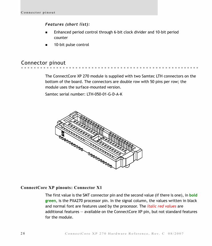
Connector pinout
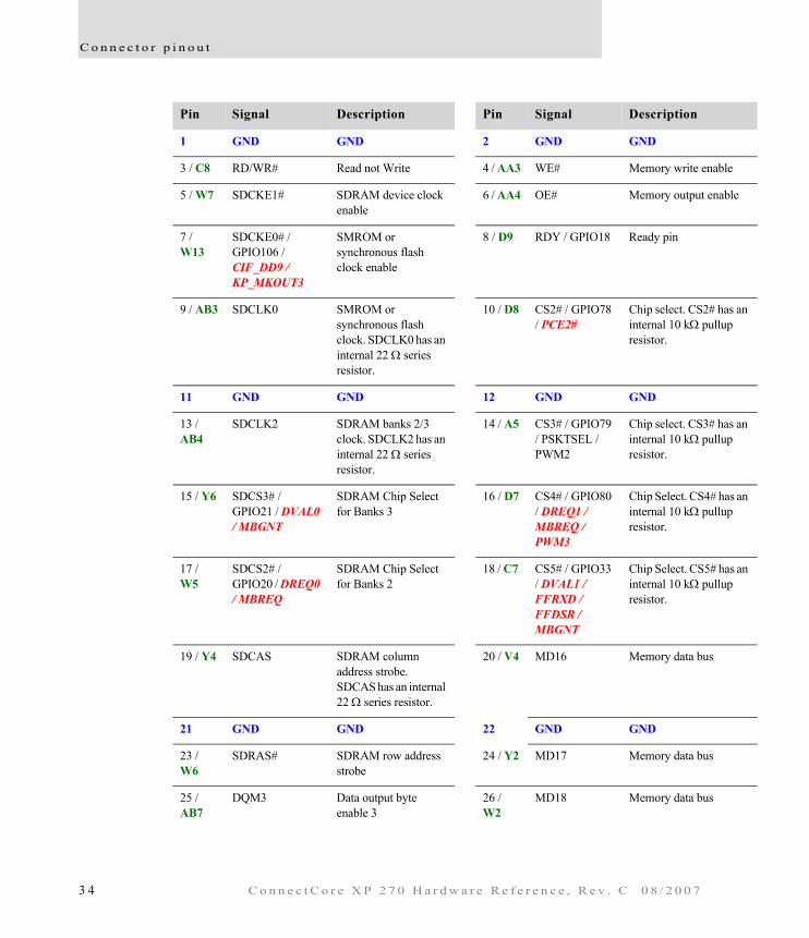
The ConnectCore XP 270 module is supplied with two Samtec LTH connectors on the bottom of the board. The connectors are double row with 50 pins per row; the module uses the surface-mounted version.
Samtec serial number: LTH-050-01-G-D-A-K
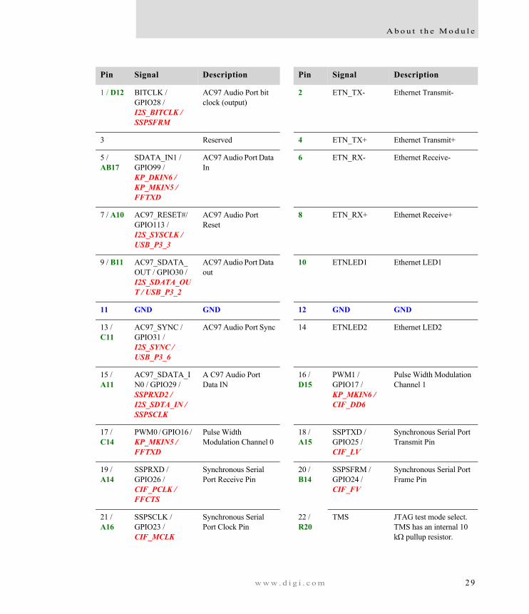
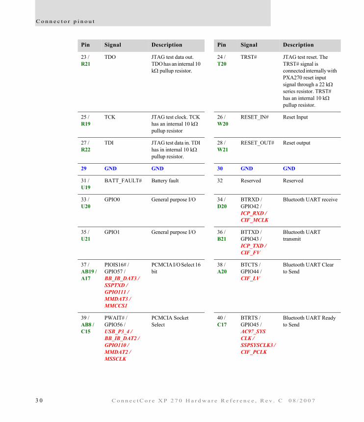
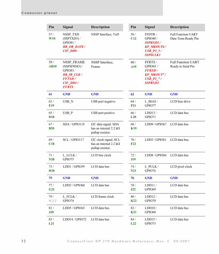
ConnectCore XP pinouts: Connector X1
The first value is the SMT connector pin and the second value (if there is one), in bold green, is the PXA270 processor pin. In the signal column, the values written in black and normal font are features used by the processor. The italic red values are additional features — available on the ConnectCore XP pin, but not standard features for the module.
2 8 C o n n e c t C o r e X P 2 7 0 H a r d w a r e R e f e r e n c e , R e v . C 0 8 / 2 0 0 7
A b o u t t h e M o d u l e
Pin Signal Description Pin Signal Description
1 / D12 BITCLK / GPIO28 / I2S_BITCLK / SSPSFRM
AC97 Audio Port bit clock (output)
2 ETN_TX- Ethernet Transmit-
3 Reserved 4 ETN_TX+ Ethernet Transmit+
5 / AB17
SDATA_IN1 / GPIO99 / KP_DKIN6 / KP_MKIN5 / FFTXD
AC97 Audio Port Data In
6 ETN_RX- Ethernet Receive-
7 / A10 AC97_RESET#/ GPIO113 / I2S_SYSCLK / USB_P3_3
AC97 Audio Port Reset
8 ETN_RX+ Ethernet Receive+
9 / B11 AC97_SDATA_OUT / GPIO30 / I2S_SDATA_OUT / USB_P3_2
AC97 Audio Port Data out
10 ETNLED1 Ethernet LED1
11 GND GND 12 GND GND
13 / C11
AC97_SYNC / GPIO31 / I2S_SYNC / USB_P3_6
AC97 Audio Port Sync 14 ETNLED2 Ethernet LED2
15 / A11
AC97_SDATA_IN0 / GPIO29 / SSPRXD2 / I2S_SDTA_IN / SSPSCLK
A C97 Audio Port Data IN
16 / D15
PWM1 / GPIO17 / KP_MKIN6 / CIF_DD6
Pulse Width Modulation Channel 1
17 / C14
PWM0 / GPIO16 / KP_MKIN5 / FFTXD
Pulse Width Modulation Channel 0
18 / A15
SSPTXD / GPIO25 / CIF_LV
Synchronous Serial Port Transmit Pin
19 / A14
SSPRXD / GPIO26 / CIF_PCLK / FFCTS
Synchronous Serial Port Receive Pin
20 / B14
SSPSFRM / GPIO24 / CIF_FV
Synchronous Serial Port Frame Pin
21 / A16
SSPSCLK / GPIO23 / CIF_MCLK
Synchronous Serial Port Clock Pin
22 / R20
TMS JTAG test mode select. TMS has an internal 10 kΩ pullup resistor.
w w w . d i g i . c o m 2 9
C o n n e c t o r p i n o u t
23 / R21
TDO JTAG test data out. TDO has an internal 10 kΩ pullup resistor.
24 / T20
TRST# JTAG test reset. The TRST# signal is connected internally with PXA270 reset input signal through a 22 kΩ series resistor. TRST# has an internal 10 kΩ pullup resistor.
25 / R19
TCK JTAG test clock. TCK has an internal 10 kΩ pullup resistor
26 / W20
RESET_IN# Reset Input
27 / R22
TDI JTAG test data in. TDI has in internal 10 kΩ pullup resistor.
28 / W21
RESET_OUT# Reset output
29 GND GND 30 GND GND
31 / U19
BATT_FAULT# Battery fault 32 Reserved Reserved
33 / U20
GPIO0 General purpose I/O 34 / D20
BTRXD / GPIO42 / ICP_RXD / CIF_MCLK
Bluetooth UART receive
35 / U21
GPIO1 General purpose I/O 36 / B21
BTTXD / GPIO43 / ICP_TXD / CIF_FV
Bluetooth UART transmit
37 / AB19 / A17
PIOIS16# / GPIO57 / BB_IB_DAT3 / SSPTXD /GPIO111 / MMDAT3 / MMCCS1
PCMCIA I/O Select 16 bit
38 / A20
BTCTS / GPIO44 / CIF_LV
Bluetooth UART Clear to Send
39 / AB8 / C15
PWAIT# / GPIO56 / USB_P3_4 / BB_IB_DAT2 / GPIO110 / MMDAT2 / MSSCLK
PCMCIA Socket Select
40 / C17
BTRTS / GPIO45 /AC97_SYSCLK / SSPSYSCLK3 / CIF_PCLK
Bluetooth UART Ready to Send
Pin Signal Description Pin Signal Description
3 0 C o n n e c t C o r e X P 2 7 0 H a r d w a r e R e f e r e n c e , R e v . C 0 8 / 2 0 0 7
A b o u t t h e M o d u l e
41 / W14 / C16
PSKTSEL / GPIO104 / CIF_DD2 / KP_MKOUT1 / GPIO32 / MMCLK / MSSCLK
PCMCIA socket select 42 / AA12
FFRXD / GPIO53 / USB_P2_3 / BB_OB_STB / CIF_MCLK / SSPSYSCLK
Full function UART receive pin
43 / AB12 / A18
PIOW# / GPIO51 / CIF_DD2 / BB_OB_DAT3 / GPIO92 / MMDAT0 / MSBS
PCMCIA I/O Write 44 / B17
FFTXD / GPIO39 / KP_MKIN4 / USB_P2_6 / SSPSFRM3
Full function UART transmit pin
45 / AB13
PCE2# / GPIO54 / CIF_PCLK / BB_OB_WAIT
PCMCIA high byte enable. PCE2# has an internal 10 kΩ pullup resistor.
46 / B13
FFDCD / GPIO36 / USB_P2_4 / SSPSCLK2 / KP_MKIN7
Full function UART Carrier Detect pin
47 / W12 / B16
PIOR# / GPIO50 / CIF_DD3 / BB_OB_DAT2 / SSPSCLK2 / GPIO112 / MMCMD / MSINS#
PCMCIA I/O read 48 / D17
FFCTS / GPIO35 / USB_P2_1 / KP _MKOUT6 / SSPTXD3 / SSPSFRMS
Full function UART Clear to Send pin
49 +3.3V Power supply 50 +3.3V Power supply
51 +3.3V Power supply 52 +3.3V Power supply
53 / AA8
NSSP_RXD (SSPRXD3) / GPIO82 / BB_IB_DAT0 / CIF_DD5 / FFDTR
NSSP Interface, RxD 54 / A13
FFRI / GPIO38 SSPTXD3 / KP_MKIN4 / SSPTXD2 / USB_P2_3 / PWM1
Full Function UART Ring Indicator Pin
55 / Y10
NSSP_CLK (SSPSCLK3 / GPIO84 / BB_IB_STB / CIF_FV
NSSP Interface, CLK 56 / D13
FFDSR / GPIO37 / USB_P2_8 / SSPSFRM2 / KP_MKIN3 / FFTXD
Full Function UART Data Set Ready Pin
Pin Signal Description Pin Signal Description
w w w . d i g i . c o m 3 1
C o n n e c t o r p i n o u t
57 / W10
NSSP_TXD (SSPTXD3) / GPIO81 / BB_OB_DAT0 / CIF_DD0
NSSP Interface, TxD 58 / C12
FFDTR / GPIO40 / SSPRXD2 / KP_MKOUT6 / USB_P2_5 / SSPSCLK3
Full Function UART Data Term Ready Pin
59 / AB10
NSSP_FRAME (SSPSFRM3) / GPIO83 / BB_IB_CLK / FFTXD / CIF_DD4 / FFRTS
NSSP Interface, Frame
60 / A19
FFRTS / GPIO41 / FFRXD / KP_MKOUT7 / USB_P2_7 / SSPRXD3
Full Function UART Ready to Send Pin
61 GND GND 62 GND GND
63 / E19
USB_N USB port negative 64 / P21
L_BIAS / GPIO77
LCD bias drive
65 / D18
USB_P USB port positive 66 / L20
LDD13 / GPIO71
LCD data bus
67 / B20
SDA / GPIO118 I2C data signal. SDA has an internal 2.2 kΩ pullup resistor.
68 / K19
LDD9 / GPIO67 LCD data bus
69 / C18
SCL / GPIO117 I2C clock signal. SCL has an internal 2.2 kΩ pullup resistor.
70 / F22
LDD3 / GPIO61 LCD data bus.
71 / N20
L_LCLK / GPIO75
LCD line clock 72 / J19
LDD8 / GPIO66 LCD data bus
73 / H20
LDD1 / GPIO59 LCD data bus 74 / N21
L_PCLK / GPIO76
LCD pixel clock
75 GND GND 76 GND GND
77 / G21
LDD2 / GPIO60 LCD data bus 78 / J22
LDD11 / GPIO69
LCD data bus
79 / N 2 2
L_FCLK / GPIO74
LCD frame clock 80 / K22
LDD12 / GPIO70
LCD data bus
81 / J20
LDD5 / GPIO63 LCD data bus 82 / K21
LDD10 / GPIO68
LCD data bus
83 / L21
LDD14 / GPIO72 LCD data bus 84 / L22
LDD15 / GPIO73
LCD data bus
Pin Signal Description Pin Signal Description
3 2 C o n n e c t C o r e X P 2 7 0 H a r d w a r e R e f e r e n c e , R e v . C 0 8 / 2 0 0 7
A b o u t t h e M o d u l e
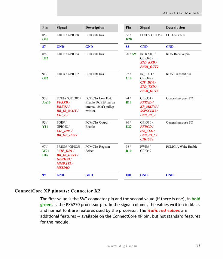
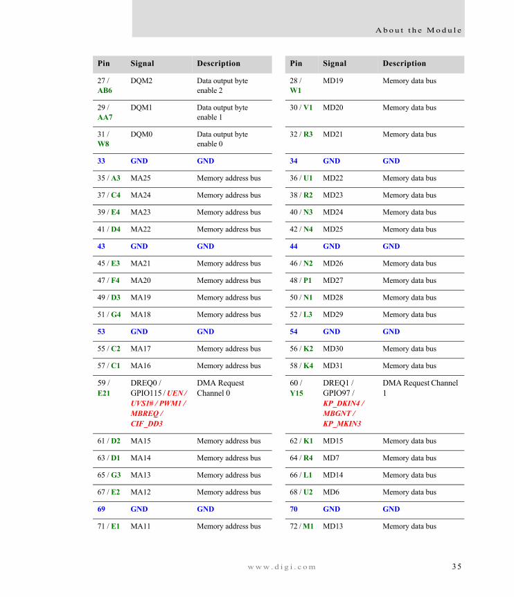
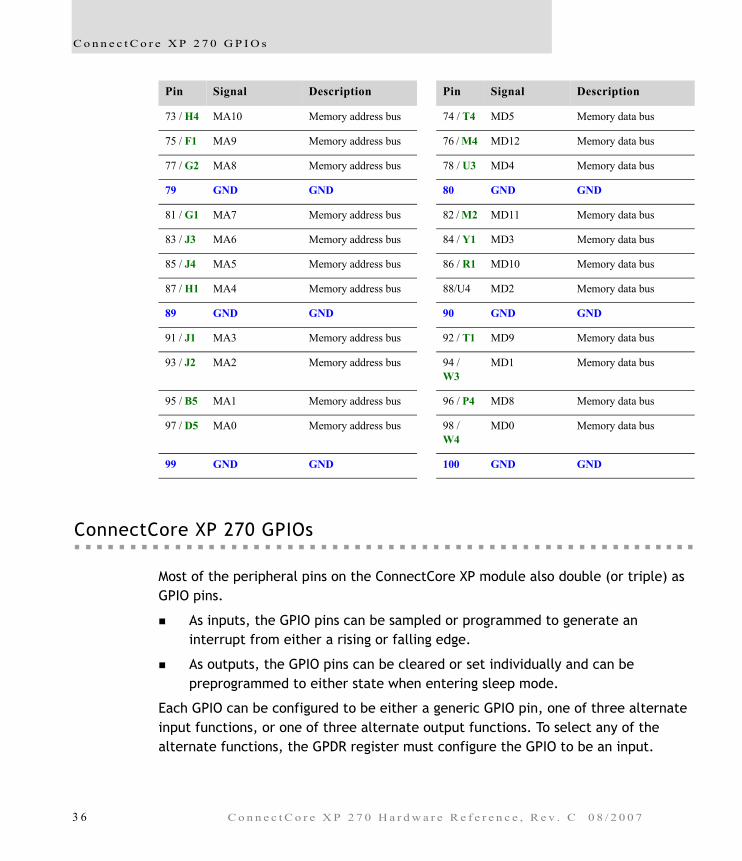
ConnectCore XP pinouts: Connector X2
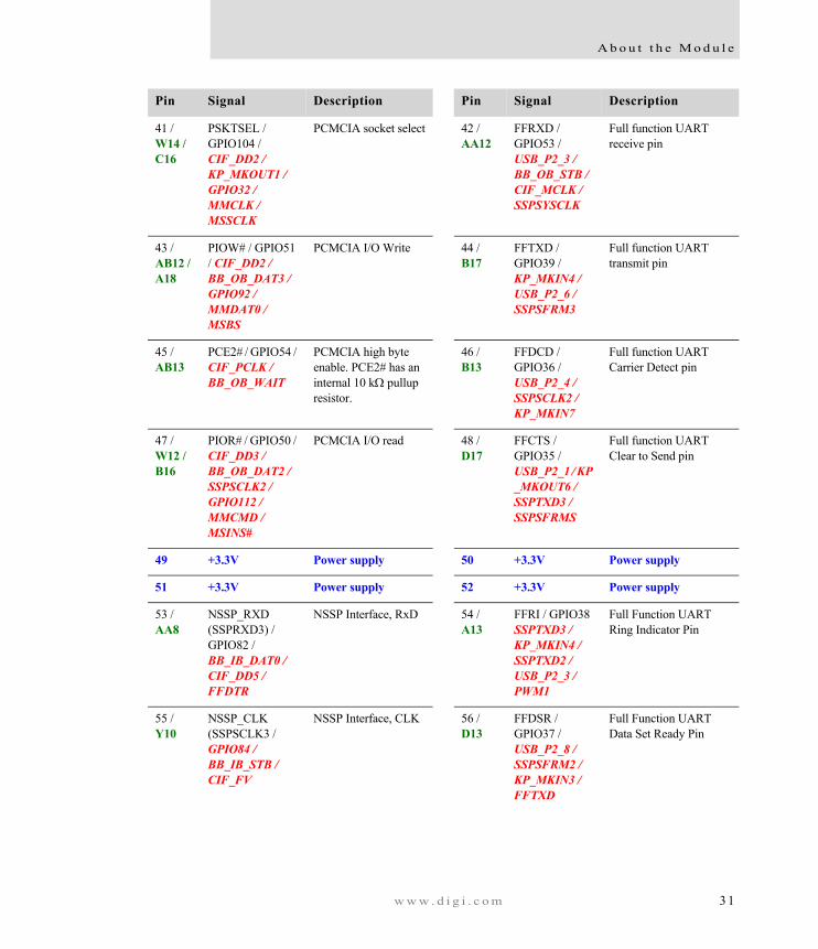
The first value is the SMT connector pin and the second value (if there is one), in bold green, is the PXA270 processor pin. In the signal column, the values written in black and normal font are features used by the processor. The italic red values are additional features — available on the ConnectCore XP pin, but not standard features for the module.
85 / G20
LDD0 / GPIO58 LCD data bus 86 / K20
LDD7 / GPIO65 LCD data bus
87 GND GND 88 GND GND
89 / H22
LDD6 / GPIO64 LCD data bus 90 / A9 IR_RXD_ /GPIO46 / STD_RXD / PWM_OUT2
IrDA Receive pin
91 / G22
LDD4 / GPIO62 LCD data bus 92 / C10
IR_TXD / GPIO47 / CIF_DD0 / STD_TXD / PWM_OUT3
IrDA Transmit pin
93 / AA10
PCE1# / GPIO85 / FFRXD / DREQ2 / BB_IB_WAIT / CIF_LV
PCMCIA Low Byte Enable. PCE1# has an internal 10 kΩ pullup resistor.
94 / B19
GPIO34 / FFRXD / KP_MKIN3 / SSPSCLK3 / USB_P2_2
General purpose I/O
95 / Y11
POE# / GPIO48 / CIF_DD5 / BB_OB_DAT1
PCMCIA Output Enable
96 / U22
GPIO10 / FFDCD / HZ_CLK / USB_P3_5 / CHOUT1
General purpose I/O
97 / W9 / D16
PREG# / GPIO55 / CIF_DD1 / BB_IB_DAT1 / GPIO109 / MMDAT1 / MSSDIO
PCMCIA Register Select
98 / D10
PWE# / GPIO49
PCMCIA Write Enable
99 GND GND 100 GND GND
Pin Signal Description Pin Signal Description
w w w . d i g i . c o m 3 3
C o n n e c t o r p i n o u t
Pin Signal Description Pin Signal Description
1 GND GND 2 GND GND
3 / C8 RD/WR# Read not Write 4 / AA3 WE# Memory write enable
5 / W7 SDCKE1# SDRAM device clock enable
6 / AA4 OE# Memory output enable
7 / W13
SDCKE0# / GPIO106 / CIF_DD9 / KP_MKOUT3
SMROM or synchronous flash clock enable
8 / D9 RDY / GPIO18 Ready pin
9 / AB3 SDCLK0 SMROM or synchronous flash clock. SDCLK0 has an internal 22 Ω series resistor.
10 / D8 CS2# / GPIO78 / PCE2#
Chip select. CS2# has an internal 10 kΩ pullup resistor.
11 GND GND 12 GND GND
13 / AB4
SDCLK2 SDRAM banks 2/3 clock. SDCLK2 has an internal 22 Ω series resistor.
14 / A5 CS3# / GPIO79 / PSKTSEL / PWM2
Chip select. CS3# has an internal 10 kΩ pullup resistor.
15 / Y6 SDCS3# / GPIO21 / DVAL0 / MBGNT
SDRAM Chip Select for Banks 3
16 / D7 CS4# / GPIO80 / DREQ1 / MBREQ / PWM3
Chip Select. CS4# has an internal 10 kΩ pullup resistor.
17 / W5
SDCS2# / GPIO20 / DREQ0 / MBREQ
SDRAM Chip Select for Banks 2
18 / C7 CS5# / GPIO33 / DVAL1 / FFRXD / FFDSR / MBGNT
Chip Select. CS5# has an internal 10 kΩ pullup resistor.
19 / Y4 SDCAS SDRAM column address strobe. SDCAS has an internal 22 Ω series resistor.
20 / V4 MD16 Memory data bus
21 GND GND 22 GND GND
23 / W6
SDRAS# SDRAM row address strobe
24 / Y2 MD17 Memory data bus
25 / AB7
DQM3 Data output byte enable 3
26 / W2
MD18 Memory data bus
3 4 C o n n e c t C o r e X P 2 7 0 H a r d w a r e R e f e r e n c e , R e v . C 0 8 / 2 0 0 7
A b o u t t h e M o d u l e
27 / AB6
DQM2 Data output byte enable 2
28 / W1
MD19 Memory data bus
29 / AA7
DQM1 Data output byte enable 1
30 / V1 MD20 Memory data bus
31 / W8
DQM0 Data output byte enable 0
32 / R3 MD21 Memory data bus
33 GND GND 34 GND GND
35 / A3 MA25 Memory address bus 36 / U1 MD22 Memory data bus
37 / C4 MA24 Memory address bus 38 / R2 MD23 Memory data bus
39 / E4 MA23 Memory address bus 40 / N3 MD24 Memory data bus
41 / D4 MA22 Memory address bus 42 / N4 MD25 Memory data bus
43 GND GND 44 GND GND
45 / E3 MA21 Memory address bus 46 / N2 MD26 Memory data bus
47 / F4 MA20 Memory address bus 48 / P1 MD27 Memory data bus
49 / D3 MA19 Memory address bus 50 / N1 MD28 Memory data bus
51 / G4 MA18 Memory address bus 52 / L3 MD29 Memory data bus
53 GND GND 54 GND GND
55 / C2 MA17 Memory address bus 56 / K2 MD30 Memory data bus
57 / C1 MA16 Memory address bus 58 / K4 MD31 Memory data bus
59 / E21
DREQ0 / GPIO115 / UEN / UVS1# / PWM1 / MBREQ / CIF_DD3
DMA Request Channel 0
60 / Y15
DREQ1 / GPIO97 / KP_DKIN4 / MBGNT / KP_MKIN3
DMA Request Channel 1
61 / D2 MA15 Memory address bus 62 / K1 MD15 Memory data bus
63 / D1 MA14 Memory address bus 64 / R4 MD7 Memory data bus
65 / G3 MA13 Memory address bus 66 / L1 MD14 Memory data bus
67 / E2 MA12 Memory address bus 68 / U2 MD6 Memory data bus
69 GND GND 70 GND GND
71 / E1 MA11 Memory address bus 72 / M1 MD13 Memory data bus
Pin Signal Description Pin Signal Description
w w w . d i g i . c o m 3 5
C o n n e c t C o r e X P 2 7 0 G P I O s
ConnectCore XP 270 GPIOs
Most of the peripheral pins on the ConnectCore XP module also double (or triple) as GPIO pins.
As inputs, the GPIO pins can be sampled or programmed to generate an interrupt from either a rising or falling edge.
As outputs, the GPIO pins can be cleared or set individually and can be preprogrammed to either state when entering sleep mode.
Each GPIO can be configured to be either a generic GPIO pin, one of three alternate input functions, or one of three alternate output functions. To select any of the alternate functions, the GPDR register must configure the GPIO to be an input.
73 / H4 MA10 Memory address bus 74 / T4 MD5 Memory data bus
75 / F1 MA9 Memory address bus 76 / M4 MD12 Memory data bus
77 / G2 MA8 Memory address bus 78 / U3 MD4 Memory data bus
79 GND GND 80 GND GND
81 / G1 MA7 Memory address bus 82 / M2 MD11 Memory data bus
83 / J3 MA6 Memory address bus 84 / Y1 MD3 Memory data bus
85 / J4 MA5 Memory address bus 86 / R1 MD10 Memory data bus
87 / H1 MA4 Memory address bus 88/U4 MD2 Memory data bus
89 GND GND 90 GND GND
91 / J1 MA3 Memory address bus 92 / T1 MD9 Memory data bus
93 / J2 MA2 Memory address bus 94 / W3
MD1 Memory data bus
95 / B5 MA1 Memory address bus 96 / P4 MD8 Memory data bus
97 / D5 MA0 Memory address bus 98 / W4
MD0 Memory data bus
99 GND GND 100 GND GND
Pin Signal Description Pin Signal Description
3 6 C o n n e c t C o r e X P 2 7 0 H a r d w a r e R e f e r e n c e , R e v . C 0 8 / 2 0 0 7
A b o u t t h e M o d u l e
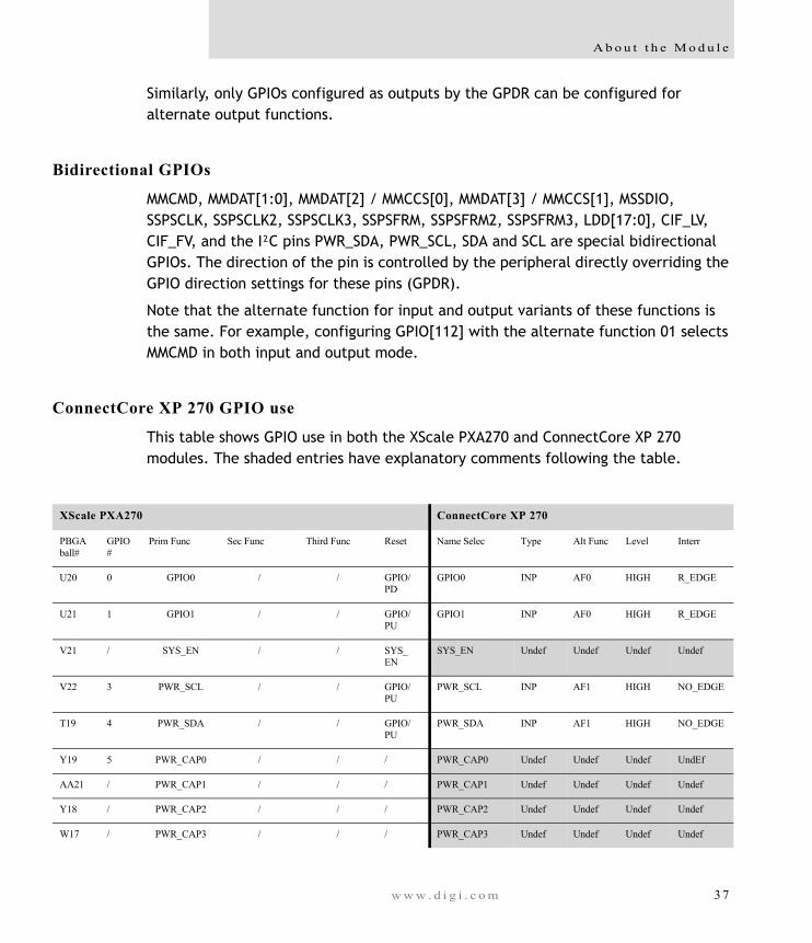
Similarly, only GPIOs configured as outputs by the GPDR can be configured for alternate output functions.
Bidirectional GPIOs
MMCMD, MMDAT[1:0], MMDAT[2] / MMCCS[0], MMDAT[3] / MMCCS[1], MSSDIO, SSPSCLK, SSPSCLK2, SSPSCLK3, SSPSFRM, SSPSFRM2, SSPSFRM3, LDD[17:0], CIF_LV, CIF_FV, and the I²C pins PWR_SDA, PWR_SCL, SDA and SCL are special bidirectional GPIOs. The direction of the pin is controlled by the peripheral directly overriding the GPIO direction settings for these pins (GPDR).
Note that the alternate function for input and output variants of these functions is the same. For example, configuring GPIO[112] with the alternate function 01 selects MMCMD in both input and output mode.
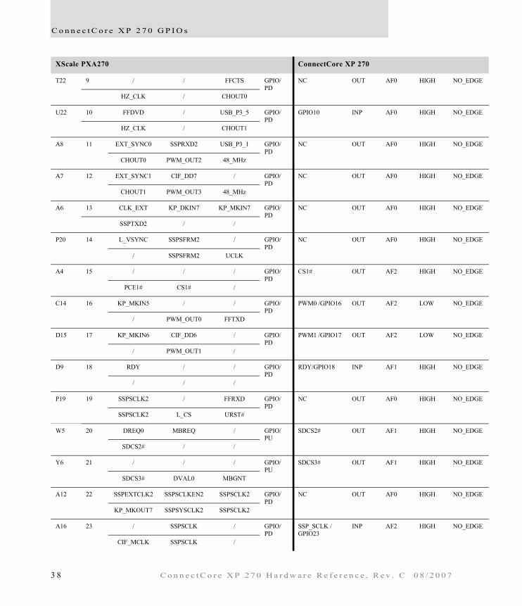
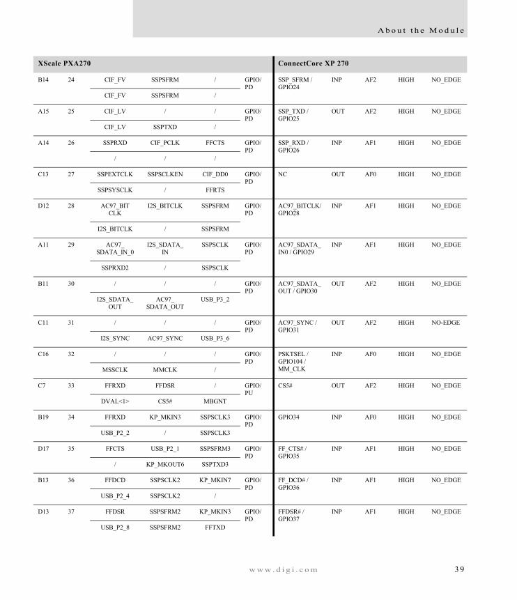
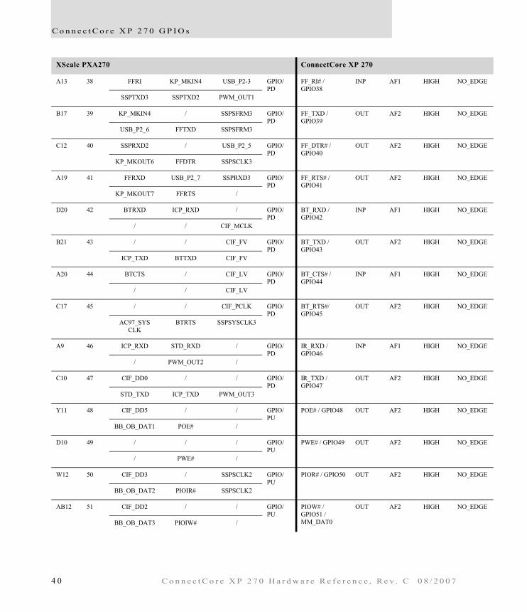
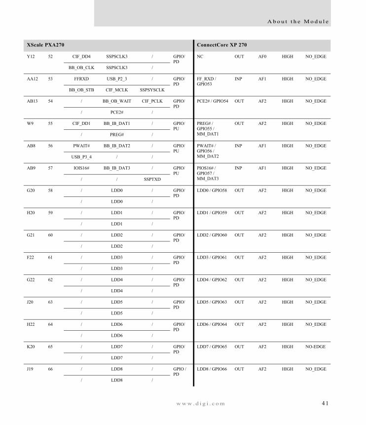
ConnectCore XP 270 GPIO use
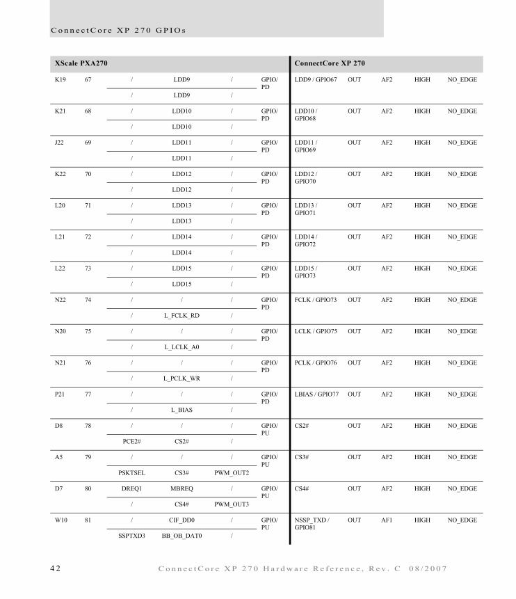
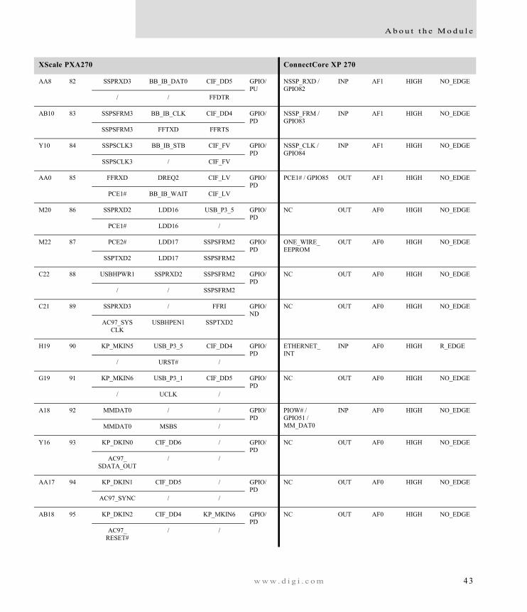
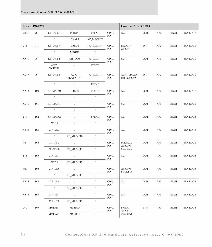
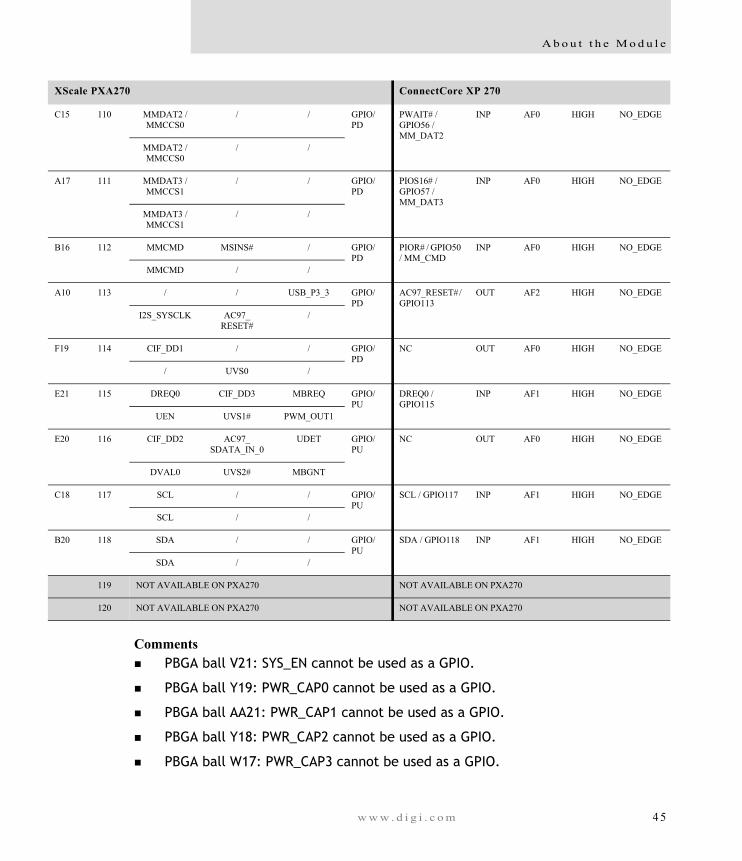
This table shows GPIO use in both the XScale PXA270 and ConnectCore XP 270 modules. The shaded entries have explanatory comments following the table.
XScale PXA270 ConnectCore XP 270
PBGA ball#
GPIO #
Prim Func Sec Func Third Func Reset Name Selec Type Alt Func Level Interr
U20 0 GPIO0 / / GPIO/PD
GPIO0 INP AF0 HIGH R_EDGE
U21 1 GPIO1 / / GPIO/PU
GPIO1 INP AF0 HIGH R_EDGE
V21 / SYS_EN / / SYS_EN
SYS_EN Undef Undef Undef Undef
V22 3 PWR_SCL / / GPIO/PU
PWR_SCL INP AF1 HIGH NO_EDGE
T19 4 PWR_SDA / / GPIO/PU
PWR_SDA INP AF1 HIGH NO_EDGE
Y19 5 PWR_CAP0 / / / PWR_CAP0 Undef Undef Undef UndEf
AA21 / PWR_CAP1 / / / PWR_CAP1 Undef Undef Undef Undef
Y18 / PWR_CAP2 / / / PWR_CAP2 Undef Undef Undef Undef
W17 / PWR_CAP3 / / / PWR_CAP3 Undef Undef Undef Undef
w w w . d i g i . c o m 3 7
C o n n e c t C o r e X P 2 7 0 G P I O s
T22 9 / / FFCTS GPIO/PD
NC OUT AF0 HIGH NO_EDGE
HZ_CLK / CHOUT0
U22 10 FFDVD / USB_P3_5 GPIO/PD
GPIO10 INP AF0 HIGH NO_EDGE
HZ_CLK / CHOUT1
A8 11 EXT_SYNC0 SSPRXD2 USB_P3_1 GPIO/PD
NC OUT AF0 HIGH NO_EDGE
CHOUT0 PWM_OUT2 48_MHz
A7 12 EXT_SYNC1 CIF_DD7 / GPIO/PD
NC OUT AF0 HIGH NO_EDGE
CHOUT1 PWM_OUT3 48_MHz
A6 13 CLK_EXT KP_DKIN7 KP_MKIN7 GPIO/PD
NC OUT AF0 HIGH NO_EDGE
SSPTXD2 / /
P20 14 L_VSYNC SSPSFRM2 / GPIO/PD
NC OUT AF0 HIGH NO_EDGE
/ SSPSFRM2 UCLK
A4 15 / / / GPIO/PD
CS1# OUT AF2 HIGH NO_EDGE
PCE1# CS1# /
C14 16 KP_MKIN5 / / GPIO/PD
PWM0 /GPIO16 OUT AF2 LOW NO_EDGE
/ PWM_OUT0 FFTXD
D15 17 KP_MKIN6 CIF_DD6 / GPIO/PD
PWM1 /GPIO17 OUT AF2 LOW NO_EDGE
/ PWM_OUT1 /
D9 18 RDY / / GPIO/PD
RDY/GPIO18 INP AF1 HIGH NO_EDGE
/ / /
P19 19 SSPSCLK2 / FFRXD GPIO/PD
NC OUT AF0 HIGH NO_EDGE
SSPSCLK2 L_CS URST#
W5 20 DREQ0 MBREQ / GPIO/PU
SDCS2# OUT AF1 HIGH NO_EDGE
SDCS2# / /
Y6 21 / / / GPIO/PU
SDCS3# OUT AF1 HIGH NO_EDGE
SDCS3# DVAL0 MBGNT
A12 22 SSPEXTCLK2 SSPSCLKEN2 SSPSCLK2 GPIO/PD
NC OUT AF0 HIGH NO_EDGE
KP_MKOUT7 SSPSYSCLK2 SSPSCLK2
A16 23 / SSPSCLK / GPIO/PD
SSP_SCLK /GPIO23
INP AF2 HIGH NO_EDGE
CIF_MCLK SSPSCLK /
XScale PXA270 ConnectCore XP 270
3 8 C o n n e c t C o r e X P 2 7 0 H a r d w a r e R e f e r e n c e , R e v . C 0 8 / 2 0 0 7
A b o u t t h e M o d u l e
B14 24 CIF_FV SSPSFRM / GPIO/PD
SSP_SFRM /GPIO24
INP AF2 HIGH NO_EDGE
CIF_FV SSPSFRM /
A15 25 CIF_LV / / GPIO/PD
SSP_TXD /GPIO25
OUT AF2 HIGH NO_EDGE
CIF_LV SSPTXD /
A14 26 SSPRXD CIF_PCLK FFCTS GPIO/PD
SSP_RXD /GPIO26
INP AF1 HIGH NO_EDGE
/ / /
C13 27 SSPEXTCLK SSPSCLKEN CIF_DD0 GPIO/PD
NC OUT AF0 HIGH NO_EDGE
SSPSYSCLK / FFRTS
D12 28 AC97_BITCLK
I2S_BITCLK SSPSFRM GPIO/PD
AC97_BITCLK/GPIO28
INP AF1 HIGH NO_EDGE
I2S_BITCLK / SSPSFRM
A11 29 AC97_SDATA_IN_0
I2S_SDATA_IN
SSPSCLK GPIO/PD
AC97_SDATA_IN0 / GPIO29
INP AF1 HIGH NO_EDGE
SSPRXD2 / SSPSCLK
B11 30 / / / GPIO/PD
AC97_SDATA_OUT / GPIO30
OUT AF2 HIGH NO_EDGE
I2S_SDATA_OUT
AC97_SDATA_OUT
USB_P3_2
C11 31 / / / GPIO/PD
AC97_SYNC / GPIO31
OUT AF2 HIGH NO-EDGE
I2S_SYNC AC97_SYNC USB_P3_6
C16 32 / / / GPIO/PD
PSKTSEL / GPIO104 / MM_CLK
INP AF0 HIGH NO_EDGE
MSSCLK MMCLK /
C7 33 FFRXD FFDSR / GPIO/PU
CS5# OUT AF2 HIGH NO_EDGE
DVAL<1> CS5# MBGNT
B19 34 FFRXD KP_MKIN3 SSPSCLK3 GPIO/PD
GPIO34 INP AF0 HIGH NO_EDGE
USB_P2_2 / SSPSCLK3
D17 35 FFCTS USB_P2_1 SSPSFRM3 GPIO/PD
FF_CTS# / GPIO35
INP AF1 HIGH NO_EDGE
/ KP_MKOUT6 SSPTXD3
B13 36 FFDCD SSPSCLK2 KP_MKIN7 GPIO/PD
FF_DCD# / GPIO36
INP AF1 HIGH NO_EDGE
USB_P2_4 SSPSCLK2 /
D13 37 FFDSR SSPSFRM2 KP_MKIN3 GPIO/PD
FFDSR# / GPIO37
INP AF1 HIGH NO_EDGE
USB_P2_8 SSPSFRM2 FFTXD
XScale PXA270 ConnectCore XP 270
w w w . d i g i . c o m 3 9
C o n n e c t C o r e X P 2 7 0 G P I O s
A13 38 FFRI KP_MKIN4 USB_P2-3 GPIO/PD
FF_RI# / GPIO38
INP AF1 HIGH NO_EDGE
SSPTXD3 SSPTXD2 PWM_OUT1
B17 39 KP_MKIN4 / SSPSFRM3 GPIO/PD
FF_TXD / GPIO39
OUT AF2 HIGH NO_EDGE
USB_P2_6 FFTXD SSPSFRM3
C12 40 SSPRXD2 / USB_P2_5 GPIO/PD
FF_DTR# / GPIO40
OUT AF2 HIGH NO_EDGE
KP_MKOUT6 FFDTR SSPSCLK3
A19 41 FFRXD USB_P2_7 SSPRXD3 GPIO/PD
FF_RTS# / GPIO41
OUT AF2 HIGH NO_EDGE
KP_MKOUT7 FFRTS /
D20 42 BTRXD ICP_RXD / GPIO/PD
BT_RXD / GPIO42
INP AF1 HIGH NO_EDGE
/ / CIF_MCLK
B21 43 / / CIF_FV GPIO/PD
BT_TXD / GPIO43
OUT AF2 HIGH NO_EDGE
ICP_TXD BTTXD CIF_FV
A20 44 BTCTS / CIF_LV GPIO/PD
BT_CTS# / GPIO44
INP AF1 HIGH NO_EDGE
/ / CIF_LV
C17 45 / / CIF_PCLK GPIO/PD
BT_RTS#/GPIO45
OUT AF2 HIGH NO_EDGE
AC97_SYSCLK
BTRTS SSPSYSCLK3
A9 46 ICP_RXD STD_RXD / GPIO/PD
IR_RXD / GPIO46
INP AF1 HIGH NO_EDGE
/ PWM_OUT2 /
C10 47 CIF_DD0 / / GPIO/PD
IR_TXD / GPIO47
OUT AF2 HIGH NO_EDGE
STD_TXD ICP_TXD PWM_OUT3
Y11 48 CIF_DD5 / / GPIO/PU
POE# / GPIO48 OUT AF2 HIGH NO_EDGE
BB_OB_DAT1 POE# /
D10 49 / / / GPIO/PU
PWE# / GPIO49 OUT AF2 HIGH NO_EDGE
/ PWE# /
W12 50 CIF_DD3 / SSPSCLK2 GPIO/PU
PIOR# / GPIO50 OUT AF2 HIGH NO_EDGE
BB_OB_DAT2 PIOIR# SSPSCLK2
AB12 51 CIF_DD2 / / GPIO/PU
PIOW# / GPIO51 / MM_DAT0
OUT AF2 HIGH NO_EDGE
BB_OB_DAT3 PIOIW# /
XScale PXA270 ConnectCore XP 270
4 0 C o n n e c t C o r e X P 2 7 0 H a r d w a r e R e f e r e n c e , R e v . C 0 8 / 2 0 0 7
A b o u t t h e M o d u l e
Y12 52 CIF_DD4 SSPSCLK3 / GPIO/PD
NC OUT AF0 HIGH NO_EDGE
BB_OB_CLK SSPSCLK3 /
AA12 53 FFRXD USB_P2_3 / GPIO/PD
FF_RXD / GPIO53
INP AF1 HIGH NO_EDGE
BB_OB_STB CIF_MCLK SSPSYSCLK
AB13 54 / BB_OB_WAIT CIF_PCLK GPIO/PD
PCE2# / GPIO54 OUT AF2 HIGH NO_EDGE
/ PCE2# /
W9 55 CIF_DD1 BB_IB_DAT1 / GPIO/PU
PREG# / GPIO55 / MM_DAT1
OUT AF2 HIGH NO_EDGE
/ PREG# /
AB8 56 PWAIT# BB_IB_DAT2 / GPIO/PU
PWAIT# / GPIO56 / MM_DAT2
INP AF1 HIGH NO_EDGE
USB_P3_4 / /
AB9 57 IOIS16# BB_IB_DAT3 / GPIO/PU
PIOS16# / GPIO57 / MM_DAT3
INP AF1 HIGH NO_EDGE
/ / SSPTXD
G20 58 / LDD0 / GPIO/PD
LDD0 / GPIO58 OUT AF2 HIGH NO_EDGE
/ LDD0 /
H20 59 / LDD1 / GPIO/PD
LDD1 / GPIO59 OUT AF2 HIGH NO_EDGE
/ LDD1 /
G21 60 / LDD2 / GPIO/PD
LDD2 / GPIO60 OUT AF2 HIGH NO_EDGE
/ LDD2 /
F22 61 / LDD3 / GPIO/PD
LDD3 / GPIO61 OUT AF2 HIGH NO_EDGE
/ LDD3 /
G22 62 / LDD4 / GPIO/PD
LDD4 / GPIO62 OUT AF2 HIGH NO_EDGE
/ LDD4 /
J20 63 / LDD5 / GPIO/PD
LDD5 / GPIO63 OUT AF2 HIGH NO_EDGE
/ LDD5 /
H22 64 / LDD6 / GPIO/PD
LDD6 / GPIO64 OUT AF2 HIGH NO_EDGE
/ LDD6 /
K20 65 / LDD7 / GPIO/PD
LDD7 / GPIO65 OUT AF2 HIGH NO-EDGE
/ LDD7 /
J19 66 / LDD8 / GPIO /PD
LDD8 / GPIO66 OUT AF2 HIGH NO_EDGE
/ LDD8 /
XScale PXA270 ConnectCore XP 270
w w w . d i g i . c o m 4 1
C o n n e c t C o r e X P 2 7 0 G P I O s
K19 67 / LDD9 / GPIO/PD
LDD9 / GPIO67 OUT AF2 HIGH NO_EDGE
/ LDD9 /
K21 68 / LDD10 / GPIO/PD
LDD10 / GPIO68
OUT AF2 HIGH NO_EDGE
/ LDD10 /
J22 69 / LDD11 / GPIO/PD
LDD11 / GPIO69
OUT AF2 HIGH NO_EDGE
/ LDD11 /
K22 70 / LDD12 / GPIO/PD
LDD12 / GPIO70
OUT AF2 HIGH NO_EDGE
/ LDD12 /
L20 71 / LDD13 / GPIO/PD
LDD13 / GPIO71
OUT AF2 HIGH NO_EDGE
/ LDD13 /
L21 72 / LDD14 / GPIO/PD
LDD14 / GPIO72
OUT AF2 HIGH NO_EDGE
/ LDD14 /
L22 73 / LDD15 / GPIO/PD
LDD15 / GPIO73
OUT AF2 HIGH NO_EDGE
/ LDD15 /
N22 74 / / / GPIO/PD
FCLK / GPIO73 OUT AF2 HIGH NO_EDGE
/ L_FCLK_RD /
N20 75 / / / GPIO/PD
LCLK / GPIO75 OUT AF2 HIGH NO_EDGE
/ L_LCLK_A0 /
N21 76 / / / GPIO/PD
PCLK / GPIO76 OUT AF2 HIGH NO_EDGE
/ L_PCLK_WR /
P21 77 / / / GPIO/PD
LBIAS / GPIO77 OUT AF2 HIGH NO_EDGE
/ L_BIAS /
D8 78 / / / GPIO/PU
CS2# OUT AF2 HIGH NO_EDGE
PCE2# CS2# /
A5 79 / / / GPIO/PU
CS3# OUT AF2 HIGH NO_EDGE
PSKTSEL CS3# PWM_OUT2
D7 80 DREQ1 MBREQ / GPIO/PU
CS4# OUT AF2 HIGH NO_EDGE
/ CS4# PWM_OUT3
W10 81 / CIF_DD0 / GPIO/PU
NSSP_TXD / GPIO81
OUT AF1 HIGH NO_EDGE
SSPTXD3 BB_OB_DAT0 /
XScale PXA270 ConnectCore XP 270
4 2 C o n n e c t C o r e X P 2 7 0 H a r d w a r e R e f e r e n c e , R e v . C 0 8 / 2 0 0 7
A b o u t t h e M o d u l e
AA8 82 SSPRXD3 BB_IB_DAT0 CIF_DD5 GPIO/PU
NSSP_RXD / GPIO82
INP AF1 HIGH NO_EDGE
/ / FFDTR
AB10 83 SSPSFRM3 BB_IB_CLK CIF_DD4 GPIO/PD
NSSP_FRM / GPIO83
INP AF1 HIGH NO_EDGE
SSPSFRM3 FFTXD FFRTS
Y10 84 SSPSCLK3 BB_IB_STB CIF_FV GPIO/PD
NSSP_CLK / GPIO84
INP AF1 HIGH NO_EDGE
SSPSCLK3 / CIF_FV
AA0 85 FFRXD DREQ2 CIF_LV GPIO/PD
PCE1# / GPIO85 OUT AF1 HIGH NO_EDGE
PCE1# BB_IB_WAIT CIF_LV
M20 86 SSPRXD2 LDD16 USB_P3_5 GPIO/PD
NC OUT AF0 HIGH NO_EDGE
PCE1# LDD16 /
M22 87 PCE2# LDD17 SSPSFRM2 GPIO/PD
ONE_WIRE_EEPROM
OUT AF0 HIGH NO_EDGE
SSPTXD2 LDD17 SSPSFRM2
C22 88 USBHPWR1 SSPRXD2 SSPSFRM2 GPIO/PD
NC OUT AF0 HIGH NO_EDGE
/ / SSPSFRM2
C21 89 SSPRXD3 / FFRI GPIO/ND
NC OUT AF0 HIGH NO_EDGE
AC97_SYSCLK
USBHPEN1 SSPTXD2
H19 90 KP_MKIN5 USB_P3_5 CIF_DD4 GPIO/PD
ETHERNET_INT
INP AF0 HIGH R_EDGE
/ URST# /
G19 91 KP_MKIN6 USB_P3_1 CIF_DD5 GPIO/PD
NC OUT AF0 HIGH NO_EDGE
/ UCLK /
A18 92 MMDAT0 / / GPIO/PD
PIOW# / GPIO51 / MM_DAT0
INP AF0 HIGH NO_EDGE
MMDAT0 MSBS /
Y16 93 KP_DKIN0 CIF_DD6 / GPIO/PD
NC OUT AF0 HIGH NO_EDGE
AC97_SDATA_OUT
/ /
AA17 94 KP_DKIN1 CIF_DD5 / GPIO/PD
NC OUT AF0 HIGH NO_EDGE
AC97_SYNC / /
AB18 95 KP_DKIN2 CIF_DD4 KP_MKIN6 GPIO/PD
NC OUT AF0 HIGH NO_EDGE
AC97_RESET#
/ /
XScale PXA270 ConnectCore XP 270
w w w . d i g i . c o m 4 3
C o n n e c t C o r e X P 2 7 0 G P I O s
W16 96 KP_DKIN3 MBREQ FFRXD GPIO/PD
NC OUT AF0 HIGH NO_EDGE
/ DVAL1 KP_MKOUT6
Y15 97 KP_DKIN4 DREQ1 KP_MKIN3 GPIO/PD
DREQ1 / GPIO97
INP AF2 HIGH NO_EDGE
/ MBGNT /
AA16 98 KP_DKIN5 CIF_DD0 KP_MKIN4 GPIO/PD
NC OUT AF0 HIGH NO_EDGE
AC97_SYSCLK
/ FFRTS
AB17 99 KP_DKIN6 AC97_SDATA_IN1
KP_MKIN5 GPIO/PD
AC97_SDATA_IN1 / GPIO99
INP AF2 HIGH NO_EDGE
/ / FFTXD
AA15 100 KP_MKIN0 DREQ2 FFCTS GPIO/PD
NC OUT AF0 HIGH NO_EDGE
/ / /
AB16 101 KP_MKIN1 / / GPIO/PD
NC OUT AF0 HIGH NO_EDGE
/ / /
Y14 102 KP_MKIN2 / FFRXD GPIO/PD
NC OUT AF0 HIGH NO_EDGE
PCE1# / /
AB15 103 CIF_DD3 / / GPIO/PD
NC OUT AF0 HIGH NO_EDGE
/ KP_MKOUT0 /
W14 104 CIF_DD2 / / GPIO/PD
PSKTSEL / GPIO104 / MM_CLK
OUT AF1 HIGH NO_EDGE
PSKTSEL KP_MKOUT1 /
Y13 105 CIF_DD1 / / GPIO/PD
NC OUT AF0 HIGH NO_EDGE
PCE2# KP_MKOUT2 /
W13 106 CIF_DD9 / / GPIO/PD
GPIO106 / SDCKE0#
OUT AF0 HIGH NO_EDGE
/ KP_MKOUT3 /
AB14 107 CIF_DD8 / / GPIO/PD
NC OUT AF0 HIGH NO_EDGE
/ KP_MKOUT4 /
AA13 108 CIF_DD7 / / GPIO/PD
NC OUT AF0 HIGH NO_EDGE
CHOUT0 KP_MKOUT5 /
D16 109 MMDAT1 MSSDIO / GPIO/PD
PREG# / GPIO55 / MM_DAT1
INP AF0 HIGH NO_EDGE
MMDAT1 MSSDIO /
XScale PXA270 ConnectCore XP 270
4 4 C o n n e c t C o r e X P 2 7 0 H a r d w a r e R e f e r e n c e , R e v . C 0 8 / 2 0 0 7
A b o u t t h e M o d u l e
CommentsPBGA ball V21: SYS_EN cannot be used as a GPIO.
PBGA ball Y19: PWR_CAP0 cannot be used as a GPIO.
PBGA ball AA21: PWR_CAP1 cannot be used as a GPIO.
PBGA ball Y18: PWR_CAP2 cannot be used as a GPIO.
PBGA ball W17: PWR_CAP3 cannot be used as a GPIO.
C15 110 MMDAT2 /MMCCS0
/ / GPIO/PD
PWAIT# / GPIO56 / MM_DAT2
INP AF0 HIGH NO_EDGE
MMDAT2 / MMCCS0
/ /
A17 111 MMDAT3 / MMCCS1
/ / GPIO/PD
PIOS16# / GPIO57 / MM_DAT3
INP AF0 HIGH NO_EDGE
MMDAT3 / MMCCS1
/ /
B16 112 MMCMD MSINS# / GPIO/PD
PIOR# / GPIO50 / MM_CMD
INP AF0 HIGH NO_EDGE
MMCMD / /
A10 113 / / USB_P3_3 GPIO/PD
AC97_RESET# / GPIO113
OUT AF2 HIGH NO_EDGE
I2S_SYSCLK AC97_RESET#
/
F19 114 CIF_DD1 / / GPIO/PD
NC OUT AF0 HIGH NO_EDGE
/ UVS0 /
E21 115 DREQ0 CIF_DD3 MBREQ GPIO/PU
DREQ0 / GPIO115
INP AF1 HIGH NO_EDGE
UEN UVS1# PWM_OUT1
E20 116 CIF_DD2 AC97_SDATA_IN_0
UDET GPIO/PU
NC OUT AF0 HIGH NO_EDGE
DVAL0 UVS2# MBGNT
C18 117 SCL / / GPIO/PU
SCL / GPIO117 INP AF1 HIGH NO_EDGE
SCL / /
B20 118 SDA / / GPIO/PU
SDA / GPIO118 INP AF1 HIGH NO_EDGE
SDA / /
119 NOT AVAILABLE ON PXA270 NOT AVAILABLE ON PXA270
120 NOT AVAILABLE ON PXA270 NOT AVAILABLE ON PXA270
XScale PXA270 ConnectCore XP 270
w w w . d i g i . c o m 4 5
C o n n e c t C o r e X P 2 7 0 G P I O s
Notes Although the level field doesn’t affect an input signal, the level field is on a high level in case the pin is changed to an output.
Although the interrupt field doesn’t affect an output signal, the interrupt field is on a NO_EDGE level in case the pin is changed to an input.
SYS_EN and PWR_CAP<x> are not real GPIO signals (shaded signals). Their type, level, and interrupt trigger, therefore, cannot be chosen as for any other GPIO.
As explained in the Intel PXA270 developer manual, all unused GPIOs have been configured as outputs to minimize power consumption.
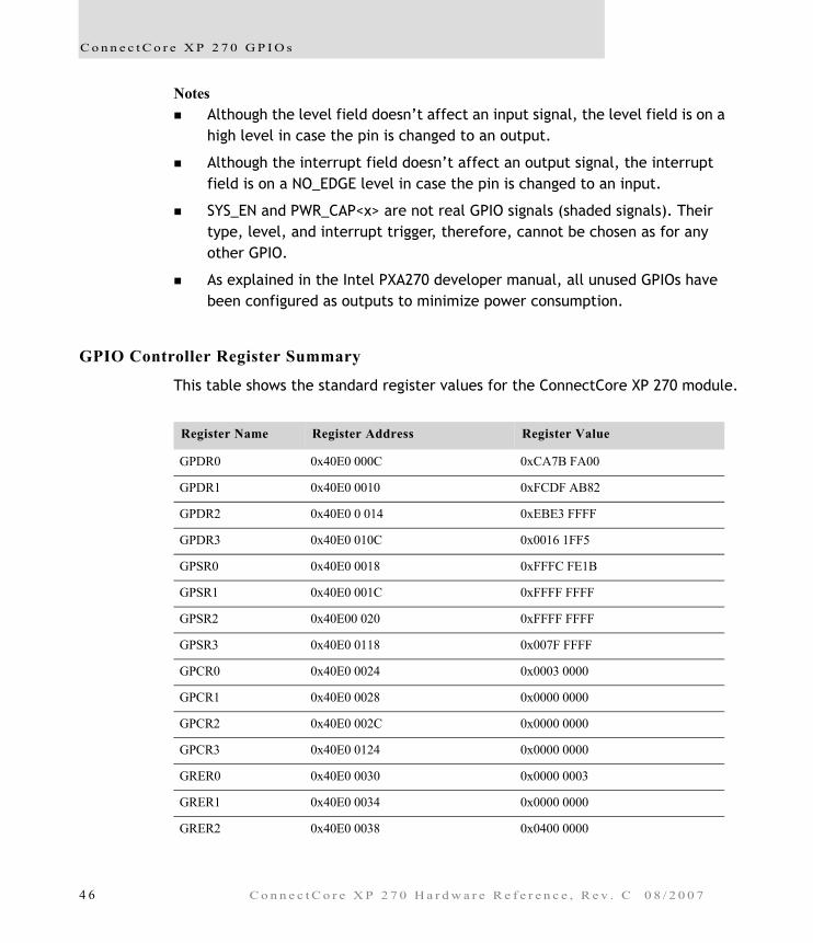
GPIO Controller Register Summary
This table shows the standard register values for the ConnectCore XP 270 module.
Register Name Register Address Register Value
GPDR0 0x40E0 000C 0xCA7B FA00
GPDR1 0x40E0 0010 0xFCDF AB82
GPDR2 0x40E0 0 014 0xEBE3 FFFF
GPDR3 0x40E0 010C 0x0016 1FF5
GPSR0 0x40E0 0018 0xFFFC FE1B
GPSR1 0x40E0 001C 0xFFFF FFFF
GPSR2 0x40E00 020 0xFFFF FFFF
GPSR3 0x40E0 0118 0x007F FFFF
GPCR0 0x40E0 0024 0x0003 0000
GPCR1 0x40E0 0028 0x0000 0000
GPCR2 0x40E0 002C 0x0000 0000
GPCR3 0x40E0 0124 0x0000 0000
GRER0 0x40E0 0030 0x0000 0003
GRER1 0x40E0 0034 0x0000 0000
GRER2 0x40E0 0038 0x0400 0000
4 6 C o n n e c t C o r e X P 2 7 0 H a r d w a r e R e f e r e n c e , R e v . C 0 8 / 2 0 0 7
A b o u t t h e M o d u l e
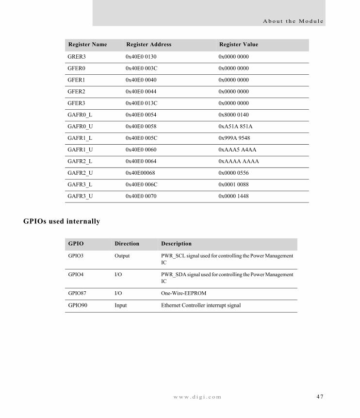
GPIOs used internally
GRER3 0x40E0 0130 0x0000 0000
GFER0 0x40E0 003C 0x0000 0000
GFER1 0x40E0 0040 0x0000 0000
GFER2 0x40E0 0044 0x0000 0000
GFER3 0x40E0 013C 0x0000 0000
GAFR0_L 0x40E0 0054 0x8000 0140
GAFR0_U 0x40E0 0058 0xA51A 851A
GAFR1_L 0x40E0 005C 0x999A 9548
GAFR1_U 0x40E0 0060 0xAAA5 A4AA
GAFR2_L 0x40E0 0064 0xAAAA AAAA
GAFR2_U 0x40E00068 0x0000 0556
GAFR3_L 0x40E0 006C 0x0001 0088
GAFR3_U 0x40E0 0070 0x0000 1448
Register Name Register Address Register Value
GPIO Direction Description
GPIO3 Output PWR_SCL signal used for controlling the Power Management IC
GPIO4 I/O PWR_SDA signal used for controlling the Power Management IC
GPIO87 I/O One-Wire-EEPROM
GPIO90 Input Ethernet Controller interrupt signal
w w w . d i g i . c o m 4 7
C o n n e c t C o r e X P 2 7 0 M e m o r y M a p
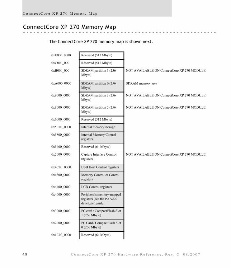
ConnectCore XP 270 Memory Map
The ConnectCore XP 270 memory map is shown next.
0xE000_0000 Reserved (512 Mbyte)
0xC000_000 Reserved (512 Mbyte)
0xB000_000 SDRAM partition 1 (256 Mbyte)
NOT AVAILABLE ON ConnectCore XP 270 MODULE
0xA000_0000 SDRAM partition 0 (256 Mbyte)
SDRAM memory area
0x9000_0000 SDRAM partition 3 (256 Mbyte)
NOT AVAILABLE ON ConnectCore XP 270 MODULE
0x8000_0000 SDRAM partition 2 (256 Mbyte)
NOT AVAILABLE ON ConnectCore XP 270 MODULE
0x6000_0000 Reserved (512 Mbyte)
0x5C00_0000 Internal memory storage
0x5800_0000 Internal Memory Control registers
0x5400_0000 Reserved (64 Mbyte)
0x5000_0000 Capture Interface Control registers
NOT AVAILABLE ON ConnectCore XP 270 MODULE
0x4C00_0000 USB Host Control registers
0x4800_0000 Memory Controller Control registers
0x4400_0000 LCD Control registers
0x4000_0000 Peripherals memory-mapped registers (see the PXA270 developer guide)
0x3000_0000 PC card / CompactFlash Slot 1 (256 Mbyte)
0x2000_0000 PC Card / CompactFlash Slot 0 (256 Mbyte)
0x1C00_0000 Reserved (64 Mbyte)
4 8 C o n n e c t C o r e X P 2 7 0 H a r d w a r e R e f e r e n c e , R e v . C 0 8 / 2 0 0 7
A b o u t t h e M o d u l e
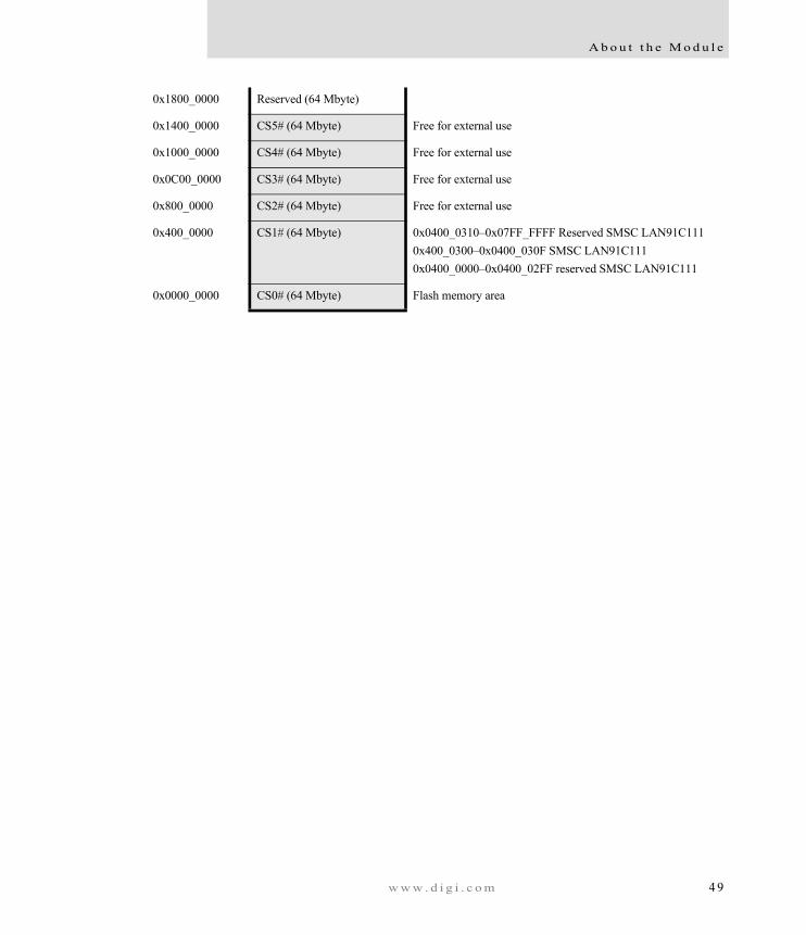
0x1800_0000 Reserved (64 Mbyte)
0x1400_0000 CS5# (64 Mbyte) Free for external use
0x1000_0000 CS4# (64 Mbyte) Free for external use
0x0C00_0000 CS3# (64 Mbyte) Free for external use
0x800_0000 CS2# (64 Mbyte) Free for external use
0x400_0000 CS1# (64 Mbyte) 0x0400_0310–0x07FF_FFFF Reserved SMSC LAN91C1110x400_0300–0x0400_030F SMSC LAN91C1110x0400_0000–0x0400_02FF reserved SMSC LAN91C111
0x0000_0000 CS0# (64 Mbyte) Flash memory area
w w w . d i g i . c o m 4 9

C o n n e c t C o r e X P 2 7 0 M e m o r y M a p
5 0 C o n n e c t C o r e X P 2 7 0 H a r d w a r e R e f e r e n c e , R e v . C 0 8 / 2 0 0 7

About the Development BoardC H A P T E R 2
This chapter provides information for configuring the ConnectCore XP 270 development board.
5 1
X S c a l e
XScale
Intel XScale is a 32-bit RISC microarchitecture based on architecture by Advanced RISC Machines (ARM), now the most popular 32-bit embedded CPU family in the world. ARM-based and Intel XScale technology are completely binary compatible, so software and software-developed tools designed for older ARM processors also work on newer Intel XScale core-based processors.
The Intel XScale RISC microarchitecture is noted for its efficiency. It obtains high performance, minimal number of silicon transistors, which require less power to operate the chip. It also means the chip processor itself will take up less silicon, making it smaller and less expensive to manufacture in volume. This combination of high performance, small size, low power, and modest cost gives the Intel PXA270 applications processor some compelling advantages over competing processors.
The Intel XScale core in the Intel PXA270 applications processor is a generational improvement over the previous Intel® StrongARM* processors, the Intel® SA-1100 and the Intel® SA-1110. Unlike the SA chips, the Intel PXA270 applications processor includes the ARM® Thumb® code-compression technology. The Thumb technology compresses software density by about 30 percent over normal RISC code. This compression (and the corresponding real-time decompression) is handled automatically by the Intel PXA270 applications processor; engineers and programmers are generally unaware of its operation. They only notice the improved memory utilization.
Another improvement in the Intel XScale core is the dual-multiply/accumulate (dual- MAC) instruction. A MAC operation is a relatively new addition to most computers and microprocessors, borrowed from the Digital Signal Processor (DSP) world. MAC operations are so vital to many audio, video, and wireless applications, that one or two MAC instructions can dramatically benefit a chip’s ability to run these multimedia applications.
The improved processor technology additionally supports a new Turbo Mode clocking technique. Turbo Mode allows the user to clock the processor core at a higher frequency during peak processing requirements. It allows a synchronous switch in frequencies without disrupting the Memory Controller, LCD Controller, or any peripheral.
5 2 C o n n e c t C o r e X P 2 7 0 H a r d w a r e R e f e r e n c e , R e v . C 0 8 / 2 0 0 7
A b o u t t h e D e v e l o p m e n t B o a r d
The Intel PXA270 processor uses a new Micro-Power-Management that results in less than 50% power consumption, compared to a StrongARM SA-1110 processor running on the same clock speed.
What’s on the development board?
The ConnectCore XP 270 development board integrates all components that are necessary to operate the ConnectCore XP 270 module.
These are development board features. A picture of the development board, with the locations of connectors, sockets, and other components, follows the feature list.
200-pin ConnectCore XP 270 socket
Compact Flash card socket, selectable true IDE or CF mode
RS232 interface and connector
JTAG interface
All pins of the ConnectCore XP 270 socket are connected flat cable headers
Predecoded chip select signals
Buffered address and data bus
USB Device connector
USB Host controller and connector
40-pin universal LCD flat cable header
Daughter board slot for easy application design-in
Ethernet magnetics and connector for ConnectCore XP 270 onboard Ethernet controllers
Disconnectable ConnectCore XP 270 power supply for power consumption measurements
3.3V single supply design; 5V also available onboard
Single power supply: 12VDC
w w w . d i g i . c o m 5 3
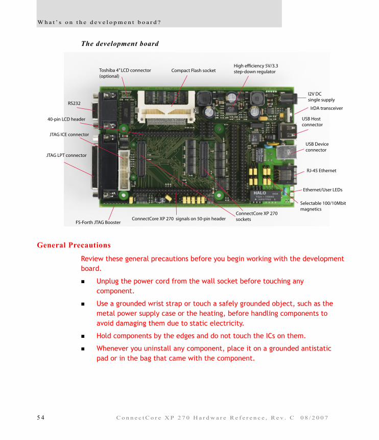
W h a t ’ s o n t h e d e v e l o p m e n t b o a r d ?
The development board
General Precautions
Review these general precautions before you begin working with the development board.
Unplug the power cord from the wall socket before touching any component.
Use a grounded wrist strap or touch a safely grounded object, such as the metal power supply case or the heating, before handling components to avoid damaging them due to static electricity.
Hold components by the edges and do not touch the ICs on them.
Whenever you uninstall any component, place it on a grounded antistatic pad or in the bag that came with the component.
5 4 C o n n e c t C o r e X P 2 7 0 H a r d w a r e R e f e r e n c e , R e v . C 0 8 / 2 0 0 7
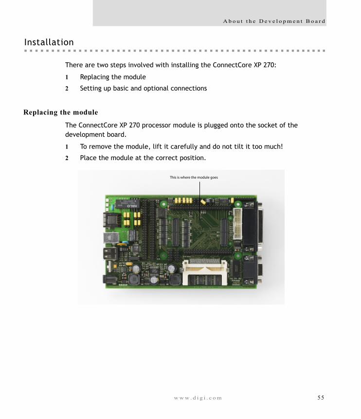
A b o u t t h e D e v e l o p m e n t B o a r d
Installation
There are two steps involved with installing the ConnectCore XP 270:
1 Replacing the module
2 Setting up basic and optional connections
Replacing the module
The ConnectCore XP 270 processor module is plugged onto the socket of the development board.
1 To remove the module, lift it carefully and do not tilt it too much!
2 Place the module at the correct position.
w w w . d i g i . c o m 5 5
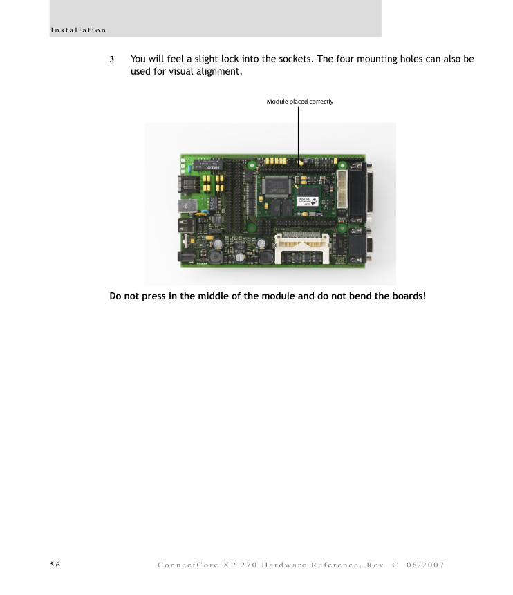
I n s t a l l a t i o n
3 You will feel a slight lock into the sockets. The four mounting holes can also be used for visual alignment.
Do not press in the middle of the module and do not bend the boards!
5 6 C o n n e c t C o r e X P 2 7 0 H a r d w a r e R e f e r e n c e , R e v . C 0 8 / 2 0 0 7
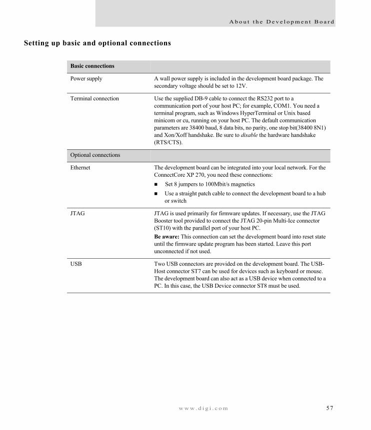
A b o u t t h e D e v e l o p m e n t B o a r d
Setting up basic and optional connections
Basic connections
Power supply A wall power supply is included in the development board package. The secondary voltage should be set to 12V.
Terminal connection Use the supplied DB-9 cable to connect the RS232 port to a communication port of your host PC; for example, COM1. You need a terminal program, such as Windows HyperTerminal or Unix based minicom or cu, running on your host PC. The default communication parameters are 38400 baud, 8 data bits, no parity, one stop bit(38400 8N1) and Xon/Xoff handshake. Be sure to disable the hardware handshake (RTS/CTS).
Optional connections
Ethernet The development board can be integrated into your local network. For the ConnectCore XP 270, you need these connections: Set 8 jumpers to 100Mbit/s magnetics Use a straight patch cable to connect the development board to a hub
or switch
JTAG JTAG is used primarily for firmware updates. If necessary, use the JTAG Booster tool provided to connect the JTAG 20-pin Multi-Ice connector (ST10) with the parallel port of your host PC. Be aware: This connection can set the development board into reset state until the firmware update program has been started. Leave this port unconnected if not used.
USB Two USB connectors are provided on the development board. The USB-Host connector ST7 can be used for devices such as keyboard or mouse. The development board can also act as a USB device when connected to a PC. In this case, the USB Device connector ST8 must be used.
w w w . d i g i . c o m 5 7
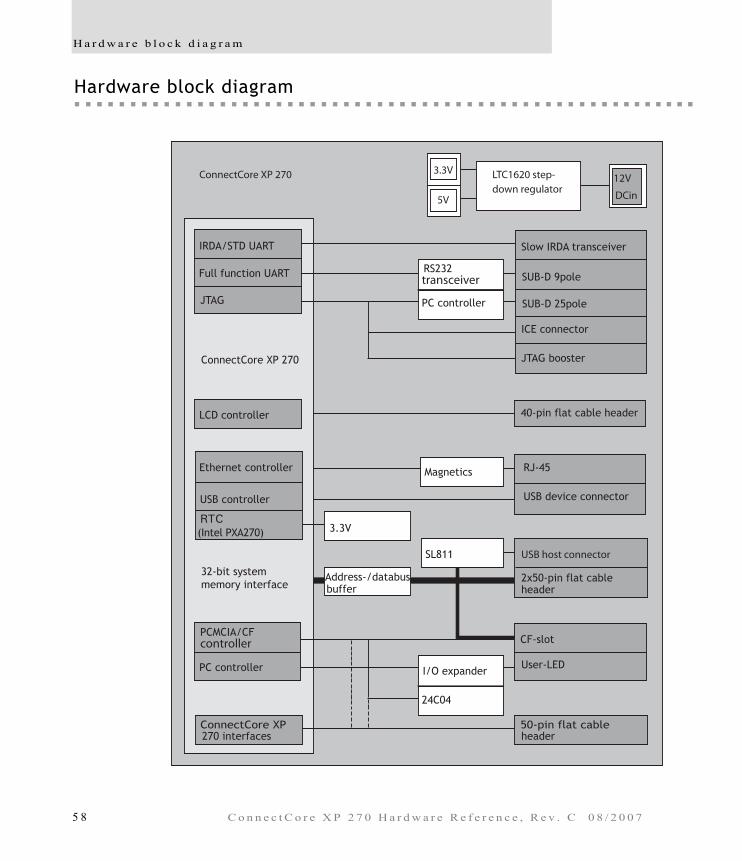
H a r d w a r e b l o c k d i a g r a m
Hardware block diagram
5 8 C o n n e c t C o r e X P 2 7 0 H a r d w a r e R e f e r e n c e , R e v . C 0 8 / 2 0 0 7
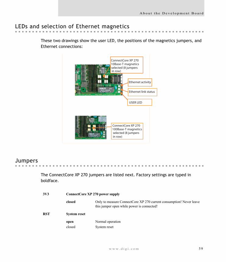
A b o u t t h e D e v e l o p m e n t B o a r d
LEDs and selection of Ethernet magnetics
These two drawings show the user LED, the positions of the magnetics jumpers, and Ethernet connections:
Jumpers
The ConnectCore XP 270 jumpers are listed next. Factory settings are typed in boldface.
3V3 ConnectCore XP 270 power supply
closed Only to measure ConnectCore XP 270 current consumption! Never leave this jumper open while power is connected!
RST System reset
openclosed
Normal operationSystem reset
w w w . d i g i . c o m 5 9
J u m p e r s
BVD2 Compact-Flash BVD2/SPKR/DASP (leave jumper LINKLED open if closed)
openclosed
GPIO33 (pin 114) free for useCompact-Flash BVD2 routed to GPIO33 (pin 114)
BVD1 Compact-Flash BVD1/STSCHG/PDIAG (leave jumper CD open if closed)
openclosed
GPIO80 (pin 115) free for useCompact-Flash BVD1 routed to GPIO80 (pin 115)
IDE Compact-Flash operation mode
openclosed
Compact-Flash modeTrue IDE mode
CFINT Compact-Flash interrupt
openclosed
GPIO10 (pin 53) free for useCompact-Flash interrupt routed to GPIO10 (pin 53)
CD Compact-Flash Card_Detect (leave jumper BVD1 open if closed)
openclosed
GPIO80 (pin 115) free for useCompact-Flash CD1 ored with CD2 routed to GPIO80 (pin 115)
LINKLED Ethernet Link LED (leave jumper BVD2 open if closed)
openclosed
GPIO33 (pin 114) free for useEthernet Link LED routed to GPIO33 (pin 114) to realize wake on LAN functionality
I2CINT I2C Controller interrupt
openclosed
GPIO11 (pin 54) free for useI2C Controller interrupt routed to GPIO11 (pin 54)
6 0 C o n n e c t C o r e X P 2 7 0 H a r d w a r e R e f e r e n c e , R e v . C 0 8 / 2 0 0 7
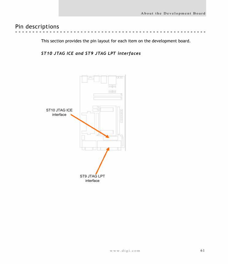
A b o u t t h e D e v e l o p m e n t B o a r d
Pin descriptions
This section provides the pin layout for each item on the development board.
ST10 JTAG ICE and ST9 JTAG LPT interfaces
ST10 JTAG ICEinterface
ST9 JTAG LPTinterface
w w w . d i g i . c o m 6 1
P i n d e s c r i p t i o n s
ST10 JTAG ICE interface pin assignments
1 3V3
2 3V3
3 #TRST
4 GND
5 TDI
6 GND
7 TMS
8 GND
9 TCK
10 GND
11 GND
12 GND
13 TDO
14 GND
15 #SRESET System reset
16 GND
17 not connected
18 GND
19 not connected
20 GND
6 2 C o n n e c t C o r e X P 2 7 0 H a r d w a r e R e f e r e n c e , R e v . C 0 8 / 2 0 0 7
A b o u t t h e D e v e l o p m e n t B o a r d
ST9 JTAG LPT interface pin assignments
1 not connected
2 TCK
3 TDI
4 TMS
5 #TRST
6 #ENAB Enable JTAG LPT interface
7 #SRESET System reset
8 not connected
9 not connected
10 not connected
11 TDO
12 not connected
13 connected
14 not connected
15 not connected
16 not connected
17 not connected
18 not connected
19 not connected
20 GND
21 GND
22 GND
23 GND
24 GND
25 GND
w w w . d i g i . c o m 6 3
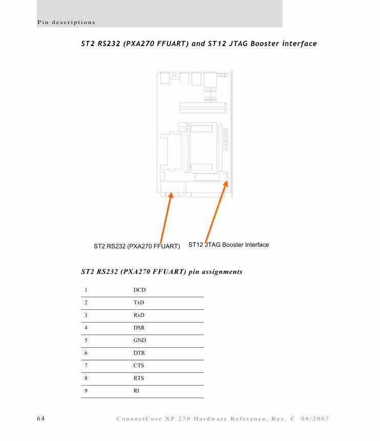
P i n d e s c r i p t i o n s
ST2 RS232 (PXA270 FFUART) and ST12 JTAG Booster interface
ST2 RS232 (PXA270 FFUART) pin assignments
1 DCD
2 TxD
3 RxD
4 DSR
5 GND
6 DTR
7 CTS
8 RTS
9 RI
ST2 RS232 (PXA270 FFUART) ST12 JTAG Booster Interface
6 4 C o n n e c t C o r e X P 2 7 0 H a r d w a r e R e f e r e n c e , R e v . C 0 8 / 2 0 0 7
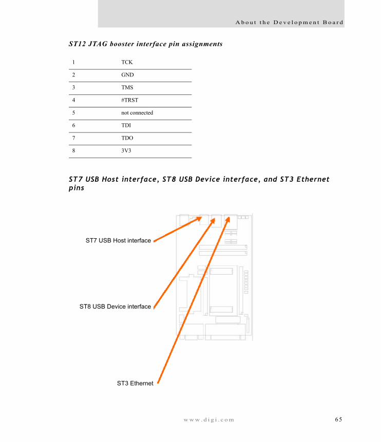
A b o u t t h e D e v e l o p m e n t B o a r d
ST12 JTAG booster interface pin assignments
ST7 USB Host interface, ST8 USB Device interface, and ST3 Ethernet pins
1 TCK
2 GND
3 TMS
4 #TRST
5 not connected
6 TDI
7 TDO
8 3V3
ST7 USB Host interface
ST8 USB Device interface
ST3 Ethernet
w w w . d i g i . c o m 6 5
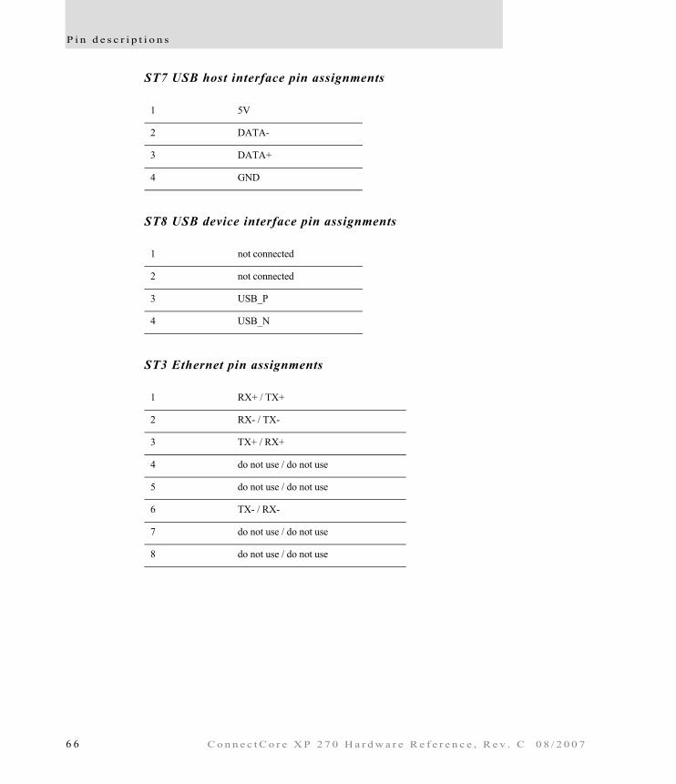
P i n d e s c r i p t i o n s
ST7 USB host interface pin assignments
ST8 USB device interface pin assignments
ST3 Ethernet pin assignments
1 5V
2 DATA-
3 DATA+
4 GND
1 not connected
2 not connected
3 USB_P
4 USB_N
1 RX+ / TX+
2 RX- / TX-
3 TX+ / RX+
4 do not use / do not use
5 do not use / do not use
6 TX- / RX-
7 do not use / do not use
8 do not use / do not use
6 6 C o n n e c t C o r e X P 2 7 0 H a r d w a r e R e f e r e n c e , R e v . C 0 8 / 2 0 0 7
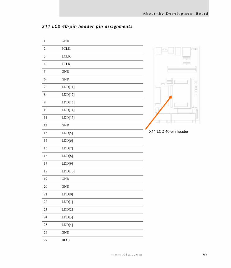
A b o u t t h e D e v e l o p m e n t B o a r d
X11 LCD 40-pin header pin assignments
1 GND
2 PCLK
3 LCLK
4 FCLK
5 GND
6 GND
7 LDD[11]
8 LDD[12]
9 LDD[13]
10 LDD[14]
11 LDD[15]
12 GND
13 LDD[5]
14 LDD[6]
15 LDD[7]
16 LDD[8]
17 LDD[9]
18 LDD[10]
19 GND
20 GND
21 LDD[0]
22 LDD[1]
23 LDD[2]
24 LDD[3]
25 LDD[4]
26 GND
27 BIAS
X11 LCD 40-pin header
w w w . d i g i . c o m 6 7

P i n d e s c r i p t i o n s
28 3V3
29 3V3
30 GPIO10
31 GPIO11
32 BLI_CON Backlight ON (PCF8574/P4)
33 5V
34 5V
35 GND
36 GND
37 TSMX Touchscreen X-
38 TSMY Touchscreen Y-
39 TSPX Touchscreen X+
40 TSPY Touchscreen Y+
6 8 C o n n e c t C o r e X P 2 7 0 H a r d w a r e R e f e r e n c e , R e v . C 0 8 / 2 0 0 7
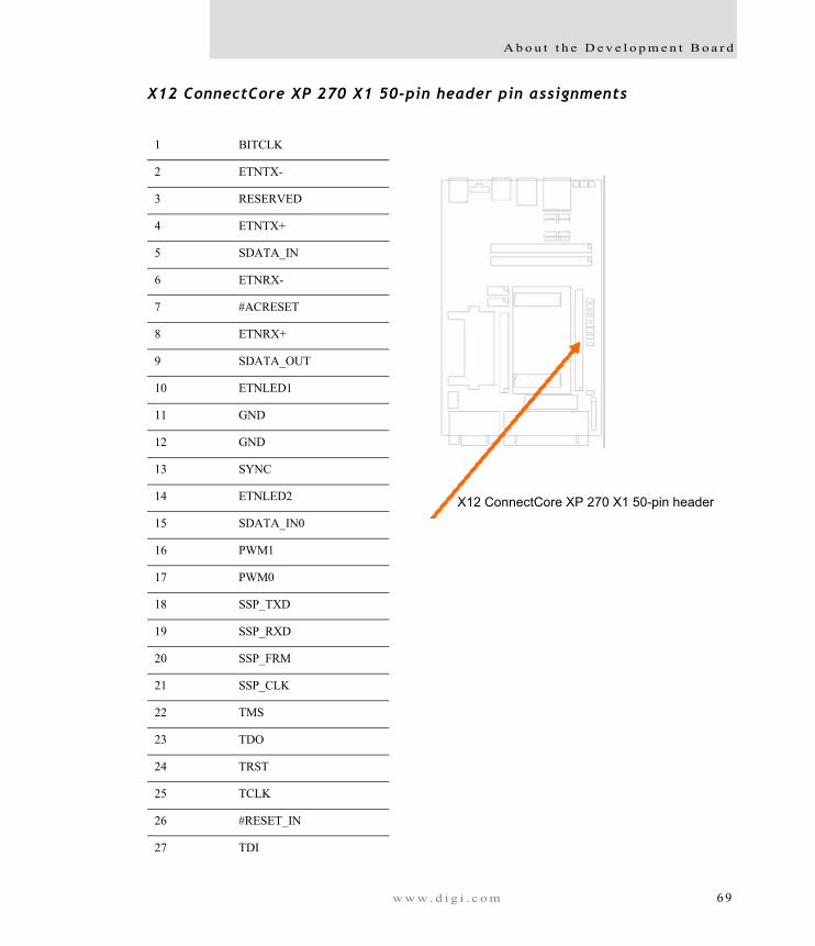
A b o u t t h e D e v e l o p m e n t B o a r d
X12 ConnectCore XP 270 X1 50-pin header pin assignments
1 BITCLK
2 ETNTX-
3 RESERVED
4 ETNTX+
5 SDATA_IN
6 ETNRX-
7 #ACRESET
8 ETNRX+
9 SDATA_OUT
10 ETNLED1
11 GND
12 GND
13 SYNC
14 ETNLED2
15 SDATA_IN0
16 PWM1
17 PWM0
18 SSP_TXD
19 SSP_RXD
20 SSP_FRM
21 SSP_CLK
22 TMS
23 TDO
24 TRST
25 TCLK
26 #RESET_IN
27 TDI
X12 ConnectCore XP 270 X1 50-pin header
w w w . d i g i . c o m 6 9
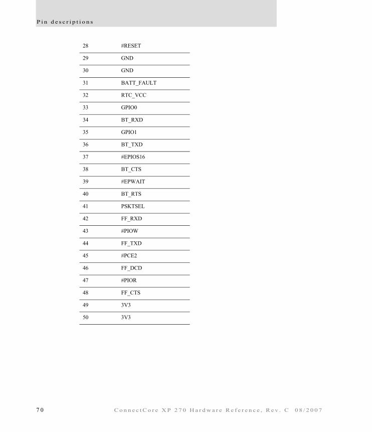
P i n d e s c r i p t i o n s
28 #RESET
29 GND
30 GND
31 BATT_FAULT
32 RTC_VCC
33 GPIO0
34 BT_RXD
35 GPIO1
36 BT_TXD
37 #EPIOS16
38 BT_CTS
39 #EPWAIT
40 BT_RTS
41 PSKTSEL
42 FF_RXD
43 #PIOW
44 FF_TXD
45 #PCE2
46 FF_DCD
47 #PIOR
48 FF_CTS
49 3V3
50 3V3
7 0 C o n n e c t C o r e X P 2 7 0 H a r d w a r e R e f e r e n c e , R e v . C 0 8 / 2 0 0 7
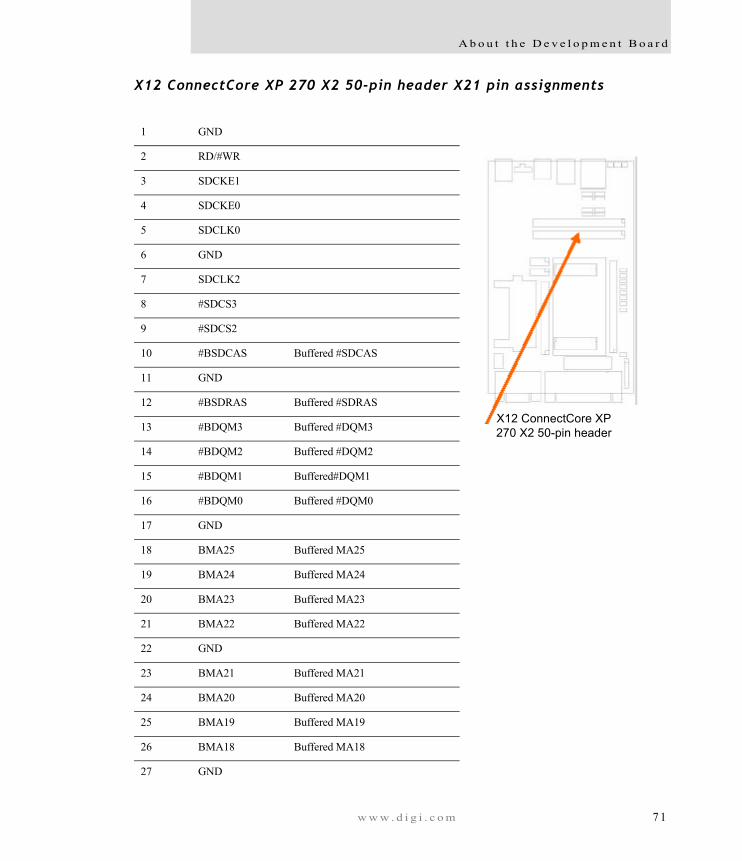
A b o u t t h e D e v e l o p m e n t B o a r d
X12 ConnectCore XP 270 X2 50-pin header X21 pin assignments
1 GND
2 RD/#WR
3 SDCKE1
4 SDCKE0
5 SDCLK0
6 GND
7 SDCLK2
8 #SDCS3
9 #SDCS2
10 #BSDCAS Buffered #SDCAS
11 GND
12 #BSDRAS Buffered #SDRAS
13 #BDQM3 Buffered #DQM3
14 #BDQM2 Buffered #DQM2
15 #BDQM1 Buffered#DQM1
16 #BDQM0 Buffered #DQM0
17 GND
18 BMA25 Buffered MA25
19 BMA24 Buffered MA24
20 BMA23 Buffered MA23
21 BMA22 Buffered MA22
22 GND
23 BMA21 Buffered MA21
24 BMA20 Buffered MA20
25 BMA19 Buffered MA19
26 BMA18 Buffered MA18
27 GND
X12 ConnectCore XP270 X2 50-pin header
w w w . d i g i . c o m 7 1
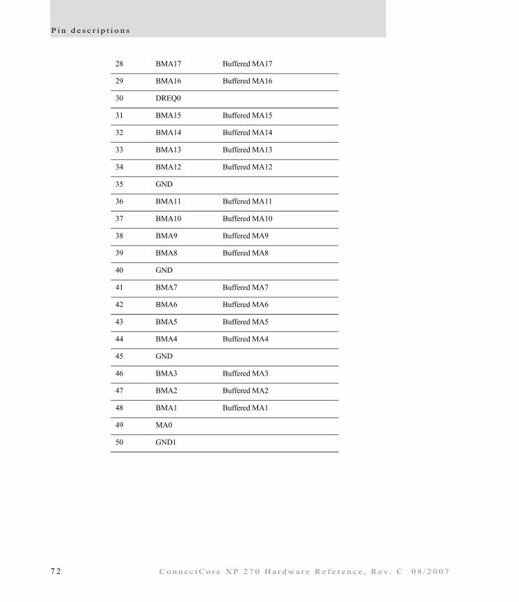
P i n d e s c r i p t i o n s
28 BMA17 Buffered MA17
29 BMA16 Buffered MA16
30 DREQ0
31 BMA15 Buffered MA15
32 BMA14 Buffered MA14
33 BMA13 Buffered MA13
34 BMA12 Buffered MA12
35 GND
36 BMA11 Buffered MA11
37 BMA10 Buffered MA10
38 BMA9 Buffered MA9
39 BMA8 Buffered MA8
40 GND
41 BMA7 Buffered MA7
42 BMA6 Buffered MA6
43 BMA5 Buffered MA5
44 BMA4 Buffered MA4
45 GND
46 BMA3 Buffered MA3
47 BMA2 Buffered MA2
48 BMA1 Buffered MA1
49 MA0
50 GND1
7 2 C o n n e c t C o r e X P 2 7 0 H a r d w a r e R e f e r e n c e , R e v . C 0 8 / 2 0 0 7
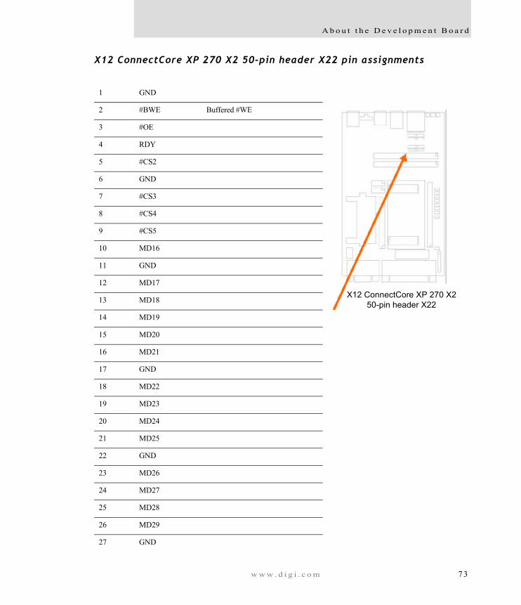
A b o u t t h e D e v e l o p m e n t B o a r d
X12 ConnectCore XP 270 X2 50-pin header X22 pin assignments
1 GND
2 #BWE Buffered #WE
3 #OE
4 RDY
5 #CS2
6 GND
7 #CS3
8 #CS4
9 #CS5
10 MD16
11 GND
12 MD17
13 MD18
14 MD19
15 MD20
16 MD21
17 GND
18 MD22
19 MD23
20 MD24
21 MD25
22 GND
23 MD26
24 MD27
25 MD28
26 MD29
27 GND
X12 ConnectCore XP 270 X250-pin header X22
w w w . d i g i . c o m 7 3
P i n d e s c r i p t i o n s
28 MD30
29 MD31
30 DREQ1
31 MD15
32 MD7
33 MD14
34 MD6
35 GND
36 MD13
37 MD5
38 MD12
39 MD4
40 GND
41 MD11
42 MD3
43 MD10
44 MD2
45 GND
46 MD9
47 MD1
48 MD8
49 MD0
50 GND
7 4 C o n n e c t C o r e X P 2 7 0 H a r d w a r e R e f e r e n c e , R e v . C 0 8 / 2 0 0 7
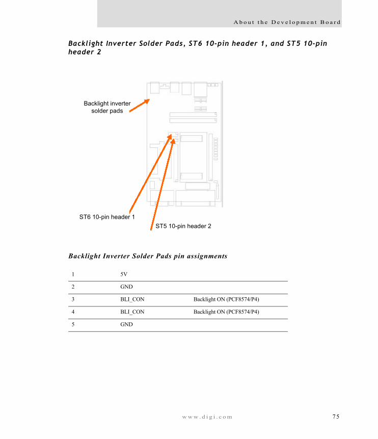
A b o u t t h e D e v e l o p m e n t B o a r d
Backlight Inverter Solder Pads, ST6 10-pin header 1, and ST5 10-pin header 2
Backlight Inverter Solder Pads pin assignments
1 5V
2 GND
3 BLI_CON Backlight ON (PCF8574/P4)
4 BLI_CON Backlight ON (PCF8574/P4)
5 GND
Backlight invertersolder pads
ST6 10-pin header 1ST5 10-pin header 2
w w w . d i g i . c o m 7 5
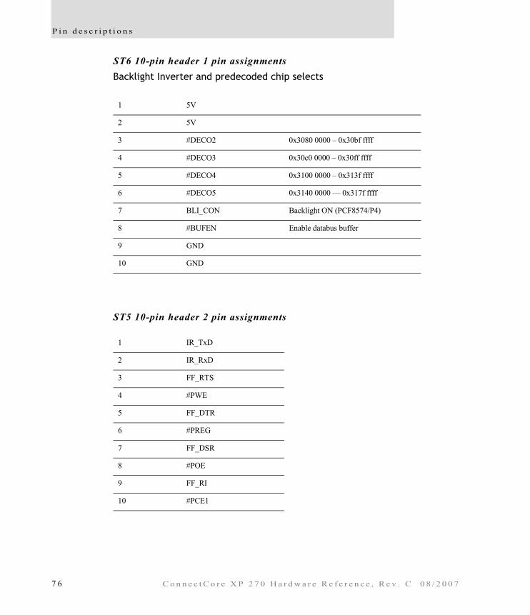
P i n d e s c r i p t i o n s
ST6 10-pin header 1 pin assignmentsBacklight Inverter and predecoded chip selects
ST5 10-pin header 2 pin assignments
1 5V
2 5V
3 #DECO2 0x3080 0000 – 0x30bf ffff
4 #DECO3 0x30c0 0000 – 0x30ff ffff
5 #DECO4 0x3100 0000 – 0x313f ffff
6 #DECO5 0x3140 0000 — 0x317f ffff
7 BLI_CON Backlight ON (PCF8574/P4)
8 #BUFEN Enable databus buffer
9 GND
10 GND
1 IR_TxD
2 IR_RxD
3 FF_RTS
4 #PWE
5 FF_DTR
6 #PREG
7 FF_DSR
8 #POE
9 FF_RI
10 #PCE1
7 6 C o n n e c t C o r e X P 2 7 0 H a r d w a r e R e f e r e n c e , R e v . C 0 8 / 2 0 0 7
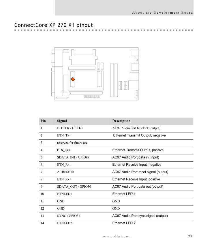
A b o u t t h e D e v e l o p m e n t B o a r d
ConnectCore XP 270 X1 pinout
Pin Signal Description
1 BITCLK / GPIO28 AC97 Audio Port bit clock (output)
2 ETN_Tx- Ethernet Transmit Output, negative
3 reserved for future use
4 ETN_Tx+ Ethernet Transmit Output, positive
5 SDATA_IN1 / GPIO99 AC97 Audio Port data in (input)
6 ETN_Rx- Ethernet Receive Input, negative
7 ACRESET# AC97 Audio Port reset signal (output)
8 ETN_Rx+ Ethernet Receive Input, positive
9 SDATA_OUT / GPIO30 AC97 Audio Port data out (output)
10 ETNLED1 Ethernet LED 1
11 GND GND
12 GND GND
13 SYNC / GPIO31 AC97 Audio Port sync signal (output)
14 ETNLED2 Ethernet LED 2
w w w . d i g i . c o m 7 7
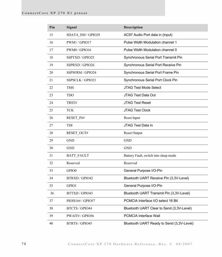
C o n n e c t C o r e X P 2 7 0 X 1 p i n o u t
15 SDATA_IN0 / GPIO29 AC97 Audio Port data in (input)
16 PWM1 / GPIO17 Pulse Width Modulation channel 1
17 PWM0 / GPIO16 Pulse Width Modulation channel 0
18 SSPTXD / GPIO25 Synchronous Serial Port Transmit Pin
19 SSPRXD / GPIO26 Synchronous Serial Port Receive Pin
20 SSPSFRM / GPIO24 Synchronous Serial Port Frame Pin
21 SSPSCLK / GPIO23 Synchronous Serial Port Clock Pin
22 TMS JTAG Test Mode Select
23 TDO JTAG Test Data Out
24 TRST# JTAG Test Reset
25 TCK JTAG Test Clock
26 RESET_IN# Reset Input
27 TDI JTAG Test Data In
28 RESET_OUT# Reset Output
29 GND GND
30 GND GND
31 BATT_FAULT Battery Fault, switch into sleep mode
32 Reserved Reserved
33 GPIO0 General Purpose I/O-Pin
34 BTRXD / GPIO42 Bluetooth UART Receive Pin (3,3V-Level)
35 GPIO1 General Purpose I/O-Pin
36 BTTXD / GPIO43 Bluetooth UART Transmit Pin (3,3V-Level)
37 PIOIS16# / GPIO57 PCMCIA Interface I/O select 16 Bit
38 BTCTS / GPIO44 Bluetooth UART Clear to Send (3,3V-Level)
39 PWAIT# / GPIO56 PCMCIA Interface Wait
40 BTRTS / GPIO45 Bluetooth UART Ready to Send (3,3V-Level)
Pin Signal Description
7 8 C o n n e c t C o r e X P 2 7 0 H a r d w a r e R e f e r e n c e , R e v . C 0 8 / 2 0 0 7
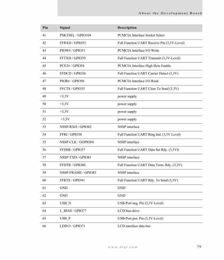
A b o u t t h e D e v e l o p m e n t B o a r d
41 PSKTSEL / GPIO104 PCMCIA Interface Socket Select
42 FFRXD / GPIO53 Full Function UART Receive Pin (3,3V-Level)
43 PIOW# / GPIO51 PCMCIA Interface I/O Write
44 FFTXD / GPIO39 Full Function UART Transmit (3,3V-Level)
45 PCE2# / GPIO54 PCMCIA Interface High Byte Enable
46 FFDCD / GPIO36 Full Function UART Carrier Detect (3,3V)
47 PIOR# / GPIO50 PCMCIA Interface I/O Read
48 FFCTS / GPIO35 Full Function UART Clear To Send (3,3V)
49 +3,3V power supply
50 +3,3V power supply
51 +3,3V power supply
52 +3,3V power supply
53 NSSP-RXD / GPIO82 NSSP interface
54 FFRI / GPIO38 Full Function UART Ring Ind. (3,3V Level)
55 NSSP-CLK / GOPIO84 NSSP interface
56 FFDSR / GPIO37 Full Function UART Data Set Rdy. (3,3Vl)
57 NSSP-TXD / GPIO81 NSSP interface
58 FFDTR / GPIO40 Full Function UART Data Term. Rdy. (3,3V)
59 NSSP-FRAME / GPIO83 NSSP interface
60 FFRTS / GPIO41 Full Function UART Rdy. To Send (3,3V)
61 GND GND
62 GND GND
63 USB_N USB-Port neg. Pin (3,3V-Level)
64 L_BIAS / GPIO77 LCD bias drive
65 USB_P USB-Port pos. Pin (3,3V-Level)
66 LDD13 / GPIO71 LCD interface data bus
Pin Signal Description
w w w . d i g i . c o m 7 9
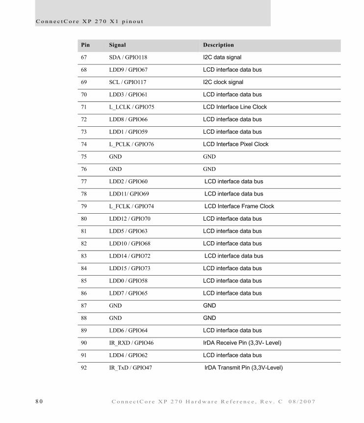
C o n n e c t C o r e X P 2 7 0 X 1 p i n o u t
67 SDA / GPIO118 I2C data signal
68 LDD9 / GPIO67 LCD interface data bus
69 SCL / GPIO117 I2C clock signal
70 LDD3 / GPIO61 LCD interface data bus
71 L_LCLK / GPIO75 LCD Interface Line Clock
72 LDD8 / GPIO66 LCD interface data bus
73 LDD1 / GPIO59 LCD interface data bus
74 L_PCLK / GPIO76 LCD Interface Pixel Clock
75 GND GND
76 GND GND
77 LDD2 / GPIO60 LCD interface data bus
78 LDD11/ GPIO69 LCD interface data bus
79 L_FCLK / GPIO74 LCD Interface Frame Clock
80 LDD12 / GPIO70 LCD interface data bus
81 LDD5 / GPIO63 LCD interface data bus
82 LDD10 / GPIO68 LCD interface data bus
83 LDD14 / GPIO72 LCD interface data bus
84 LDD15 / GPIO73 LCD interface data bus
85 LDD0 / GPIO58 LCD interface data bus
86 LDD7 / GPIO65 LCD interface data bus
87 GND GND
88 GND GND
89 LDD6 / GPIO64 LCD interface data bus
90 IR_RXD / GPIO46 IrDA Receive Pin (3,3V- Level)
91 LDD4 / GPIO62 LCD interface data bus
92 IR_TxD / GPIO47 IrDA Transmit Pin (3,3V-Level)
Pin Signal Description
8 0 C o n n e c t C o r e X P 2 7 0 H a r d w a r e R e f e r e n c e , R e v . C 0 8 / 2 0 0 7

A b o u t t h e D e v e l o p m e n t B o a r d
ConnectCore XP 270 X2 pinout
93 PCE1# / GPIO85 PCMCIA Interface Low Byte Enable
94 GPIO34 General Purpose I/O-Pin
95 POE# / GPIO48 PCMCIA Interface Output Enable
96 GPIO10 General Purpose I/O-Pin
97 PREG# / GPIO55 PCMCIA Interface Register Select
98 PWE# / GPIO49 PCMCIA Interface Write Enable
99 GND GND
100 GND GND
Pin Signal Description
Pin Signal Description
1 GND GND
2 GND GND
3 RD/WR# Read not Write
w w w . d i g i . c o m 8 1
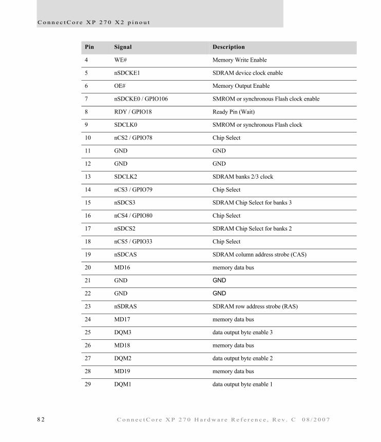
C o n n e c t C o r e X P 2 7 0 X 2 p i n o u t
4 WE# Memory Write Enable
5 nSDCKE1 SDRAM device clock enable
6 OE# Memory Output Enable
7 nSDCKE0 / GPIO106 SMROM or synchronous Flash clock enable
8 RDY / GPIO18 Ready Pin (Wait)
9 SDCLK0 SMROM or synchronous Flash clock
10 nCS2 / GPIO78 Chip Select
11 GND GND
12 GND GND
13 SDCLK2 SDRAM banks 2/3 clock
14 nCS3 / GPIO79 Chip Select
15 nSDCS3 SDRAM Chip Select for banks 3
16 nCS4 / GPIO80 Chip Select
17 nSDCS2 SDRAM Chip Select for banks 2
18 nCS5 / GPIO33 Chip Select
19 nSDCAS SDRAM column address strobe (CAS)
20 MD16 memory data bus
21 GND GND
22 GND GND
23 nSDRAS SDRAM row address strobe (RAS)
24 MD17 memory data bus
25 DQM3 data output byte enable 3
26 MD18 memory data bus
27 DQM2 data output byte enable 2
28 MD19 memory data bus
29 DQM1 data output byte enable 1
Pin Signal Description
8 2 C o n n e c t C o r e X P 2 7 0 H a r d w a r e R e f e r e n c e , R e v . C 0 8 / 2 0 0 7
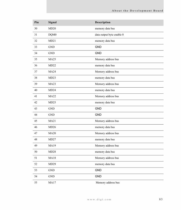
A b o u t t h e D e v e l o p m e n t B o a r d
30 MD20 memory data bus
31 DQM0 data output byte enable 0
32 MD21 memory data bus
33 GND GND
34 GND GND
35 MA25 Memory address bus
36 MD22 memory data bus
37 MA24 Memory address bus
38 MD23 memory data bus
39 MA23 Memory address bus
40 MD24 memory data bus
41 MA22 Memory address bus
42 MD25 memory data bus
43 GND GND
44 GND GND
45 MA21 Memory address bus
46 MD26 memory data bus
47 MA20 Memory address bus
48 MD27 memory data bus
49 MA19 Memory address bus
50 MD28 memory data bus
51 MA18 Memory address bus
52 MD29 memory data bus
53 GND GND
54 GND GND
55 MA17 Memory address bus
Pin Signal Description
w w w . d i g i . c o m 8 3
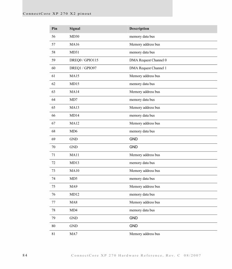
C o n n e c t C o r e X P 2 7 0 X 2 p i n o u t
56 MD30 memory data bus
57 MA16 Memory address bus
58 MD31 memory data bus
59 DREQ0 / GPIO115 DMA Request Channel 0
60 DREQ1 / GPIO97 DMA Request Channel 1
61 MA15 Memory address bus
62 MD15 memory data bus
63 MA14 Memory address bus
64 MD7 memory data bus
65 MA13 Memory address bus
66 MD14 memory data bus
67 MA12 Memory address bus
68 MD6 memory data bus
69 GND GND
70 GND GND
71 MA11 Memory address bus
72 MD13 memory data bus
73 MA10 Memory address bus
74 MD5 memory data bus
75 MA9 Memory address bus
76 MD12 memory data bus
77 MA8 Memory address bus
78 MD4 memory data bus
79 GND GND
80 GND GND
81 MA7 Memory address bus
Pin Signal Description
8 4 C o n n e c t C o r e X P 2 7 0 H a r d w a r e R e f e r e n c e , R e v . C 0 8 / 2 0 0 7
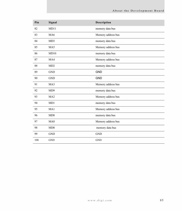
A b o u t t h e D e v e l o p m e n t B o a r d
82 MD11 memory data bus
83 MA6 Memory address bus
84 MD3 memory data bus
85 MA5 Memory address bus
86 MD10 memory data bus
87 MA4 Memory address bus
88 MD2 memory data bus
89 GND GND
90 GND GND
91 MA3 Memory address bus
92 MD9 memory data bus
93 MA2 Memory address bus
94 MD1 memory data bus
95 MA1 Memory address bus
96 MD8 memory data bus
97 MA0 Memory address bus
98 MD0 memory data bus
99 GND GND
100 GND GND
Pin Signal Description
w w w . d i g i . c o m 8 5

ConnectCore XP 270 CustomizationC H A P T E R 3
This chapter provides information for adding custom hardware to the ConnectCore XP 270 development board.
8 7
A d d i n g c u s t o m h a r d w a r e t o t h e d e v e l o p m e n t b o a r d
Adding custom hardware to the development board
You can use existing predecoded address areas to connect custom hardware to the ConnectCore XP 270 development board. These decoded address areas are in the PCMCIA socket 1 I/O space.
The development board has buffers for the address and data lines. The ConnectCore XP 270 module signals are connected to flat cable headers. The address and data lines are connected to the headers and routed from the buffers; they are not connected directly to ConnectCore XP 270 pins. These lines, as well as additional signals, are marked as buffered on the connector pinout (see "X12 ConnectCore XP 270 X2 50-pin header X21 pin assignments" on page 71).
The lower 16-bit databus buffers are automatically enabled for any access to the PCMCIA bus. If custom hardware is connected to one of the free static memory chip select signals, external hardware must enable the buffers. To enable the databus buffers during accesses to custom hardware, the active low #BUFEN signal must be used. For example, #BUFEN can be connected to the static chip select signal used if that’s the only signal used by custom hardware.
Chip selects CS[5:2] should have external 10K pullup resistors if used by custom hardware.
Custom development board design check list
This list provides hints and checkpoints for designing the development board. Use this list to ensure that you are designing the development board correctly and safely.
1 If you use one of the static chip selects CS2# - CS5#, do you have a pull up resistor on this line? The ConnectCore XP 270 module is provided with a 10K pullup on CS#[5..0]. Only CS#[5..2] are available externally on the module connectors.
2 The TRST# signal has a weak pull up on the development board. Intel recommends adding a 1.5 k pull-down resistor to TCK, on the development board.
8 8 C o n n e c t C o r e X P 2 7 0 H a r d w a r e R e f e r e n c e , R e v . C 0 8 / 2 0 0 7
C o n n e c t C o r e X P 2 7 0 C u s t o m i z a t i o n
3 If you use the onboard Ethernet controller, check the external magnetics circuitry carefully. The magnetics can be connected to the ConnectCore XP 270 module directly without additional components.
4 Check that you have at least one pullup resistor on the RESET_IN# signal (X1/26.)
5 Do you have buffers for the address bus and databus?
Note: There are no buffers on the ConnectCore XP 270 module itself. Use the shortest possible connection for these signals.
6 The maximum component height on the baseboard beneath the ConnectCore XP 270 module is 1.1mm.
7 nBATT_FAULT on connector X1 pin 31 is active low — leave open or tie to VCC if unused!
8 ConnectCore XP 270 signals are not 5V tolerant. Use buffers or level shifters for 5V signal interfacing.
w w w . d i g i . c o m 8 9

ConnectCore XP 270 Module SpecificationsA P P E N D I X A
This appendix provides specifics about the ConnectCore XP 270 module.
9 1
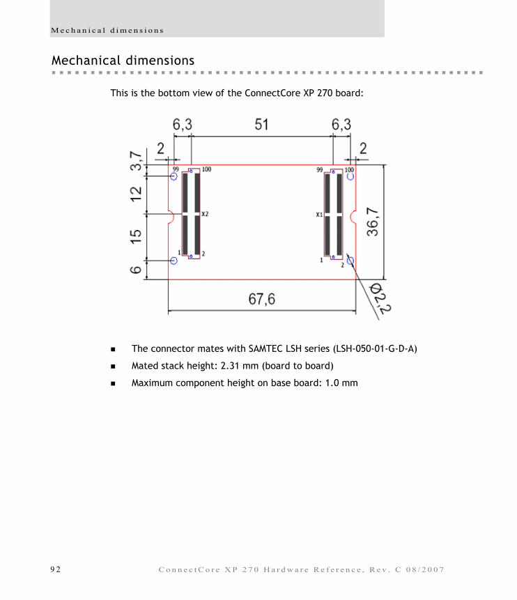
M e c h a n i c a l d i m e n s i o n s
Mechanical dimensions
This is the bottom view of the ConnectCore XP 270 board:
The connector mates with SAMTEC LSH series (LSH-050-01-G-D-A)
Mated stack height: 2.31 mm (board to board)
Maximum component height on base board: 1.0 mm
9 2 C o n n e c t C o r e X P 2 7 0 H a r d w a r e R e f e r e n c e , R e v . C 0 8 / 2 0 0 7
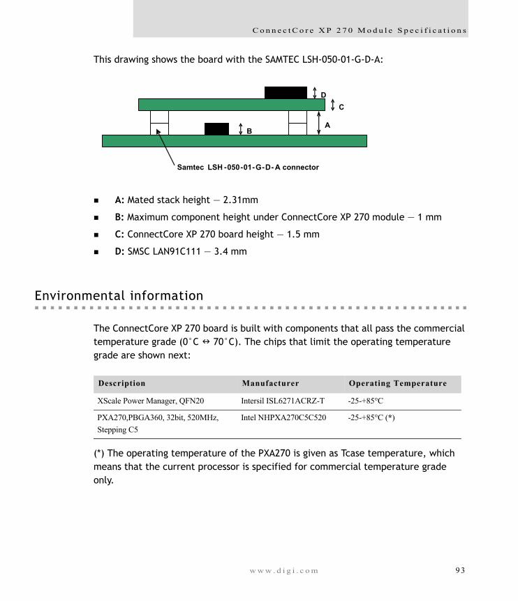
C o n n e c t C o r e X P 2 7 0 M o d u l e S p e c i f i c a t i o n s
This drawing shows the board with the SAMTEC LSH-050-01-G-D-A:
A: Mated stack height — 2.31mm
B: Maximum component height under ConnectCore XP 270 module — 1 mm
C: ConnectCore XP 270 board height — 1.5 mm
D: SMSC LAN91C111 — 3.4 mm
Environmental information
The ConnectCore XP 270 board is built with components that all pass the commercial temperature grade (0°C 70°C). The chips that limit the operating temperature grade are shown next:
(*) The operating temperature of the PXA270 is given as Tcase temperature, which means that the current processor is specified for commercial temperature grade only.
BA
CD
Samtec LSH -050-01-G-D- A connector
Description Manufacturer Operating Temperature
XScale Power Manager, QFN20 Intersil ISL6271ACRZ-T -25-+85°C
PXA270,PBGA360, 32bit, 520MHz, Stepping C5
Intel NHPXA270C5C520 -25-+85°C (*)
w w w . d i g i . c o m 9 3
P o w e r r e q u i r e m e n t s
Power requirements
The ConnectCore XP 270 module can impact management; for example, dynamically changing the core voltage. Clock frequency can also affect the current and case temperature of the PXA270 processor, as shown:
Layout considerations
When integrating the ConnectCore XP 270, special care must be taken with the Samtec LSH mating connectors. There is a keep out area for the layout, defined since Rev. 3 of Samtec’s LSH — Surface Mount Footprint definition. Note the connector’s profile shown next; there are two lead areas at the same level:
The outer area is used for soldering.
The inner area gives mechanical stability.
Note: In the case of copper on the PCB in the inner area, the soldermask is the only isolator and there is risk of a short circuit.
Clock frequency
Current needed
Power Tcase of PXA270
Comments
520 MHz 0.14 A 1680 mW 42.4 °C All measures have been made with room temperature at 30°C. Temperature measures have been made with Fluke 189 Multimeter and its temperature sensor.
9 4 C o n n e c t C o r e X P 2 7 0 H a r d w a r e R e f e r e n c e , R e v . C 0 8 / 2 0 0 7

C o n n e c t C o r e X P 2 7 0 M o d u l e S p e c i f i c a t i o n s
If all trace need to be routed inside the connector’s footprint, it must be ensured that only copper of the same net exists under each lead. If small vias are used, the fanout for all pads can be made completely inside the part outline. This example shows the LSH footprint and the two lead areas in red.
w w w . d i g i . c o m 9 5

JTAG-Booster for Intel XScale PXA270A P P E N D I X B
This appendix describes the JTAG booster as it is used with the Intel XScale PXA270 and the ConnectCore XP 270 module; in particular, using this tool to program flash memory.
9 7
O v e r v i e w
Overview
The program JTAG270.EXE uses the JTAG port of the Intel XScale PXA270 processor in conjunction with the small JTAG-Booster to perform these functions:
Program data into flash memory
Verify and read the contents of a flash memory
Make a memory dump
Access an I²C Device
Test CPU signals
All functions are done without any piece of software running in the target. No firmware or BIOS must be written. Bootstrap software may be downloaded to initially unprogrammed memories.
The JTAG-BOOSTER' s software is highly optimized to the JTAG chain of a specific target CPU.
Boundary Scan mode is extremely robust and may work on totally new and untested hardware. When you are bringing up new hardware or you are using this tool for the first time, you should start by using this standard mode.
OnChip Debug (OCD) mode allows higher download speed, but is more complex and relies on already working hardware.
System requirements
These are the system requirements for running this tool successfully:
MSDOS, WIN3.x, WIN9x, WinNT, Win2000 or WindowsXP (You need an additional tool to support WinNT/Win2000/WindowsXP; "Support for Windows NT, Windows 2000 and Windows XP," beginning on page 107.)
Intel 80386 or higher
205 kByte of free DOS memory
Parallel Port
9 8 n n n n n n n C o n n e c t C o r e X P 2 7 0 H a r d w a r e R e f e r e n c e , R e v . C 0 8 / 2 0 0 7

J T A G - B o o s t e r f o r I n t e l X S c a l e P X A 2 7 0
CD files
These files can be found on the CD in the JTAG directory.
JTAG270.EXE
JTAG270.OVL
jtag270.ini
jtag270.cfg
proguboot.bat
winnt21.zip
Connecting your PC to the target system
The JTAG-Booster can be plugged into standard parallel ports (LPT1-3) with a
DB25-Connector.
w w w . d i g i . c o m n n n n n n n 9 9
I n i t i a l i z a t i o n f i l e J T A G 2 7 0 . I N I
The 3.3V version of the JTAG-Booster (FS part number 285) is delivered together with this package. Don’t use the 5V version of the JTAG-Booster (FS part number 227) with a 3.3V target. Don’t apply 5V to the 3.3V version of the JTAG-Booster
Your target must be able to power the JTAG-Booster; it draws about 100mA.
Before you start the program, the JTAG-BOOSTER must be plugged to a parallel interface of your PC and to the target.
The utility is started with the general command line format: JTAG270JTAG270 /function [filename] [/option_1] ... [/option_n]
Note that the function must be the first argument, followed (if needed) by the filename.
If you want to cancel execution of JTAGxxx, press CTRL-Break-Key.
With any error, the program aborts with an MSDOS error level of one.
Initialization file JTAG270.INI
The initialization file defines the default direction and level of all CPU signals. This file must be carefully adapted to your design with the Intel XScale. The Target-Entry identifies your design, which is displayed with most commands.
When the program JTAG270.EXE is started, it scans the current directory for an existing initialization file named JTAG270.INI. If no entry is found, the default values are used. You can also specify the initialization file with the option /INI=. If the specified file isn't found, the program aborts with an error message.
The CPU pins can also be used with the functions /BLINK, /PIN? and /SAMPLE to test the signals on your design.
Add remarks using //.
Supported Flash devices
Type JTAG270 /LIST [optionlist] to get an online list of all flash types that can be used with the /DEVICE= option.
1 0 0 n n n n n n n C o n n e c t C o r e X P 2 7 0 H a r d w a r e R e f e r e n c e , R e v . C 0 8 / 2 0 0 7
J T A G - B o o s t e r f o r I n t e l X S c a l e P X A 2 7 0
JTAG270 Parameter Description
When you start JTAG270.EXE without any parameters, a help screen appears with all possible functions and options:
JTAG270 --- JTAG utility for Intel PXA27xCopyright (C) FS FORTH-SYSTEME GmbH, BreisachVersion 4.xx of xx/xx/xxxx
Programming of Flash-EPROMs and hardware tests on targets with theIntel PXA27x.The JTAG-Booster is needed to connect the parallel port of the PCto the JTAG port of the Intel PXA27x.
Usage: JTAG270 /function [filename] [/option_1] ... [/option_n]Supported functions: /P : Program a Flash Device /R : Read a Flash Device to file /V : Verify a Flash Device with file /DUMP : Make a target dump /PSER : Program a I2C/SPI/MicroWire Device with file /RSER : Read a I2C/SPI/MicroWire Device to file /VSER : Verify a I2C/SPI/MicroWire Device with file /DUMPSER: Make a dump of a I2C/SPI/MicroWire device /BLINK : Toggle a CPU pin /PIN? : Test a CPU pin /SAMPLE : Test a CPU pin while CPU is running /SNAP : Test all CPU pins while CPU is running /LIST : Print a list of supported Flash devices
Supported Options:
/CS0 /CS1 /CS2 /CS3 /CS4/CS5 /FAST /FAST= /OCD /NOCS/NOWRSETUP /NORAM /RESET /RESUME /TOP/BYTE-MODE /BM /CFI /CFIDEBUG /PAUSE/P /NODUMP /NOERASE /ERASEALL /NOWRBUFF/LATTICE /WIGGLER /PLS /TRITON1 /TRITON2/TRITON3 /LPT1 /LPT2 /LPT3 /LPT-BASE=/32BIT /16BIT /8BIT /NOMAN /LENGTH=/L= /FILE-OFFSET= /FO= /OFFSET= /O=/DELAY= /DEVICE-BASE= /DB= /DRIVER= /IROFFS=/CPUPOS= /DEVICE= /PIN= /SERCS= /SERCLK=/SERDAT= /SERDATI= /SERDATO= /SERBUFF= /SERBIG/SPI /MWIRE /DFLASH /LSB1ST /SPIERA/WATCH= /OUT= /INI= /CFG= /SCR=/REP
w w w . d i g i . c o m n n n n n n n 1 0 1
J T A G 2 7 0 P a r a m e t e r D e s c r i p t i o n
These options are the most important parameters for using JTAG270 software:
/DRIVER=x with x = 1,2,3,4You can specify a driver for the interface to the JTAG-BOOSTER on the parallel port. /DRIVER=1 selects the fastest available driver; /DRIVER=4 selects the slowest one. Use a slower driver if there are problems with JTAG-BOOSTER.
Default: /DRIVER=1
/INI=fileYou can specify an initialization file. By default, the current directory is searched for the file JTAG270.INI. If this file is not found and no initialization file is specified in the command line, default initialization values are used.
Note: The initialization file is not loaded for the functions /SAMPLE and /SNAP.
Default: /INI=JTAG270.INI
/LATTICEAlong with the standard JTAG-Booster interface, several simple “Parallel-Port-JTAG” interfaces are supported. With these interfaces, though. programming performance is reduced.
/LPT1 /LPT2 /LPT3You can specify a printer port where the JTAG-Booster resides. If you are using this program with WinNT, Win2000, or WinXP, you must specify /LPT2 or /LPT-BASE=378 to get access to the standard printer port.
/LPT-BASEYou can specify the physical I/O address of the printer port instead of the logical printer name. This option is useful if you work with WinNT, Win2000 or Windows XP, because the standard printer port is mapped as LPT2 here.
Use the option /LPT-BASE=378 to get a command line that works independent of the operation system.
1 0 2 n n n n n n n C o n n e c t C o r e X P 2 7 0 H a r d w a r e R e f e r e n c e , R e v . C 0 8 / 2 0 0 7
J T A G - B o o s t e r f o r I n t e l X S c a l e P X A 2 7 0
Program a Flash Device
Use: JTAG270 /P filename [optionlist]
The specified file is programmed into the flash memory. The flash status is polled after each cell is programmed (cell = 8-, 16- or 32-bit, depending on current data bus width). In the case of a programming error, the contents of the flash memory are written to a file with the extension DMP.
For a complete verify after programming, use an additional command line with the verify function. In most cases, this additional verify step is not needed.
Software normally detects the type of the flash device. When auto-detection fails, you should use the /DEVICE= option together with /8BIT or /16BIT or /32BIT to set the right flash device and configuration.
Options
/DEVICE=devicename
The flash device is detected automatically by switching to auto-select mode. In case of trouble, select the flash device using this parameter to avoid auto-detection. Combine this option with one of the following options that specify the data bus width and the option /BYTE-MODE, if applicable.
/8BIT /16BIT /32BITSpecifies the data bus width to the target flash device. You can speed up auto-detection if you specify the correct data bus size. You need this option together with the /DEVICE= option to explicitly specify a particular flash configuration.
/BYTE-MODEIf there is a flash device connected to the CPU, which has a byte mode pin (8 bit and 16/32 bit bus mode), you can force it to be used as 8 bit mode with the option/BYTE-MODE. In most cases, this option will not be needed.
/CFI
To be prepared for future flash chips, the JTAG-Booster integrates support for flashes that contain the CFI (Common Flash Interface) information structure. CFI support is
w w w . d i g i . c o m n n n n n n n 1 0 3

P r o g r a m a F l a s h D e v i c e
activated by adding the option /CFI to the command line. The JTAG-Booster then automatically searches in all available bus widths for all possible flash types and configurations instead of searching for the JEDEC identification code.
In case of an error, add the command line option /CFIDEBUG and redirect the program output into a file. Sending Digi this file helps in solving problems.
/NOMAN
If you use a flash device that is identical to one of the supported parts but is from a different manufacturer, use this option to suppress the comparison of the manufacturer identification code. It is recommended that you use this option with the /DEVICE= option to avoid failures in auto-detection.
/DEVICE-BASE=hhhhhh
Use this option to specify a flash device starting address. In most cases, where the flash device is selected with one of the CPU’s chip select pins, this parameter is not needed. If there is any decoding logic in your hardware, however, this option is necessary. This option is especially useful when there are several flash banks connected to one chip select and a sub decoding logic generates chip selects for these flash banks; this option can select a specific flash bank.
Default: /DEVICE-BASE=0
Abbreviation: /DB=
/OFFSET=hhhhhh
The programming starts at an offset of hhhhhh relative to the start address of the flash device. If the offset is negative, the offset specifies an address relative to the end of the flash device. See "/TOP" on page 104 for more information.
Default: /OFFSET=0
Abbreviation: /O=
/TOP
If the /TOP option is used, the /OFFSET= option specifies the address where the programming ends (plus one) instead of the starting address. This option is very
1 0 4 n n n n n n n C o n n e c t C o r e X P 2 7 0 H a r d w a r e R e f e r e n c e , R e v . C 0 8 / 2 0 0 7
J T A G - B o o s t e r f o r I n t e l X S c a l e P X A 2 7 0
important for Intel CPU architectures, because target execution always starts at the top of the address space.
/FILE-OFFSET=hhhhhh
If FILE-OFFSET is specified, the first hhhhhh bytes of the file are skipped and not programmed to target.
Default: /FILE-OFFSET=0
Abbreviation: /FO=
/LENGTH=hhhhhh
The number of programmed bytes can be limited to LENGTH. If no LENGTH is specified, the whole file is programmed.
Default: /LENGTH=4000000 (64 MByte)
Abbreviation: /L=
/NODUMP
In case of a verify error, the contents of the flash memory is written to a file with the extension .DMP. With /NODUMP, you can suppress this feature.
/ERASEALL
/ERASEALL erases the whole flash device. If this option isn't set, only those blocks are erased where new data should be written.
/NOERASE
/NOERASE prevents the flash device from being erased.
/CS0 /CS1 /CS2 /CS3 /CS4 /CS5
This options specifies one or more chip select signals to the flash memory. The used chip selects must be defined as output and inactive in the initialization file.
w w w . d i g i . c o m n n n n n n n 1 0 5

E x a m p l e w i t h I n t e l P X A 2 7 0
Example with Intel PXA270
In this simple example, it is assumed that the JTAG-Booster is connected to LPT1 of your PC and target power is on.
Typing
JTAG270 /P MYAPP.BIN
at the DOS prompt results in the following output:
JTAG270 --- JTAG utility for Intel PXA270
Copyright © FS FORTH-SYSTEME GmbH, Breisach
Version 4.xx of mm/dd/yyyy
(1) Configuration loaded from file JTAG270.INI
(2) Target: Generic Target
(3) Using LPT at I/O-address 0378h
(4) JTAG Adapter detected
(5) 1 Device detected in JTAG chain(6) Device 0: IDCODE=49265013 Intel XScale PXA27x, Revision 4
(7) Sum of instruction register bits: 7
(8) CPU position: 0
(9) Instruction register offset: 0
(10) Length of boundary scan reg: 504
Looking for a known flash device. Please wait..
(11) Dual Intel 28F128 StrataFlash, 3.3V detected
(12) Bus size is 32 Bit
(13) Erasing Flash-EPROM Block #:0
Programming File MYAPP.BIN
65536 Bytes programmed successfully
Erase Time: 0.8 sec
Programming Time: xx.9 sec
1 The initialization file JTAG270.INI was found in the current directory.
2 The target identification line of the initialization file is printed here.
1 0 6 n n n n n n n C o n n e c t C o r e X P 2 7 0 H a r d w a r e R e f e r e n c e , R e v . C 0 8 / 2 0 0 7
J T A G - B o o s t e r f o r I n t e l X S c a l e P X A 2 7 0
3 The resulting I/O-address of the parallel port is printed here.
4 A JTAG-Booster is found on the parallel port
5 The JTAG chain is analyzed. There may be several parts in the JTAG chain. The chain is analyzed and all parts except the Intel PXA27x are switched to bypass mode.
6 The revision (1st digit of the ID) shows the mask stepping: Revision 3 PXA270 C0 BGA Revision 4 PXA270 C0 MCP
7 The length of all instruction registers in the JTAG chain are added.
8 The position of the Intel XScale in the JTAG chain is assumed to be zero, if not specified in the command line (see option /CPUPOS=).
9 The position of the JTAG instruction register of the Intel XScale is assumed to be zero, if not specified in the command line (see option /IROFFS=).
10 The real length of the boundary scan register is displayed here and compared with the boundary scan register length of an Intel PXA270.
11 Two Flashes Intel 28F128 selected with CS0# where found.
12 The resulting data bus size is printed here.
In this example one block must be erased.
Support for Windows NT, Windows 2000 and Windows XP
A configured run time version of the “Kithara DOS Enabler, Version 6.x” is used to give support for some of the DOS based tools (such as the JTAG-Booster) for Windows NT, Windows 2000, and Windows XP. After installation of the “DOS Enabler,” the accesses to the LPT ports are allowed for all programs listed in file Readme_WinNT.txt
Note: Accesses to the ports are allowed only for the programs listed in file Readme_WinNT.txt. If you rename one of the Digi tools, the DOS Enabler does not work.
Important: You need administrator rights to install or uninstall this program.
w w w . d i g i . c o m n n n n n n n 1 0 7
S u p p o r t f o r W i n d o w s N T , W i n d o w s 2 0 0 0 a n d W i n d o w s X P
Installation on a clean system
If you have a clean system without having installed a previous version of the “Kithara Tool Center”, this tool is very simple to install:
1 Extract the ZIP file (winnt21.zip) to a new folder and start KSETUP.EXE. Everything is done within a few seconds. No additional input is needed.
2 Reboot your PC.
Installation with an already installed version 5.x/6.x of Kithara
If you have already installed an older WinNT support (Kithara Version 5.x or 6.x), you have to uninstall that version first.
To uninstall the runtime version of the “Kithara DOS-Enabler Version 5.x/6.x”:
1 Use Settings Control-Panel Add/Remove Programs.
2 Remove “FS FORTH-SYSTEME WinNT Support” and/or“WinNT Support for JTAG-Booster and FLASH166”
3 Reboot your PC
After rebooting your PC, you can install the Kithara as described in "Installation on a clean system"s.
1 0 8 n n n n n n n C o n n e c t C o r e X P 2 7 0 H a r d w a r e R e f e r e n c e , R e v . C 0 8 / 2 0 0 7
Index
Numerics1-wire EEPROM 121-wire EEPROM memory map 13
AAC’97 controller 27adding custom hardware 88
Bbacklight inverter solder pads 75bidirectional GPIOs 37Bluetooth UART (BTUART) 20
Cchip select use 5clock signals 7CompactFlash interface 22ConnectCore XP 270
development board 53development board diagram 54hardware block diagram 58
installation 55-57memory map 48
ConnectCore XP 270 GPIO use 37ConnectCore XP 270 GPIOs 36ConnectCore XP 270 module
block diagram 5definition 1features 3
ConnectCore XP 270 X1 77ConnectCore Xp 270 X2 81connector pinout 28connector X1 pinout 28connector X2 pinout 33custom development board check list 88
DDigi customer support ix
Eenvironmental information (module) 93Ethernet controller 9
external schematics 10Ethernet magnetics selection 59
I - I n d e x - 1
Fflash memory 7full-function UART (FFUART) 20
GGPIO controller register summary 46GPIOs used internally 47
II2C bus interface 22installation
replacing the module 55setting up basic and optional
connections 57Intel XScale 52Intel XScale PXA270 processor
block diageam 3features 2power management chip 8
IrDA UART 20
JJTAG-Booster for Intel XScale PXA270 97-
108jumpers 59
Llayout considerations 94LCD controller 24LEDs 59
Mmechanical dimensions (module) 92MultiMedia Card / SD / SDIO controller +
Memory Stick 23
PPC card 22PC card memory map 23pin descriptions 61power requirements (module) 94pulse width modulator controller 27
Qqualified magnetics 11
Rreset logic 6
SSDRAM memory 7SSP serial ports 21ST10 JTAG ICE interface 61ST12 JTAG Booster interface 64ST2 RS232 (PXA270 FFUART) interface 64ST3 Ethernet pins 65ST5 10-pin header 2 75ST6 10-pin header 1 75ST7 USB Host interface 65ST8 USB Device interface 65ST9 JTAG LPT interface 61suggested magnetics 11
I n d e x - 2
UUARTs 20USB 14-20
ConnectCore XP 270 15-20charge pump device 19multiplexing mechanism 17OTG transceiver 18USB transceiver 20
Intel PXA270 USB 14-15USB client controller features 14USB Host controller features 15USB Host ports 14USB On-The-Go operation 15
Wwatchdog unit 6
XX11 LCD 40-pin header 67X12 ConnectCore XP 270 X1 50-pin
header 69X12 ConnectCore XP 270 X2 50-pin
header 71X12 ConnectCore XP 270 X2 50-pin header
X22 73
I - I n d e x - 3
