conservation, management and expansion of protected and non
TRANSCRIPT

5
Nanowires: Promising Candidates for Electrostatic Control in
Future Nanoelectronic Devices Dura Julien1,2, Martinie Sébastien2, Munteanu Daniela2, Triozon François1,
Barraud Sylvain1, Niquet Yann-Michel3 and Autran Jean-Luc2 1CEA-LETI MINATEC and 3CEA-UJF,
Institute for Nanosciences and Cryogenics (INAC), Grenoble, 2IM2NP-CNRS, UMR CNRS 6242, Marseille,
1,2,3France
1. Introduction The microelectronics activity regroups the study, design, and manufacturing of very small electronic components. These devices are essentially based on interconnected transistors, sort of “switches” which allow controlling the electric current, and are made of semiconductor materials. Depending on the voltage applied to its “gate” electrode, a transistor is in ON state (high current) or OFF state (smallest possible current and low power consumption). Since the invention of the first transistor in 1948, technological progress allowed miniaturizing drastically electronic circuits, and the industry grew fast up to now. For example, the first microprocessor of INTEL (the “4004”) contained 2300 transistors while the Pentium 4 in the early 2000’s got 55 millions of transistors and the dual core more than 150 millions. To have a clear idea on the fast growing of this industry, in the 60’s and 70’s, the number of transistors in integrated circuits was doubled every year. Since the 80’s, the standard rule is a factor 2 every 18 months. This evolution is more known as the “Moore’s law”. Of course, such an industry implies several companies. Microelectronics is become very competitive in performances as well as for economical aspects. The price of 1 million of transistor was 75000 € in 1973, while it was of 6 cents in 2000 then 0.5 cent in 2005. The common objective in microelectronics is so to go ahead with the improvement of transistor in all aspects (electronic performances and economical).
To follow this endless race, the well-known concept of downscaling is required consisting in continuously shrinking the geometrical dimensions of the transistor. However, for small device length, the electrostatics of the device is affected, which degrades the control of the electric current. So, to keep the performances under control, the device architectures have evolved by, for example, improving the gate (controlling electrode) or using thin-film transistor. This article focuses on MOSFETs (Metal-Oxide-Semiconductor Field-Effect Transistor) made on silicon, since it is the technology used since decades for microprocessors. The main part of the MOSFET is its semiconducting “channel” coupled to conducting “source” and “drain” regions, and surrounded by one or several gate electrodes
Electrostatics
114
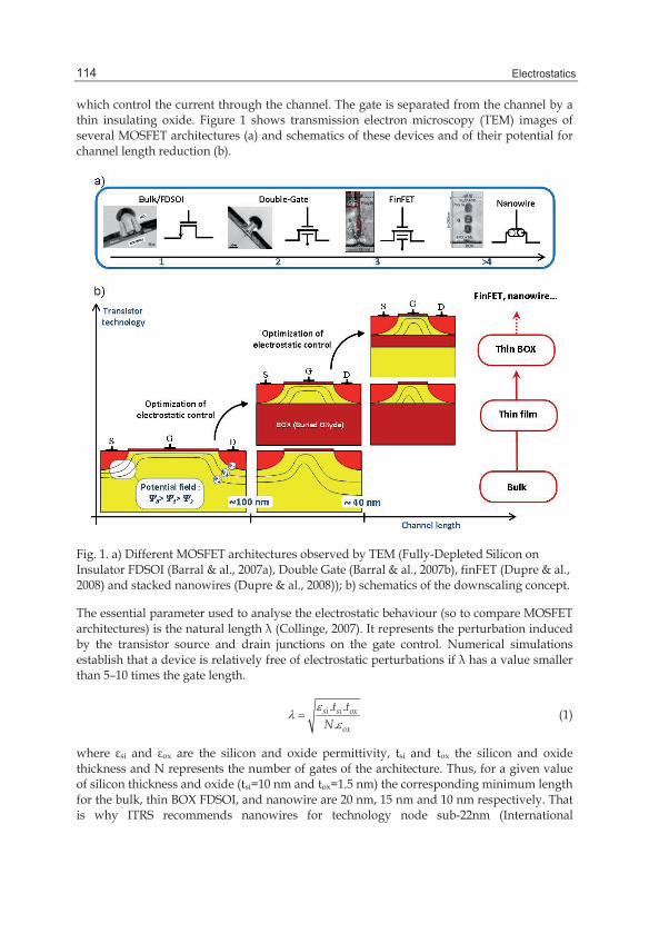
which control the current through the channel. The gate is separated from the channel by a thin insulating oxide. Figure 1 shows transmission electron microscopy (TEM) images of several MOSFET architectures (a) and schematics of these devices and of their potential for channel length reduction (b).
Fig. 1. a) Different MOSFET architectures observed by TEM (Fully-Depleted Silicon on Insulator FDSOI (Barral & al., 2007a), Double Gate (Barral & al., 2007b), finFET (Dupre & al., 2008) and stacked nanowires (Dupre & al., 2008)); b) schematics of the downscaling concept.
The essential parameter used to analyse the electrostatic behaviour (so to compare MOSFET architectures) is the natural length λ (Collinge, 2007). It represents the perturbation induced by the transistor source and drain junctions on the gate control. Numerical simulations establish that a device is relatively free of electrostatic perturbations if λ has a value smaller than 5–10 times the gate length.
. ..
si si ox
ox
t tN
(1)
where εsi and εox are the silicon and oxide permittivity, tsi and tox the silicon and oxide thickness and N represents the number of gates of the architecture. Thus, for a given value of silicon thickness and oxide (tsi=10 nm and tox=1.5 nm) the corresponding minimum length for the bulk, thin BOX FDSOI, and nanowire are 20 nm, 15 nm and 10 nm respectively. That is why ITRS recommends nanowires for technology node sub-22nm (International

Nanowires: Promising Candidates for Electrostatic Control in Future Nanoelectronic Devices
115
Technology Roadmap of Semiconductor [ITRS], 2009) and regarding the advanced processing technologies, the literature provides a wide range of devices based on nanowires, stacked (Dupre & al., 2008), twin (Hwi Cho & al., 2007) or single Ω-FET nanowires (Tachi & al., 2009). In the following, a complete study of the electrostatics of nanowire MOSFETs is performed including all the ultimate physical phenomena which can occur in future electronic devices.
2. The electronic structure of silicon nanowires Standard silicon layers used in microelectronics are crystallographic. Silicon atoms are disposed in a periodical lattice similar to the diamond structure: each atom is tetrahedrally bonded to its four neighbours (see figure 2). The cubic unit cell parameter a0 equals 5.43 Å, corresponding to an interatomic distance of 2.34 Å. Ideal silicon nanowires are thus periodic along their axis, and the length L of their unit cell depends on the crystallographic orientation:
L=a0 for <100> oriented nanowires, L=a0 / 2 for <110> oriented nanowires, L=a0 3 for <111> oriented nanowires.
The orientation and diameter of the nanowire determines its electronic structure, from which result its electrical and optical properties. In the following of this work, we will consider cylindrical nanowires oriented along the <100> axis, as the one represented in figure 2.
The electronic structure of bulk silicon is expressed by the dispersion relations En(k), which give the energy of an electron wavefunction with wavevector k in band n. A schematic of low energy electrons in the conduction band is shown in figure 3. It represents the iso-energy surfaces in the first Brillouin zone (wavevector space). For conduction bands, we can count six energy minima, named the six “Δ valleys” of bulk silicon. Each valley is characterized by an effective mass ml along its orientation axis and mt along its transverse directions. The longitudinal mass is ml equal to 0.919m0 and mt is equal to 0.196m0 where m0 is the free electron mass.
In the following, we consider transport along the x-axis. So, projecting bulk valleys on the nanowire axis (x for the transport, y and z for the perpendicular direction), we can define two different valleys of the nanowire characterized by a conduction and a confinement masses. The valleys 1 and 2 of the figure 3 correspond to the longitudinal valley while the valleys 3, 4, 5 and 6 refer to the transverse valley. The table 1 gives the corresponding masses of the two nanowire valleys. The confinement mass of the transverse valleys is approximated by a “cylindrical mass”, which preserves cylindrical symmetry in the calculations.
Conduction mass Confinement mass Longitudinal valley lm tm
Transverse valley tm 2. .( )
l tl t
m mm m
Table 1. Definition of the longitudinal and the transverse masses for the <100> oriented nanowire.

Electrostatics
116
Fig. 2. Atomistic representation of a <100>-oriented nanowire. Blue: silicon atoms, grey: hydrogen atoms (necessary to passivate the surface in the tight-binding model), red: highlight of the tetrahedral structure of silicon. The nanowire is 1.5nm thick and 5nm long.
Fig. 3. Iso-energy surfaces of the conduction band of bulk silicon in wavevector space, and definition of longitudinal and transverse valleys for transport along a <100>-oriented nanowire.

Nanowires: Promising Candidates for Electrostatic Control in Future Nanoelectronic Devices
117
This effective mass approach is only valid for thick nanowires (diameter > 5 nm) and low electron energy (a few tenths eV). The band structure of silicon is described more accurately by atomistic models, which allow modelling thinner nanowires. A tight-binding model is used here. It consists in developing the wavefunctions on an atomic orbital basis set. The sp3 model developed by (Niquet & al., 2000) is used here and in previous studies (see section 3.4). This model is fitted on first principles calculations based on the density functional theory (DFT) and so-called “GW” corrections for the bandgap. It contains one s orbital and three p orbitals per silicon atom and describes accurately electron (conduction band) and hole (valence band) dispersion relations. When studying nanostructures, the surface is passivated with hydrogen atoms (see figure 2). This model choice is due to the lack of a convenient tight-binding model for the Si/SiO2 interface. Passivation avoids unrealistic surface states and should not modify much the electronic structure of the nanowire. The tight-binding calculations are performed with the code TB_Sim (TBSIM, 2011), which solves the Schrödinger equation in nanostructures containing up to 107 atoms (Niquet & al., 2006). For thin nanowires (diameter < 5 nm), the obtained electronic structure differs from the effective mass calculation (see section 3.4). TB_Sim also allows Poisson-Schrödinger calculations, which give the repartition of the charge density in the nanowire under the influence of the gate voltage. Again, corrections of the effective mass approach are needed for thin nanowires.
3. Modelling of the electrostatics in MOSFETs based on nanowires 3.1 Definition of the threshold voltage
As said previously, the MOSFET transistor is defined by two states (ON or OFF) depending on the voltage applied at the gate. In fact, this polarization creates an electric field in the active region of the transistor which makes carriers concentrate near the interface with the oxide. Increasing the gate voltage, conduction bands start to fill with carriers from lower energy bands to higher energy bands up to saturation. In this regime, the semiconductor is then analog to a metal and forms a conduction layer between contacts (source and drain) of the transistor. Commonly, the threshold voltage is so defined as the frontier of the two states of the transistor and represents its capacity to switch from one state to the other. It is essentially dependent on the electrostatic characteristics. That is why, it is necessary to fully describe the potential ψ everywhere in the device active region. For this purpose, the Poisson equation, given here in cylindrical coordinates, is solved:
² 1 . ( )² A
Si
qd d N ndr r dr
(2)
where NA is the channel doping, n is the electron density, εSi the silicon permittivity, and q the elementary charge. Note that n depends on via the Fermi-Dirac occupation of electronic states.
Two approaches can be used to obtain the solution of such an equation. The first one is the double integration solving (Jimenez & al., 2004; Yu & al., 2007); however the solution is not totally analytical which is not convenient in our case. The second approach is to make an assumption on the potential description along the nanowire radius. In the following, we assume a parabolic potential along the radius of the nanowire cross-section described as:

Electrostatics
118
1 2 3( , ) . . ²r x r r (3)
where the parabolic terms βi are x-dependent functions.
To define these terms, the general expression of the potential (eq. 3) is injected in boundary conditions specific to nanowires (eq. 4): the potential at the position r=D/2 is equal to the potential at the position r=–D/2 (symmetry condition) and is defined as the surface potential ψs:
( / 2, ) ( / 2, ) ( )sD x D x x (4)
Equation (3) becomes:
3 3²( , ) ( ) . . ²
4sDr x x r (5)
0 D/2 D/2+tox-D/2-(D/2+tox)r
Ec
EFi
Ev
EF
Ψs Ψ
VFB
VGS
x
VDS
x x+dx
ζ(x) ζ(x+dx)
ζs
Fig. 4. (a) Schematics of a nanowire device (for a better view the gate oxide and material are not shown), indicating the specific area used in the Gauss law. (b) Band diagram along a vertical cut-line in the nanowire.
The term β3 is found by including (5) into the Poisson equation (2) and integrating along the nanowire radius from 0 to D/2:
,3
.4 .
i linA
Si Si
Qq ND
(6)

Nanowires: Promising Candidates for Electrostatic Control in Future Nanoelectronic Devices
119
where Qi,lin is the charge integrated along the nanowire radius and ψs is the surface potential.
It is important to note that the parabolic assumption is valid at threshold, but could lose its validity in other operation regimes (for example in the strong inversion regime). Figure 4(a) shows the schematics of the nanowire with the longitudinal polarization (VDS) along the x-axis (transport). Figure 4(b) shows the band diagram along a transverse cutline in the nanowire for an applied gate voltage VGS. The potentials are defined with respect to the intrinsic Fermi level as illustrated in figure 4(b).
The starting point of the threshold voltage modelling is the boundary condition at the Si/SiO2 interface:
.SiGS FB S S F
oxV V
C (7)
where VFB is the flat-band voltage, ζS is the electric field at the interface, F is the Fermi potential and Cox is the oxide capacitance in cylindrical coordinates expressed in (Dura & al., 2010).
In our case, we consider the threshold voltage defined as the gate voltage for which the inversion charge reaches its threshold value fixed to (Munteanu & al., 2005):
, .ith lin oxkTQ Cq
(8)
where k is the Boltzmann constant and T is the temperature. Under this condition, the surface potential reaches its threshold value, called ψs,th. The threshold voltage is then obtained as:
,. .Sith FB s th F
oxV V D
C (9)
with
.4 .
A ox
Si Si
q N CkTq D
(10)
In equation (9), only the surface potential is unknown and has to be modeled taking into account the physical phenomena specific to nanowire MOSFETs described below: quantum confinement, short channel effect, and band structure effect.
3.2 Quantum mechanical confinement (QE)
In silicon nanostructures such as nanowires, the wavefunctions related to the different valleys are modified and kinetic energy is quantized along the confinement directions, leading to a set of energy subbands for each valley. Previous works highlight the necessity to consider quantum confinement in the transport modelling of planar architectures (Munteanu & al., 2005), for which the confinement is one-dimensional. For nanowire

Electrostatics
120
devices, quantum confinement is two-dimensional (leading to a 1D electronic gas) and its impact is expected to be stronger (Autran & al., 2005). Figure 5 shows the wavefunction in the first five subbands for the longitudinal valley and for two different nanowire diameters (5 and 10nm). These wavefunctions are calculated using an effective mass Schrödinger-Poisson solver (TBSIM, 2011). The associated energy represents the difference between each energy subband and the first subband level.
Fig. 5. Square modulus of the wavefunction for the five first levels in the longitudinal valley of a 5 and 10nm nanowire diameter. Energy increase of each subband with respect to the first level.
To extract numerically the impact of the diameter on the quantization of carriers, the same calculation has been done for the tranverse valley and for different nanowire diameters. We can note that for low diameters, the quantized levels are higher. So, regarding the targeted MOSFET downscaling to a few nanometers, quantum-mechanical effects have to be

Nanowires: Promising Candidates for Electrostatic Control in Future Nanoelectronic Devices
121
included in the previous analytical model of threshold voltage in order to assess their impact up to circuit performances.
For this purpose, the 1D quantum charge integrated along the radius Qi,lin has to be used:
, ( , , )i lin cj i
Q n E i j (11)
with
1( , , ) 2 ( , ). ( ).c
c D cE
n E i j E E f E dE
(12)
where the factor 2 accounts for the number of equivalent valleys, j is the valley index, i is the subband index, Ec = Eij is the subband bottom energy, ρ1D(E,Ec) is the 1D density-of-states of the subband, and f(E) is the Fermi-Dirac distribution function:
1
21 2
2.1 1( , ) . .D cc
mjE EE E
(13)
1( )1 exp F
f EE E
kT
(14)
where mj is the 1D density-of-states effective mass in valley j and EF is the Fermi level. The general expression of the charge is then:
0.5
,0 2
21( . ( ). ). . .²
1ij S
ji lin q Eg
r Ej i kT
m kT rQ q g j drq
e
(15)
Under non-degenerate condition (valid at threshold), the Fermi-Dirac distribution can be approximated by a simple exponential (corresponding to the Boltzmann distribution). The expression of the charge becomes (Autran & al., 2004):
.
*, .
SqkT
i linQ Q e
(16)
with
( )* 2
21( . ( ). ). . .²
ij
q EgEj kT
j i
m kTQ q g j eq
(17)
where Eg is the silicon bandgap, and g(j) is the degeneracy of the valley j (equal to 2 for each valley). The charge is then obtained by a sum over the different silicon valleys (index j) and a sum over all quantized levels (index i) of each valley (in practice limited to 5). The quantum energy levels are needed in (17) and have to be calculated analytically. For a

Electrostatics
122
cylindrical cross-section of the nanowire, the analytical expressions of the transversal (index t) and longitudinal (index l) quantum energy levels are given by (Baccarani, 2008):
1,2
3
( . . )² 1 1.( )4. .( / 2)²( . . )² 1.
2. .( /2)²
i it
t l
i il
t
iE Eq D m m
iE Eq D m
(18)
where α is a numerical parameter (Baccarani, 2008). We can note a good agreement between (18) with α=2.1 and a self-consistent cylindrical 1D Schrödinger-Poisson solver (ATLAS, 2010) for the first energy level (transversal and longitudinal) (Dura & al., 2010).
From equation (16), the surface potential at threshold voltage is given by:
,, *.ln( )ith lin
s thQkT
q Q (19)
with Qith,lin the inversion charge at threshold defined by (8).
0
0.1
0.2
0.3
0.4
0.5
0.6
0.7
0 5 10 15 20
Analytical modelNumerical simulation
Vth
,q -
Vth
,cl (
V)
Diameter D (nm) Fig. 6. Threshold voltage shift between quantum (Vth,q) and classical (Vth,cl) approaches versus nanowire diameter in long channel transistors. Comparison between the analytical model and data obtained from Schrödinger-Poisson numerical solving (ATLAS, 2010).
Including this expression in (9), the quantum threshold voltage for long channel transistor is easily obtained. Figure 6 plots the difference between quantum and classical threshold voltage versus the nanowire diameter; as expected, this difference increases when reducing the nanowire diameter, due to a stronger quantization of carrier energy when the nanowire

Nanowires: Promising Candidates for Electrostatic Control in Future Nanoelectronic Devices
123
diameter is reduced. Figure 6 also shows a very good agreement between the analytical model and data obtained by a Schrödinger-Poisson numerical solving (ATLAS, 2010).
3.3 Short-Channel Effect (SCE)
As said in the introduction, the downscaling of transistor is required. That is why the gate length is continuously reduced. However, from a certain dimension, the transistor junctions (source and drain) have an impact on the electrostatic control of the device. Previously 1D (only the gate voltage), it becomes 2D because gate and drain polarizations compete to control the device. And this strongly affects the device characteristics. Thus, MOSFET architectures are considered to be impacted by the short channel effect when the channel length is the same order of magnitude as the depletion-layer widths of the source and drain junction. The main result is the modification of the threshold voltage (or the loss of electrostatic control) due to the shortening of the channel length. It is attributed to two phenomena: SCE (Short Channel Effect) and DIBL (Drain Induced Barrier Lowering). The first one is coming from the superposition of the depletion-layer widths of the source and drain junction. The second phenomenon is a secondary effect on the charge sharing due to higher drain voltage. Nanowire transistors being expected for ultimate technology node, consideration of short channel effect is required in a realistic modeling of this architecture.
To fully describe 2D electrostatic effects (SCE and DIBL) in short channel devices, we propose a full analytical model describing the threshold voltage impacted by SCE and DIBL. The x-dependence (transport direction) of the surface potential has to be know. Applying the Gauss law on a nanowire slice as illustrated in figure 4(a), the following equation is obtained (Munteanu & al., 2005):
22 2 . . .( ). . ( ). . ( ). . .
4 4 4.A
SSi
q N DD Dx x dx x D dx
(20)
where ζ is the electric field expressed by:
( )( ) . Sd xxdx
(21)
η is a fitting parameter which models the lateral electric field variation (Banna & al., 1995). It depends on the channel doping, the channel length, the nanowire diameter and the polarization. An empirical formula for η, obtained from numerical simulations, will be presented below to include these both effect. Introducing (21) in (20), we find a second order equation for the surface potential:
² 24 . [ . . 2 ( )]² . . . . 2
s oxs A ox GS FB F
Si Si
d C Dq N C V Vdx D D
(22)
The solution of this equation is given by (Munteanu & al., 2005):
. . 31 2. .
²4.. .
x xs
ox
Si
KK e K e
CD
(23)

Electrostatics
124
where K1, K2 and K3 are functions resulting from the Poisson equation solving:
. 32
1
(1 ).( )
2. ( . )
cLb DS
c
Ke V VK
sh L
(24)
. 32
2
(1 ).( )
2. ( . )
cLb DS
c
Ke V VK
sh L
(25)
32 [ . . 2 ( )]
. . 2
A ox GS FB F
Si
DK q N C V VD
(26)
where Vb is the built-in potential depending on the channel doping NA, the source/drain doping NSD and the intrinsic carrier density ni as:
2..ln A SD
bi
N NkTVq n
(27)
The position where the surface potential is minimum xmin and the value of ψS (ψs,min) at the position xmin are obtained by forcing the first derivative of equation (23) to be equal to zero (Munteanu & al., 2005):
2min
1
1 .ln( )2.
KxK
(28)
3,min 1 2 22 .s s
KK K
(29)
We assume that the transistor switches on when ψs,min= ψs,th. By inserting this expression in the general expression of the threshold voltage (9), we obtain:
31 22. . 2 .
Si
th FB Fox
KV V D K KC
(30)
We can, by analogy to (Suzuki & al., 1996), distinguish two different terms. The first one (independent from the channel length) refers to the long-channel threshold voltage Vth,long; the second term, which tends to zero for long channel length, represents the threshold voltage roll-off and describes the impact of SCE/DIBL:
3, 2. .
Si
th long FB Fox
KV V DC
(31)
1 22 .thV K K (32)
where the variation of the threshold voltage is defined as:

Nanowires: Promising Candidates for Electrostatic Control in Future Nanoelectronic Devices
125
th th th,longV V V (33)
At threshold, VGS=Vth in (26) and, considering (33), K3 will depend on ΔVth. Moreover K1 and K2 depend on K3, they will also depend on ΔVth. Then, developing (33) leads to a second order equation of ΔVth as:
2. . 0th thA V B V C (34)
with
2
42
4 4
,
. 2.[1 . ]2.[1 . ].[2. ]
2. .[1 . ].[ ]
C C
C DS
C DS DS
b th long FB F
A sh L ch LB ch L H V
C H ch L H V VD V V V
(35)
Finally, the threshold voltage roll-off is the solution of (34) given by:
2 4. .
2.thB B A CV
A
(36)
We can note that to find this term, we have to take into account the long-channel threshold voltage (see coefficient D in eq.35) which includes the dependence on the quantum confinement. Consequently, this model includes both the impact of quantum confinement on the long channel and the threshold voltage roll-off. The most common model (such as references (Banna & al., 1995; Suzuki & al., 1996)) does not include the effect of quantum confinement on the evolution of the short channel effect in analytical modeling which becomes dominant in nanoscale device such as nanowire (this aspect will be detailed later in paragraph 4).
-0.5
-0.4
-0.3
-0.2
-0.1
0
0.1
0 5 10 15 20 25 30 35 40
Analytical modelNumerical simulation
VDS
=0.5V
VDS
=50mV
Thre
shol
d vo
ltage
roll-
off
(V)
Channel Length LC (nm)
Diameter 5nm
Fig. 7. Threshold voltage roll-off versus channel length for low (VDS=50mV) and high (0.7V) drain voltage obtained by the analytical model and TCAD simulations for a 5 nm nanowire diameter; tox=1 nm.

Electrostatics
126
The threshold voltage roll-off is represented in figure 7 for nanowire diameters of 5 nm (calculated in the classical case, i.e. without quantum confinement). TCAD numerical simulations have been done for a cylindrical structure using a drift-diffusion model in order to obtain drain current characteristics as a function of the gate voltage. The threshold voltage is extracted from these current-voltage characteristics using the classical constant current method. The threshold voltage data extracted from TCAD simulations for different diameters have been used to derive an empirical expression of the parameter η including the dependence on the channel length, nanowire diameter and drain to source voltage:
21 2
0. . .DS C C
D V f L f Lf D
(37)
where f0, f1 and f2 are constant fitting parameters, calibrated on numerical simulations. Equation (37) is valid for a wide range of nanowire diameter (down to 2 nm) and channel lengths (down to channel length equal to the nanowire diameter). The results in figure 7 show a good agreement between the analytical model and threshold voltage data obtained from TCAD simulations.
3.4 Band Structure Effect (BSE)
Advanced atomistic numerical simulations (Neophytou & al., 2008; Niquet & al., 2000, 2006; Sarrazin & al., 2009; Nehari & al., 2006) have shown that a strong reduction of the silicon thickness impacts the material properties by modifying the band structure. Indeed, the dimensions targeted in ultra-scaled devices are those of a few tens atomic layers (several nanometers). At these dimensions, the electronic properties differ from the calculations shown in section 3.2 and based on the bulk effective masses. In (Sarrazin & al., 2009), atomistic tight-binding (TB) Schrödinger-Poisson simulations have been performed for the case of [001] oriented silicon nanowire in order to highlight the variation of the band structure with the nanowire diameter. The code TB_Sim (TBSIM, 2011) has been used with a sp3 tight-binding model (Niquet & al., 2000). Figure 8 shows the valence and the conduction bands for Si nanowire width of 2nm and 10nm. We can note that when thinning the silicon film the minimum of the conduction band is increased and the general shape of bands becomes smoother (Sarrazin & al., 2009). However, the bandgap increase is smaller than the effective mass result of section 2.4.
In order to include these modifications in the previous threshold voltage modelling, analytical expressions of parameters affected by the band structure effect (band gap and effective masses) are proposed here. Diameter-dependent analytical functions (fitted on numerical simulations as illustrated in figure 9) are found for the bandgap and effective masses (inspired from (Niquet & al., 2000):
1, 2
1 1.g g bulkKE E
D A D B
(37)
2( ) ( ), 2
2 2.t l t l bulkKm m
D A D B
(38)
where A, B and K are fitting constants.

Nanowires: Promising Candidates for Electrostatic Control in Future Nanoelectronic Devices
127
1.5
2
2.5
0 0.1 0.2 0.3 0.4
Ene
rgy
(eV
)
-1.4
-1.2
-1
-0.8
-0.6
-0.4
-0.2
0
0 0.1 0.2 0.3 0.4
Ener
gy (
eV)
k (x 2/L)
1.1
1.15
1.2
1.25
1.3
1.35
1.4
0 0.1 0.2 0.3 0.4
Ener
gy
(eV)
-0.25
-0.2
-0.15
-0.1
-0.05
0
0 0.1 0.2 0.3 0.4
Ene
rgy
(eV
)
k (x 2 /L)
D=2nm D=10nm
conduction
valence
Fig. 8. Silicon nanowire band structure obtained with a tight-binding Schrödinger-Poisson solver (TBSIM, 2011) for two different diameters (2 and 10 nm). Up: Conduction band; down: Valence band.
0.9
0.95
1
1.05
1.1
1.15
1.2
1.25
0.15
0.2
0.25
0.3
0.35
0.4
0 5 10 15 20
ModelNumerical SimulationAnalytical modelNumerical simulation
Rel
ativ
e lo
ngitu
dian
al m
ass R
elative transversal mass
Diameter D (nm)
1
1.5
2
2.5
3
3.5
4
0 5 10 15 20
Analytical modelNumerical simulation
Ban
d ga
p (e
V)
Diameter D (nm) Fig. 9. Variation of the silicon band gap (a) and relative longitudinal and transversal masses (b) with respect to the silicon nanowire diameter. Comparison with atomistic simulations obtained in (Sarrazin & al., 2009).

Electrostatics
128
4. Results and discussion We have just presented the modeling of all the physical phenomena which affect the electrostatics of nanowire MOSFETs. In this part, the impact of each mechanism is assessed at different levels of interest: threshold voltage, drain current and small-circuits performance.
4.1 Impact on the threshold voltage
4.1.1 Long-channel transistors
Figure 10 shows the long-channel threshold voltage increase due to quantum confinement, without BSE (i.e., considering bulk value for the band gap and the conduction masses) and with BSE (i.e., considering equations (37) and (38)). The analytical model has been compared to both numerical simulations (Sarrazin & al., 2009) and experimental data (Suk & al., 2007).
0
0.1
0.2
0.3
0.4
0.5
0.6
0.7
0 2 4 6 8 10 12 14
Analytical modelNumerical simulationExperimental data
Vth
,q -
Vth
,cl
(V)
Diameter D (nm)
without Band Structure effects
with Band Structure effects
Fig. 10. Difference between quantum (Vth,q) and classical threshold voltage (Vth,cl) with and without BSE versus nanowire diameter (long channel transistors). Comparison between the analytical model, atomistic simulations (Sarrazin & al., 2009) and experimental data (Suk & al. 2007).
We can note that the band structure effects tend to limit the impact of the quantum confinement on the threshold voltage of the nanowire. This is coherent with equation (18). Increasing the effective masses, the quantum energy levels are lowered and the energy quantization decreases; then the quantum threshold voltage is lower. Figure 10 highlights the importance of considering BSE especially for thin film where the difference between threshold voltage with BSE and threshold voltage without BSE increases when reducing the nanowire diameter.

Nanowires: Promising Candidates for Electrostatic Control in Future Nanoelectronic Devices
129
4.1.2 Short-channel transistors
In the following, we investigate the impact of the quantum confinement on SCE, then the impact of BSE on SCE. As stated previously, the threshold voltage roll-off depends on quantum confinement through the long-channel threshold voltage which includes quantum confinement effects.
-0.3
-0.25
-0.2
-0.15
-0.1
-0.05
0
0 5 10 15 20
ClassicalQuantumQuantum + BSENumerical simulation
Thre
shol
d vo
ltage
roll-
off
(V)
Diameter D = Channel length LC
LC=D
VDS
=0.5V
Fig. 11. Impact of band structure variations on SCE. Threshold voltage roll-off versus nanowire diameter for a channel length equal to the nanowire diameter. Comparison with data extracted from numerical simulations using a cylindrical Schrödinger-Poisson solver (Munteanu & Autran, 2003).
Figure 11 shows the impact of quantum effect and BSE on SCE as a function of the nanowire diameter. The curves plot the threshold voltage roll-off for a channel length equal to the nanowire diameter for the three approaches: classical (i.e., without quantum confinement and BSE), quantum without BSE, and quantum with BSE. Quantum threshold voltage obtained using the analytical model is validated in Fig. 11 with numerical simulation data obtained with a cylindrical Schrödinger-Poisson solver (Munteanu & Autran, 2003; Zervos & Feiner, 2004). We can note that the quantum confinement tends to limit SCE. This is due to the enhanced electrostatics control of the active area due to carrier energy quantization. As expected, the difference between quantum and classical approaches increases when reducing the nanowire diameter (due to the increase of energy quantum level for thinner films). When considering quantum confinement, the carrier energy is higher than for classical approach. That is why it is less affected by the longitudinal source to drain electric field, which generally strongly impacts the transistors performances at these channel length values. Moreover, figure 11 shows that BSE tend to amplify the impact of quantum effects on SCE: the threshold voltage roll-off is reduced when considering quantum confinement with BSE compared to the case when only quantum confinement is considered. For long channels, the threshold voltage decrease when considering BSE was due to the increase of

Electrostatics
130
the effective masses which lowered the quantized levels. In the case of short channels, the reduction of SCE when BSE are taken into account is the consequence of the band gap increase. A wider band gap means a higher energetic barrier, leading to a better electrostatics control which is less impacted by source-channel and drain-channel junctions when reducing the nanowire channel length. Moreover, we can note that below a certain diameter (depending on the modeling approach), the diameter thinning has a stronger impact on the threshold voltage roll-off than the channel length reduction. For the same channel length to diameter ratio, the threshold voltage roll-off is higher for D=5 nm than for D=2 nm. Indeed, for ultra-thin films, the quantization of carrier energy is very strong and the carrier concentration is mainly controlled by quantum confinement. In the case of D=2 nm, the strong electrostatic control due to the ultra-thin diameter completely overcomes the increase of SCE expected for these ultra-short channel lengths.
4.2 Impact on the injection velocity
Another parameter affected by the BSE is the thermal velocity which depends on masses along the transport direction. Indeed, in our case, for a transport along the (001) direction, the expression of thermal velocity is:
2..th
t
kTvm
(39)
Figure 12 (Dura & al., 2011) shows the thermal velocity evolution with respect to the nanowire diameter. We can note a non-negligible reduction for ultra-thin nanowires up to a 20% decrease for D = 2 nm.
8.5
9
9.5
10
10.5
11
11.5
12
12.5
4 8 12 16 20
With band structure effectWithout band structure effect
Ther
mal
vel
ocity
(10
4 m/s
)
Diameter D (nm) Fig. 12. Impact of the band structure effect on the thermal velocity with respect to the silicon nanowire diameter.

Nanowires: Promising Candidates for Electrostatic Control in Future Nanoelectronic Devices
131
4.3 Impact on ballistic drain current of nanowire MOSFET
In previous works, we have demonstrated the analytical model of drain current in GAA nanowire MOSFETs in the ballistic transport regime (without interactions). We remind that this ballistic drain current is derived from the flux method initiated by McKelvey et al (McKelevey & al., 1961), doing a balance in the active region between the different carrier fluxes. In the degenerate case, the ballistic drain current is given by the following expression:
0
0 0
112
2
12
.( )1
( ) ( ). . .( ). . .( ).( ) ( )1
( )
DSF
F FD ox GS t th
DSFF
F
q VkT
I D C V V v q VkT
(40)
where D is the nanowire diameter, vth is the thermal velocity discussed above, VGS is the drain to source voltage, VDS is the drain to source voltage, Cox is the oxide capacitance, ηF is the Fermi level, 0 and 1/2 are the Fermi integral of order 0 and -1/2 respectively and Vt is the threshold voltage modeled above.
10-12
10-10
10-8
10-6
10-4
0 0.2 0.4 0.6 0.8 1
QE with BSE
QE without BSE
Numerical simulations
Bal
listic
dra
in c
urre
nt (
A)
Gate Voltage (V)
D=5nm
D=3nm
Lc=20nm
VDS
=0.4V
Fig. 13. Impact of the band structure effect on the ballistic drain current. Comparison with numerical simulations (deterministic Wigner equation solving (Barraud & al., 2009)).
Figure 13 shows the result at the device level for a long channel transistor and for two different nanowire diameters (3 and 5nm) (Dura & al., 2011). The ballistic drain current model is compared to numerical simulations based on a deterministic Wigner equation solver (Barraud & al., 2009). We can note a strong impact of BSE on the current in the sub-

Electrostatics
132
threshold regime for 3nm-diameter due to the Vt variation while the ON-state current stays almost unchanged. From this graph, we can highlight the necessity to take into account the correction due to bands variations in the modeling if we expect to provide predictive devices performances. Indeed, at 3nm, the off-state current is increased by more than one decade when BSE is considered.
4.4 Impact on performances of small circuits based on nanowire MOSFETs
After implementation in a Verilog-A environment, the model presented above has been used to simulate a CMOS inverter and then a complete 11 stages-ring oscillator. In order to build-up the CMOS inverter a p-type nanowire MOSFET is considered symmetrically to the n-type transistor in the inverter setup. The impact of BSE can be addressed at the circuit level through the study of the commutation characteristics of the inverter or the oscillation frequency of a ring oscillator.
Figure 14 shows the input/output characteristics of the inverter for the classical case (i.e., without QE), with quantum effects (QE) and with band structure effects (QE+BSE). We can note that the inverter characteristic is more abrupt when considering only QE. Similarly to the results obtained for the threshold voltage, BSE tends to limit the impact of quantum confinement by smoothing the CMOS inverter switch.
Vdd
Vin Vout
0
0.2
0.4
0.6
0.8
1
0 0.2 0.4 0.6 0.8 1
ClassicalQEQE+BSE
Vout
(V
)
Vin (V)
Vdd=1VLc=20nmD=3nm
0.9
0.92
0.94
0.96
0.98
1
0.45 0.46 0.47 0.48 0.49
Fig. 14. Impact of BSE on the inverter characteristic. Comparison between classical (i.e, without QE), quantum (QE) and low dimensions effects (QE+BSE).
Regarding the ring oscillator, the results seem opposite to the inverter case. The better performances are for the classical case and introducing quantum confinement reduces the oscillation frequency. This is due to the fact that the ring-oscillator frequency is directly proportional to the ON-state current in strong inversion regime Vdd=1.5V (far from the threshold voltage). QE increases Vth and consequently reduces the current. The injection velocity also impacts directly the current and then the oscillation frequency is affected. The result is a reduction of the oscillation frequency when BSE are taken into account.

Nanowires: Promising Candidates for Electrostatic Control in Future Nanoelectronic Devices
133
1 1 1CL
1
10
2 3 4 5 6 7 8 9 10
ClassicalQEQE+BSE
Vdd=1.5VLc=30nm
Diameter D (nm) Fig. 15. Impact of BSE on the ring oscillator frequency versus the nanowire diameter. Comparison between classical, quantum (QE) and low dimensions effects (QE+BSE).
5. Conclusion In this chapter, the potential of silicon nanowires for microelectronics applications was evaluated. Regarding the evolution of transistor architectures, they appear as the best configuration for the gate control of the device. The particular shape with a surrounding gate provides an ideal electrostatic control to immunize transistors against perturbations generated by the scaling down of dimensions. In this work, we have developed a complete model of the electrostatic of transistors based on nanowires. The physical phenomena affecting the electrostatics was considered: short-channel effects due to the channel length reduction or the quantum mechanical effects due to the diameter thinning. Moreover, ultimate mechanisms as the modification of the band shape of silicon material is studied based on advanced simulations (essentially tight-binding Schrodinger-Poisson solving). All this physics (thanks to analytical model development) is transposed to higher simulation levels as characteristics of transistor or small-circuit performances. Following this idea, we have seen the impact of short-channel, quantum or band structure effect on the threshold voltage. For ultra-thin nanowires, we highlighted the necessity to consider all these phenomena to be as close as possible to experimental data. Then, a study of their impact on transport was performed with the analysis of ballistic drain current of single transistor and performances of inverters or ring oscillators. In all cases, the evaluation of performances is inaccurate if quantum or band structure effects are not considered. For example, one decade and a half of difference on OFF-state current or a reduction of factor 2 or 3 on the oscillation frequency show the importance of the electrostatics (and so a realistic modeling) if we envisage nanowires as the future technological solution in microelectronics.
6. References ATLAS. (2010). Users Manual, SILVACO, 2010. Autran, J.L.; Munteanu, D.; Tintori, O.; Harrison, S.; Decarre, E. & Skotnickin, T. (2004).
Quantum-mechanical analytical modeling of threshold voltage in long-channel

Electrostatics
134
double-gate MOSFET with symmetric and asymmetric gates, Proceedings of 7th Int. Conf. Modeling and Simulation of Microsystems, MSM’2004, pp. 163-166, ISBN 0-9728422-8-4, Boston, Massachusets, USA, March 07-11, 2004
Autran, J.L.; Nehari, K. & Munteanu, D. (2005). Compact modeling of the threshold voltage in silicon nanowire MOSFET including 2D-quantum confinement effects, Molecular Simulation, Vol. 31, No. 12, (October 2005), pp. 839-843, 0892-7022
Baccarani, G. (2008). Device Physics for the Modeling of Future Nanoscale Silicon Devices, Proceedings of SINANO Summer School on Device Modeling, Bertinoro, Italy, September 1-5, 2008
Banna, S.R.; Chan, P.C.H.; Ko, P.K.; Nguyen, C.T. & Chan, M. (1995). Threshold voltage model for deep-submicrometer fully depleted SOI MOSFETs, IEEE Trans. Electron Devices, Vol. 11, No. 5, (April 1995), pp. 487-495, 0026-2714
Barral, V.; Poiroux, T.; Andrieu, F.; Faynot, O. ; Ernst, T.; Brevard, L.; Fenouillet-Beranger, C.; Lafond, D. ; Hartmann, J.M.; Vidal, V.; Allain, F.; Daval, N.; Cayrefourcq, I.; Tosti, L. ; Munteanu, D.; Autran, J.L. & Deleonibus, S. (2007). Strained FDSOI CMOS technology scalability down to 2.5nm film thickness and 18nm gate length with a TiN/HfO2 gate stack, Proceedings of IEDM Tech. Dig., pp. 61-64, ISBN 978-1-4244-1507-6, Washington, USA, December 10-12, 2007
Barral, V.; Poiroux, T.; Vinet, M.; Widiez, J. ; Previtali, B.; Grosgeorges, P.; Le Carval, G.; Barraud, S.; Autran, J.L.; Munteanu, D. & Deleonibus, S. (2007). Experimental determination of the channel backscattering coefficient on 10-70 nm-metal-gate, Double-Gate transistors, , Solid State Electron., Vol. 51, No. 4,(April 2007), pp. 537-542, 0038-1101
Barraud, S.; Bonno, O. & Cassé, M. (2009). Phase-coherent quantum transport in silicon nanowires based on Wigner transport equation: Comparison with the nonequilibrium-Green-function formalism, Journal of Applied Physics., Vol. 106, No. 6, (September 2009) 0021-8979
Collinge, J.P. (2007). Multiple-gate SOI MOSFETs, Solid State Electron., Vol. 48, No. 9, (September 2007), pp. 2071-2077, 0038-1101
Dupre, C.; Hubert, A.; Becu, S.; Jublot, M.; Maffim-Alvaro, V. & Vizioz, C. (2008). 15nm-diameter 3D stacked nanowires with independent gates operation: ΦFET, Proceedings of IEDM Tech. Dig., pp. 749-752, ISBN 978-1-4244-2377-4, San Francisco, California, USA, December 15-17, 2008
Dura, J.; Martinie, S.; Munteanu, D.; Jaud, M.A.; Barraud, S. & Autran, J.L. (2010). Analytical model of quantum threshold voltage in short-channel nanowire MOSFET including band structure effects, Proceedings of NSTI-Nanotech WCM, Vol. 2, pp.801-804, ISBN 978-1-4398-3402-2, Anaheim, California, USA, June 21-24, 2010
Dura, J.; Martinie, S. ; Munteanu, D. ; Triozon, F. ; Barraud, S. ; Niquet, Y.M. ; Barbé, J.C. & Autran, J.L. (2011). Analytical model of ballistic current for GAA nanowire MOSFET including band structure effects: Application to ring oscillator, Proceedings of 2011 Ultimate Integration of Silicon, ISBN 978-1-4577-0089-7, Cork, Ireland, March 14-16, 2011
Hwi Cho, K.; Suk, S.D.; Yeoh, Y.Y.; Li, M.; Yeo, K.H.; Kim, D.W.; Park, D.; Lee, W.S.; Jung, Y.C.; Hong, B.H. & Sung Woo H. (2007). Temperature-dependent characteristics of cylindrical gate-all-around twin silicon nanowire MOSFETs (TSNWFETs). IEEE Electron Devices Letters, Vol. 28, No. 12, (December 2007), pp. 1129-1131, 0741-3106

Nanowires: Promising Candidates for Electrostatic Control in Future Nanoelectronic Devices
135
ITRS. (2009). In: International Technology Roadmap for Semiconductors, 05.08.2011, Available from: http://www.itrs.net/Links/2009ITRS/Home2009.htm
Jimenez, D.; Iniguez, B.; Sune, J.; Marsal, L.F.; Pallares, J.; Roig, J. & Flores, D. (2004). Continuous analytic I-V model for surrounding-gate MOSFETs, IEEE Electron Device Lett., Vol. 25, No. 8, (August 2004), pp. 571-573, 0741-3106
McKelevey, J.P.; Longini, R.L. & Brody, T.R. (1961). Alternative approach to the solution of added carrier transport problems in semiconductors, Physical Review, Vol. 123, No. 1, (July 1961), pp. 2736-2743, 0010.1103
Munteanu, D. & Autran, J.L. (2003). Two-dimensional Modeling of Quantum Ballistic Transport in Ultimate Double-Gate SOI Devices, Solid State Electron., Vol. 47, No. 7, (July 2003), pp. 1219-1225, 0038-1101
Munteanu, D.; Autran, J.L.; Harrison, S.; Nehari, K.; Tintori, O. & Skotnicki, T. (2005). Compact model of the quantum short-channel threshold voltage in symmetric Double-Gate MOSFET, Molecular Simulation, Vol. 31, No. 12, (July 2005), pp. 1911-1918, 0022-3093
Nehari, K.; Cavassilas, N.; Autran, J.L.; Bescond, M.; Munteanu, D. & Lannoo, M. (2006). Influence of band structure on electron ballistic transport in silicon nanowire MOSFET's: An atomistic study, Solid State Electron., Vol. 50, No. 4, (April 2006), pp. 716-721, 0038-1101
Neophytou, N.; Klimeck, G. & Lundstrom, M.S. (2008). Bandstructure effects in silicon nanowire electron transport, IEEE Trans. Electron Devices, Vol. 43, No. 5, (June 2008), pp. 732-738, 0018-9383
Niquet, Y.M.; Delerue, C.; Allan, G. & Lannoo, M. (2000). Method for tight-binding parametrization: Application to silicon nanostructures, Physical Review B, Vol. 62, No. 8, (August 2000), pp. 5109-5116, 0163-1829
Niquet, Y.M.; Lherbier, A.; Quang, N.H.; Fernández-Serra, M.V.; Blase, X. & Delerue, C. (2006). Electronic structure of semiconductor nanowires, Physical Review B, Vol. 73, No. 16, (April 2006), pp. 5319-5332, 1098-0121
Sarrazin, E.; Barraud, S.; Triozon, F. & Bournel, A. (2008). A self-consistent calculation of band structure in silicon nanowires using a Tight-Binding model, Proceedings of SISPAD, No. 5, pp. 349-352, ISBN 978-1-4244-1753-7, Hakone, Japan, September 9-11, 2008
Suk, S.D.; Lee, S.Y.; Kim, S.M.; Yoon, E.J. & Kim, M.S. (2007). Investigation of nanowire size dependancy on TSNWFET, Proceedings of IEDM Tech. Dig., pp. 891-894, ISBN 978-1-4244-1507-6, Washington, USA, December 10-12, 2007
Suzuki, K.; Tosaka, Y. & Sugii, T. (1996). Analytical threshold voltage for short channel n+-p+ double-gate SOI MOSFETs, IEEE Trans. Electron Devices, Vol. 43, No. 5, (July 1996), pp. 1166-1168, 0018-9383
Tachi, K.; Casse, M.; Jang, D.; Dupre, C.; Hubert, A.; Vulliet, N.; Maffini-Alvaro, V. ; Vizioz, C.; Carabasse, C.; Delaye, V.; Hartmann, J.M.; Ghibaudo, G.; Iwai, H.; Cristoloveanu, S.; Faynot, O. & Ernst, T. (2009). Relationship between mobility and high-k interface properties in advanced Si and SiGe nanowires, Proceedings of IEDM Tech. Dig., pp. 313-316, ISBN 97-4244-5640-6, Baltimore, USA, December 7-9, 2009
TBSIM. (2011). In: TB-SIM homepage, 04.10.2011, Available from: http://inac.cea.fr/L_Sim/TB_Sim/index.html

Electrostatics
136
Yu, B.; Lu, H.; Liu, M. & Taur, Y. (2007). Explicit continuous models for double-gate and surrounding-gate MOSFETs, IEEE Trans. Electron Devices, Vol. 54, No. 10, (October 2007), pp. 2715-2722, 0018-9383
Zervos, M. & Feiner, L.F. (2004). Electronic structure of piezoelectric double-barrier InAs/InP/InAs/InP/InAs (111) nanowires, Journal of Appl. Phys., Vol. 95, No. 1, (January 2004), pp. 281-291, 0021-8979

© 2012 The Author(s). Licensee IntechOpen. This is an openaccess article distributed under the terms of the Creative CommonsAttribution 3.0 License, which permits unrestricted use, distribution,and reproduction in any medium, provided the original work isproperly cited.