constraint-driven design - the next step towards … „constraint-driven design - the next step...
TRANSCRIPT

„Constraint-driven Design - The Next Step Towards Analog Design Automation“, ISPD’09, 2009/03/31 1
Jens Lienig Dresden University of Technology, IFTE Dresden, Germany Email: [email protected]
Constraint-driven Design - The Next Step Towards Analog Design
Automation
Invited Talk
Göran Jerke Robert Bosch GmbH, AE/EIM Reutlingen, Germany Email: [email protected]

„Constraint-driven Design - The Next Step Towards Analog Design Automation“, ISPD’09, 2009/03/31 2
?
Motivation
Evolution of Analog IC Design
Polygon Pushing
Technology
Schematic
1980 1990 2000
DRC
LVS
Schematic- driven Layout
Analog Design Synthesis
2010
Verification of...
Constraint- driven Design
today

„Constraint-driven Design - The Next Step Towards Analog Design Automation“, ISPD’09, 2009/03/31 3
Contents
The verification gap
Current approaches for constraint consideration
The constraint-driven design flow
Impact on design algorithms and design flow Open problems
Summary and conclusion

„Constraint-driven Design - The Next Step Towards Analog Design Automation“, ISPD’09, 2009/03/31 4
Contents
The verification gap
Current approaches for constraint consideration
The constraint-driven design flow
Impact on design algorithms and design flow Open problems
Summary and conclusion

„Constraint-driven Design - The Next Step Towards Analog Design Automation“, ISPD’09, 2009/03/31 5
Secondary Constraints
Primary Constraints
The Verification Gap Constraint Classification
Technology Constraints (manufacturing) min. wire width, spacing, overlap
Functional Constraints (circuit function) max. IR-drop between two net terminals, device matching, ...
Design-Methodical Constraints (design complexity) Design hierarchy, routing directions, standard cells
Economic Constraints (cost, TTM) Chip count, development costs and chip area determine IC technology
„Constraint-driven Design - The Next Step Towards Analog Design Automation“, ISPD’09, 2009/03/31 6
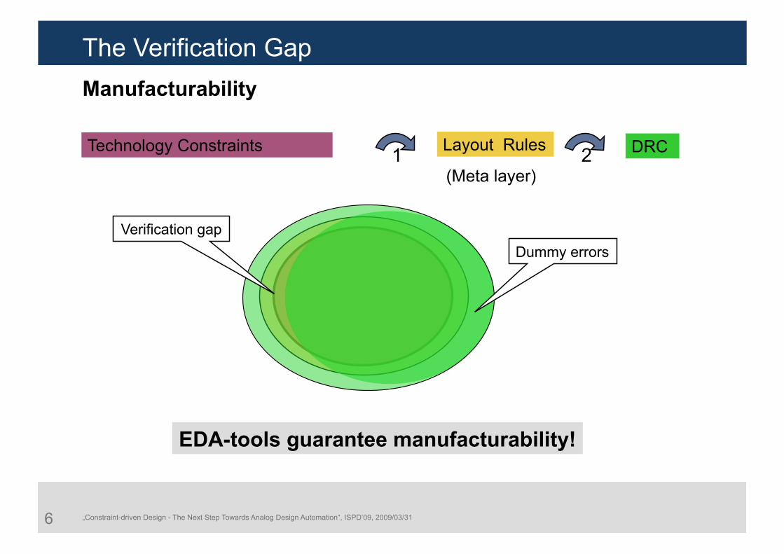
The Verification Gap Manufacturability
Layout Rules 2
EDA-tools guarantee manufacturability!
DRC Technology Constraints 1 (Meta layer)
Dummy errors Verification gap

„Constraint-driven Design - The Next Step Towards Analog Design Automation“, ISPD’09, 2009/03/31 7
The Verification Gap Functionality
Schematic 2
EDA-tools do not (yet) guarantee circuit functionality !
LVS Functional Constraints 1 (Meta layer) (Expert knowledge)
Unrepresentable expert knowledge
Representable, but non-verifiable knowledge
(schematic prosa, symmetries, …)
Devices, parameters,
nets

„Constraint-driven Design - The Next Step Towards Analog Design Automation“, ISPD’09, 2009/03/31 8
The Verification Gap Evolution of Analog IC Design
Polygon Pushing
Technology
Schematic
1980 1990 2000
DRC
LVS
Schematic- driven Layout
Constraint- driven Design
Analog Design Synthesis
2010
Verification of... Constraints / Expert Knowledge
Constraint Verification
today

„Constraint-driven Design - The Next Step Towards Analog Design Automation“, ISPD’09, 2009/03/31 9
Contents
The verification gap
Current approaches for constraint consideration
The constraint-driven design flow
Impact on design algorithms and design flow Open problems
Summary and conclusion

„Constraint-driven Design - The Next Step Towards Analog Design Automation“, ISPD’09, 2009/03/31 10
Current Approaches for Constraint Consideration Constraint-Consideration during Schematic Design
+ – No autom. constraint verification possible
Man. consideration of “complex” constraints
Constraints as Schematic „Prosa“
+ – No “complex” constraints (yet)
Constraints are part of the database
2nd Gen. Constraint Management

„Constraint-driven Design - The Next Step Towards Analog Design Automation“, ISPD’09, 2009/03/31 11
Current Approaches for Constraint Consideration Constraint-Consideration during Physical Design „Atomic“ Module Approach
Design Algorithms
Layout variant 1 Layout variant 2
Individual design objects (→ transistors, resistors, capacitors, etc.) and constraints are considered (semi-) automatically
Constraint assignment and management is required
Design algorithms must “understand” all constraints
Characteristics:
+ Full flexibility for layout optimization – Missing constraints result in wrong layouts – Long run-times of layout generation tools
„Constraint-driven Design - The Next Step Towards Analog Design Automation“, ISPD’09, 2009/03/31 12
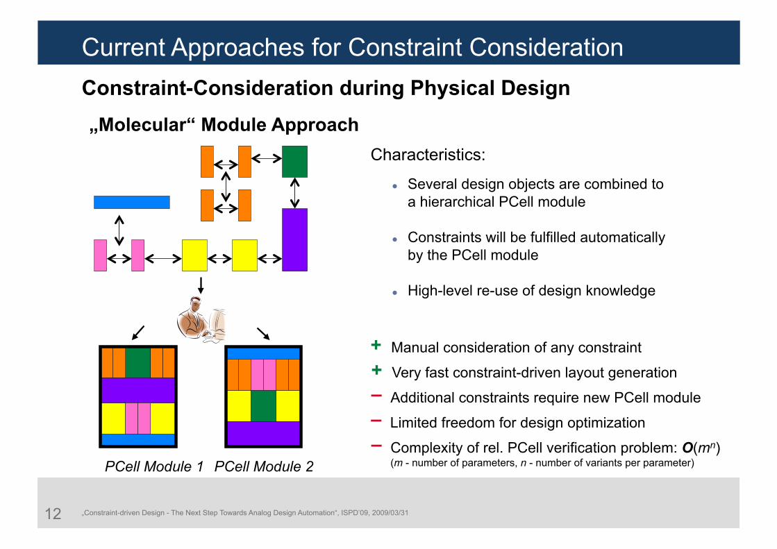
Current Approaches for Constraint Consideration Constraint-Consideration during Physical Design „Molecular“ Module Approach
PCell Module 1 PCell Module 2
Several design objects are combined to a hierarchical PCell module
Constraints will be fulfilled automatically by the PCell module
High-level re-use of design knowledge
Characteristics:
– Limited freedom for design optimization
– Additional constraints require new PCell module
+ Manual consideration of any constraint
– Complexity of rel. PCell verification problem: O(mn) (m - number of parameters, n - number of variants per parameter)
+ Very fast constraint-driven layout generation

„Constraint-driven Design - The Next Step Towards Analog Design Automation“, ISPD’09, 2009/03/31 13
Contents
The verification gap
Current approaches for constraint consideration
The constraint-driven design flow
Impact on design algorithms and design flow Open problems
Summary and conclusion

„Constraint-driven Design - The Next Step Towards Analog Design Automation“, ISPD’09, 2009/03/31 14
The Constraint-driven Design Flow Constraint Representation
Formalize constraints!
Define all constraints explicitly!
Account for design style!

„Constraint-driven Design - The Next Step Towards Analog Design Automation“, ISPD’09, 2009/03/31 15
T1
T3
T2 Pad
R(Pad->T1) < 1Ω?
R(Pad->T3) < 1Ω? R(Pad->T2) < 1Ω?
Simple and Complex Constraints
The Constraint-driven Design Flow
Simple constraint examples: VIR(Pad->T2) < 0.1 V Voltage class (Pad) = {50V, 80V}

„Constraint-driven Design - The Next Step Towards Analog Design Automation“, ISPD’09, 2009/03/31 16
T1
T3
T2 Pad
R(Pad->T1) < 1Ω?
R(Pad->T3) < 1Ω?
Complex constraint example (independent constraints): if ( net type == P&G ) then
[[Pad->T1], [Pad->T2], [Pad->T3]] must have star-shaped net topology && R(Pad->T1) < 1Ω && R(Pad->T2) < 1Ω && R(Pad->T3) < 1Ω !
R(Pad->T2) < 1Ω?
Simple and Complex Constraints
The Constraint-driven Design Flow

„Constraint-driven Design - The Next Step Towards Analog Design Automation“, ISPD’09, 2009/03/31 17
Design Data
Constraint Data
Constraint Management
Constraint Templates
Constraint Sensitivity
Analysis (CSA)
Constraint Verification
Constraint Transformation
Constraint Derivation
Transform. Models
Verification Rules
Circuit Design
Simulation
Floorplanning Device Generation
Placement
Routing
Compaction
Verification
Manufacturing
Test
Start
The Constraint-driven Design Flow

„Constraint-driven Design - The Next Step Towards Analog Design Automation“, ISPD’09, 2009/03/31 18
Constraint Management (Data Consistency)
DO2
DO1 C1
DOx - Design Object
Cy - Constraint
Today: Separate design and constraint databases
Design and Constraint Database
DO2
DO1
C1
V1.0
DO2
DO1
C1
V2.0
DO3 Future
Design Data
Constraint Data
– Difficult design and constraint data management (data consistency, data versioning)
The Constraint-driven Design Flow

„Constraint-driven Design - The Next Step Towards Analog Design Automation“, ISPD’09, 2009/03/31 19
Constraint Management (Propagation)
I1
I12 I11
I221
I22
I2
I222 I223
I21
T
Examples: - Floorplanning constraints - IR-drop constraints
Top-Down Propagation
C1
Top-Down and Bottom-Up Propagation
Examples: - ESD path definition - Net shielding
I1
I12 I11
I221
I22
I2
I222 I223
I21
T C3
Bottom-Up Propagation
Examples: - Placement constraints - Routing blockages
I1
I12 I11
I221
I22
I2
I222 I223
I21
T
C2
The Constraint-driven Design Flow

„Constraint-driven Design - The Next Step Towards Analog Design Automation“, ISPD’09, 2009/03/31 20
Constraint Derivation Methods
DOx - Design Object
Cy - Constraint
DO2
DO1
C1
?
?
Direct derivation rules and templates Example:
if ( differential pair ) then Assign matching constraint to transistor pair
Deduction processes Example:
Net N1 is connected to 40V IO pad && I1 is connected to net N1 ⇒ I1 is connected to 40V IO pad → Assign 40V design constraints to I1
Indirect method (transformation)
Expert knowledge
The Constraint-driven Design Flow

„Constraint-driven Design - The Next Step Towards Analog Design Automation“, ISPD’09, 2009/03/31 21
Constraint Transformation
Definition: Consistent and unambiguous transformation of high-level constraints into low-level constraints
Example: IR-Drop
1. Transformation of electrical constraints into circuit-specific constraints
Max. IR-Drop [V]
2. Transformation of circuit-specific constraints into layout-specific constraints Max. Resistance [Ohm]
3. Assignment of layout-specific constraints to (geometrical) design parameters
Wire length, -width layer …
The Constraint-driven Design Flow

„Constraint-driven Design - The Next Step Towards Analog Design Automation“, ISPD’09, 2009/03/31 22
Constraint Sensitivity Analysis (CSA)
Definition: Context-dependent sensitivity and gap determination of design parameters under consideration of one or more constraints
The Constraint-driven Design Flow
l h
dox
Isoline
Coupled constraints: VIR < VIR-max; RC < (RC)max; MTTF > MTTFmax
T0
x = f(T0-ΔT)?
w?
€
R = ρConductor ⋅l
w ⋅ h⋅ 1+ TK1 ⋅ T0 −ΔT( )( )
⋅+⋅⋅⋅⋅=
222.0
0 80.215.1oxox
r dh
dwlC εε
€
MTTF = A ⋅ w ⋅ hi
n
⋅ exp Ea
k ⋅ T0 −ΔT( )
€
VIR = i ⋅ R

„Constraint-driven Design - The Next Step Towards Analog Design Automation“, ISPD’09, 2009/03/31 23
Constraint Sensitivity Analysis (CSA)
The Constraint-driven Design Flow
VIR
w
ΔT = T1 = const.
ΔT < T1 = const.
ΔT > T1 = const.
VIR-max Sensitivity of w with respect to VIR
Sensitivity of w and ΔT with respect to VIR
Possible constraint violation !
w1 w2 w3

„Constraint-driven Design - The Next Step Towards Analog Design Automation“, ISPD’09, 2009/03/31 24
1. Constraints are not formalized
The voltage class of each well connected to a supply line should match
the voltage range occurring at the pad during operation!
Constraint Verification
4. Verify constraint fulfillment - Manual (4+n eyes verification) - Automatical verification
2 CV
2. Formalize constraints and verification task
For all power and ground pads: Get voltage class VPAD of pad
For all net terminals of the active net: Get voltage class VInst of owning instance
If VInst ≠ VPAD then Return ERROR Return SUCCESS
Constraints
3.2 Specify and implement verification routine(s)
3.1 Define verification requirements
Verification Rules 1
The Constraint-driven Design Flow

„Constraint-driven Design - The Next Step Towards Analog Design Automation“, ISPD’09, 2009/03/31 25
Constraint Verification (Example)
ESD-Verification
Netlist Layout
Circuit Verification
DRC / LVS
Symmetry Verification
IR-drop Verification
Reliability Verification
Property Verification … …
Circuit simulation
Sub-circuit recognition Layout polygon extraction
Terminal current retrieval Resistance calculation
EOS reliability calculation
Instance property retrieval Layout topology recognition
1
2
3
4
5
6
7
8
The Constraint-driven Design Flow
Combine capabilities of several tools to define and perform verification tasks !
1 2 3 1 4 5 1 1 4 7 8 5 4 6 8 5 4 3

„Constraint-driven Design - The Next Step Towards Analog Design Automation“, ISPD’09, 2009/03/31 26
Functionality:
Tool A
A1 A2 A3 An …
Functionality:
Tool B
B1 B2 B3 Bm …
CLP-based Logic Core &
Constraint Solver
TIKB
TIKA
CLP – Constraint Logic Programming TIK – Tool Integration Kit
Constraint data Design data Tool functionality
Constraint Templates
Constraint Sensitivity
Analysis (CSA)
Constraint Verification
Constraint Transformation
Constraint Derivation
Transform. Models
Verification Rules
Constraint-Engineering System (CES)
Constraint Solver
The Constraint-driven Design Flow
TIKX
TIKY

„Constraint-driven Design - The Next Step Towards Analog Design Automation“, ISPD’09, 2009/03/31 27
Constraint Rule File
Example: Check all pin-to-pin resistances RC,Pn in star-shaped nets: RC,Pn ≤ Rmax !
CES query for Rmax = 5 Ω: valStarRes(N, P, 5).
Result: List of all violating combinations of nets and terminals
Resistance-Extraction TIK
Topology- Extraction
TIK
Constraint
Layout-Extraction TIK
valStarRes(NetID, PinID, Rmax) :- R>Rmax, net(_, NetID), netLayout(NetID, L), topologyClass(_, L, star(C)), netPin(NetID, PinID), coordinate(PinID, P), resistance(_, L, C, P, R).
Constraint Verification
The Constraint-driven Design Flow

„Constraint-driven Design - The Next Step Towards Analog Design Automation“, ISPD’09, 2009/03/31 28
The verification gap
Current approaches for constraint consideration
The constraint-driven design flow
Impact on design algorithms and design flow Open problems
Summary and conclusion
Contents

„Constraint-driven Design - The Next Step Towards Analog Design Automation“, ISPD’09, 2009/03/31 29
Impact on Design Algorithms and Design Flow
Iterations
Time
Sequential Design Flow
Deg
ree
of D
esig
n Fr
eedo
m
Design Steps
Floo
rpla
nnin
g
Routing
Compaction
Phys
ical
Rea
lizat
ion
Compaction
Floorplanning
Continuous Design Flow [5]
Deg
ree
of D
esig
n Fr
eedo
m
Time
Phys
ical
Rea
lizat
ion
Future

„Constraint-driven Design - The Next Step Towards Analog Design Automation“, ISPD’09, 2009/03/31 30
High-Level Design Algorithms
Impact on Design Algorithms and Design Flow
Design Problem
Algorithm 2 Algorithm 3 Algorithm 1 Algorithm n … IFC IFC IFC IFC
High-Level Design Algorithm
Design and Constraint Database
Strategy A: 1. Placement Alg.1 2. Glob. Routing Alg.2 3. Det. Routing Alg.6
Strategy B: 1. Route Planning Alg.4 2. Placement Alg.9 3. Det. Routing Alg.6
„Constraint-driven Design - The Next Step Towards Analog Design Automation“, ISPD’09, 2009/03/31 31
Contents
The verification gap
Current approaches for constraint consideration
The constraint-driven design flow
Impact on design algorithms and design flow Open problems
Summary and conclusion

„Constraint-driven Design - The Next Step Towards Analog Design Automation“, ISPD’09, 2009/03/31 32
Open Problems (Long Term)
Constraint solver: Consideration of constraints with statistical boundaries is required
Constraint methods: Scalability of constraint sensitivity analysis (CSA) must be improved Approaches for automatic constraint rule optimization should be developed
High-level design algorithms: Improvement of concepts for abstraction of design and verification algorithms Development of strategies for high-level design task partitioning (with CSA)

„Constraint-driven Design - The Next Step Towards Analog Design Automation“, ISPD’09, 2009/03/31 33
Summary and Conclusion
Presentation covered (1) today’s verification gap, (2) current and future approaches for constraint-driven design and (3) open problems
Constraint-driven design is a major and a necessary step towards a fully-automated analog design synthesis
Constraint verification reduces the existing verification gap in A/MS designs
The comprehensive and automatic constraint consideration is a potentially disruptive technology with a very strong impact on the design process!
Constraint-driven X-design interdisciplinary field with a tremendous potential and many challenging problems

„Constraint-driven Design - The Next Step Towards Analog Design Automation“, ISPD’09, 2009/03/31 34
Thank You!

„Constraint-driven Design - The Next Step Towards Analog Design Automation“, ISPD’09, 2009/03/31 35
Bibliography
[1] J. Jaffar et al.: “The CLP(R) language and system: an overview” in Proc. Compcon Spring 1991, Digest of Papers, pp. 376-381, 1991.
[2] E. Malavasi, E. Charbon et al.: “Automation of IC Layout with Analog Constraints”, in IEEE Trans. on CAD of Integrated Circuits, Vol. 15, No. 8, 1996.
[3] E. Malavasi, E. Charbon: “Constraint Transformation for IC Physical Design”, in IEEE Trans. on Semiconductor Manufacturing, Vol. 12, No. 4, 1999.
[4] J. Freuer, G. Jerke, J. Gerlach, W. Nebel: “On the Verification of High-Order Constraint Compliance in IC Design”, in Proc. Design, Automation and Test in Europe, DATE '08, pp. 26 – 31, 2008.
[5] Scheible, Jürgen: “Constraint-driven Design – Eine Wegskizze zum Designflow der nächsten Generation”, in Proc. Beiträge der 10. GMM/ITG-Fachtagung, Analog’08, Siegen, Germany, 2008.
[6] G.Jerke, J. Lienig: “Constraint-Driven Design – The Next Step Towards Analog Design Automation”, in Proc. International Symposium on Physical Design, ISPD’09, 2009.
[7] Sakurai T., Tamaru, K.: “Simple Formulas for 2D and 3D capacitances”, in IEEE Trans. Electron. Dev., Vol. ED30, No.2, pp. 183-185, 1983.