contribution to digital pfc controllers in hid lamps
TRANSCRIPT

1
Contribution to digital PFC controllers in HID lamps electronic ballast applications
F. Javier Diaz, Member, IEEE, Victor M. Lopez, Student Member, IEEE, Francisco J. Azcondo, Senior Member, IEEE, C. Brañas, Member, IEEE, R. Casanueva, Member,
IEEE.
University of Cantabria
Electronics Technology, Systems and Automation Engineering Department
Ave. de los Castros s/n 39005 Santander (Cantabria), SPAIN
{ diazrf, lopezvm, azcondof, branasc, casanuer}@unican.es
Abstract— Utility voltage fluctuations not compensated by the low frequency voltage loop of the
power factor correction (PFC) stage cause a perceptible variation in the light emitted by lamps,
unpleasant for the human eye and known as flicker effect. A novel extension of the digital control
for PFC stages analyzes the input voltage, detects the fluctuations in the range of human flicker
sensitivity and modifies the PFC output voltage controller to avoid their propagation to the dc bus.
The purpose of the controller is to make the PFC compatible with any second stage lamp driver,
assuring the mitigation of the lamp light variation caused by utility disturbances in consistency
with the human eye perception. The controller is implemented in a Field Programmable Gate
Array (FPGA). A constant lamp luminance is achieved with this digital controller with no
dependence of the next ballast stage.
1 Introduction
Nowadays, the power conversion systems leverage the digital control capabilities to introduce more
flexible power conversion strategies and increase the reliability. A detailed analysis of the benefits of
using digital control-based controllers in power electronics and drive applications is found in [1]-[8].
Designers have the choice between two main families of digital device technologies for fast prototyping.
The first family [1]-[4] is associated to microcontrollers and Digital Signal Processor (DSP) controllers.
These components integrate a performing microprocessor core along with several peripherals. The

2
alternative family is the Field Programmable Gate Arrays (FPGAs) technology [9], [10]. These devices
consist of predesigned elementary cells and interconnections that are fully programmable by the end user.
In DC/DC conversion, it is common that digital controllers pay close attention on the voltage regulation
with improved dynamic performance under input voltage and load transients [11], [12].
Key properties of High Intensity Discharge (HID) lamps include higher energy efficiency, compact size,
good colour rendering, whiter light (higher colour temperature), and longer lifetime [13]-[19]. Typical
applications range from car headlamps, greenhouse lighting, interior lighting, industrial sector and urban
lighting applications. Since the urban lighting consumption represents a non-negligible part of the total
energy amount consumed on Earth, improvements of the supply, efficiency and light quality are
investigated. Digital control is a key technology to provide higher performance [14]-[16] to the ballast
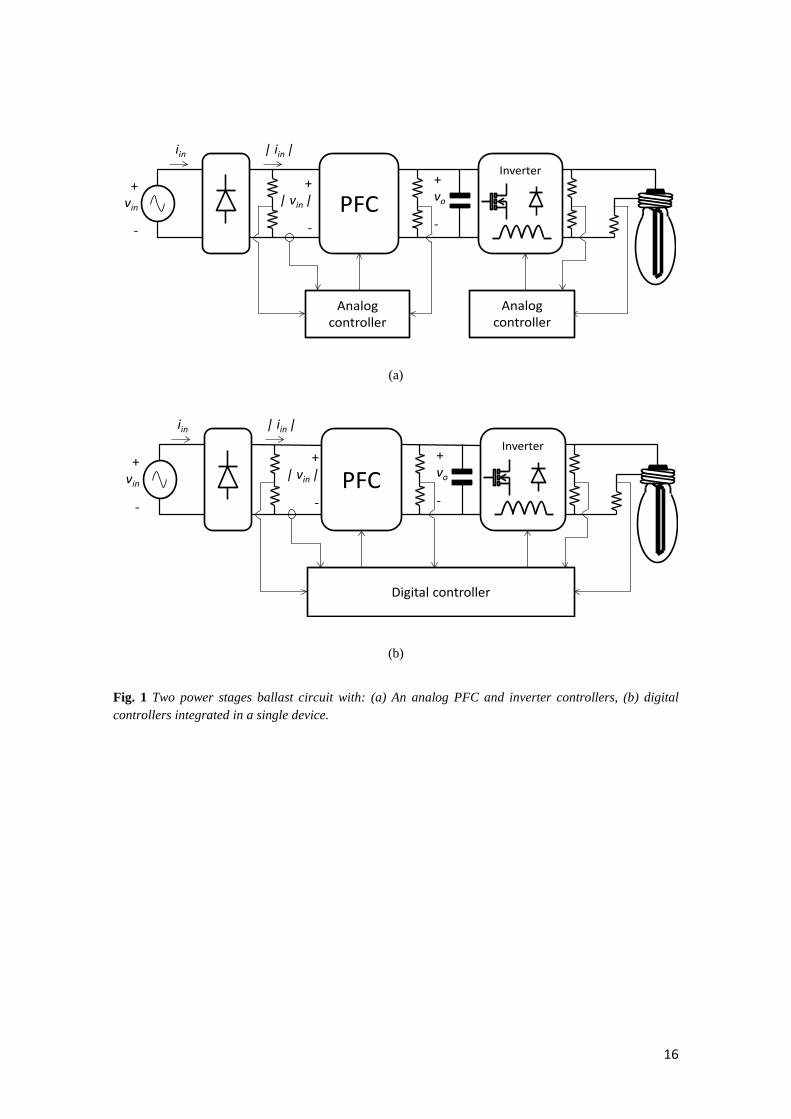
system. In Fig. 1.a, a typical two – stage electronic ballast solution is shown including a power factor
correction (PFC) [20] and an inverter. On the other hand, the same system is depicted in Fig. 1.b with a
digital controller.
Light emitted by HID lamps is very sensitive to voltage supply fluctuations, producing an effect on the
human visual perception, known as flicker [21]-[26]. Flicker is a very uncomfortable effect, which would
cause a lot of human physiological effects as it is indicated in [24] and [25]; so it is addressed as a safety
and health issue at work. These fluctuations can be caused by the connection and disconnection of
important loads (high-power motors, PFC bank capacitors, etc…), compressors, resistive welding
machines or arc furnaces. Flicker frequency can be perceived by the eye-brain set, when it is within a
range of frequency that extends from 0.5 to 25 Hz [23]; and the maximum flicker perception occurs at
around 10 Hz [26].
In two-stage electronic ballast, where the inverter may operate in open loop, the PFC outer loop and its
output bulk capacitor, C, are the elements that attenuate the propagation of the utility voltage fluctuation
to the dc bus and then contribute to reduce the light variation in HID lamps. This work presents an
extension of the PFC control technique presented in [11] and [12] specifically adapted to prevent the lamp
flickering. This extension can also be applied to digital PFC controllers that use input current sensor to
improve the performance in lamp driver applications. The present work has precedents in the conference
papers [23], [27], [28]. The update over those works includes a more detailed presentation of the signals
acquisition circuit, identification of the conventional voltage regulator, the additional regulator to prevent

3
the lamp flickering and the hardware connection to achieve a consistent operation. A novel algorithm to
detect the fluctuations over the nominal incoming voltage level and select the condition to activate the
additional controller to prevent the lamp flickering is presented in this work. Also, experimental results
have been updated including frequency response oscillograms. The amplitude of the low frequency PFC
output ripple voltage caused by the fluctuation of the utility voltage is attenuated by increasing the PFC
output capacitance. This technique can also be applied to attenuate the propagation of the utility
disturbances that cause flickering, but a larger capacitor increases the volume and size of the converter
and as long as the electrolytic capacitor cannot be replaced by other technology, the circuit lifetime is
penalized [29]-[32]. An alternative is the implementation of a wide bandwidth controller in the inverter
stage [19]. In [33], two control algorithms are presented for Distribution STATic synchronous
COMpensator (DSTATCOM) to mitigate voltage fluctuation caused by electric arc furnace loads.
Representative works on utility voltage detections are [34] and [28], where a technique to monitor voltage
fluctuations in the power system with a least-squares-Kalman optimization technique for fundamental
frequency voltage phasor estimation and an input instantaneous voltage detection algorithm, under ideal
utility mains, are presented respectively.
The proposed digital compensation of the voltage fluctuation does not modify the original PFC output
voltage controller if low frequency fluctuations of the input voltage are not detected. When these
fluctuations appear, the proposed controller changes the voltage loop dynamic response to minimize the
dc voltage ripple at the fluctuation frequency assuring a constant light luminance in the lamp and
avoiding the optical flicker perception. No extra cost and no extra analog components are introduced
whenever the FPGA can host the small additional digital block. To clearly show the performance
achieved, a practical application with a 150 W HPS (High Pressure Sodium) lamp supplied by an open
loop resonant inverter as second stage (Fig. 1) is presented.
The objectives of this paper are: 1) to develop a universal voltage fluctuation detection method that fits
the standard definition human perception range. 2) To use the lowest PFC output capacitance, C, by
extending the capabilities of the digital output voltage loop, and 3) to minimize the flicker perception for
the human eye caused by the utility disturbances.

4
For further hardware simplification of the lamp driver oriented PFC controller, the implementation has
been carried out as an extension of the digital control technique presented in [11] and [12], which requires
neither current sensor nor high speed analog-to-digital converter.
The paper is organized in five sections. After introduction, the proposed digital PFC controller is
presented in Section 2; with a first subsection about the input current control and a second subsection with
the digital outer voltage loop. In Section 3, the voltage fluctuations detection algorithm is shown. In
Section 4, experimental results with a HID lamp are presented, finalizing with conclusions.
2 The digital PFC controller
A. Inner current loop
Some advantages that motivate the use of digital control in PFC stages include: reduction of discrete
components, ease of controller implementation and extension of its performance limits, reduction of size
and reduction of sensitivity to parameter tolerances, [35], [36], [37].
The principle of operation of the digital current control to achieve power factor correction used in this
work, and depicted in Fig. 2, has been presented in [11], [12], [35], [36] where an input current (iin)
estimator removes the need for current A/D conversion and input and output voltages are measured using
the analog-to-digital converters (ADCs) represented in green in Fig. 2. Avoiding the current measurement
means a step-forward with respect to analog controllers, which also helps to increase efficiency and
reduce the total cost and complexity. Input and output voltages measurements (vinADC and voADC) are used
to estimate the input current digitally (iinreb). As ADCs, first order ad-hoc sigma-delta converter with a
low quantity of analog components (an RC filter and a comparator) [11] is used in the output voltage
measurement. A commercial ADC is used for the input voltage A/D conversion. The analog circuitry
used to substitute the current sensing circuit is presented in blue.
Drain-to-source MOSFET voltage is adapted as digital input signal (vds) in order to measure and
compensate drive signal’s delays. With this digital controller, a sinusoidal current waveshape is obtained,
independently of the voltage or power conditions.
B. Outer voltage loop

5
In steady-state operation, the PFC output voltage loop has a low bandwidth (up to 10 Hz) so not to
interfere with the inner loop that keeps the current shape proportional to the input voltage to comply with
the IEC 61000-3-2 for class C equipment [20].
The action of the low bandwidth cannot reject the low-frequency fluctuations and they are propagated
through the PFC and inverter stages, perturbing the lamp current and voltage, as is depicted in Fig. 3.a.
The current fluctuation causes the lamp light variation, and then the flicker effect.
In order to attenuate this flicker effect, the capacitance of the output bulk capacitor (C shown in Fig. 2) in
the PFC stage could be chosen higher than the calculated with (1), which determines the capacitance
needed to limit the amplitude of the voltage ripple at twice the line frequency, ∆Vo, below a given value
min,ooo VVV −=∆ , supplying a power rate P, where Vo and Vo,min are the average and minimum output
voltage in steady state respectively, and Tu is the utility period.
2min,
2oo
u
VVPTC−
> (1)
This solution needs electrolytic capacitors which limit the useful life of the ballast system.
Figure 3.b shows the target behaviour of the proposed control. During steady state, the output voltage
loop has a low bandwidth and a current shape proportional to the input voltage and also has an extended
bandwidth loop in the utility voltage fluctuations situation with current distortion. Standard IEC 61000-3-
2 class C [20] is not applied in presence of these utility transients. A constant PFC stage output voltage
(vo) is achieved despite input voltage low frequency fluctuations. With this, constant lamp current (ilamp),
and then constant lamp light luminance are also achieved.
In previous work [27], the design of a small-signal model of the NLC (Nonlinear-Carrier) controlled
boost rectifier and the analysis to obtain the control-to-output transfer function G(s) was presented
following [39]. The output voltage control loop has been designed using the G(s), whose expression is
( ) ( )( )
31
13
2,
RCsrR
VV
sVsVsG
so
RMSin
m
o
+
== , (2)
6
where rs is the virtual current sensor resistor, R is the load and C the output capacitor as is shown in
Fig. 4, while vm is the NLC control voltage. Details of the sequence to obtain (2) are given in the
Appendix.
A digital voltage loop is shown in Fig. 4.a, where a low bandwidth compensator, Css(z) is implemented to
assure that the output voltage that supplies the second stage follows the reference (voref). The block
diagram of the proposed digital controller is presented in Fig. 4.b, where the block “Current loop”
represents the NLC controller presented in Fig. 2. When utility disturbances appear, an utility voltage
fluctuations detector, presented in Section III, activates the compensator Cfluc(z) in order to extend the
bandwidth of the PFC outer loop, avoiding their propagation to the lamp at the expense of increasing the
utility current distortion. With this capability, a low C value can be utilized. The design of the controllers
was presented in previous works [27-28], using the following sequence. 1) A proportional integral (PI)
action is selected for both controllers as the right option to obtain high loop gain at very low frequency
and around 90º phase lag at the cross-over frequency. At least 52º phase margin, pm, is desired to prevent
transient oscillations. 2) Css(z) is designed to set the loop gain crossover frequency, fc, around 1Hz, thus
avoiding line current distortion in steady-state [3]. 3) Cfluc(z) is designed to set, fc, around 100Hz, a decade
above 10 Hz, which determines the upper flicker detection limit of the human eye. 4) To simplify the
digital implementation in the FPGA, the coefficients of both controllers are approximated to powers of 2,
verifying the resulting fc and pm with Matlab- Sisotool ®. Table I shows the plant and the designed
controllers in the z-domain.
3 Input voltage fluctuations detection algorithm
The utility peak voltage value (vin,peak) is obtained, cycle by cycle, with a digital peak detector of the
digital input voltage (vinADC). With this value, the steady-state utility peak voltage and three different
voltage levels are defined as is shown in Fig. 5.a. The algorithm defines the non-fluctuation band (called
“In” in Fig. 5.a), with the steady-state utility peak voltage, vin,peak ±2%.
When the utility peak voltage is found outside this band, i.e. “Above” or “Below” in Fig. 5.a, the
algorithm determines whether there is a fluctuation in the most sensitive frequency range of the human
eye, between 0.5 to 25 Hz. It is assumed that fluctuation component of the utility voltage is approximately
a symmetric function, i.e. it can be reflected around a specific time location. Consequently, if the
fluctuation period is Tf, every Tf/2 the utility voltage envelope crosses the limits of the voltage band.

7
When the first change in the peak value is detected, the algorithm measures the time (Ti) throughout the
peak voltages are maintained in each band. If Ti lasts between 0.02 s and 1 s (half period of a 25 and 0.5
Hz fluctuation, respectively), it is considered that there is a utility voltage fluctuation. Therefore, precise
fluctuation frequency is only measured if it is in the 0.5 to 25 Hz range, where it produces an unpleasant
optical flicker perception.
The input voltage fluctuation detection algorithm flowchart is shown in Fig. 5.b. The signal
“Fluctuation” is set to “1” under flicker situation, and therefore the time during the wide bandwidth
voltage loop has to be applied (Twide-loop) is determined.
4 Experimental results
Laboratory experiments that illustrate the performance of the digital controller have been carried out with
electronic ballast for a 150 W HPS lamp (LUCALOX). A boost converter has been used as PFC stage.
Values of the components are: L = 3.2 mH, Vin = 230 V (50 Hz), fsw = 73 kHz, Vo = 420 V and Po= 150 W.
The output bulk capacitance is 68 μF.
A LCC half-bridge resonant inverter (RI) is used as second stage. It provides the required ballast action at
reduced cost and behaves as an input voltage-dependent power source. Since the compensation of the
utility fluctuation is carried out by the PFC stage, it can be connected to other type of second stages and
light sources [14], [15], [28] and [38].
The LCC resonant circuit is designed to have zero resonant current phase lag at the end of the lamp
lifetime, and it works in a frequency window free of acoustic resonance, which is a valid solution for
150 W HPS lamps [14]. This inverter operates in open loop, so it is a system without capability for
compensation of input voltage disturbances, being a good example to illustrate the performance of the
proposed digital controller. ZVS is guaranteed in the resonant inverter along with a minimum reactive
component in the resonant tank considering the whole life span of the lamp. Using the design sequence
described in [14], the RI design is defined by Zp = Rlamp/Qp = 170 Ω, Lr = 115 µH, Cp = 5.7 nF and
Cs = 330 nF.
For laboratory test purposes, the digital control circuit is implemented in a Xilinx Spartan 3 family
XC3s200e FPGA. In order to measure the behaviour of the system with the proposed digital control, an
APDS-9007 ambient light photo sensor is used. This photo sensor has a spectral response close to the

8
standard photopic observer. The photo sensor is placed in front of the lamp to get an output voltage
proportional to the brightness of the lamp light, according to what human eye perceives). An Agilent
6813B AC programmable power source is used to supply the HID lamp power supply.
Figure 6.a shows the PFC stage input current (iin) and the input voltage (vin) waveforms in steady-state
situation. Despite not measuring the input current, power factor correction is successfully achieved. The
measured power factor was 0.991 with 168 W input power (Pin).
In Fig. 6.c, the Fast Fourier Transform (FFT) on the input current in comparison with the IEC 61000-3-2
class-C limits shows that all current harmonics are below the limits recommended by the standard.
Figure 6.b shows the PFC stage input current (iin) and the input voltage (vin) waveforms during utility
fluctuation with the wide bandwidth outer loop. In this case, the power factor is 0.91. The input current is
distorted because of the faster dynamic response. Figure 6.d, shows that the harmonic content of the input
current does not comply with the IEC 61000-3-2 class C limits, but in the utility fluctuation case the
mentioned standard does not apply [20].
The phase margin and the crossover frequency are 73º and 0.61 Hz for the reduced bandwidth voltage
loop (Figs. 6.a and 6.c), and 78.8º and 149 Hz for the wide bandwidth loop (Figs. 6.b and 6.d). Output
voltage reference is the same for both controllers; in this case 420 Vdc. Fig. 7 shows the Bode diagrams of
the extended bandwidth (blue) and the reduced bandwidth (green) outer loops.
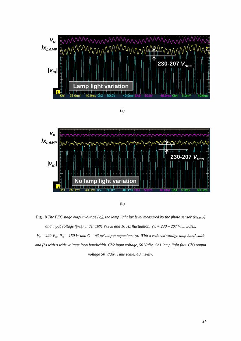
The PFC stage dc output voltage (vo), the lamp light lux level measured by the photo sensor (lxLAMP) and
the input voltage (vin) to the PFC stage under a 10% fluctuation (ΔV) in the input voltage (programmed in
the AC power source) are shown in Fig. 8.a when the PFC uses the slow PFC outer loop, and in Fig. 8.b
when the PFC uses the fast PFC outer loop to compensate the fluctuation.
Fluctuation frequency has been set close to the maximum level of human eye flicker perception, i.e.
10 Hz. Figure 8 shows the same input voltage and the differences on lxLAMP and vo waveforms between
applying or not the extended bandwidth outer loop. In Fig. 8.a, the lxLAMP signal has a fluctuation of
10 Hz (added to the output voltage 100 Hz fluctuation, imperceptible by the human eye). On the other
hand, in Fig. 8.b this fluctuation is highly attenuated, because the wide bandwidth voltage loop is applied.
In this case, lamp light variation and flicker perception disappear.

9
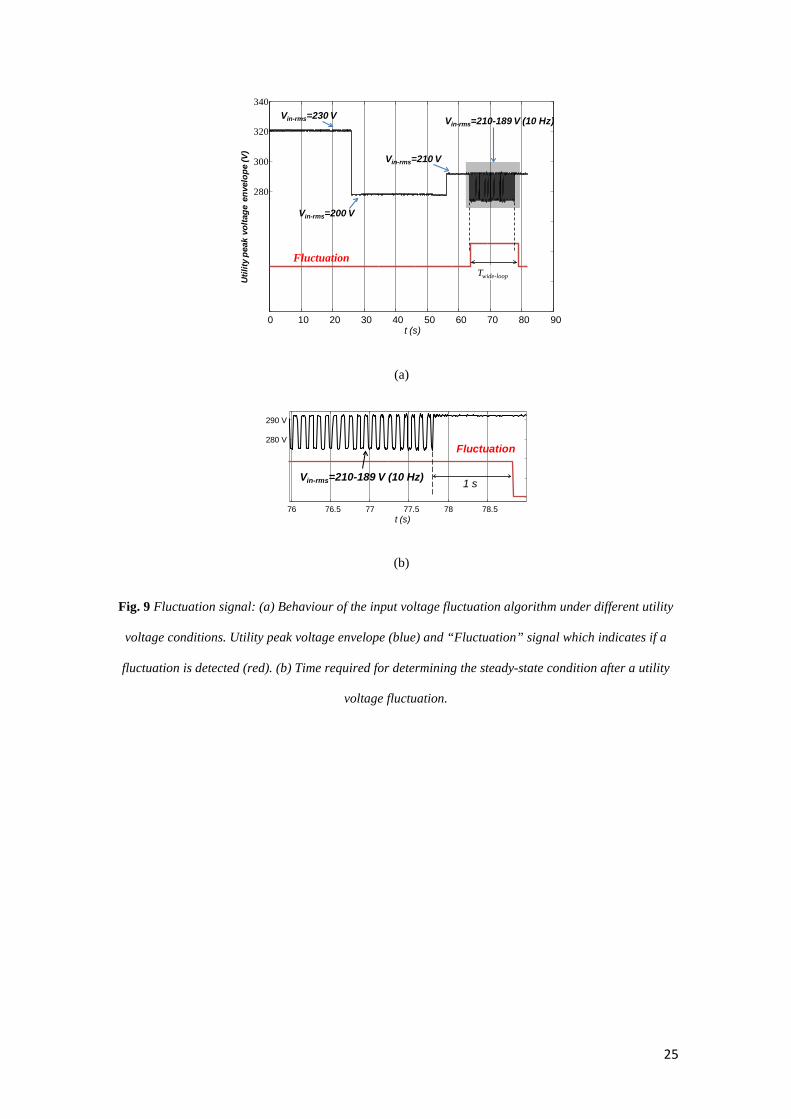
Figure 9 shows the behaviour of the input voltage fluctuation detection algorithm. Figure 9.a displays the
signal “Fluctuation” under different utility voltage conditions. At first, a 230 Vrms (325 V peak) utility
voltage is applied. After 27 seconds, a step down of 30 Vrms is applied; and then, after 30 seconds, 210
Vrms (297 V peak) input voltage is applied. In this situation, a 10 % and 10 Hz fluctuation is imposed (210
– 189 Vrms).
The algorithm determines the steady-state peak voltage and defines the ±2% “In” band. When the
fluctuation is detected, the signal “Fluctuacion” turns to “1”. The extended bandwidth voltage loop is
applied during the time Twide-loop. Figure 9.b demonstrates the result of the algorithm behaviour at the end
of the fluctuation. It can be seen that a 1 second period is necessary to determine that the fluctuation has
finished.
5 Conclusions
A digital controller for power factor correction circuits applied to HID lamp electronic ballast has been
proposed. This controller, implemented in a FPGA, makes the utility current to meet the IEC 61000-3-2
class C limits in steady-state and rejects input voltage fluctuations to avoid lamp flicker [20].
The proposed controller extension, specific for ballast application, is applied to a PFC controller which
requires no current sensor to shape the input current. The input current of the ballast system is estimated
from the input and output voltages of the PFC stage. Avoiding the current measurement is a significant
advantage with respect to other controllers because it eliminates a hot spot in the circuit and improves the
noise immunity of the control circuit.
A voltage fluctuations detection algorithm is used to avoid the propagation of the fluctuations to the lamp.
The algorithm measures the steady-state utility peak voltage and detects low frequency voltage
fluctuations in the most sensitive frequency range of the human eye. Depending on the detected
disturbances, the digital controller modifies the voltage-loop speed of the PFC-stage, reducing the light
flicker emission within the frequency band of human perception of the flickering. The proposed digital
controller is a valid solution even though the higher bandwidth (149 Hz) voltage loop distorts the input
current. This is compatible with the IEC 61000-3-2 standard because the essay to define the standard
compliance is defined in steady-state and the utility voltage level fluctuation implies a transient state.
10
A two stage ballast system (Boost PFC + Resonant Inverter) that supplies a 150 W HPS lamp has been
subjected to low frequency utility fluctuations. These fluctuations have been programmed with an AC
power electronic source in order to produce a variation on the light emitted close to the maximum level of
human eye flicker perception, emulating an industrial environment under grid disturbances.
A constant light luminance in the lamp is achieved despite frequency utility mains fluctuations and
without extra components external the digital circuit. Moreover, the size of the PFC output capacitor is
reduced, decreasing the volume and cost, and increasing the lifetime of the converter.
Appendix
The implemented non-linear controller (inner current control) defines d by comparing (iL(t0)+iL(t))/2
multiplied by a real or artificial sensor resistance rs with the carrier signal vm(1-(t-t0)/T) in each switching
period. The variable vm is the control variable that will be provided by the outer voltage loop. The
function iL(t) represents the current through the inductor in the time domain and iL(t0) is the current
through the inductor at the beginning of a given switching period. Therefore, the condition
( ) ( )
−−=
+T
ttvrtitims
LL 00 12
(a.1)
results in
( ) ( )
−=
++TdTvrdTtiti
msLL 12
00 (a.2)
Assuming that the computed value is the current trough the inductor averaged over the switching period,
T, <iL>T, the previous expression can also be rewritten for each switching period as
( )dvri msTL −= 1 (a.3)
Assuming also high switching frequency in comparison with the dynamics of the averaged variables this
equation can be defined in the time-domain
( )To
TinmsTL v
vtvri = (a.4)
11
The quasi-static approximation, which assumes ac line variations much slower than the converter
dynamics, reveals that the non-linear controller shapes the current to be proportional to the input voltage
when the ripple of the output voltage is low, as desired for the power factor correction application,
justifying the proposed non-linear controller.
Perturbing the control variable mv around a given operation point defined by the DC output voltage, Vo
inductor current, IL, and control signal, Vm values with D
VV ino −=
1,
( )DRVI o
L −=
1 and
( )DVrI msL −= 1 , the following transfer function is obtained
( ) ( ) ( ) 2os
inmo
os
inmL Vr
VVsVVr
VsVsI −= (a.5)
From <iL>T in (a.4), the averaged current through the RC load, i.e. the load resistor R and the output filter
capacitor C shown in Fig. 4.b, in the switching period, <iRC>T, is obtained as,
( )To
TinTLTLTRC v
vidii =−= 1 (a.6)
Assuming sinusoidal input voltage and using the notationmax,TLi ,
max,Tinv , for the averaged input
current and voltage at the ac utility angle p/2, the output voltage results from averaging the converter
operation over half line period (Tu/2), and the transfer function that defines the plant is the response of the
output voltage of the averaged over the utility period model, Tuov , to perturbations of vm.
The quasi-static approximation with low output voltage ripple assumesTuoTo vv = . Therefore, the
current through the load averaged over the utility period is calculated as
( ) ( )Tuo
Tu
Tuo
TinTLt
t To
TinTL
TuRC vp
vvi
tdtv
vii === ∫
+
−2
sin1 max,max,2
2
2max,max, ωωp
pω
pω
(a.7)
From this result defined in the time-domain, a small-signal expression, in this case defined in the Laplace
domain can be obtained, where the upper case notation without the Laplace complex argument (s) is used

12
for the DC values. Therefore, IRC(s), IL,max(s), Vin,max(s) and Vo(s) correspond to the small-signal
perturbation of <iRC>Tu, <vin>T,max and <vo>Tu respectively Vin,max, IL,max, Vo and R define the DC
operation point
( ) ( ) ( ) ( )R
sVV
IsV
VV
sIsI oo
Lin
o
inLRC
122
max,max,
max,max, −+= (a.8)
The plant to be controlled by the outer loop is obtained by introducing (a.5) into (a.8), and using Vm(s) as
the only input, i.e. Vin,max(s) = 0.
( ) ( ) ( )R
sVVr
VsVsI o
os
inmRC
22 2
2max, −= (a.9)
( ) ( )sRCRsIsV RCo +
=1
(a.10)
The use of a resistance as the small-signal load is justified because here it is considered the case of the
next section, i.e. the inverter, operating in open loop and the range of the small-signal perturbation
frequency is low. A closed loop controlled inverter would modify its small-signal behaviour as a load.
( ) ( )( )
31
13
2,
RCsrR
VV
sVsVsG
so
RMSin
m
o
+
== (a.11)
Acknowledgments
This work is sponsored by the Spanish Ministry of Science and the EU through the project CICYT-
FEDER-TEC2011-23612: “Power conversion with new digital control techniques and soft-saturation
magnetic cores”.
References
[1] E. Monmasson, L. Idkhajine, M.N. Cirstea, I. Bahri, A. Tisan and M.W. Naouar, "FPGAs in Industrial Control Applications," IEEE Trans. Ind. Informat., vol. 7, no. 2, May 2011, pp. 224-243.
[2] E. Monmasson and M. Cirstea, “Guest editorial special section on field programmable gate arrays (FPGAs) used in industrial control systems,” IEEE Trans. Ind. Electron., vol. 54, no. 4, Aug. 2007, pp. 1807–1809.

13
[3] D. Maksimovic, R. Zane and R. Erickson, "Impact of digital control in power electronics," Proc. IEEE International Symposium on Power Semiconductor Devices and ICs (ISPSD 2004), 24-27 May 2004, pp. 13- 22.
[4] M. P. Kazmierkowski, M. Jasinski, and G. Wrona, “DSP-Based Control of Grid-Connected Power Converters Operating Under Grid Distortions,” IEEE Trans. Ind. Informat., vol. 7, no. 2, May 2011, pp. 204 -211.
[5] L. Idkhajine, A. Prata, E. Monmasson, K. Bouallaga and M. W. Naouar, "System on Chip controller for electrical actuator," Proc. IEEE International Symposium on Industrial Electronics ( ISIE 2008), June 30 2008-July 2 2008, pp. 2481-2486.
[6] J. M. Guerrero, F. Blaabjerg, T. Zhelev, K. Hemmes, E. Monmasson, S. Jemei, M.P. Comech, R. Granadino and J.I. Frau, "Distributed Generation: Toward a New Energy Paradigm," IEEE Ind. Electron. Mag., vol. 4, no. 1, March 2010, pp. 52-64.
[7] A. Malinowski and Hao Yu, "Comparison of Embedded System Design for Industrial Applications," IEEE Trans. Ind. Informat., vol. 7, no. 2, May 2011, pp. 244-254.
[8] Man Ho Kim, Suk Lee and Kyung Chang Lee, "Kalman Predictive Redundancy System for Fault Tolerance of Safety-Critical Systems," IEEE Trans. Ind. Informat., vol. 6, no. 1, Feb. 2010, pp. 46-53.
[9] E. Monmasson, L. Idkhajine and M.W. Naouar , "FPGA-based Controllers," IEEE Ind. Electron. Mag., vol. 5, no. 1, March 2011, pp. 14-26.
[10] J. J. Rodriguez-Andina, M. J. Moure and M. D. Valdes, "Features, Design Tools, and Application Domains of FPGAs," IEEE Trans. Ind. Electron., vol. 54, no. 4, Aug. 2007, pp. 1810-1823.
[11] F. J. Azcondo, A. de Castro, V. M. Lopez and O. Garcia, “Power factor correction without current sensor based on digital current rebuilding”, IEEE Trans. Power Electron., vol. 25, no. 6, Jun 2010, pp. 1527-1536.
[12] V. M. Lopez, F. J. Azcondo, F. J. Diaz and A. de Castro, “Autotuning digital controller for current sensorless power factor corrector stage in continuous conduction mode”, Proc. IEEE Workshop on Control and Modeling for Power Electronics (COMPEL 2010), University of Colorado, Boulder, Colorado, USA, June 2010.
[13] J. de Groot and J. Van. Vliet, The High-Pressure Sodium Lamp. Philips Technical Library, Macmillan Education, 1986.
[14] F. J. Azcondo, F. J. Díaz, R. Casanueva and C. Brañas, “Microcontroller Power Mode Stabilized Power Factor Correction Stage for High Intensity Discharge Lamp Electronic Ballast,” IEEE Trans. Power Electron., Part Special Section on Lighting Applications, vol. 22, no. 3, May 2007, pp. 845-853.
[15] F. J. Diaz, F. J. Azcondo, R. Casanueva, C. Branas, and R. Zane, “Digital control of a Low-Frequency Square-Wave electronic ballast with Resonant Ignition,” IEEE Trans. Ind. Electron., vol. 55, no. 9, Sep. 2008, pp. 3180-3191.
[16] B. Divakar, K. Cheng, D. Wang, D. Ping, and K. Kwok, “Implementation of a Voltage Multiplier Integrated HID Ballast Circuit With Dimming Control for Automotive Application,” IEEE Trans. Ind. Electron., vol. 56, no. 7, Jul. 2009, pp. 2479-2492.
[17] R. Orletti, M. Co, D. Simonetti, and J. de Freitas Vieira, “HID Lamp Electronic Ballast With Reduced Component Number,” IEEE Trans. Ind. Electron., vol. 56, no. 3, Mar. 2009, pp. 718-725.
[18] R. Sanchez, N. Vazquez, C. Hernandez, E. Rodriguez, S. Pinto, and M. Juarez, “Electric Dynamic Modeling of HID Lamps for Electronic Ballast Design,” IEEE Trans. Ind. Electron., vol. 57, no. 5, May 2010, pp. 1655-1662.

14
[19] C. Brañas, F. J. Azcondo and R. Zane, “Power-mode control of multiphase resonant electronic ballast,” IEEE Trans. Ind. Electron., vol. 59, no. 4, April 2012, pp. 1770-1778.
[20] Standards on Electromagnetic Compatibility (EMC), Part 3, Section 2: Limits for Harmonic Current Emissions, IEC 61000-3-2 Edition 2:2000, Jan. 2004.
[21] CENELEC, EN 50160. Voltage Characteristics of Electricity Supplied by Public Distribution Systems. 2001.
[22] R. Cai, J. F. G. Cobben, J. M. A. Myrzik, J. H. Blom and W. L. Kling, "Flicker responses of different lamp types," IET Generation, Transmission & Distribution, vol. 3, no. 9, Sept. 2009, pp. 816-824.
[23] F. J. Azcondo, M. Mañana, A. Ortiz, F. J. Díaz, C. Brañas, C. Renedo, S. Pérez, F. Delgado and R. Casanueva, "Voltage Fluctuations in Lamps and Ballasts," IEEE Ind. Appl. Mag., vol. 17, no. 5, Sept.-Oct. 2011, pp. 45-52.
[24] A.E. Emanuel, and L. Peretto, “A simple lamp-eye-brain model for flicker observation,” IEEE Trans. Power Del., vol. 19, no. 3, July 2004, pp. 1308-1313.
[25] L. Peretto, L. Rovati, G. Salvatori, R. Tinarelli and A. E. Emanuel, "Investigation on the Response of the Human Eye to the Light Flicker Produced by Different Lamps," Proc. IEEE Instrumentation and Measurement Technology Conference (IMTC 2006), April 2006, pp. 37-42.
[26] IEC, IEC 61000-4-15. Electromagnetic Compatibility (EMC) - Part 4: Testing and Measurement Techniques - Section 15: Flickermeter - Functional and Design Specifications. 2003.
[27] F. J. Diaz, V. M Lopez, F. J. Azcondo, “New specification for the PFC controller in HID lamps electronic ballast”, Proc. IEEE Industrial Electronics Annual Conference (IECON 2010), pp. 2595-2600, Nov. 2010.
[28] F. J. Diaz, V. M Lopez and F. J. Azcondo, “Anti-flicker Digital PFC controller for HID Lamps Electronic Ballast”, Proc. IEEE Industrial Electronics Annual Conference (IECON 2011), Nov. 2011, pp. 2901-2906.
[29] J. Ho, T.R. Jow and S. Boggs, "Historical introduction to capacitor technology," IEEE Electr. Insul. Mag., vol. 26, no. 1, January-February 2010, pp. 20-25.
[30] A. Lazaro, A. Barrado, M. Sanz, V. Salas and E. Olias; , "New Power Factor Correction AC-DC Converter With Reduced Storage Capacitor Voltage," IEEE Trans. Ind. Electron., vol. 54, no. 1, Feb. 2007, pp. 384-397.
[31] F. Tomm, A. Seidel, A Campos, M. Dalla Costa and R. Prado, “HID Lamp Electronic Ballast Based on Chopper Converters,” IEEE Trans. Ind. Electron., vol. 59, no. 4, April 2012, pp. 1799-1807.
[32] D. G. Lamar, J. Sebastian, M. Arias and A. Fernandez, “On the Limit of the Output Capacitor Reduction in Power Factor Correctors by Distorting the Line Input Current,” IEEE Trans. Power Electron., vol. 27, no. 3, March 2012, pp. 1168-1176.
[33] K. Anuradha, B. P. Muni and A. D. R. Kumar, “Modeling of Electric Arc Furnace & Control Algorithms for Voltage Flicker Mitigation Using DSTATCOM,” Proc. IEEE International Power Electronics and Motion Control Conference (IPEMC 2009), May 2009, pp. 1123-1129.
[34] I. Sadinezhad, and V. Agelidis, “Frequency Adaptive Least-Squares-Kalman Technique for Real-Time Voltage Envelope and Flicker Estimation,” IEEE Trans. Ind. Electron., vol. 59, no. 8, Aug. 2012, pp. 3330-3341.
15
[35] V. M. Lopez-Martin, F. J. Azcondo and A. de Castro, “Current Error Compensation for Current-sensorless Power Factor Corrector Stage in Continuous Conduction Mode,” IEEE 13th Workshop on Control and Modeling for Power Electronics (COMPEL), June 2012, pp. 1-8.
[36] V. M. Lopez-Martin, F. J. Azcondo and A. de Castro, “High-resolution Error Compensation in Continuous Conduction Mode Power Factor Correction Stage without Current Sensor,” 15th International Power Electronics and Motion Control Conference (EPE/PEMC), Sept. 2012, pp. 1-8.
[37] J. T. Su and C. W. Lin, "Auto-tuning Scheme for Improved Current Sharing of Multiphase DC-DC Converters," IET Power Electronics, vol. 5, no. 9, Nov. 2012, pp. 1605-1613.
[38] Zhuang Zuo, Dianguo Xu, Xiangjun Zhang, Hankui Liu, “Design of a Novel Low-Frequency Square-Wave Digital Electronic Ballast for HID Lamps,” IEEE Power Electronics Specialists Conference (PESC), June 2007, pp. 3112-3116.
[39] D. Maksimovic, Y. Jang, R.W. Erickson, "Nonlinear-carrier control for high-power-factor boost rectifiers," IEEE Trans. Power Electronics., vol. 11, no. 4, Jul. 1996, pp. 578-584.
16
(a)
(b)
Fig. 1 Two power stages ballast circuit with: (a) An analog PFC and inverter controllers, (b) digital controllers integrated in a single device.
+vin
-
| iin |iin
PFCInverter
Analogcontroller
+| vin |
-
+vo
-
Analogcontroller
+vin
-
| iin |iin
PFCInverter
Digital controller
+| vin |
-
+vo
-

17
Fig. 2 PFC circuit and digital controller block diagram.
Current rebuilding + Current loop
Driver
ADC+-
+-
|vin| +vo-
on-off
L
vin-adc vdsCds
C
PFC controller

18
(a)
(b)
Fig. 3 Waveforms: (a) under voltage fluctuations situation: Utility voltage, vin, PFC stage output
voltage, Vo, and lamp current, ilamp. (b) vin, Vo, ilamp and utility current, iin, changing the voltage loop: Low
bandwidth loop during steady state and extended bandwidth loop under utility voltage fluctuation
vin
t
Vo
t
ilamp
t
vin
t
Vo
t
ilamp
t
Steady state Fluctuations
t
iin
Constant light flux. No light flickering
Low bandwith voltage loop Extended bandwith voltage loop
19
(a) (b)
Fig.4 PFC stage and digital controller implementation: (a) Traditional digital voltage control loop, (b)
proposed digital control loop.

20
TABLE I
PFC STAGE AND CONTROLLER TRANSFER FUNCTIONS FOR THE SITUATIONS CONSIDERED IN THE UTILITY
C G(Z) CSS(Z) CFLUC(Z)
68 µF 9998.010 1.995 -7
−z )1(0.9375-z75.0−zz
)9375.0(14096
−z

21
(a)
(b)
Fig. 5. Detection of the fluctuation: (a) Voltage levels defined to detect the utility voltage fluctuations.
(b) Input voltage fluctuation detection algorithm flowchart
Ti Ti TiSteady state
|vin|
In
Under
Above Tfvin,peak 2%±
ADC
Is outside “In band”?
No fluctuation band (“In”)
Yes
In band
Yes
No
No flicker situation
vinADC
inADCv̂
Fluctuation = 0 Fluctuation = 0 Low Bandwidth
Is 0.02s ≤Ti≤ 1s?
No
Fluctuation = 1 Extended Bandwidth
Flicker situation
Initialization

22
(a) (c)
(b) (d)
Fig. 6 PFC stage input waveforms and power. Low bandwidth outer loop. Input voltage vin, and input
current iin. Vin = 230Vrms, 50 Hz. Ch2 input voltage, 200 V/div, Ch4 input current, 1 A/div: (a) Low
bandwidth outer loop and (b) wide bandwidth outer loop. M1 Input current Fast Fourier Transform (FFT
iin) and IEC 61000-3-2 class C limits: (c) Low bandwidth outer loop with I1 = 0.680 A and PF = 0.991.
M1, vertical scale 111 mA/div, horizontal scale 62.5 Hz/div, and (d) wide bandwidth outer loop with
I1 = 0.680 A and PF = 0.91. M1, vertical scale: 111 mA/div, horizontal scale: 62.5 Hz/div.
vin
iin 3º
5º7º
FFT iin
vin
iin 3º
5º7º
FFT iin

23
Fig. 7 Bode plots of the different voltage loops. Green: Bode plot for steady-state condition with reduced
bandwidth. Blue: Bode plot for transient state during fluctuation of the input voltage with wider
bandwidth.
-80
-60
-40
-20
0
20
40
60
Mag
nitu
de(d
B)
10-1 100 101 102 103
-180
-135
-90
-45
0
Phas
e (d
eg)
Frequency (Hz)fco1=0.61 Hz
PM1=73º
fco2=149 Hz
PM2=78.8º
Steady state
With Vin fluctuations
24
(a)
(b)
Fig . 8 The PFC stage output voltage (vo), the lamp light lux level measured by the photo sensor (lxLAMP)
and input voltage (|vin|) under 10% VinRMS and 10 Hz fluctuation. Vin = 230 – 207 Vrms, 50Hz,
Vo = 420 Vdc, Pin = 150 W and C = 68 μF output capacitor: (a) With a reduced voltage loop bandwidth
and (b) with a wide voltage loop bandwidth. Ch2 input voltage, 50 V/div, Ch1 lamp light flux. Ch3 output
voltage 50 V/div. Time scale: 40 ms/div.
lxLAMP
vo
|vin|230-207 Vrms
Lamp light variation
lxLAMP
vo
|vin|230-207 Vrms
No lamp light variation
25
(a)
(b)
Fig. 9 Fluctuation signal: (a) Behaviour of the input voltage fluctuation algorithm under different utility
voltage conditions. Utility peak voltage envelope (blue) and “Fluctuation” signal which indicates if a
fluctuation is detected (red). (b) Time required for determining the steady-state condition after a utility
voltage fluctuation.
0 10 20 30 40 50 60 70 80 90
280
300
320
340
Util
itype
akvo
ltage
enve
lope
(V)
Vin-rms=230 V
Vin-rms=200 V
Vin-rms=210 V
Vin-rms=210-189 V (10 Hz)
FluctuationTwide-loop
t (s)
76 76.5 77 77.5 78 78.5
280 V
290 V
1 s
Fluctuation
Vin-rms=210-189 V (10 Hz)
t (s)