control of a dynamic voltage restorer to compensate …609998/fulltext01.pdflist of abbreviations...
TRANSCRIPT

Control of a Dynamic Voltage Restorer to
compensate single phase voltage sags
M.V.Kasuni Perera
Master of Science Thesis
Stockholm, Sweden 2007

Acknowledgement
I would like to express my sincere appreciation to my local supervisors, Dr.
Sanath Alahakoon and Dr. Atputharajah Arulampalam of Electrical and Electronic
Engineering Department of University of Peradeniya, Sri Lanka for their guidance
and support provided during the period of my Master thesis project and also for the
constructive comments they made by reviewing final manuscript of the report.
Further would like to express my sincere appreciation to Dr. Arulampalam
Atputharajah for his persistence in keeping me on the schedule. Also would like to
thank Professor Mehrdad Ghandhari at Department of Electrical Engineering at KTH,
Sweden for allowing me to do my master thesis project in my own country and Dr.
Sanath Alahakoon who coordinated it from Sri Lanka end.
Also I wish to thank the supervisors at KTH, Department of Electrical
Engineering, Professor Mehrdad Ghandhari and Mr. Daniel Salomonsson for their
guidance and valuable suggestions send to me to improve the quality of the master
thesis report.
The author gratefully acknowledges the support given by Department of
Electrical & Electronic Engineering, University of Peradeniya Sri Lanka. And also for
the Post Graduate Institute of the same Department for permitting me to carry out my
Master thesis research.
Thanks are due to President’s Fund of Sri Lanka, who has granted me with a
Scholarship to complete the Masters Degree in Electrical Engineering. Finally I would
like to thank all my colleagues both in Sweden & Sri Lanka, my parents for their
continuous encouragement.
December 2007.
i

Abstract Quality of the output power delivered from the utilities has become a major
concern of the modern industries for the last decade. These power quality associated
problems are voltage sag, surge, flicker, voltage imbalance, interruptions and
harmonic problems. These power quality issues may cause problems to the industries
ranging from malfunctioning of equipments to complete plant shut downs. Those
power quality problems affect the microprocessor based loads, process equipments,
sensitive electric components which are highly sensitive to voltage level fluctuations.
It has been identified that power quality can be degraded both due to utility
side abnormalities as well as the customer side abnormalities. To overcome the
problems caused by customer side abnormalities so called custom power devices are
connected closer to the load end.
One such reliable customer power device used to address the voltage sag,
swell problem is the Dynamic Voltage Restorer (DVR). It is a series connected
custom power device, which is considered to be a cost effective alternative when
compared with other commercially available voltage sag compensation devices.
The main function of the DVR is to monitor the load voltage waveform
constantly and if any sag or surge occurs, the balance (or excess) voltage is injected to
(or absorbed from) the load voltage. To achieve the above functionality a reference
voltage waveform has to be created which is similar in magnitude and phase angle to
that of the supply voltage. Thereby during any abnormality of the voltage waveform it
can be detected by comparing the reference and the actual voltage waveforms.
A new control technique to detect and compensate for the single phase voltage
sags is designed in this project. The simulation was checked in the EMTDC/PSCAD
simulation software and has shown reliable results.
ii

Contents
Acknowledgement ……………………………………………………………. i
Abstract ……………………………………………………………………. ii
Contents ……………………………………………………………………. iii
List of abbreviations ……………………………………………………………. v
List of tables and figures ……………………………………………………. vi
Chapter 1 Introduction ……………………………………………………. 1
Chapter 2 Literature Review
2.1 Power quality related problems in the distribution network …… 5
2.2 Structure of the DVR …………………………………………… 9
2.3 DVR operating states …………………………………………… 15
2.4 DVR compensation Techniques …………………………… 16
2.5 Control techniques used in commercially available DVRs …… 20
Chapter 3 New control technique developed for single phase voltage sags
3.1 Background …………………………………………………… 28
3.2 Simplified control block diagram …………………………… 29
3.3 PSCAD Implementation of control circuit …………………… 30
3.4 PSCAD Implementation of power circuit …………………… 45
Chapter 4 Results and discussion of PECC
4.1 System 1 …………………………………………………… 62
4.2 System 2 …………………………………………………… 67
4.3 System 3 …………………………………………………… 72
4.4 System 4 …………………………………………………… 77
4.5 System 5 …………………………………………………… 82
iii

4.6 System 6 …………………………………………………… 84
4.7 System 7 …………………………………………………… 86
4.8 Analysis of simulation results during different time intervals 88
Chapter 5 Conclusion …………………………………………………… 93
Chapter 6 Further developments and limitations …………………… 94
References ……………………………………………………………………….. 96
List of publications ……………………………………………………………. 101
iv

List of Abbreviations
DVR - Dynamic Voltage Restorer
UPS - Uninterruptible Power Supplies
Vs - Supply voltage (V)
Ameas - Phase angle of the supply voltage (rad)
Vref - Reference voltage (V)
Aref - Phase angle of the reference voltage (rad)
Vcontrol - Control voltage (V)
Upre-sag - Pre-sag voltage (V)
Usag - Sag voltage (V)
UDVR - Voltage injected by the DVR (V)
Iload - Load current (A)
ZCD - Zero crossing point detector
Tri - Triangular waveform
Ptop - Switching signal for the top inverter leg
Pbot - Switching signal for the bottom inverter leg
v

List of tables and figures
Table 2.1 : IEEE definitions for the voltage sags and swells
Table 3.1 : Harmonic content in the normal supply voltage
Table 4.2 : Different sag and load criteria
Figure 2.1 : Different types of voltage sags
Figure 2.2 : (a & b ) Basic operation of DVR (left) and APF (right)
Figure 2.3 : DVR Power circuit
Figure 2.4 : Three phase Graetz bridge and its switching arrangements
Figure 2.5 : NPC inverter configuration and its switching arrangement
Figure 2.6 : H-bridge inverter configuration and its switching arrangement
Figure 2.7 : Different filter placements
Figure 2.8 : Connection methods for the primary side of the injection transformer
Figure 2.9 : Simple power system with a DVR
Figure 2.10 : Pre-sag compensation technique
Figure 2.11 : In-phase compensation technique
Figure 2.12 : Energy optimization technique
Figure 2.13 : Combining both pre-sag and in-phase compensation techniques
Figure 2.14 : Simplified block diagram of a phase locked loop
Figure 2.15 : Block diagram of a Software Phase Locked Loop
Figure 2.16 : Simplified phasor representation of SPLL
Figure 3.1 : Simplified control block diagram for the single phase DVR
Figure 3.2 : Implementation method of block 1
Figure 3.3 : PSCAD implementation of block 1
Figure 3.4 : Integrator clear signal generation
Figure 3.5 : Integrator clear signal
Figure 3.6 : Phase angle variation of the supply voltage
Figure 3.7 : Output waveforms at different output channels
Figure 3.8 : Input waveform to the resettable integrator
Figure 3.9 : Simulation block for the reference phase angle wave form generation
vi

Figure 3.10 : Simplified diagram of control block 2
Figure 3.11 : Generation of angle error signal
Figure 3.11 : additional block to obtain the angle error
Figure 3.12 : Specifications of the comparator block
Figure 3.13 : Angle error calculation
Figure 3.14 : User defined parameters in the PI controller
Figure 3.15 : Synchronization process
Figure 3.16 : Left: Reference waveform generation & Right: Comparator
specifications
Figure 3.17 : Reference voltage waveform generation
Figure 3.18 : Simulation block for reference voltage waveform generation
Figure 3.19 : Control voltage waveform before the voltage sag
Figure 3.19 : (bottom left) Control voltage waveform during the sag (in phase
voltage sag)
Figure 3.19 : (bottom right) Control voltage waveform during the sag (voltage sag is
created with a phase shift)
Figure 3.20 : Simulation block 4
Figure 3.21 : Power circuit of the DVR
Figure 3.22 : Equivalent circuit of DVR power circuit
Figure 3.23 : Equivalent circuit used for parameter estimation
Figure 3.24 : Inverter leg switching signal generation
Figure 3.25 : Switching signals for inverter legs
Figure 3.26 : Low pass filter configuration
Figure 3.27 : Configuration data of the voltage injection transformer
Figure 3.28 : Left: Generating voltage sag for the power circuit
Right: Breaker parameters
Figure 3.29 : Equivalent circuit for the distribution line
Figure 3.40 : Equivalent circuit before the voltage sag
Figure 3.41 : Equivalent circuit during the voltage sag
Figure 3.42 : Supply voltage waveform with and without harmonics
Figure 3.43 : PSCAD implementation of supply harmonics
Figure 4.1 : Control circuit simulation block diagram
Figure 4.2 : Power circuit of the DVR
Figure 4.3 : Voltage waveforms for system 1 during synchronization
vii

Figure 4.4 : Voltage waveforms for system 1 when the DVR is engaged
Figure 4.5 : Voltage waveforms for subsystem 1a during the neighborhood of sag
Figure 4.6 : Voltage waveforms for subsystem 1a during the sag
Figure 4.7 : Voltage waveforms for subsystem 1b during the neighborhood of sag
Figure 4.8 : Voltage waveforms for subsystem 1b during the sag
Figure 4.9 : Voltage waveforms for subsystem 1b during the neighborhood of sag
Figure 4.10 : Voltage waveforms for subsystem 1b during the sag
Figure 4.20 : Voltage waveforms for subsystem 2c during the sag
Figure 4.21 : Voltage waveforms for subsystem 2d during the neighborhood of sag
Figure 4.22 : Voltage waveforms for subsystem 2d during the sag
Figure 4.23 : Voltage waveforms for system 3 during synchronization
Figure 4.24 : Voltage waveforms for system 3 when the DVR is engaged
Figure 4.25 : Voltage waveforms for subsystem 3a during the neighborhood of sag
Figure 4.26 : Voltage waveforms for subsystem 3a during the sag
Figure 4.27 : Voltage waveforms for subsystem 3b during the neighborhood of sag
Figure 4.28 : Voltage waveforms for subsystem 3b during the sag
Figure 4.29 : Voltage waveforms for subsystem 3c during the neighborhood of sag
Figure 4.30 : Voltage waveforms for subsystem 3c during the sag
Figure 4.31 : Voltage waveforms for subsystem 3d during the neighborhood of sag
Figure 4.32 : Voltage waveforms for subsystem 3d during the sag
Figure 4.33 : Voltage waveforms for system 4 during synchronization
Figure 4.34 : Voltage waveforms for system 4 when the DVR is engaged
Figure 4.35 : Voltage waveforms for subsystem 4a during the neighborhood of sag
Figure 4.36 : Voltage waveforms for subsystem 4b during the sag
Figure 4.37 : Voltage waveforms for subsystem 4b during the neighborhood of sag
Figure 4.38 : Voltage waveforms for subsystem 4b during the sag
Figure 4.39 : Voltage waveforms for subsystem 4c during the neighborhood of sag
Figure 4.40 : Voltage waveforms for subsystem 4c during the sag
Figure 4.41 : Voltage waveforms for subsystem 4d during the neighborhood of sag
Figure 4.42 : Voltage waveforms for subsystem 4d during the sag
Figure 4.43 : Voltage waveforms for subsystem 5a during the neighborhood of sag
Figure 4.44 : Voltage waveforms for subsystem 5b during the neighborhood of sag
Figure 4.45 : Voltage waveforms for subsystem 5c during the neighborhood of sag
Figure 4.46 : Voltage waveforms for subsystem 5d during the neighborhood of sag
viii

Figure 4.47 : Voltage waveforms for subsystem 6a during the neighborhood of sag
Figure 4.48 : Voltage waveforms for subsystem 6b during the neighborhood of sag
Figure 4.49 : Voltage waveforms for subsystem 6c during the neighborhood of sag
Figure 4.50 : Voltage waveforms for subsystem 6d during the neighborhood of sag
Figure 4.51 : Voltage waveforms for subsystem 7a during the neighborhood of sag
Figure 4.52 : Voltage waveforms for subsystem 7b during the neighborhood of sag
Figure 4.53 : Voltage waveforms for subsystem 7c during the neighborhood of sag
Figure 4.54 : Voltage waveforms for subsystem 7d during the neighborhood of sag
Figure 4.55 : Project settings window for system 1
Figure 4.56 : Top : Simulation of subsystem 1a with 0.9μs step time
Bottom : Simulation of subsystem 1a with 1μs step time
ix

Chapter 1
Introduction
The technological advancements have proven a path to the modern industries
to extract and develop the innovative technologies within the limits of their industries
for the fulfillment of their industrial goals. And their ultimate objective is to optimize
the production while minimizing the production cost and thereby achieving
maximized profits while ensuring continuous production throughout the period.
As such a stable supply of un-interruptible power has to be guaranteed during
the production process. The reason for demanding high quality power is basically the
modern manufacturing and process equipment, which operates at high efficiency,
requires high quality defect free power supply for the successful operation of their
machines [1]. More precisely most of those machine components are designed to be
very sensitive for the power supply variations. Adjustable speed drives, automation
devices, power electronic components are examples for such equipments [2,3].
Failure to provide the required quality power output may sometimes cause
complete shutdown of the industries which will make a major financial loss to the
industry concerned [4,5,6]. Thus the industries always demands for high quality
power from the supplier or the utility. But the blame due to degraded quality cannot
be solely put on to the hands of the utility itself [7]. It has been found out most of the
conditions that can disrupt the process are generated within the industry itself. For
example, most of the non-linear loads within the industries cause transients which can
affect the reliability of the power supply [8,9]. Following shows some abnormal
electrical conditions caused both in the utility end and the customer end that can
disrupt a process [7,10].
1

Chapter 1
1. Voltage sags
2. Phase outages
3. Voltage interruptions
4. Transients due to Lighting loads, capacitor switching, non linear loads,
etc..
5. Harmonics
As a result of above abnormalities the industries may undergo burned-out
motors, lost data on volatile memories, erroneous motion of robotics, unnecessary
downtime, increased maintenance costs and burning core materials especially in
plastic industries, paper mills & semiconductor plants [8,11].
Among those power quality abnormalities voltage sags and surges or simply
the fluctuating voltage situations are considered to be one of the most frequent type of
abnormality [4,12,13,14]. Those are also identified as short term under/over voltage
conditions that can last from a fraction of a cycle to few cycles [3,4,11]. Motor start
up, lightning strikes, fault clearing, power factor switching are considered as the
reasons for fluctuating voltage conditions [7].
As the power quality problems are originated from utility and customer side,
the solutions should come from both and are named as utility based solutions and
customer based solutions respectively [3]. The best examples for those two types of
solutions are FACTS devices (Flexible AC Transmission Systems) and Custom power
devices. FACTS devices are those controlled by the utility, whereas the Custom
power devices are operated, maintained and controlled by the customer itself and
installed at the customer premises [7].
Both the FACTS devices and Custom power devices are based on solid state
power electronic components [7]. As the new technologies emerged, the
manufacturing cost and the reliability of those solid state devices are improved; hence
the protection devices which incorporate such solid state devices can be purchased at
a reasonable price with better performance than the other electrical or pneumatic
devices available in the market [5]. Uninterruptible Power Supplies (UPS), Dynamic
Voltage Restorers (DVR) and Active Power Filters (APF) are examples for
2

Chapter 1
commonly used custom power devices. Among those APF is used to mitigate
harmonic problems occurring due to non-linear loading conditions, whereas UPS and
DVR are used to compensate for voltage sag and surge conditions [1,5,12,15].
In this thesis the control of a Dynamic voltage restorer for single phase voltage
sags has been studied. Voltage sag may occur from single phase to three phases. But it
has been identified single phase voltage sags are the commonest and most frequent in
Sri Lanka. Therefore the industries that use three phase supply will undergo several
interruptions during their production process and they are compelled to use some form
of voltage compensation equipment. In this research it was found that the most
common voltage compensation equipment used in Sri Lanka is the UPS; though it’s
considered to be an expensive alternative to move towards a full UPS system. This is
the basic reason to carry out this research in that particular area and focused into
single phase voltage sags.
A new control technique to detect and compensate for the single phase voltage
sags was developed and simulated using the EMTDC/PSCAD software. Combination
of both the pre-sag and in-phase compensation techniques was used in the above
developed control to optimize the real power requirement during compensation. In the
said control technique the system generates a random reference voltage waveform
with the nominal voltage amplitude and the frequency with automated synchronising
control. Once the DVR is connected to the system, the phase angle of this reference
signal is synchronized with the supply voltage phase angle by continuously
monitoring the reference phase angle using a feed back synchronsing control loop.
Then by comparing this reference voltage waveform with the measured voltage
waveform, any occurrence of voltage abnormalities was detected as an error. As the
system detect any voltage sags as error, the power circuit in the DVR generates a
voltage waveform to compensate for the voltage sag. The design of the power circuit
parameters and the control circuit is discussed in the preceding chapters in detail. The
simulation results show the very good performance of the controller.
One problem was notified as the internal voltage drop of the DVR and it
responds when harmonics presents in the supply voltage by becoming the injected
voltage being non sinusoidal even under normal operating conditions. However these
3

Chapter 1
cases were checked in the simulation. The simulation results show that at the normal
operating conditions, the injected voltage becomes less and their affect on the load
voltage due to distortion is less. Therefore this thesis has contributed a strong
knowledge to the research and development targeting industrial application to
compensate the single-phase voltage sags.
The basic flow of this report is as follows. Chapter 2 is about the Literature
review, which will describe the basic operation, structure and the existing control
techniques etc… This chapter will give the reader a general idea about the Dynamic
Voltage restorer and its functionality.
Chapter 3 describes the control technique designed and developed by the
author to compensate for single phase voltage sags. The designed control technique
was implemented and simulated using the EMTDC/PSCAD (stands for
Electromagnetic transients including DC/Power system CAD) software (Student
version 4.1.0); highly recommended software for Power system simulation purposes.
This chapter will give a detailed description and reasoning about the construction
method of different blocks used for the simulation together with some intermediate
simulation results for illustration purposes.
The simulation results were illustrated and discussed under Chapter 4. Several
simulations were carried out and analyzed in detail considering all the different cases
and possible combination to prove the reliability of the simulated system.
Chapter 5 will give the reader some hints about further development proposals
of this new control technique and further the technical limitations found during the
research work. Chapter 6 is the conclusion and discussed the author’s views about the
above research activity in overall.
4

Chapter 2
Literature Review 2.1 Power quality related problems in the
distribution network
Together with the technological developments, maintaining the power quality
is one of the major requirements, the electricity consumers are demanding of. The
reason is modern technology demands for an un-interrupted, high quality electricity
supply for the successful operation of voltage sensitive devices such as advanced
control, automation, precise manufacturing techniques [16]. Power quality may be
degraded due to both the transmission and the distribution side abnormalities
[3,17,18].
The abnormalities in the distribution system are load switching, motor starting,
load variations and non-linear loads [10]. Whereas lightning and system faults can be
regarded as transmission abnormalities [19].
To overcome the power quality related problems occurring in the transmission
system, FACTS (Flexible AC Transmission System) devices play a major role. These
are also referred to as Utility based solutions. Similarly Custom Power devices, which
normally targeted to sensitive equipped customers, are used to overcome power
quality problems in the distribution network [3]. One of the main advantages of the
FACTS devices is that they allow for increased controllability and optimum loading
of the lines without exceeding the thermal limits. Whereas Custom Power devices
ensure a greater reliability and a better quality of power flow to the load centers in the
distribution system by successfully compensating for voltage sags/dips, surges,
5
Chapter 2
harmonic distortions, interruptions and flicker, which are the frequent problems
associated with distribution lines [7,17].
However, failure of such custom power devices cause equipment failing, mal-
operations, tripping of protective relays and ultimately plant shut downs, which
results huge financial loss to the industry [20]. Therefore proper design of control and
selection of the custom power device is very important.
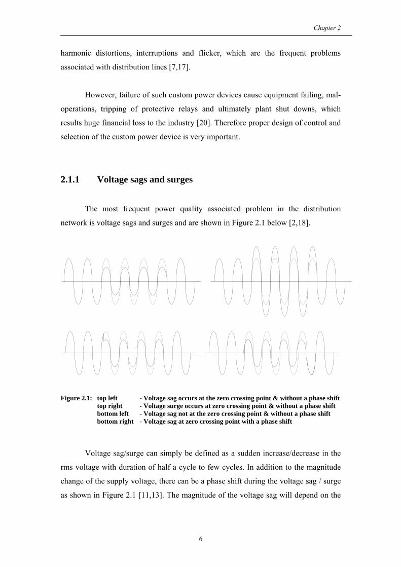
2.1.1 Voltage sags and surges
The most frequent power quality associated problem in the distribution
network is voltage sags and surges and are shown in Figure 2.1 below [2,18].
Figure 2.1: top left - Voltage sag occurs at the zero crossing point & without a phase shift top right - Voltage surge occurs at zero crossing point & without a phase shift bottom left - Voltage sag not at the zero crossing point & without a phase shift bottom right - Voltage sag at zero crossing point with a phase shift
Voltage sag/surge can simply be defined as a sudden increase/decrease in the
rms voltage with duration of half a cycle to few cycles. In addition to the magnitude
change of the supply voltage, there can be a phase shift during the voltage sag / surge
as shown in Figure 2.1 [11,13]. The magnitude of the voltage sag will depend on the
6

Chapter 2
fault type and the location and also on the fault impedance [19]. The duration of the
fault depends on the performance of the relevant protective device [3].
Further it has been found that the voltage sags with magnitude 70% of the
nominal value are more common than the complete outages [35]. Sags and surges can
be identified by the voltage magnitude and the time duration it prevails. IEEE 519-
1992, IEEE 1159-1995 describes it as in Table 2.1 [10].
Disturbance Voltage Duration
Voltage Sag 0.1 – 0.9 pu 0.5 – 30 cycle
Voltage Swell 1.1 – 1.8 pu 0.5 – 30 cycle Table 2.1 : IEEE definitions for the voltage sags and swells
For a particular disturbance (voltage sag or swell), if the voltage and time
duration it remains is within the range given in Table 2.1, the custom power devices
are the optimized solution to overcome the problem and compensate for the
abnormality during the time period it prevails [16].
2.1.2 Custom Power Devices
The most common custom power devices to compensate for the voltage sags
and swells are the Uninterruptible Power Supplies (UPS), Dynamic Voltage Restorers
(DVR) and Active Power Filters (APF) with voltage sag compensation facility.
Among those the UPS is the well known. DVRs and APFs are less popular due to the
fact that they are still in the developing stage, even though they are highly efficient
and cost effective than UPSs [3,14,21]. But as a result of the rapid development in the
power electronic industry and low cost power electronic devices will make the DVRs
and APFs much popular among the industries in the near future [1,22].
DVR and APF are normally used to eliminate two different types of
abnormalities that affect the power quality. They are discussed based on two different
load situations namely linear loads and non-linear loads. The load is considered to be
a linear when both the dependent variable and the independent variable shows linear
7

Chapter 2
changes to each other. Resistor is the best example for a linear device. The non-linear
load on the other hand does not show a linear change. Capacitors and inductors are
examples for non-linear devices.
(a) When the supply voltage/current consists of abnormalities, while the load is
linear:
In this case the custom power device together with the defected supply should
be capable of supplying a defect free voltage/current to the load. To be precise the
device should be able to supply the missing voltage/current component of the source.
A reliable device that can be used for the above case (for voltage abnormalities) is the
DVR. It compensates for voltage sags/swells either by injecting or absorbing real and
reactive power [15].
(b) Power supplied is in normal condition with a non linear load:
When non-linear loads are connected to the system, the supply current also
becomes non-linear and this will cause harmonic problems in the supply waveform. In
such situation to make the supply current as sinusoidal, a shunt APF is connected [8].
This APF injects/absorbs a current to make the supply current sinusoidal. Hence the
supply treats both the non-linear load and the APF as a single load, which draws a
fundamental sinusoidal current [23,24].
Figures 2.2a and b show the basic function of the DVR and the shunt APF.
Figure 2.2a & b: Basic operation of DVR (left) and APF (right)
8

Chapter 2
From Figures 2.2a, b and the references [11,15,23,25] it is clear that the DVR
is series connected to the power line, while APF is shunt connected.
Among the custom power devices, UPS and DVR can be considered as the
devices that inject a voltage waveform to the distribution line. When comparing the
UPS and DVR; the UPS is always supplying the full voltage to the load irrespective
of whether the wave form is distorted or not. Consequently the UPS is always
operating at its full power. Whereas the DVR injects only the difference between the
pre-sag and the sagged voltage and that also only during the sagged period. Thus
DVR operating losses and the required power rating are very low compared to the
UPS. Hence DVR is considered as a power efficient device compared to the UPS
[12,22,26].
2.2 Structure of the DVR
The DVR basically consists of a power circuit and a control circuit. Control
circuit is used to derive the parameters (magnitude, frequency, phase shift, etc…) of
the control signal that has to be injected by the DVR. Based on the control signal, the
injected voltage is generated by the switches in the power circuit [11,27]. Further
power circuit describes the basic structure of the DVR and is discussed in this section.
Power circuit mainly comprising of five units as in Figure 2.3 and the function and the
requirement of each unit is discussed below [1,3,11,16,28].
Figure 2.3: DVR Power circuit
9

Chapter 2
2.2.1 Energy Storage Unit
Energy storage device is used to supply the real power requirement for the
compensation during voltage sag. Flywheels, Lead acid batteries, Superconducting
magnetic energy storage (SMES) and Super-Capacitors can be used as energy storage
devices [3,11,13]. For DC drives such as SMES, batteries and capacitors, ac to dc
conversion devices (solid state inverters) are needed to deliver power, whereas for
others, ac to ac conversion is required.
The maximum compensation ability of the DVR for particular voltage sag is
dependent on the amount of the active power supplied by the energy storage devices
[8,13].
Lead acid batteries are popular among the others owing to its high response
during charging and discharging. But the discharge rate is dependent on the chemical
reaction rate of the battery so that the available energy inside the battery is determined
by its discharge rate [11,21].
2.2.2 Voltage Source Inverter
Generally Pulse-Width Modulated Voltage Source Inverter (PWMVSI) is
used. The basic function of the VSI is to convert the DC voltage supplied by the
energy storage device into an AC voltage. In the DVR power circuit step up voltage
injection transformer is used. Thus a VSI with a low voltage rating is sufficient [21].
The common inverter connection methods for three phase DVRs are 3 phase Graetz
bridge inverter, Neutral Point Clamp inverter [21] and H Bridge inverter [11] for
single phase DVRs.
a) Three-phase graetz bridge
This is often called as two-level three-phase inverter. Each leg is switched
according to the PWM technique used. In the case of fundamental switching is used
then the switches are on for a period of 180o with a duty ratio of 50%. The inverter
configuration, switching and output waveforms for the fundamental switching are
10

Chapter 2
shown in Figure 2.4. This is referred to as two-level since the phase output voltage
waveform consists of two output levels; +Vd and 0 Volts [11,29].
Figure 2.4 : Three phase Graetz bridge and its switching arrangements
b) Neutral Point Clamped Inverter
This Neutral Point Clamped (NPC) inverter can be used for higher voltage
levels than the graetz bridge configuration. The phase output voltage waveform
consists of three levels ⎟⎠⎞
⎜⎝⎛ −
2V and 0 ,
2V dcdc Volts. The inverter configuration and the
single phase output waveforms are shown in Figure 2.5.
outp
ut
Figure 2.5: NPC inverter configuration and its switching arrangement
11
Chapter 2
c) H bridge inverter
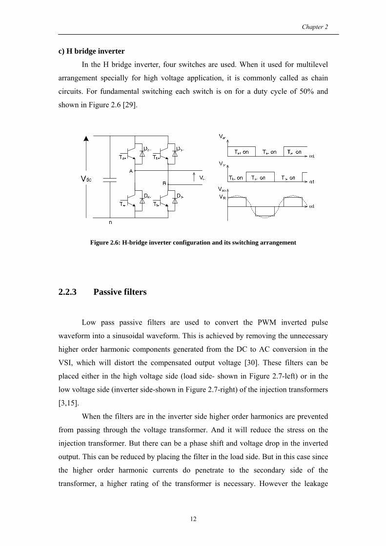
In the H bridge inverter, four switches are used. When it used for multilevel
arrangement specially for high voltage application, it is commonly called as chain
circuits. For fundamental switching each switch is on for a duty cycle of 50% and
shown in Figure 2.6 [29].
Figure 2.6: H-bridge inverter configuration and its switching arrangement
2.2.3 Passive filters
Low pass passive filters are used to convert the PWM inverted pulse
waveform into a sinusoidal waveform. This is achieved by removing the unnecessary
higher order harmonic components generated from the DC to AC conversion in the
VSI, which will distort the compensated output voltage [30]. These filters can be
placed either in the high voltage side (load side- shown in Figure 2.7-left) or in the
low voltage side (inverter side-shown in Figure 2.7-right) of the injection transformers
[3,15].
When the filters are in the inverter side higher order harmonics are prevented
from passing through the voltage transformer. And it will reduce the stress on the
injection transformer. But there can be a phase shift and voltage drop in the inverted
output. This can be reduced by placing the filter in the load side. But in this case since
the higher order harmonic currents do penetrate to the secondary side of the
transformer, a higher rating of the transformer is necessary. However the leakage
12

Chapter 2
reactance of the transformer can be used as a part of the filter, which will be helpful in
tuning the filter [11,15,21].
Figure 2.7: Different filter placements
2.2.4 By-pass switch
Since the DVR is a series connected device, any fault current that occurs due
to a fault in the downstream will flow through the inverter circuit. The power
electronic components in the inverter circuit are normally rated to the load current as
they are expensive to be overrated. Therefore to protect the inverter from high
currents, a by-pass switch (crowbar circuit) is incorporated to by-pass the inverter
circuit [9,11].
Basically the crowbar circuit senses the current flowing in the distribution
circuit and if it is beyond the inverter current rating the circuit bypasses the DVR
circuit components (DC Source, inverter and the filter) thus eliminating high currents
flowing through the inverter side. When the supply current is in normal condition the
crowbar circuit will become inactive [8].
13

Chapter 2
2.2.5 Voltage injection transformers
The high voltage side of the injection transformer is connected in series to the
distribution line, while the low voltage side is connected to the DVR power circuit.
For a three-phase DVR, three single-phase or three-phase voltage injection
transformers can be connected to the distribution line, and for single phase DVR one
single-phase transformer is connected [21]. For the three-phase DVR the three single-
phase transformers can be connected either in delta/open or star/open configuration as
shown in Figure 2.8 [15].
Figure 2.8: Connection methods for the primary side of the injection transformer
Left : delta/open configuration Right : Star/open configuration
The basic function of the injection transformer is to increase the voltage
supplied by the filtered VSI output to the desired level while isolating the DVR circuit
from the distribution network. The transformer winding ratio is pre-determined
according to the voltage required in the secondary side of the transformer (generally
this is kept equal to the supply voltage to allow the DVR to compensate for full
voltage sag) [21]. A higher transformer winding ratio will increase the primary side
current, which will adversely affect the performance of the power electronic devices
connected in the VSI.
The rating of the injection transformer is an important factor when deciding
the DVR performance, since it limits the maximum compensation ability of the DVR
[13]. Further the leakage inductance of the transformer brings to a low value to reduce
14

Chapter 2
the voltage drop across the transformer. In order to reduce the saturation of the
injection transformer under normal operating conditions it is designed to handle a flux
which is higher than the normal maximum flux requirement [21].
The winding configuration of the injection transformer mainly depends on the
upstream distribution transformer.
If the distribution transformer is connected in Δ-Y with the grounded neutral,
during an unbalance fault or an earth fault in the high voltage side, there will not be
any zero sequence currents flow in to the secondary. Thus the DVR needs to
compensate only the positive and negative sequence components. As such, an
injection transformer which allows only positive and negative sequence components
is adequate [4]. Consequently the delta/open configuration can be used (shown in
Figure 2.8-left). Further this winding configuration allows the maximum utilization of
the DC link voltage [11,21].
For any other winding configurations (such as star/star earthed) of the
distribution transformer, during an unbalance fault all three sequence components
(positive, negative and zero) flow to the secondary side. Therefore the star/open
configuration (Figure 2.8-right) should be used for the injection transformers, which
can pass all the sequence components [11,21].
2.3 DVR operating states
2.3.1 During a voltage sag/swell on the line
The DVR injects the difference between the pre-sag and the sag voltage, by
supplying the real power requirement from the energy storage device together with
the reactive power. The maximum injection capability of the DVR is limited by the
ratings of the DC energy storage and the voltage injection transformer ratio. In the
15

Chapter 2
case of three single-phase DVRs the magnitude of the injected voltage can be
controlled individually. The injected voltages are made synchronized (i.e. same
frequency and the phase angle) with the network voltages [16].
2.3.2 During the normal operation
Since the network is working under normal condition the DVR is not injecting
any voltages to the system. In that case, if the energy storage device is fully charged
then the DVR operates in the standby mode or otherwise it operates in the self-
charging mode. The energy storage device can be charged either from the power
supply itself or from a different source [11,21].
2.3.3 During a short circuit or fault in the downstream of the
distribution line
In this particular case as mentioned in section 2.2.4 the by-pass switch is
activated to provide an alternate path for the fault currents. Hence the inverter is
protected from the flow of high fault current through it, which can damage the
sensitive power electronic components [8,16].
2.4 DVR compensation techniques
The compensation control technique of the DVR is the mechanism used to
track the supply voltage and synchronized that with the pre-sag supply voltage during
a voltage sag/swell in the upstream of distribution line. Generally voltage sags are
associated with a phase angle jump in addition to the magnitude change [21].
Therefore the control technique adopted should be capable of compensating for
16

Chapter 2
voltage magnitude, phase shift and thus the wave shape. But depending on the
sensitivity of the load connected downstream, the level of compensation of the above
parameters can be altered. Basically the type of load connected influences the
compensation strategy. For example, for a linear load, only magnitude compensation
is required as linear loads are not sensitive to phase angle changes [11,13].
Further when deciding a suitable control technique for a particular load it
should be considered the limitations of the voltage injection capability (i.e. the rating
of the inverter and the transformer) and the size of the energy storage device [11].
Compensation is achieved via real power and reactive power injection.
Depending on the level of compensation required by the load, three types of
compensation methods are defined and discussed below namely pre-sag
compensation, in-phase compensation and energy optimization technique.
The circuit for a simple power system with a DVR is shown in Figure 2.9
below. The supply voltage, Load voltage, Load current and the voltage injected by the
DVR are denoted by Vs , Vload , Iload and VDVR respectively.
Figure 2.9: Simple power system with a DVR
When the system is in normal condition, the supply voltage (Vs) is identified
as pre-sag voltage and denoted by Vpre-sag. In such situation since the DVR is not
injecting any voltage to the system, load voltage (Vload) and the supply voltage will be
the same.
During voltage sag, the magnitude and the phase angle of the supply voltage
can be changed and it is denoted by Vsag. The DVR is in operative in this case and
the voltage injected will be VDVR. If the voltage sag is fully compensated by the DVR,
the load voltage during the voltage sag will be Vpre-sag.
17

Chapter 2
2.4.1 Pre-sag compensation
This compensation strategy is recommended for the non-linear loads (e.g.:
thyristor controlled drives) which needs both the voltage magnitude as well as the
phase angle to be compensated. In this technique the DVR supplies the difference
between the pre-sag and the sag voltage, thus restore the voltage magnitude and the
phase angle to that of the pre-sag value. Figure 2.9 below describes the pre-sag
compensation technique [11,13]. However this technique needs a higher rated energy
storage device and voltage injection transformers.
Figure 2.10: Pre-sag compensation technique
2.4.2 In-phase compensation
The DVR compensates only for the voltage magnitude in this particular
compensation method, i.e. the compensated voltage is in-phase with the sagged
voltage and only compensating for the voltage magnitude. Therefore this technique
minimizes the voltage injected by the DVR. Hence it is recommended for the linear
loads, which need not to be compensated for the phase angle [11,13]. This particular
compensation technique is shown in Figure 2.10. It is clear from the Figure 2.10, that
there is a phase shift between the voltages before the sag and after the sag.
18

Chapter 2
Figure 2.11: In-phase compensation technique
It should be noted that the techniques mentioned in 2.4.1 and 2.4.2 need both
the real and reactive power1 for the compensation, and the DVR is supported by an
energy storage device.
2.4.3 Energy optimization technique
In this particular control technique the use of real power is minimized (or
made equal to zero) by injecting the required voltage by the DVR at a 90° phase angle
to the load current. Figure 2.11 depicts the energy optimization technique. However in
this technique the injected voltage will become higher than that of the in-phase
compensation technique. Hence this technique needs a higher rated transformer and
an inverter, compared with the earlier cases [11,13]. Further the compensated voltage
is equal in magnitude to the pre sag voltage, but with a phase shift.
1 The reactive power is generated by converting part of the real power supplied into reactive power (by the reactive components used for the DVR).
19

Chapter 2
Figure 2.12: Energy optimization technique
It is even possible to combine different compensation techniques described
earlier, to achieve better efficiency and ease of controllability. One such technique is
combining both the pre-sag and in-phase compensation method. In the combined
technique the system initially restores the load voltage to the same phase and
magnitude of the nominal pre-sag voltage (pre-sag compensation) and then gradually
changes the injected voltage towards the sag voltage phasor. Ultimately the
compensated voltage is in same magnitude and phase angle with the pre-sag voltage
and slowly its phase angle transferred to to the sagged voltage.
Figure 2.12 gives an idea about the compensation control strategy when both
pre-sag and in-phase compensation techniques are combined. It is clear from the
Figure when the DVR injected voltage is VDVR_1 (at the beginning of the
compensation) the system used pre-sag compensation, and slowly the injected voltage
phasor is moved towards VDVR_4 (in-phase compensation) [11].
20

Chapter 2
Vpre-sag
=V load_1
VsagIload
1pu
load_2
load_3
VDVR_3
VDVR_4
Vload_4
Figure 2.13: Combining both pre-sag and in-phase compensation techniques
2.5 Control techniques used in commercially
available DVRs
Most of the commercially available DVRs use either the in-phase
compensation technique or energy optimization technique, owing to minimal
requirement of real power injection: hence it reduces the capacity of the energy
storage needed. Control technique describes the method used to quantify the DVR
control voltage injected during the compensation. In simple terms it basically detects
the occurrence of voltage sag. Some common control techniques used by DVR
manufacturers are described in this section [11].
Irrespective of the compensation techniques used, there should be a scheme to
track the phase angle and the magnitude of the supply voltage during normal
operation (more specifically positive sequence component of the supply voltage) and
to detect the occurrence of voltage sag. In other words there should be a voltage sag
detection technique (it detects the occurrence of the sag, start and end points, sag
depth and phase shift). Followings are some of the common voltage sag detection
techniques.
21

Chapter 2
Voltage sag detection techniques (i) Fourier transform
(ii) Phase Locked Loop (PLL)
(iii) Vector control (Software Phase Locked Loop –SPLL)
(iv) Peak value detection
(v) Applying the wavelet transform to each phase
Out of the techniques mentioned above only the Fourier transform, Vector
control and wavelet transform methods provide both the voltage magnitude and phase
shift information. PLL method can provide only the phase shift information while
peak value detection technique enables to get the magnitude change (voltage sag)
information. Hence it is possible to combine one or more techniques mentioned above
to obtain accurate voltage sag compensation.
2.5.1 Fourier Transform
By applying Fourier transform to each supply phase, it is possible to obtain the
magnitude and phase of each of the frequency components of the supply waveform in
addition to the fundamental such as magnitude and phase information of the 5th and
7th harmonic components. This is the advantage of this method compared with other
sag detection techniques.
For practical digital implementation ‘windowed fast Fourier transform-WFFT’
is used which has same features as the Fourier transform [4]. Further this method can
easily be implemented in real time control system. The only drawback of this method
is after voltage sag has commenced it can take up to one cycle to return the accurate
information about the sag depth and its phase. The reason is the calculation method
used by WFFT is an averaging technique.
22

Chapter 2
2.5.2 Phase Locked Loop
Generally the DVRs use Phase Locked Loop (PLL) to keep a track of the
frequency and the phase angle of the healthy supply voltage, and thereby any change
from the normal operating condition can easily be detected [11,31]. Phase locked loop
is a closed loop feedback control system, that generates a signal with the same
frequency and the phase angle of the input signal. It consists of an oscillator which
provides the output signal. The PLL internal function can be categorized as phase
detector, variable oscillator and a feedback path. PLL responds to frequency changes
and phase angle changes of the input signal by increasing or decreasing the frequency
of the oscillator until it is matched with those of the reference input signal.
Simplified PLL is shown in Figure 2.13. The phase angle of the input signal is
compared with the feedback output of the oscillator and produces an error signal. The
error signal is generated in the form of voltage signal, proportional to the phase angle
difference between the input and output. The output of the phase detector consists of
harmonic components, thus it has to pass through a low pass filter. But this filtering
can introduce transient delays in detecting the voltage sags, which is undesirable
[4,32].
The controlled voltage output2 of the loop filter is then feed in to the Voltage
controlled oscillator and provides a phase output. This output signal (in the form of a
phase angle) is negatively feedback into the phase detector. The output of the
oscillator is compared with the input and if the two frequencies are different, the
frequency of the oscillator is adjusted to match with the input frequency.
Figure 2.14: Simplified block diagram of a phase locked loop
2 The controlled voltage output of the phase locked loop is a function of frequency.
23

Chapter 2
However reference [3] says that this method to track the phase angle is not
accurate and not suitable for fast synchronization. Further with this method it cannot
return the sag depth information and difficult to implement in real-time [4]. Hence a
more accurate method to detect the phase angle is introduced and referred to as
Software Phase Locked Loop (SPLL).
2.5.3 Software Phase Locked Loop (SPLL) / Vector Control
This is an improved method of PLL principal combining a voltage sag
magnitude detection technique using the principal synchronous frame voltage
quantities. Software implementation of this technique is more accurate, faster
detection of voltage sag and can easily be implemented using Digital Signal
Processing (DSP). This method is also referred to as vector control technique or
simply as the synchronous reference frame model [3,4,11].
It is known that unbalance voltage sags create negative sequence voltages
which will rotate in opposite direction to that of positive sequence voltages. When
considering the concept of synchronous reference frame, the negative sequence
component is assumed to have a frequency of twice the frequency of the fundamental.
When all the sequence components (positive, negative and zero) are present in a
voltage waveform it is difficult to track the positive sequence component and also the
result can be erroneous [3,11]. Hence the major point of the SPLL technique is it can
be used to track only the positive sequence component from the supply waveform and
the block diagram is shown in Figure 2.14 [11,21,22].
Figure 2.15: Block diagram of a Software Phase Locked Loop
24

Chapter 2
The basic principal behind the operation of SPLL is regulating the Vsqn to zero
and to track the phase angle (θ) of the positive sequence voltage of the supply wave
form. Initial phase angle information of the supply waveform is given by this θ. Then
the voltage output of the SPLL will be equal to Vsd. By comparing Vsd with a set
reference point any occurrence of voltage sag magnitude can be detected. The same
way by comparing Vsq with a set reference zero the phase angle jump can be detected.
This is further explained in Figure 2.15. It is clear from the figure, when Vsqn tends to
zero Vsdn is in phase with Vsn (normalized supply voltage), hence any voltage sag can
easily be detected by the system.
α
β
d
q
Vsqn
θ б
γ
Vsαn
ω
ω
Figure 2.16: Simplified phasor representation of SPLL
( ) ( ) ( )
σθγ
γ
γ
γθσθσ
σα
β
==
=→
+=
=−≈−
⎟⎟⎠
⎞⎜⎜⎝
⎛= −
and 0
,0sin ,0
sin
sinsin
tan
22
1
sqn
sqnsdn
sqn
ns
ns
Vwhen
VV
V
VV
Each block in Figure 2.13 can further be described as follows [11]. Step 1
The phase voltages (Vsa, Vsb and Vsc) are converted into stationary reference
frame voltage quantities (Vsα and Vsβ) using the following transformation.
25

Chapter 2
Assumption : )(32 2
sCsBsAsss vvvjvvV ααβα ++=+=
⎥⎥⎥
⎦
⎤
⎢⎢⎢
⎣
⎡
⎥⎦
⎤⎢⎣
⎡−−−
=⎥⎦
⎤⎢⎣
⎡
sc
sb
sa
s
s
VVV
VV
2323021211
32
β
α Eq. 2.1
Step 2
The stationary reference frame voltage quantities are converted into
synchronous rotating reference frame voltage quantities (Vsd and Vsq) rotating by an
angle θ.
⎥⎦
⎤⎢⎣
⎡⎥⎦
⎤⎢⎣
⎡−
=⎥⎦
⎤⎢⎣
⎡
β
α
θθθθ
s
s
sq
sd
VV
VV
cossinsincos
Eq. 2.2
Step 3
The Vsd and Vsq values obtained in step 2 are normalized as follows.
VV
VV
VV
VV
2sq
2sd
sqsqn
2sq
2sd
sdsdn
⎪⎪
⎭
⎪⎪
⎬
⎫
+=
+=
Eq. 2.3
Step 4
The next step is to control the angle θ such that the normalized Vsqn=0. This is
achieved using a PI controller. The response time can be varied by changing Kp and
KI values of the PI controller. Then the output of the PI controller is added to ωs,
angular frequency at rated operating condition. Then pass it through a resettable
integrator to obtain the desired SPLL output θ.
In conclusion SPLL principle can be summarized as follows. The synchronous
reference frame is locked to the positive sequence of the voltage Vs by the principle
of PLL and it produces a voltage vector magnitudes Vd and Vq. The phase angle
(theta) used in the synchronous reference frame calculations is used to generate the
reference voltage vector [15]. When the system is in locked condition with the normal
operating condition Vd becomes same as the voltage vector magnitude and Vq
becomes zero. Therefore any disturbance can be identified as they make deviation on
26

Chapter 2
the Vd and Vq from their normally operated values. This is how the fast detection
normally implemented.
2.5.4 Peak value detection of the supply wave form
The peak value of any waveform is the point at which its gradient tends to
zero. This simple phenomenon is used in this technique. The point at which voltage
gradient is zero is identified as the peak value of the supply voltage [32]. It is
compared with a preset reference voltage. If the voltage difference between the supply
and the reference voltage exceeds a specified value (eg. 10%) then the DVR starts
operating (DVR inject the difference voltage). The voltage gradient can be calculated
as follows.
tvv ttt
δδ−−
=Gradient Voltage Eq. 2.4
tv is the voltage at time instant t and is the voltage at time ttv δ− tt δ− where tδ is a
small time step.
As in reference [32], the drawbacks of this method are the time delay (up to
0.5 sec.) in getting the sag depth information and the noise that would affect the
measurements severely. Further to get the phase shift information a reference
waveform is needed which has to be generated separately.
2.5.5 Applying wavelet transformation
The wavelet transform is similar to the Fourier transform with the basic
difference that in wavelet transform it is possible to represent a signal both in time
domain and frequency domain3, but the integral transform can perform only in one
direction [33]. The shortcomings of this technique are the difficulty in directly
interpreting the results and difficulty in real time implementation [4].
3 Fourier transform is a frequency domain representation of a signal and can perform the integral transform in both directions.
27

Chapter 3
New control technique developed for
single phase voltage sag compensation 3.1 Background
The major drawback of the existing voltage sag detection techniques discussed
in section 2.5 is that, it is costly and complicated to control the voltage injection for a
single phase fault, where most frequent fault occurred in a targeted phase. As such it
will be an easier alternative to control the voltage injection in the phases individually
using three single phase DVRs. In this case the voltage injection in each phase is
controlled independently to the other phases. This arrangement of DVR gives
possibility of installing single-phase DVR if only one phase is identified with frequent
interruptions.
This project mainly focused on designing a control strategy for a single-phase
Dynamic Voltage Restorer to detect single-phase voltage sags. The study has been
carried out only for single-phase voltage sags, since single phase voltage sags are the
most common type of voltage sag occurs in Sri Lanka than the three phase sags. In
case of full compensation required, three of the single-phase DVR arrangement can be
used.
In this project an analogue control system was developed with a combination
of pre-sag and in-phase compensation techniques as discussed in section 2.4. In pre-
sag compensation technique, always load voltage is maintained to be same as the pre-
sag voltage. But this method of compensation requires higher capacity energy storage
28

Chapter 3
device, which will directly affect the cost of the DVR, if the sag continues for a longer
duration. In-phase compensation technique compensates only for the voltage
magnitude and as a result the compensated load voltage will undergo a phase shift if
the voltage sag is associated with a phase jump. Thereby the requirement of a higher
capacity energy storage device can be bargained. In the developed control strategy, at
the beginning of the sag the DVR compensate both for the voltage magnitude change
and the phase shift as well, same as pre-sag compensation and restored the load
voltage back to the pre-sag voltage. Then the controller smoothly transfers the
compensation technique from pre-sag to in-phase technique thus the developed
control plays an intelligent role to minimize the DVR rating while maintaining load
voltage without experiencing any disturbance.
Further to detect the occurrence of voltage sag, peak value of the supply
voltage was constantly monitored. The measurement method was discussed under
section 2.5.4.
It is important to note that the small frequency variations (within the allowable
range defined by IEEE) of the supply voltage is tolerable and can be tracked by this
control mechanism without any compensation. The frequency variations beyond the
defined range (±1%) are assumed to be taken care by the system control of the utility.
3.2 Simplified control block diagram
Voltage sag is produced by a magnitude change with or without a phase shift
of the supply voltage. Thus it is necessary to quantify and correct for phase shift (if
any) prior to compensate for the voltage sags. To quantify the phase shift a random
reference phase angle waveform was generated and by using a feedback control loop
the error (between the supply and the reference phase angle waveforms) was regulated
to zero. Therefore at the steady operation of the control the reference waveform was
tracked to the supply and both are synchronized in phase angle.
29

Chapter 3
Then the reference voltage waveform was created from the reference phase
angle and rated rms load voltage. Finally, the voltage that needed to be injected by the
DVR was calculated by subtracting the measured supply voltage from the reference
voltage waveform.
The control block diagram related to the above is shown in Figure 3.1 below.
Block 1 Block 2 Block 3 Block 4
Find the phase angle of the reference voltage
Calculation of control voltage
Generation of the reference
voltage waveform
Find the phase angle of the
supply waveform
Figure 3.1: Simplified control block diagram for the single phase DVR
Each block was implemented using EMTDC/PSCAD software for the
simulation and construction method of each block is described below.
3.3 PSCAD implementation of control circuit
3.3.1 Block 1: Determination of supply voltage phase angle
Since the supply voltage waveform is measured and readily available, it is
possible to obtain all the information (magnitude, frequency) related to the supply.
Consequently the starting and ending point of each cycle can be easily obtained.
During each cycle the phase angle of the input voltage waveform is varying from 0
rad to 2π rad (0˚ to 360˚). Thus the phase angle waveform of the supply voltage
(Ameas) can be obtained. Figure 3.2 shows the implementation method of the block 1.
Figure 3.3 shows the schematic diagram of the block 1 using EMTDC/PSCAD
package.
30

Chapter 3
Phase angle of the supply voltage
Rated frequency
Clear signal to the integrator
Resettable integrator 2πf
Supply voltage waveform
Zero crossing point detection
Limiter
Figure 3.2: Implementation method of block 1
ZeroDetector
Vs
Clear
1sT314.1593 Ameas
Clear_signal
Inpu
t
ZCD
Figure 3.3: PSCAD implementation of block 1
As shown in Figure 3.3, the input signal to this integrator is the angular
frequency of the input waveform, i.e. the 2πf=314.1593 (constant), with f being the
nominal supply frequency 50Hz. Then the output supply phase angle waveform (or
the integrator output) is a line with a gradient of 314.1593(or y=314.1593.t shape)1.
This signal is re-setted at every supply cycle in order to obtain the phase angle
information. This re-set function is achieved by introducing a clear signal. The clear
signal is obtained from the positive zero crossing detector, made of zero crossing
detector with positive side limiter, of the supply waveform This will ensure the clear
signal is activated per cycle.
Different components parameters of the above Figure 3.3 were selected as follows.
1 When a constant of magnitude m is integrated with respect to time the output will be in the form of y=mt, where m being the gradient of the linear output signal.
31

Chapter 3
1) Supply voltage (Vs): This is the input voltage signal from the particular supply
phase feed from the distribution transformer. 240 V, 50 Hz sinusoidal input source
with an internal series impedence of 0.01 Ω was taken. During the sag this input
voltage reduced depending on the severity of the upstream fault.
2) Zero crossing detector (ZCD): This component produce an output of 1, when the
input crosses the zero value axis at its positive gradient and -1 at the negative
gradient zero crossing point. At all the other times the output will be zero. This is
shown in Figure 3.4.
Figure 3.4: Integrator clear signal generation
3) Limiter: This limits the negative signal. Thus this will detect only the positive
part of the zero crossing detector’s output signal. This enables to detect the cycle
time of the supply voltage waveform. The output (as in Figure 3.5) is directly feed
into the integrator as the clear signal.
32

Chapter 3
Figure 3.5: Integrator clear signal
4) Resettable integrator: This unit simply performs the integration function
together with resetting to a predetermined value when the clear signal is present.
The input signal is 2πf (f = 50 Hz). The integrator time constant was selected as
1s. This outputs the phase angle information of the supply voltage waveform and
the output waveform is shown in Figure 3.6.
Figure 3.6: Phase angle variation of the supply voltage
PSCAD output waveforms at different output channels are shown in figure 3.7
and 3.8 below.
33

Chapter 3
Implementation of Block 1
time(s) 0.450 0.460 0.470 0.480 0.490 0.500 0.510 0.520 0.530
-1.00
-0.75
-0.50
-0.25
0.00
0.25
0.50
0.75
1.00
vol
tage
(kV)
& p
hase
ang
le (r
ad)
Supply voltage ZCD Clear_signal Angle meas*0.1
Figure 3.7: Output waveforms at different output channels
Phase angle of the supply waveform (Angle measured) is de-rated by a factor
of 0.1 to show all the waveforms in a single plot. When the supply is in the normal
condition the actual maximum height of the Angle measured waveform is 6.283 (2πft,
where t = 0.02 s, cycle time related to 50 Hz). Implementation of Block 1
time(s) 0.450 0.460 0.470 0.480 0.490 0.500 0.510 0.520 0.530
314.050 314.075 314.100 314.125 314.150 314.175 314.200 314.225 314.250 314.275
Input signal to the resettable integrator
Figure 3.8: Input waveform to the resettable integrator
34

Chapter 3
3.3.2 Block 2: Reference phase angle waveform generation
I
P
D +
F
-
D +
F
-Aref
314.1593 Aref
A
B
Compar-ator
6.2832Ameas
Clear
1sT
Ang
le E
rror
Ameas
A
BCtrl
Ctrl = 1
0.0
triggering pulse
Angl
e Er
ror i
nput
Angle Error filtered
PI output
*10.0
Figure 3.9: Simulation block for the reference phase angle wave form generation
In the block as shown in Figure 3.9, a random reference phase angle signal is
generated. The reference signal’s phase angle is synchronized with the measured
signal phase angle by slowly adjusting the gradient (angular frequency) of the
randomly generated reference phase angle signal.
The simulation block diagram shown in Figure 3.9 consists of 3 major blocks
and is shown in Figure 3.10 and discussed in 3.3.2.1-3.
AmeasCalculate the angle error
and regulate it to zero
Generate the
new Aref
Adjust the gradient of Aref
according to angle error
Figure 3.10: Simplified diagram of control block 2
3.3.2.1 Calculate the angle error between the reference and the supply phase
angle.
Initially a random reference phase angle wave from was created for a
frequency of 50Hz. Then a simple comparator block was used to calculate the angle
error. As seen in the Figure 3.11 below the angle error between the two waveforms
35

Chapter 3
are varying from positive to negative during each cycle. Further the average error is
zero.
Reference phase angle Measured phase angle
Angle error
Average angle error = 0 Figure 3.11: Generation of angle error signal
Filtered and PI controlled output of this angle error has to be added or
subtracted from the reference (314.1593). As shown in Figure 3.10, the next step is to
adjust the gradient of the Aref to synchronize it with the Ameas, while regulating this
angle error component to zero. Inability to identify whether this error component has
to be added or subtracted (since it varying from positive to negative during each
cycle) introduces an additional control block and separately shown in Figure 3.12.
to the filter etc..
Ameas
A
BCtrl
Ctrl = 1
0.0
triggering pulse
Ang
le E
rror
inpu
t
*10.0
Angle error
Figure 3.12: additional block to obtain the angle error
36

Chapter 3
The measured phase angle waveform was fixed during the normal operation.
Hence it can be used as a reference to calculate the angle error. Two points closer to
the middle of the phase angle waveform (2.5 rad to 3.5 rad) were selected and when
the measured phase angle waveform is within those limits, the block calculates the
angle error. When the measured phase angle was beyond the given limit the block
doesn’t calculate any angle error. This technique is used mainly to get the error which
clearly differentiates the angle lead or lag and proportional to its magnitude. A range
comparator was used to achieve this task and its specifications are as shown in Figure
3.12.
Comparator will generate an output of 1 when the input (supply phase angle in
radians) is between 2.5-3.5. Except this limits, it will generate a zero output as angle
error. When selecting the comparator limits care has to be taken to maintain the same
magnitude of the angle error. (i.e. within the selected limit the angle error should not
change its sign.)
Figure 3.13: Angle error calculation
It is clear from Figure 3.13; the angle error is definitely a negative value (or
can be definitely positive either if Aref is leading Ameas) as the points considered are
37

Chapter 3
only between 2.5 rad to 3.5 rad. If the comparator limits were selected closer to the
ends such as 0 rad or 6.2832 rad then the angle error varies its sign, which is not
desirable.
A two way input selector switch was used to generate an output only when the
triggering pulse is present i.e. when it is 1. The obtained angle error was multiplied by
a factor 10 to speed up the synchronization and obtain more accurate synchronization.
Then the angle error signal was passed through a filter and a PI controller.
3.3.2.2 Regulate the error component and reduce the harmonics
The angle error wave form obtained above is a pulsed waveform consists of
harmonics. To achieve better synchronization the error has to be regulated to zero,
while converting the pulse signal into a smooth one. A low pass LC filter and a PI
control was added to achieve that purpose and explained below.
3.3.2.3.1 Low pass filter
A filter with a second order transfer function was used. It attenuates the
frequencies above the characteristic frequency. A 500 Hz was selected as a reasonable
value for the characteristic frequency. This passes the frequency components below
the 500 Hz which will attenuate the harmonics to a reasonable level. Gain and the
damping ratio of this low pass filter were selected to be 1 to maintain the same
magnitude and the wave shape of the input during filtering.
3.3.2.3.2 PI controller
A Proportional Integrate controller was used to regulate the error between the
measured (supply) and the reference phase angle to zero.
Reasons for selecting a PI controller
38

Chapter 3
The function of the proportional action is to respond quickly to the changes in
the error deviation. Integral action is slower than the proportional response but used to
remove the offsets between the input and the reference at steady state [34]. Before the
DVR starts injecting voltage to the system, a considerable time period was allowed
for the synchronization. The synchronization process was made according to the
possible system frequency deviation. As the system frequency is not much deviate
from 50 Hz the fast synchronization is not a necessity. Hence it helps the load voltage
without phase jump. Therefore the derivative action is not needed and the need of PID
controller was omitted2.
Tuning the PI controller
In the PSCAD simulation block for the PI controller following parameters has
to be defined as shown in Figure 3.14.
Figure 3.14: User defined parameters in the PI controller
Among those parameters proportional gain (Kp) and the integral time constant
(KI) directly affect the performance of the PI controller. When tuning those two
parameters special attention has to be paid. The maximum and the minimum limits of
the PI controller was selected, as the output at any instant doesn’t exceed those two
values. (+10 and -10) At the beginning of the simulation (at t=0) the controller set to
zero output. Hence the initial output is assigned to zero.
2 The derivative action of the PID controller speeds up the system response.
39

Chapter 3
Tuning the Kp and KI parameters of the PI controller
Initially KI (Integral time constant) was set at a high value and the simulations
were carried out for different Kp values. It has been observed that with increasing Kp
the time taken to reach the target decrease, Kp=0.5 was selected as reasonable. Then
by reducing the KI the simulation results were observed. The PI output reaches the
target and stabilizes after longer time. Hence KI was selected as 0.2, which is same as
5sec time constant.
3.3.2.3 Generating the reference phase angle
As described earlier when considering the waveforms of Aref and Ameas
there are two possibilities. In the first case measured phase angle leads the reference
phase angle. In this case the angle error input is negative; hence the PI controller
output will also become negative. To get the waveforms synchronized the gradient of
the Aref has to be increased: the PI controller output (negative) has to be subtracted
from the set gradient point (314.1593). This will happen automatically in the control
as the adder is used and PI controller out put is negative. In the second case measured
phase angle lags reference phase angle. In this case the angle error input is positive;
hence the PI controller output will also become positive. To get the waveforms
synchronized the gradient of the Aref has to be reduced: the PI controller output
(positive) has to be subtracted from the set gradient point (314.1593). For example
synchronization in both cases are described in the following Figure 3.15.
40

Chapter 3
Figure 3.15: Synchronization process
The next step is to generate the reference phase angle waveform. The gradient
of the reference signal is known and the reference phase angle should vary from 0 to
2π (6.2832) radians. Therefore the reference phase angle waveform should be cleared
when it reaches 2π. A comparator and a resettable integrator are used to achieve this
resetting. The integrator clear signal is given by the comparator output. This block is
shown in Figure 3.16 together with the comparator specifications.
Aref
A
B
Compar-ator
6.2832
Clear
1sToutput of the summing/
differncing junction
Figure 3.16: Left: Reference waveform generation Right: Comparator specifications
The function of the above block is similar to block 1 described in 3.3.1. The
comparator compares the magnitude of the Aref signal with the set value (6.2832) and
41

Chapter 3
when the Aref > 6.2832, the integrator clear signal is reset and thus the integrator
output set to zero.
3.3.3 Block 3: Reference voltage waveform generation
The reference phase angle was generated and synchronized with the supply
(measured) phase angle. Next step is to generate the reference voltage waveform from
the reference phase angle information. From the phase angle information obtained a
sinusoidal waveform was generated with the nominal supply voltage magnitude as in
Figure 3.17. (240V rms = 340V peak)
Figure 3.17: Reference voltage waveform generation
The simulation control block is shown in Figure 3.18.
Aref VrefSin *
0.34
Figure 3.18: Simulation block for reference voltage waveform generation
42

Chapter 3
3.3.4 Block 4: Control voltage waveform generation
The block no. 4 was used to calculate the control voltage by taking the
difference between the reference and the supply voltage. When the supply voltage is
in normal condition (no voltage sag), both the supply and the reference voltage
waveforms are in phase and same in magnitude thus the voltage to be injected by the
DVR circuit would be zero.
The control voltage will be present only during the voltage sag. The shape of
the control voltage waveforms for different sag conditions are shown in Figures 3.19.
0 0.005 0.01 0.015 0.02 0.025 0.03 0.035 0.04-0.25
-0.2
-0.15
-0.1
-0.05
0
0.05
0.1
0.15
0.2
0.25
time (sec)
Vol
tage
(kV
)
Control voltage during the voltage sag (reference and the supply voltages are not in phase)
reference voltage
supply (sag) voltage
control voltage
0 0.005 0.01 0.015 0.02 0.025 0.03 0.035 0.04-0.25
-0.2
-0.15
-0.1
-0.05
0
0.05
0.1
0.15
0.2
0.25
Control voltage during the voltage sag (both the reference and the supply are in phase)
time (sec)
Vol
tage
(kV
)
referencevoltage
Control voltage
supply(sag) voltage
0.25
0 0.005 0.01 0.015 0.02 0.025 0.03 0.035 0.04-0.25
-0.2
-0.15
-0.1
-0.05
0
0.05
0.1
0.15
0.2
Control voltage before the voltage sag (both the reference and the supply are in phase)
time (sec)
Vol
tage
(kV
)
reference and thesupply voltagesare the same Figure 3.19 top: Control voltage
waveform before the voltage sag Figure 3.19 bottom left: Control voltage waveform during the sag (in phase voltage sag) Figure 3.19 bottom right: Control voltage waveform during the sag (voltage sag is created with a phase shift)
zero control voltage
43

Chapter 3
It is clear from the above figures irrespective of the type of voltage sag (in phase or
not with the reference voltage) the control voltage is a pure sinusoidal waveform with
varying magnitude during the sag period.
The simulation block diagram is shown in figure 3.20.
D +
F
-
Vs
Vref
Vcontrol
A
BCtrl
Ctrl = 1
0.0
TIME
Figure 3.20: Simulation draft for block 4
When implementing this block in PSCAD simulation software a time delay of
4 sec. was introduced due to following reasons. (i.e. when the DVR is switched on,
during the first 4 sec. the DVR control is disengaged internally while synchronization
process is activated)
1. to eliminate unnecessary starting transients in the simulation or in practice
2. to allow the supply voltage and the reference voltage to get synchronized.
The block shown in dashed lines is used to provide the time delay switching
signal to start operation of the DVR. When the input time signal is above the specified
value the comparator will generate a signal of 1 and 0 otherwise. When the
comparator output is 1 the block starts calculating the control voltage that needs to be
injected by the DVR circuit.
Further it should be noted that in the simulation, the synchronization time
depends on the initial phase shift between the supply voltage and the internally
generated reference voltage and also the parameters of the PI controller. If both the
44

Chapter 3
wave forms are in phase at the beginning, then theoretically two waveforms should
get synchronized from the beginning itself since the angle error is zero. But it was
realized that due to the involvement of the feedback control loop and its initial setting
values, still it takes some time for synchronization. By considering all of theses
effects, to eliminate the start up transients it has given 4 seconds in the simulation to
synchronize and stabilize the controller action. There after the controller will be ready
for the DVR operation.
In the block 4, the voltage that needs to be injected to the DVR was calculated.
Next step is to create a power circuit consisting of the units described in section 2.2,
which is capable of generating the above calculated control voltage.
3.4 PSCAD implementation of the power circuit
The power circuit of the single phase DVR mainly consists of Energy storage
device, inverter, filter and a voltage injection transformer and is shown in Figure 3.21.
Figure 3.21: Power circuit of the DVR
45

Chapter 3
Suitable values for VDC, C1, LF, CF, Rs, Rl and transformer turn ratio n have to be
determined.
3.4.1 Parameter estimation of the power circuit
Capacitor C1 is used as a DC link capacitor, and C1=10,000 μF is assumed to
be a reasonable value as it is used with the batteries. The power circuit shown in
Figure 3.21 was simplified as in Figure 3.22 and for the parameter estimation
purposes Figure 3.23 was used.
Figure 3.22: Simplified equivalent circuit of DVR power circuit
Figure 3.23: Equivalent circuit used for parameter estimation
46

Chapter 3
If the DVR is capable of compensating for a full voltage sag (when Vsup=0)
then,
Vinj_max =Vs=240V rms.
For voltage transformer, 1
1 1II
nVV L
inj
==
Assumed that the fundamental component of the current is flowing through
the XCF is small.
LFinj
LFinj XjIn
VXjIVE 111 +=+= Eq. 3.1
For safety point of view n is kept at a high value to maintain a low voltage at
the primary side of the transformer. Therefore the turn ratio of the transformer is
selected as 4.
Then,
VVEVE
EV
VV
DCinj
inj
injpeak
peak
100 but, value.reasonable a is 100
(1) from
31.814
2230
_1
_1
==
≈∴
<
==
3.4.1.1 Energy storage device
Two batteries of 50V each are used to provide the real power requirement
during the voltage sag compensation.
3.4.1.2 PWM inverter
Two-leg inverter consisting four IGBTs and four diodes are used for single
phase voltage sag detection. Inverter legs are switched on and off accordingly, such
that the desired control voltage can be obtained at the filter output point.
47

Chapter 3
3.4.1.2.1 Inverter leg switching signal generation
The control voltage output, obtained and described in section 3.3.4, is
compared with a high frequency triangular waveform with a switching frequency of
5000Hz and a 100V peak output with a 50% duty cycle. High value of switching
frequency (5000Hz) was selected to suppress the DVR injected voltage harmonics
transferring to the load voltage in addition to voltage sag compensation.
As can be seen from the Figure 3.24, the control voltage was reduced by a
factor of 4, before comparing it with the triangular waveform to compensate for the
transformation ratio of the voltage injection transformer. The level comparator
produces two output levels as shown in Figure 3.25.
Tri
PtopA
B
Compar-atorTri Pbot
Vcontrol*
0.25 Vcontrol1 Figure 3.24: Inverter leg switching signal generation
1) Comparator generates an output of 1, when the magnitude of the triangular
waveform is higher than that of the control voltage. (Tri > Vcontrol 1)
2) Produces a zero output when triangular waveform is lower than or equal to control
voltage at the selected point. (Vcontrol 1 ≤ Tri)
48

Chapter 3
Figure 3.25: Switching signals for inverter legs
The output signal of the comparator (Pbot) and the NOT operated inversion
(Ptop) is fed into the inverter legs.
To achieve a smooth control voltage (= injected voltage to the power line) and
to filter out the unwanted higher order harmonic components from that waveform a
LC filter was connected at the output of inverter.
3.4.1.3 Designing and tuning of the low pass filter
Cut-off frequency (f) of a simple LC filter is given by the following equation.
LC21f
π= Eq. 3.2
Cut-off frequency should lie between the supply frequency (50Hz) and the
modulating triangular waveform frequency (5000Hz). Therefore 500Hz was selected
49

Chapter 3
as the cut-off frequency and capacitor value was calculated assuming L = 0.6 mH. By
applying L and f values to equation 3.1, the capacitor value was obtained as 168μF.
But during the simulation it has been identified that with the above calculated
LC values the compensated voltage could not block the harmonic up to the required
level. It has been observed that by modifying the filter, the quality of the output
waveform could be improved to a certain level. Therefore the filter configuration
shown in Figure 3.21 was slightly modified as in Figure 3.26 to remove the harmonic
effect.
Figure 3.26: Low pass filter configuration
For simplicity it has been assumed that the inductor value is halved for the
new filter configuration, while keeping the same value for capacitance. The DVR side
inductor smoothes the waveform while the grid side inductor block the harmonic
injection.
Further it has been observed that, better performance of the DVR could be
obtained by increasing the capacitance. After comparing the results of several
simulations for different Capacitances 1000μF was selected as a reasonable value.
Therefore subsequent simulations the capacitance value is taken as 1000μF.
3.4.1.4 Voltage injection transformer
Ratio of the voltage transformer was selected as 60V:240V (discussed in
section 3.4.1) such that the DVR is capable of compensating the full voltage sag,
provided the DC storage device is capable of supplying the full real power
requirement during the compensation. Hence 100 kVA rated transformer with 1:4
turns ratio was selected.
50

Chapter 3
Specifications of the voltage injection transformer selected are shown in
Figure 3.27.
Figure 3.27: Configuration data of the voltage injection transformer 3.4.2 Voltage sag generation
The voltage sag was created in the distribution line by switching on a shunt
connected circuit breaker together with a series reactance. This can either be a
resistance, inductance or a combination. In this case for simplicity of calculations
resistive fault impedance was taken for the fault and grid. This is presented in Figure
3.28.
51

Chapter 3
0.01
100.0
Vs
Iload
VL
BR
K
VInj
0.01
#1 #2From the low pass filter
BRK
TimedBreaker
LogicOpen@t0
Shunt connected circuit for voltage sag generation
Figure 3.28: Left: Generating voltage sag for the power circuit, Right: Breaker parameters
From Figure 3.28 left, it is clear that the circuit breaker is initially in open
position. As such there will be no sag voltage applied. To create the sag the breaker
was closed at t = 5.21sec and the sag is remained for 70 msec. For further analysis the
above circuit simplified as shown in Figure 3.29
Vs - Source voltage (240V rms)
Rs - Source resistance (0.01 Ω)
Vsag - Magnitude of the voltage sag (V)
Vinjected - Voltage injected by the DVR (V)
VL - Load Voltage (V)
Figure 3.29: Equivalent circuit for the distribution line
Before the voltage sag, the circuit breaker is kept at open position. An open
circuited path was created across the breaker. As the system is under normal
condition, the DVR is not injecting any voltage to the distribution line (Vinjected=0V).
The equivalent circuit for the above is as follows in Figure 3.30.
52

Chapter 3
Ls
LsL
LbeforeL
Ls
sbefore
RRRVV
RIV
RRVI
n
n
+=
⋅=
+=
Figure 3.30: Equivalent circuit before the voltage sag
Assume a case when the voltage sag is present, but the DVR is not connected
to the circuit as in Figure 3.31.
sagLsagLs
LsagsL2sagL
sagL
sagsag2
sagL
sagLs
s
sagLs
ssag
RR)RR(RRRV
RIV
RRR
II
RRRR
R
V)R//R(R
VI
⋅++
⋅⋅=⋅=
+⋅=
⎟⎟⎠
⎞⎜⎜⎝
⎛
+
⋅+
=+
=
Figure 3.31: Equivalent circuit during the voltage sag
This analysis shows that by changing Rsag parameter, the magnitude of the sag
can be altered. The typical values selected for the simulation was RL=100Ω and
Rsag=0.01Ω. It can be seen that RL>>>>Rsag.
Hence, 11RR
sag
L >>>>+
sagLV can further be simplified as follows.
nLsagL
nLLs
Ls
Ls
Ls
L
1
sag
Ls
Ls
Lsag
sagLs
LssagL
VV ,
VRR
RV
RRRV
R1RRR
RV
RR
)RR(RRV
V
hence
but,
<
=+⋅
+⋅
<
+⎟⎟⎠
⎞⎜⎜⎝
⎛+⋅
⋅=
++⋅
=
>>>>43421
53

Chapter 3
The load voltage during the sag is less than the healthy load voltage.
Then ; which is the voltage injected by the DVR during the sag
period.
sagLnLinj VVV −=
3.4.2.1 Different sag and loading conditions
The above calculations were performed assuming both the Rsag and RL are
resistive loads. By changing the magnitude and the type of the shunt connected fault
impedance, the severity of the voltage sag can be changed. For example, if an
inductive impedance is connected having the same reactance, (2πfL=Rsag ), the
voltage sag can be created with the same magnitude but with a phase shift. The
simulations were carried out by considering the following sag and loading conditions.
(i) Sag without a phase shift and the sag was created at the zero crossing point of the
voltage waveform.
(ii) Sag without a phase shift and the sag was created not at the zero crossing point of
the voltage waveform.
(iii) Sag with a phase shift and the sag was created at the zero crossing point of the
voltage waveform.
(iv) Sag with a phase shift and the sag was created not at the zero crossing point of
the voltage waveform.
The loading conditions were changed by connecting,
(i) Pure resistive load of magnitude 100Ω.
(ii) Pure inductive load with the same reactance. (2πfL=RL)
(iii) Combination of resistive and inductive load with a 0.8 power factor.
3.4.3 Harmonic effect
During the PSCAD simulation the supply voltage maintained as a pure
sinusoidal waveform. But in the practical environment this condition is no longer
valid. The supply voltage contains harmonic components. To identify the harmonic
54

Chapter 3
components present in the supply, a harmonic analysis was carried out for practical
the supply voltage using a digital power meter available in the laboratory. The
measured harmonic components and their magnitudes are shown in below Table 3.1.
Harmonic component
Magnitude (V rms)
Harmonic component
Magnitude (V rms)
Fundamental 234.86* 26 0.02 2 0.2* 27 0.12 3 2.98* 28 0.02 4 0.17 29 0.11 5 4.2* 30 0.02 6 0.05 31 0.08 7 4.12* 32 0.01 8 0.09 33 0.09 9 1.36* 34 0.01 10 0.07 35 0.07 11 1.78* 36 0 12 0.03 37 0.05 13 0.58* 38 0.01 14 0.06 39 0.03 15 1.04* 40 0 16 0.03 41 0.06 17 0.41* 42 0 18 0.02 43 0.04 19 0.81* 44 0 20 0.01 45 0.03 21 0.18* 46 0 22 0.03 47 0.04 23 0.34* 48 0 24 0.02 49 0.01 25 0.14* 50 0
Table 3.1 : Harmonic content in the normal supply voltage
The shape of the supply waveform with healthy and with those harmonics was
simulated in PSCAD and is shown in Figures 3.32 and 3.33 together with the
simulation block.
55

Chapter 3
Time ... 0.0000 0.0050 0.0100 0.0150 0.0200 0.0250 0.0300 0.0350 0.0400
-0.40 -0.30
-0.20 -0.10
0.00 0.10 0.20
0.30 0.40
Volta
ge (k
V)
Supply voltage (healthy)
-0.40 -0.30
-0.20 -0.10 0.00 0.10
0.20 0.30 0.40
Volta
ge (k
V)
Supply voltage (with harmonics)
Figure 3.32: Top: Supply voltage waveform without harmonics
Bottom: Supply waveform with harmonics
Supply voltage (with harmonics)Vs
0.01 0.01 0.01 0.01
100.0
Vs
0.01 0.01
Fundamental 2nd 3rd 4th 23rd 25th
Load
Figure 3.33: PSCAD implementation of supply harmonics Due to the limitations in implementing all the harmonic components in PSCAD only
marked “*” major 15 harmonics were considered for the simulation. Those harmonic
components were added to the supply voltage as shown in Figure 3.43 and observed
the effect on the load voltage by introducing voltage sag.
56

57
Chapter 4
Results and Discussion
The simulation is carried out and the results are analyzed for different voltage
sag and load conditions as discussed in chapter 3 and briefly given below.
Different voltage sag conditions
(i) Sag without a phase shift and the sag created at the zero crossing point of the
voltage waveform.
(ii) Sag without a phase shift and the sag created not at the zero crossing point of the
voltage waveform.
(iii) Sag with a phase shift and the sag created at the zero crossing point of the voltage
waveform.
(iv) Sag with a phase shift and the sag created not at the zero crossing point of the
voltage waveform.
The loading conditions were changed as follows.
(i) Pure resistive load of magnitude 100Ω.
(ii) Pure inductive load with the same reactance. (2πfL=RL)
(iii) Combination of resistive and inductive load with a 0.8 power factor.
To simplify the analysis the simulations were carried out under the following
different cases as shown in Table 4.1.

Chapter 4
58
Sag criteria Load criteria Harmonics Sy
stem
Subs
yste
m
Faul
t [1
]
Phas
e sh
ift
[2]
Star
t at[3
]
Tim
e
dura
tion
(s)
[4]
Load
ty
pe[5
]
PF[6
]
Har
mon
ics
in th
e su
pply
[7]
1a 0.01Ω-R N zc 5.1-5.13 100Ω-R 1 N
1b 0.01Ω-R N nzc 5.105-5.135 100Ω-R 1 N
1c 0.01Ω-R N nzc 5.113-5.143 100Ω-R 1 N 1
1d 0.01Ω-R N nzc 5.102-5.189 100Ω-R 1 N
2a 0.01Ω-R N zc 5.1-5.13 80Ω+0.191H-RL 0.8 N
2b 0.01Ω-R N nzc 5.105-5.135 80Ω+0.191H-RL 0.8 N
2c 0.01Ω-R N nzc 5.113-5.143 80Ω+0.191H-RL 0.8 N 2
2d 0.01Ω-R N nzc 5.102-5.189 80Ω+0.191H-RL 0.8 N
3a 0.03183mH-L Y zc 5.1-5.13 100Ω-R 1 N
3b 0.03183mH-L Y nzc 5.105-5.135 100Ω-R 1 N
3c 0.03183mH-L Y nzc 5.113-5.143 100Ω-R 1 N 3
3d 0.03183mH-L Y nzc 5.102-5.189 100Ω-R 1 N
4a 0.03183mH-L Y zc 5.1-5.13 80Ω+0.191H-RL 0.8 N
4b 0.03183mH-L Y nzc 5.105-5.135 80Ω+0.191H-RL 0.8 N
4c 0.03183mH-L Y nzc 5.113-5.143 80Ω+0.191H-RL 0.8 N 4
4d 0.03183mH-L Y nzc 5.102-5.189 80Ω+0.191H-RL 0.8 N
5a 0.005Ω-R N nzc 5.102-5.189 100Ω-R 1 N
5b 0.005Ω-R N nzc 5.102-5.189 80Ω+0.191H-RL 0.8 N
5c 0.01592mH-L Y nzc 5.102-5.189 100Ω-R 1 N 5
5d 0.01592mH-L Y nzc 5.102-5.189 80Ω+0.191H-RL 0.8 N
6a 0.01Ω-R N nzc 5.105-5.135 50Ω-R 1 N
6b 0.01Ω-R N nzc 5.105-5.135 40Ω+0.096H-RL 0.8 N
6c 0.03183mH-L Y nzc 5.105-5.135 50Ω-R 1 N 6
6d 0.03183mH-L Y nzc 5.105-5.135 40Ω+0.096H-RL 0.8 N
7a 0.01Ω-R N nzc 5.102-5.189 100Ω-R 1 Y
7b 0.01Ω-R N nzc 5.102-5.189 80Ω+0.191H-RL 0.8 Y
7c 0.03183mH-L Y nzc 5.102-5.189 100Ω-R 1 Y 7
7d 0.03183mH-L Y nzc 5.102-5.189 80Ω+0.191H-RL 0.8 Y Table 4.1: Different sag and load criteria

Chapter 4
59
Each system was selected in such a way that covers all possible practical situations
and explained as below:
[1] Describes whether the sag is resistive (R), Inductive (L) or a combination of both
(RL) and the magnitude of it.
[2] This specifies the sag is associated with a phase shift (Y) or not (N). This is a direct
result of criteria [1] above.
[3] Whether the sag has commenced at zero crossing point of the voltage (zc) or not
(nzc).
[4] This column indicates the duration of voltage sag.
[5] The magnitude and type of load connected; resistive load (R), Inductive load (L) or
a combination (RL).
[6] Load power factor
[7] Indicates the harmonics in the supply voltage.
In the simulation, all four blocks, which were described in section 3.3 in the
control circuit, is common for all the cases considered above and is shown in Figure
4.1.

Chapter 4
60
I
P
D +
F
-
ZeroDetector
Vs
D +
F
-Aref
314.1593 Aref
A
B
Compar-ator
6.2832
Ameas
Clear
1sT
Clear
1sT314.1593 Ameas
Ameas
A
BCtrl
Ctrl = 1
0.0 *10.0
D +
F
-
Vs
Vref
VcontrolAref VrefSin *
0.34
A
BCtrl
Ctrl = 1
0.0
TIME
Block 1
Block 2
Block 3
Block 4 Figure 4.1: Simulation draft of the control circuit blocks
The power circuit in Figure 4.2, only the blocks A (fault ), B (load ), C
(breaker operating conditions) and D (harmonic content in the supply) will change
depending on the different cases considered in Table 4.1.

Chapter 4
61
0.01
100.0
Vs
Iload
VL
BR
K
BRK
TimedBreaker
LogicOpen@t0
I
I D
D
Ptop
Pbot
I
I D
D
Pbot
Ptop
0.0003
Tri
PtopA
B
Compar-atorTri Pbot
Vcontrol
#1 #2
R=0
VInj
*0.25 Vcontrol1
R=0
Eb
0.01
1000.0Ea
0.0003
10000.0
A
B
C
D
Figure 4.2: Power circuit of the DVR indicating the components change for different cases
All the subsystems considered above can be identified by the parameters in the
above sections A, B, C and D.

Chapter 4
62
4.1 System 1
Load = 100Ω
Fault = 0.01Ω
Peak injected voltage during synchronization was about 11V. This is mainly
due to the DVR internal voltage drop. This can also be eliminated by adding an
auxiliary control to compensate the DVR internal voltage drop.
Peak injected voltage just after synchronization ≈ 17V
Time ... 0.040 0.060 0.080 0.100 0.120 0.140
-0.40
-0.30
-0.20
-0.10
0.00
0.10
0.20
0.30
0.40
Volta
ge (k
V)
Supply voltage Load voltage Vinjected
Figure 4.3: Voltage waveforms for system 1 during synchronization
Time ... 0.980 1.000 1.020 1.040 1.060 1.080
-0.40
-0.30
-0.20
-0.10
0.00
0.10
0.20
0.30
0.40
Volta
ge (k
V)
Supply voltage Load voltage Vinjected
Figure 4.4: Voltage waveforms for system 1 when the DVR is engaged

Chapter 4
63
4.1.1 Subsystem 1a This section shows the simulation results when fault occurred at the zero crossing
voltage point without any phase shift.
Sag created at, t = 5.1 – 5.13 s
Peak injected voltage during the voltage sag ≈ 135V
Sub system 1a : During the sag (@ t=5.1-5.13s)
Time ... 0.560 0.580 0.600 0.620 0.640 0.660
-0.40
-0.30
-0.20
-0.10
0.00
0.10
0.20
0.30
0.40
Volta
ge (k
V)
Supply voltage Load voltage Vinjected
Figure 4.5: Voltage waveforms for subsystem 1a during the neighborhood of sag
Sub system 1a : During the sag (@ t=5.1-5.13s)
Time ... 0.600 0.610 0.620 0.630 0.640
-0.40
-0.30
-0.20
-0.10
0.00
0.10
0.20
0.30
0.40
Volta
ge (k
V)
Load voltage Supply voltage Vref
Figure 4.6: Voltage waveforms for subsystem 1a during the sag

Chapter 4
64
4.1.2 Subsystem 1b This section shows the simulation results when fault occurred at peak of the supply
voltage without any phase shift.
Sag created at, t = 5.105 – 5.135 s
Peak injected voltage during the first cycle after the voltage sag ≈ 230V
Peak load voltage during the first cycle after the voltage sag ≈ 410V
Peak injected voltage during the second cycle after the voltage sag ≈ 135V
Peak load voltage during the second cycle after the voltage sag ≈ 340V
Sub system 1b : During the sag (@ t=5.105-5.135s)
Time ... 0.560 0.580 0.600 0.620 0.640 0.660
-0.30
-0.20
-0.10
0.00
0.10
0.20
0.30
0.40
Volta
ge (k
V)
Supply voltage Load voltage Vinjected
Figure 4.7: Voltage waveforms for subsystem 1b during the neighborhood of sag
Sub system 1b : During the sag (@ t=5.105-5.135s)
Time ... 0.600 0.610 0.620 0.630 0.640
-0.40 -0.30 -0.20
-0.10 0.00 0.10 0.20
0.30 0.40
Volta
ge (k
V)
Load voltage Vref Supply voltage
Figure 4.8: Voltage waveforms for subsystem 1b during the sag

Chapter 4
65
4.1.3 Subsystem 1c This section shows the simulation results when fault occurred at negative gradient
point of the supply voltage without any phase shift.
Sag created at, t = 5.113 – 5.143 s
Peak injected voltage during the first cycle after the voltage sag ≈ 220V
Peak load voltage during the first cycle after the voltage sag ≈ 420V
Peak injected voltage during the second cycle after the voltage sag ≈ 130V
Peak load voltage during the second cycle after the voltage sag ≈ 335V
Sub system 1c : During the sag (@ t=5.113-5.143s)
Time ... 0.580 0.600 0.620 0.640 0.660 0.680
-0.40
-0.30
-0.20
-0.10
0.00
0.10
0.20
0.30
Volta
ge (k
V)
Supply voltage Load voltage Vinjected
Figure 4.9: Voltage waveforms for subsystem 1b during the neighborhood of sag
Sub system 1c : During the sag (@ t=5.113-5.143s)
Time ... 0.610 0.620 0.630 0.640 0.650
-0.40
-0.30
-0.20
-0.10
0.00
0.10
0.20
0.30
Volta
ge (k
V)
Load voltage Supply voltage Vref
Figure 4.10: Voltage waveforms for subsystem 1b during the sag

Chapter 4
66
4.1.4 Subsystem 1d This section shows the simulation results when fault occurred at positive gradient
point of the supply voltage without any phase shift.
Sag created at, t = 5.102 – 5.189 s
Peak injected voltage during the first cycle after the voltage sag ≈186 V
Peak load voltage during the first cycle after the voltage sag ≈ 375V
Peak injected voltage during the second cycle after the voltage sag ≈ 134V
Peak load voltage after the first cycle after the voltage sag ≈ 336V
Sub system 1d : During the sag (@ t=5.102-5.189s)
Time ... 0.600 0.620 0.640 0.660 0.680 0.700
-0.30
-0.20
-0.10
0.00
0.10
0.20
0.30
0.40
Volta
ge (k
V)
Supply voltage Load voltage Vinjected
Figure 4.11: Voltage waveforms for subsystem 1b during the neighborhood of sag
Sub system 1d : During the sag (@ t=5.102-5.189s)
Time ... 0.600 0.610 0.620 0.630 0.640
-0.30
-0.20
-0.10
0.00
0.10
0.20
0.30
0.40
Volta
ge (k
V)
Load voltage Supply voltage Vref
Figure 4.12: Voltage waveforms for subsystem 1b during the sag

Chapter 4
67
4.2 System 2 Load = 80Ω+0.191H ( 0.8 lagging power factor)
Fault = 0.01Ω
Peak injected voltage before synchronization ≈ 11V
Peak injected voltage during synchronization ≈ 15V
Time ... 0.440 0.460 0.480 0.500 0.520 0.540
-0.40
-0.30
-0.20
-0.10
0.00
0.10
0.20
0.30
0.40
Volta
ge (k
V)
Supply voltage Load voltage Vinjected
Figure 4.13: Voltage waveforms for system 2 during synchronization
Time ... 0.980 1.000 1.020 1.040 1.060 1.080
-0.40
-0.30
-0.20
-0.10
0.00
0.10
0.20
0.30
0.40
Volta
ge (k
V)
Supply voltage Load voltage Vinjected
Figure 4.14: Voltage waveforms for system 2 when the DVR is engaged

Chapter 4
68
4.2.1 Subsystem 2a This section shows the simulation results when fault occurred at the zero crossing
voltage point without any phase shift.
Sag created at, t = 5.1 – 5.13 s
Peak injected voltage during the first cycle after the voltage sag ≈ 145V
Peak load voltage during the first cycle after the voltage sag ≈ 345V
Peak injected voltage during the second cycle after the voltage sag ≈ 135V
Peak load voltage during the second cycle after the voltage sag ≈ 336V
Sub system 2a : During the sag (@ t=5.1-5.13s)
Time ... 0.600 0.620 0.640 0.660 0.680 0.700
-0.40
-0.30
-0.20
-0.10
0.00
0.10
0.20
0.30
0.40
Volta
ge (k
V)
Supply voltage Load voltage Vinjected
Figure 4.15: Voltage waveforms for subsystem 1b during the neighborhood of sag
Sub system 2a : During the sag (@ t=5.1-5.13s)
Time ... 0.590 0.600 0.610 0.620 0.630 0.640
-0.40
-0.30
-0.20
-0.10
0.00
0.10
0.20
0.30
0.40
Volta
ge (k
V)
Load voltage Supply voltage Vref
Figure 4.16: Voltage waveforms for subsystem 1b during the sag

Chapter 4
69
4.2.2 Subsystem 2b This section shows the simulation results when fault occurred at peak of the supply
voltage without any phase shift.
Sag created at, t = 5.105 – 5.135 s
Peak injected voltage during the first cycle after the voltage sag ≈ 250V
Peak load voltage during the first cycle after the voltage sag ≈ 420V
Peak injected voltage during the second cycle after the voltage sag ≈175V
Peak load voltage during the second cycle after the voltage sag ≈ 360V
Sub system 2b : During the sag (@ t=5.105-5.135s)
Time ... 0.560 0.580 0.600 0.620 0.640 0.660
-0.40
-0.30 -0.20
-0.10 0.00 0.10
0.20 0.30
0.40
Volta
ge (k
V)
Supply voltage Load voltage Vinjected
Figure 4.17: Voltage waveforms for subsystem 2b during the neighborhood of sag
Sub system 2b : During the sag (@ t=5.105-5.135s)
Time ... 0.600 0.610 0.620 0.630 0.640 0.650 0.660
-0.40 -0.30
-0.20 -0.10 0.00 0.10 0.20
0.30 0.40
Volta
ge (k
V)
Load voltage Supply voltage Vref
Figure 4.18: Voltage waveforms for subsystem 2b during the neighborhood of sag

Chapter 4
70
4.2.3 Subsystem 2c This section shows the simulation results when fault occurred at negative gradient
point of the supply voltage without any phase shift.
Sag created at, t = 5.113 – 5.143 s
Peak injected voltage during the first cycle after the voltage sag ≈ 220V
Peak load voltage during the first cycle after the voltage sag ≈ 430V
Peak injected voltage during the second cycle after the voltage sag ≈ 180V
Peak load voltage during the second cycle after the voltage sag ≈ 370V
Sub system 2c : During the sag (@ t=5.113-5.143s)
Time ... 0.580 0.600 0.620 0.640 0.660 0.680
-0.40
-0.30
-0.20
-0.10
0.00
0.10
0.20
0.30
Volta
ge (k
V)
Supply voltage Load voltage Vinjected
Figure 4.19: Voltage waveforms for subsystem 2c during the neighborhood of sag
Sub system 2c : During the sag (@ t=5.113-5.143s)
Time ... 0.610 0.620 0.630 0.640 0.650 0.660
-0.40
-0.30 -0.20
-0.10
0.00 0.10
0.20 0.30
0.40
Volta
ge (k
V)
Load voltage Supply voltage Vref
Figure 4.20: Voltage waveforms for subsystem 2c during the sag

Chapter 4
71
4.2.4 Subsystem 2d This section shows the simulation results when fault occurred at positive gradient
point of the supply voltage without any phase shift.
Sag created at, t = 5.102 – 5.189 s
Peak injected voltage during the first cycle after the voltage sag ≈ 190V
Peak load voltage during the first cycle after the voltage sag ≈ 380V
Peak injected voltage after the first cycle after the voltage sag ≈ 130V
Peak load voltage after the first cycle after the voltage sag ≈ 330V
Sub system 2d : During the sag (@ t=5.102-5.189s)
Time ... 0.600 0.620 0.640 0.660 0.680 0.700 0.720
-0.40
-0.30
-0.20
-0.10
0.00
0.10
0.20
0.30
0.40
Volta
ge (k
V)
Supply voltage Load voltage Vinjected
Figure 4.21: Voltage waveforms for subsystem 2d during the neighborhood of sag
Sub system 2d : During the sag (@ t=5.102-5.189s)
Time ... 0.600 0.610 0.620 0.630 0.640 0.650 0.660
-0.40
-0.30
-0.20
-0.10
0.00
0.10
0.20
0.30
0.40
Volta
ge (k
V)
Load voltage Supply voltage Vref
Figure 4.22: Voltage waveforms for subsystem 2d during the sag

Chapter 4
72
4.3 System 3 Fault = 0.03183mH
Load = 100Ω
Peak injected voltage before synchronization ≈10V
Peak injected voltage during synchronization ≈18V
Time ... 0.540 0.560 0.580 0.600 0.620 0.640
-0.40
-0.30
-0.20
-0.10
0.00
0.10
0.20
0.30
0.40
Volta
ge (k
V)
Supply voltage Load voltage Vinjected
Figure 4.23: Voltage waveforms for system 3 during synchronization
Time ... 0.980 1.000 1.020 1.040 1.060
-0.40
-0.30
-0.20
-0.10
0.00
0.10
0.20
0.30
0.40
Volta
ge (k
V)
Supply voltage Load voltage Vinjected
Figure 4.24: Voltage waveforms for system 3 when the DVR is engaged

Chapter 4
73
4.3.1 Subsystem 3a This section shows the simulation results when fault occurred at the zero crossing
voltage point with a phase shift.
Sag created at, t = 5.1 – 5.13 s
Peak injected voltage during the first cycle after the voltage sag ≈ 180V
Peak load voltage during the first cycle after the voltage sag ≈ 330V
Peak injected voltage during the second cycle after the voltage sag ≈ 190V
Peak load voltage during the second cycle after the voltage sag ≈ 338V
Sub system 3a : During sag (@t=5.1-5.13s)
Time ... 0.580 0.600 0.620 0.640 0.660
-0.40
-0.30
-0.20
-0.10
0.00
0.10
0.20
0.30
0.40
Volta
ge (k
V)
Supply voltage Load voltage Vinjected
Figure 4.25: Voltage waveforms for subsystem 3a during the neighborhood of sag
Sub system 3a : During sag (@t=5.1-5.13s)
Time ... 0.580 0.590 0.600 0.610 0.620 0.630 0.640
-0.40
-0.30
-0.20
-0.10
0.00
0.10
0.20
0.30
0.40
Volta
ge (k
V)
Load voltage Supply voltage Vref
Figure 4.26: Voltage waveforms for subsystem 3a during the sag

Chapter 4
74
4.3.2 Subsystem 3b This section shows the simulation results when fault occurred at peak of the supply
voltage with a phase shift.
Sag created at, t = 5.105 – 5.135 s
Peak injected voltage during the first cycle after the voltage sag ≈ 187V
Peak load voltage during the first cycle after the voltage sag ≈ 339V
Peak injected voltage during the second cycle after the voltage sag ≈193V
Peak load voltage during the second cycle after the voltage sag ≈ 341V
Sub system 3b : During sag (@t=5.105-5.135s)
Time ... 0.580 0.600 0.620 0.640 0.660 0.680
-0.40
-0.30
-0.20
-0.10
0.00
0.10
0.20
0.30
0.40
Volta
ge (k
V)
Supply voltage Load voltage Vinjected
Figure 4.27: Voltage waveforms for subsystem 3b during the neighborhood of sag
Sub system 3b : During sag (@t=5.105-5.135s)
Time ... 0.610 0.620 0.630 0.640
-0.40
-0.30
-0.20
-0.10
0.00
0.10
0.20
0.30
0.40
Volta
ge (k
V)
Load voltage Supply voltage Vref
Figure 4.28: Voltage waveforms for subsystem 3b during the sag

Chapter 4
75
4.3.3 Subsystem 3c This section shows the simulation results when fault occurred at negative gradient
point of the supply voltage with a phase shift.
Sag created at, t = 5.113 – 5.143 s
Peak injected voltage during the first cycle after the voltage sag ≈ 200V
Peak load voltage during the first cycle after the voltage sag ≈ 338V
Peak injected voltage during the second cycle after the voltage sag ≈ 188V
Peak load voltage during the second cycle after the voltage sag ≈ 338V
Sub system 3c : During sag (@t=5.113-5.143s)
Time ... 0.600 0.620 0.640 0.660 0.680 0.700
-0.40
-0.30
-0.20
-0.10
0.00
0.10
0.20
0.30
0.40
Volta
ge (k
V)
Supply voltage Load voltage Vinjected
Figure 4.29: Voltage waveforms for subsystem 3c during the neighborhood of sag
Sub system 3c : During sag (@t=5.113-5.143s)
Time ... 0.610 0.620 0.630 0.640 0.650 0.660
-0.40
-0.30
-0.20
-0.10
0.00
0.10
0.20
0.30
0.40
Volta
ge (k
V)
Load voltage Supply voltage Vref
Figure 4.30: Voltage waveforms for subsystem 3c during the sag

Chapter 4
76
4.3.4 Subsystem 3d This section shows the simulation results when fault occurred at positive gradient
point of the supply voltage with a phase shift.
Sag created at, t = 5.102 – 5.189 s
Peak injected voltage during the first cycle after the voltage sag ≈ 200V
Peak load voltage during the first cycle after the voltage sag ≈ 360V
Peak injected voltage after the first cycle after the voltage sag ≈ 186V
Peak load voltage after the first cycle after the voltage sag ≈ 338V
Sub system 3d : During sag (@t=5.102-5.189s)
Time ... 0.600 0.620 0.640 0.660 0.680 0.700 0.720
-0.40
-0.30
-0.20
-0.10
0.00
0.10
0.20
0.30
0.40
Volta
ge (k
V)
Supply voltage Load voltage Vinjected
Figure 4.31: Voltage waveforms for subsystem 3d during the neighborhood of sag
Sub system 3d : During sag (@t=5.102-5.189s)
Time ... 0.600 0.610 0.620 0.630 0.640 0.650 0.660
-0.40
-0.30
-0.20
-0.10
0.00
0.10
0.20
0.30
0.40
Volta
ge (k
V)
Load voltage Supply voltage Vref
Figure 4.32: Voltage waveforms for subsystem 3d during the sag

Chapter 4
77
4.4 System 4 Fault = 0.03183mH
Load = 80Ω+0.191H (0.8 lagging power factor)
Peak injected voltage before synchronization ≈10V
Peak injected voltage during synchronization ≈18V
Time ... 0.580 0.600 0.620 0.640 0.660 0.680 0.700
-0.40
-0.30
-0.20
-0.10
0.00
0.10
0.20
0.30
0.40
Volta
ge (k
V)
Supply voltage Load voltage Vinjected
Figure 4.33: Voltage waveforms for system 4 during synchronization
Time ... 0.980 1.000 1.020 1.040 1.060 1.080 1.100
-0.40
-0.30
-0.20
-0.10
0.00
0.10
0.20
0.30
0.40
Volta
ge (k
V)
Supply voltage Load voltage Vinjected
Figure 4.34: Voltage waveforms for system 4 when the DVR is engaged

Chapter 4
78
4.4.1 Subsystem 4a This section shows the simulation results when fault occurred at the zero crossing
voltage point with a phase shift.
Sag created at, t = 5.1 – 5.13 s
Peak injected voltage during the first cycle after the voltage sag ≈ 196V
Peak load voltage during the first cycle after the voltage sag ≈ 323V
Peak injected voltage during the second cycle after the voltage sag ≈ 186V
Peak load voltage during the second cycle after the voltage sag ≈ 330V
Sub system 4a : During sag (@t=5.1-5.13s)
Time ... 0.560 0.580 0.600 0.620 0.640 0.660 0.680
-0.40
-0.30
-0.20
-0.10
0.00
0.10
0.20
0.30
0.40
Volta
ge (k
V)
Supply voltage Load voltage Vinjected
Figure 4.35: Voltage waveforms for subsystem 4a during the neighborhood of sag
Sub system 4a : During sag (@t=5.1-5.13s)
Time ... 0.600 0.610 0.620 0.630 0.640
-0.40
-0.30
-0.20
-0.10
0.00
0.10
0.20
0.30
0.40
Volta
ge (k
V)
Load voltage Supply voltage Vref
Figure 4.36: Voltage waveforms for subsystem 4b during the sag

Chapter 4
79
4.4.2 Subsystem 4b This section shows the simulation results when fault occurred at peak of the supply
voltage with a phase shift.
Sag created at, t = 5.105 – 5.135 s
Peak injected voltage during the first cycle after the voltage sag ≈ 185V
Peak load voltage during the first cycle after the voltage sag ≈ 334V
Peak injected voltage during the second cycle after the voltage sag ≈ 205V
Peak load voltage during the second cycle after the voltage sag ≈ 350V
Sub system 4b : During sag (@ t=5.105-5.135s)
Time ... 0.560 0.580 0.600 0.620 0.640 0.660
-0.40
-0.30
-0.20
-0.10
0.00
0.10
0.20
0.30
0.40
Volta
ge (k
V)
Supply voltage Load voltage Vinjected
Figure 4.37: Voltage waveforms for subsystem 4b during the neighborhood of sag
Sub system 4b : During sag (@ t=5.105-5.135s)
Time ... 0.600 0.610 0.620 0.630 0.640 0.650
-0.40
-0.30
-0.20
-0.10
0.00
0.10
0.20
0.30
0.40
Volta
ge (k
V)
Load voltage Supply voltage Vref
Figure 4.38: Voltage waveforms for subsystem 4b during the sag

Chapter 4
80
4.4.3 Subsystem 4c This section shows the simulation results when fault occurred at negative gradient
point of the supply voltage with a phase shift.
Sag created at, t = 5.113 – 5.143 s
Peak injected voltage during the first cycle after the voltage sag ≈ 215V
Peak load voltage during the first cycle after the voltage sag ≈ 344V
Peak injected voltage during the second cycle after the voltage sag ≈ 196V
Peak load voltage during the second cycle after the voltage sag ≈ 335V
Sub system 4c : During sag (@ t=5.113-5.143s)
Time ... 0.600 0.620 0.640 0.660 0.680 0.700
-0.40
-0.30
-0.20
-0.10
0.00
0.10
0.20
0.30
0.40
Volta
ge (k
V)
Supply voltage Load voltage Vinjected
Figure 4.39: Voltage waveforms for subsystem 4c during the neighborhood of sag
Sub system 4c : During sag (@ t=5.113-5.143s)
Time ... 0.610 0.620 0.630 0.640 0.650 0.660 0.670
-0.40
-0.30
-0.20
-0.10
0.00
0.10
0.20
0.30
0.40
Volta
ge (k
V)
Load voltage Supply voltage Vref
Figure 4.40: Voltage waveforms for subsystem 4c during the sag

Chapter 4
81
4.4.4 Subsystem 4d This section shows the simulation results when fault occurred at positive gradient
point of the supply voltage with a phase shift.
Sag created at, t = 5.102 – 5.189 s
Peak injected voltage during the first cycle after the voltage sag ≈ 210V
Peak load voltage during the first cycle after the voltage sag ≈ 360V
Peak injected voltage after the first cycle after the voltage sag ≈ 180V
Peak load voltage after the first cycle after the voltage sag ≈ 340V
Sub system 4d : During sag (@ t=5.102-5.189s)
Time ... 0.600 0.620 0.640 0.660 0.680 0.700 0.720
-0.40
-0.30
-0.20
-0.10
0.00
0.10
0.20
0.30
0.40
Volta
ge (k
V)
Supply voltage Load voltage Vinjected
Figure 4.41: Voltage waveforms for subsystem 4d during the neighborhood of sag
Sub system 4d : During sag (@ t=5.102-5.189s)
Time ... 0.600 0.610 0.620 0.630 0.640 0.650 0.660
-0.40
-0.30
-0.20
-0.10
0.00
0.10
0.20
0.30
0.40
Volta
ge (k
V)
Load voltage Supply voltage Vref
Figure 4.42: Voltage waveforms for subsystem 4d during the sag

Chapter 4
82
4.5 System 5 4.5.1 Subsystem 5a Fault = 0.005 Ω
Load = 100Ω
Sag created at, t = 5.102 – 5.189 s
Sub system 5a : During sag (@ t=5.102-5.189s)
Time ... 0.600 0.620 0.640 0.660 0.680 0.700
-0.30
-0.20
-0.10
0.00
0.10
0.20
0.30
0.40
Volta
ge (k
V)
Supply voltage Load voltage Vinjected
Figure 4.43: Voltage waveforms for subsystem 5a during the neighborhood of sag
4.5.2 Subsystem 5b Fault = 0.005 Ω
Load = 80Ω+0.191H (0.8 lagging power factor)
Sag created at, t = 5.102 – 5.189 s
Sub system 5b : During sag (@ t=5.102-5.189s)
Time ... 0.580 0.600 0.620 0.640 0.660 0.680 0.700 0.720 0.740
-0.40
-0.30
-0.20
-0.10
0.00
0.10
0.20
0.30
0.40
Volta
ge (k
V)
Supply voltage Load voltage Vinjected
Figure 4.44: Voltage waveforms for subsystem 5b during the neighborhood of sag

Chapter 4
83
4.5.3 Subsystem 5c
Fault = 0.01592mH
Load = 100Ω
Sag created at, t = 5.102 – 5.189 s Sub system 5c : During sag (@ t=5.102-5.189s)
Time ... 0.580 0.600 0.620 0.640 0.660 0.680 0.700 0.720 0.740
-0.40
-0.30
-0.20
-0.10
0.00
0.10
0.20
0.30
0.40
Volta
ge (k
V)
Supply voltage Load voltage Vinjected
Figure 4.45: Voltage waveforms for subsystem 5c during the neighborhood of sag
4.5.4 Subsystem 5d
Fault = 0.01592mH
Load = 80Ω+0.191H (0.8 lagging power factor)
Sag created at, t = 5.102 – 5.189 s
Sub system 5d : During sag (@ t=5.102-5.189s)
Time ... 0.580 0.600 0.620 0.640 0.660 0.680 0.700 0.720 0.740
-0.40
-0.30
-0.20
-0.10
0.00
0.10
0.20
0.30
0.40
Volta
ge (k
V)
Supply voltage Load voltage Vinjected
Figure 4.46: Voltage waveforms for subsystem 5d during the neighborhood of sag

Chapter 4
84
4.6 System 6 4.6.1 Subsystem 6a
Fault = 0.01 Ω
Load = 50Ω
Sag created at, t = 5.102 – 5.189 s Sub system 6a : During sag (@ t=5.102-5.189s)
Time ... 0.580 0.600 0.620 0.640 0.660 0.680 0.700 0.720
-0.40
-0.30
-0.20
-0.10
0.00
0.10
0.20
0.30
0.40
Volta
ge (k
V)
Supply voltage Load voltage Vinjected
Figure 4.47: Voltage waveforms for subsystem 6a during the neighborhood of sag
4.6.2 Subsystem 6b Fault = 0.01 Ω
Load = 40Ω+0.096H (0.8 lagging power factor)
Sag created at, t = 5.102 – 5.189 s Sub system 6b : During sag (@ t=5.102-5.189s)
Time ... 0.600 0.620 0.640 0.660 0.680 0.700 0.720
-0.40
-0.30
-0.20
-0.10
0.00
0.10
0.20
0.30
0.40
Volta
ge (k
V)
Supply voltage Load voltage Vinjected
Figure 4.48: Voltage waveforms for subsystem 6b during the neighborhood of sag

Chapter 4
85
4.6.3 Subsystem 6c
Fault = 0.03183mH
Load = 50Ω
Sag created at, t = 5.102 – 5.189 s Sub system 6c : During sag (@ t=5.102-5.189s)
Time ... 0.600 0.620 0.640 0.660 0.680 0.700 0.720
-0.40
-0.30
-0.20
-0.10
0.00
0.10
0.20
0.30
0.40
Volta
ge (k
V)
Supply voltage Load voltage Vinjected
Figure 4.49: Voltage waveforms for subsystem 6c during the neighborhood of sag
4.6.4 Subsystem 6d
Fault = 0.03183mH
Load = 40Ω+0.096H (0.8 lagging power factor)
Sag created at, t = 5.102 – 5.189 s Sub system 6d : During sag (@ t=5.102-5.189s)
Time ... 0.560 0.580 0.600 0.620 0.640 0.660 0.680 0.700
-0.40
-0.30
-0.20
-0.10
0.00
0.10
0.20
0.30
0.40
Volta
ge (k
V)
Supply voltage Load voltage Vinjected
Figure 4.50: Voltage waveforms for subsystem 6d during the neighborhood of sag

Chapter 4
86
4.7 System 7 System 7 was simulated assuming the supply voltage contains harmonic
components. The magnitudes of respective harmonics were obtained using a digital
power analyzer connected to the normal laboratory supply. The harmonics and its
magnitudes are tabulated and described in section 3.4.3.
4.7.1 Subsystem 7a
Fault = 0.01 Ω
Load = 100Ω
Supply voltage = 240V rms (contain harmonics)
Sag created at, t = 5.102 – 5.189 s
Sub system 7a : During sag (@ t=5.102-5.189s)
Time ... 0.600 0.620 0.640 0.660 0.680 0.700 0.720
-0.30 -0.20
-0.10
0.00 0.10
0.20
0.30
0.40
Volta
ge (k
V)
Supply voltage Load voltage Vinjected
Figure 4.51: Voltage waveforms for subsystem 7a during the neighborhood of sag
4.7.2 Subsystem 7b
Fault = 0.01 Ω
Load = 80Ω+0.191H (0.8 lagging power factor)
Supply voltage = 240V rms (contain harmonics)

Chapter 4
87
Sub system 7b : During sag (@ t=5.102-5.189s)
Time ... 0.580 0.600 0.620 0.640 0.660 0.680 0.700 0.720
-0.40 -0.30 -0.20 -0.10 0.00 0.10 0.20 0.30 0.40
Volta
ge (k
V)
Supply voltage Load voltage Vinjected
Figure 4.52: Voltage waveforms for subsystem 7b during the neighborhood of sag
4.7.3 Subsystem 7c
Fault = 0.03183mH
Load = 100Ω
Supply voltage = 240V rms (contain harmonics)
Sag created at, t = 5.102 – 5.189 s
Sub system 7c : During sag (@ t=5.102-5.189s)
Time ... 0.580 0.600 0.620 0.640 0.660 0.680 0.700 0.720
-0.30
-0.20
-0.10
0.00
0.10
0.20
0.30
0.40
Volta
ge (k
V)
Supply voltage Load voltage Vinjected
Figure 4.53: Voltage waveforms for subsystem 7c during the neighborhood of sag

Chapter 4
88
4.7.4 Subsystem 7d
Fault = 0.03183mH
Load = 80Ω+0.191H (0.8 lagging power factor)
Supply voltage = 240V rms (contain harmonics)
Sag created at, t = 5.102 – 5.189 s Sub system 7d : During sag (@ t=5.102-5.189s)
Time ... 0.580 0.600 0.620 0.640 0.660 0.680 0.700 0.720
-0.40 -0.30 -0.20 -0.10 0.00 0.10 0.20 0.30 0.40
Volta
ge (k
V)
Supply voltage Load voltage Vinjected
Figure 4.54:Voltage waveforms for subsystem 7d during the neighborhood of sag
4.8 Analysis of simulation results during different
time intervals
It should be noted that all the above simulations were carried out by applying
the voltage sag exactly at the time duration specified in Table 4.1. Due to the
technical limitations in the EMTDC/PSCAD Simulation software the simulations
were carried out in time steps of 1.5sec. After the first 1.5sec the final values of the
simulation will be stored in the memory as a snapshot. For the second 1.5sec time
interval the simulation starts from the saved snapshot file, but the software was not
upgraded to count the time from 1.5sec onwards. Instead it counts from the 0 sec
onwards.

Chapter 4
89
In the above simulations, the systems 1 to 4 is simulated by keeping a fixed
value of load and fault magnitudes, while changing the phase angles. Among those
systems system 3 shows a good level of compensation for the voltage sags. It is
simulated for resistive load and an inductive fault. The system 4 with inductive load
and inductive sag demonstrate the next best level of compensation. Compensation in
system 2 (with inductive load and resistive fault ) is comparably low.
The system 5 is simulated by reducing the fault by 50%, while keeping the
load unchanged. Whereas in system 6 the load is halved, without changing the fault .
Simulation related to system 7 was carried out by introducing harmonics
(present in the normal supply voltage) to the input voltage waveform. The simulation
results are interpreted in detail in the subsequent sections.
4.8.1 During the synchronization
When analyzing all the systems considered above it can be identified that there
is an injected voltage of sinusoidal form of peak value 11V, during the synchronizing
stage. And this will be added to the load voltage. Theoretically there shouldn’t be any
voltage injected to the system during synchronization until the comparator block
(described in section 3.3.4) is activated. Until the control voltage is zero, voltage
injected will also be zero.
This injected voltage is the drop across the impedance of the power circuit
components, basically the filter. This injected voltage (≈3% of the supply) is
neglected assuming this drop is tolerable by the load. Further according to IEEE
definitions (for voltage sag given in 2.1.1) this is considered to be a normal condition.
Further at the developed stage of this DVR, this voltage drop can be eliminated by
adding an additional circuit which will be explained in chapter 5.
4.8.2 After synchronization, before the voltage sag

Chapter 4
90
The DVR now is in the engaged state with the system. After the
synchronization, the injected voltage is increased compared with the case before the
synchronization. Theoretically there cannot be any injected voltage since the load and
the supply voltage waveforms are now in the synchronized state (both in time and
voltage magnitude). The same reasoning did in the previous section valid for this case
too. But it can be observed that the injected voltage is slightly increased in this case
due to the involvement of more power electronic components than earlier. The
comparator in block 4 is switched on now.
In all the above simulated systems a time period of 4sec. was allowed as the
synchronization time. It can be observed after the synchronization the waveform is
slightly disturbed, even though theoretically it should be a pure sinusoidal shape.
Reason for this is the limitations in the EMTDC/PSCAD software. In the above
simulation, the simulation time and the plot time step was set to 1 μs. If this time step
is reduced the results will be more accurate and more ripple free. However, it was
found that the system overall performance can be checked with these settings. For all
the cases following simulation and plot time settings were used as shown in Figure
4.55.
Duration of a single run = 1.5 s
Solution time step = 1 μs
Channel plot step = 1 μs
Figure 4.55: Project settings window for system 1

Chapter 4
91
Hence the above settings were selected as quite reasonable. A voltage
maximum of 18V peak value (≈5% of the supply voltage) is deemed to be a
reasonable injected voltage.
Figure 4.54 shows the same simulation of subsystem 1a with same run time
and reduced solution time and channel plot step (0.9μs). The synchronization
completed at 1s and the shape of the waveform during the engaged state is slightly
improved than the earlier with a step time of 1s (closer to a sinusoidal waveform than
a rippled one).
Time ... 0.940 0.960 0.980 1.000 1.020 1.040 1.060 1.080
-0.40
-0.30
-0.20
-0.10
0.00
0.10
0.20
0.30
0.40
Volta
ge (k
V)
Supply voltage Load voltage Vinjected
Time ... 0.980 1.000 1.020 1.040 1.060 1.080
-0.40
-0.30
-0.20
-0.10
0.00
0.10
0.20
0.30
0.40
Volta
ge (k
V)
Supply voltage Load voltage Vinjected
Figure 4.56:Top : Simulation of subsystem 1a with 0.9μs step time Bottom : Simulation of subsystem 1a with 1μs step time

Chapter 4
92
4.8.3 During and after the voltage sag
When considering the systems 1-4 simulated above the following observations can
be made.
During the sag, the injected voltage increased and compensated the voltage
sag.
The stepped nature of the injected voltage is still prevailing during the sag.
During the first few cycles (<1 cycles) the load voltage waveform contains
some transients, and it has the same shape of the injected voltage during the
sag. Hence it can be identified that the transient nature of the load voltage is
directly due to the abnormalities in the injected voltage during this transient
period.
When the sag prevails for longer time duration, the transient nature disappears
and the load voltage obtained almost the same shape of the reference voltage.
I.e. The level of compensation improved within one cycle.
After the supply restores the voltage to the normal condition, during the first
two cycles the injected voltage has the harmonic nature. But the load voltage
is not much affected from it.
4.8.4 When the supply voltage contains harmonics
Even though this is beyond the scope of this project, the compensation level of
the DVR under the real supply conditions is also simulated by considering the
harmonics present in the normal supply voltage. It has been observed that during the
voltage sag, the load voltage is compensated for voltage magnitude but shows more
ripple at zero voltage injection from the DVR. This is mainly due to the DVR injects
the voltage to compensate for the harmonics and keeps the load voltage at its
fundamental. However, in this control no special attention was made to compensate
the harmonics injection are phase shifted. And the phase angle can be seen as not
correctly matched. This is mainly due to the DVR internal impedance shows different
impedances at harmonic frequencies.

Chapter 5
Conclusion
Voltage sags and surges are a common problem faced by the electricity
consumers. As many industries have already making their product from the row
materials, solution to this electricity problem has been identified as the potential issue
to reduce their production cost. When considering the scenario in Sri Lanka it has
been identified that single phase voltage sags and surges are the most common than
the three phase voltage abnormalities. The commonest solution for the above problem
is moving into a full UPS system, which is a costly alternative.
In the above master thesis project voltage sag compensation using Dynamic
Voltage Restorer was considered. Even though three phase DVR system and its
control techniques are popular among the researchers, very less consideration was
given to single phase DVRs and its control techniques.
This thesis describes a voltage sag compensation technique for a single phase
DVR. The control technique was designed by combining both the in-phase and pre-
sag compensation techniques to minimize the requirement of real power and voltage
ratings of the DVR when the voltage sag prevails for a longer period of time .It uses a
closed loop control system to detect the phase angle and magnitude errors between the
voltages during and before the sag.
The designed control system was implemented using the EMTDC/PSCAD
software. The system was simulated for several cases. To cover all possible voltage
sags, the sags were created with and without phase angle shift, and it was initiated at
different point of the supply voltage waveform. Finally the supply voltage with
harmonic content also checked in the simulation. In all results, the developed control
technique with the proposed single phase DVR circuit has shown a very good level of
voltage compensation.
93

Chapter 6
Further developments and limitations 6.1 Further developments
When considering the above-simulated work shown in chapter 5, it is clear that
there will be an injected voltage present even when the sag is not presented. In the above
simulations, this injected voltage waveform with a maximum peak value of 17V. It was
neglected assuming it’s a small value compared with the load voltage and the load
voltage was within the acceptable limits. As a future work and a further development an
additional control can be added to neutralize the injected voltage component during the
normal operation, by generating a similar sinusoidal waveform with a phase shift of 180o,
which is basically the drop across the DVR internal impedance.
In the above work, due to the time limitation hardware implementation was not
carried out. The control circuit can be implemented using electronic components and
power electronic switches can be used to generate DVR injected voltages. Then the
simulation results can be compared with that of the hardware and the effectiveness of the
simulated model can be ensured.
The above simulated work was done without giving much attention to the cost
factor of the components (such as PWM components, injection transformer) involved. By
selecting the ratings of the components with worst case analysis, the cost and the
performance are optimized, better results could be obtained.
94

Chapter 6
It can be seen from the simulation results for the voltage sag 100% compensation was
not achieved. However this was within the acceptable limit in this study, when the
DVR rating is increased then the drop increases and thus affects the load voltage. The
reason for this is there is no continuous monitoring and feedback is carried out at the
load voltage. This problem can be eliminated by introducing another separate feed
back control loop for checking the load voltage magnitude compensation to improve
the compensation.
6.2 Limitations
In this thesis work, it has been identified that the simulation results heavily
dependent on the time step considered in the simulation software. By reducing the
time step beyond 1μs (for a run time of 1.5s) the oscillatory and the stepped nature of
the output waveform can be minimized. Due to the limitations in the PSCAD
simulation software and also the limitations in the processing speed of the computer
the time step could not be reduced as desired.
95

96
References [1] Il-Yop Chung, Dong-Jun Won, Sang-Young Park, Seung-Il Moon, Jong-Keun
Park, “The DC link energy control method in dynamic voltage restorer
system”, ELSEVIER Electrical Power and Energy Systems (25), 2003,
pg.525-531.
[2] Dong-Myung Lee, Thomas G. Habetler, Ronald G. Harley, Joe Rostron, Tom
Keister, “A voltage sag supporter utilizing a PWM switched autotransformer”,
IEEE Power Electronics Specialists Conference,2004 Aachen, Germany,
pg.4244 – 4250.
[3] Agileswari K. Ramasamy, Rengan Krishnan Iyer, Dr. R.N.Mukerjee, Dr.
Vigna K. Ramachandramurthy, “Dynamic Voltage Restorer for voltage sag
compensation”, IEEE PEDS, 2005, pg.1289-1293.
[4] C.Fitzer, M.Barnes, Peter Green, “Voltage sag detection technique for a
dynamic voltage restorer”, IEEE transactions on Industry applications, Vol.40,
No.1 Jan/Feb. 2004, pg.203- 212.
[5] Alexander Domijan, Alejandro Montenegro, Albert J. F. Keri, Kenneth E. Mattern,
“Custom Power Devices: An Interaction Study”, IEEE transactions on Power
Systems, Vol.20, No.2, May 2005, pg.1111-1118.
[6] P. Daehler, R. Affolter, “Requirements and solutions for Dynamic Voltage
Restorer, a case study” (the summary of the presentation for the panel session
“Method for voltage sag mitigation”) Power Winter Meeting, Singapore
,January 23-27, 2000.
Formatted: Swedish(Sweden)

97
[7] Narain G. Hingorani, “Introducing custom power” IEEE spectrum, June 1995
pg. 41-48.
[8] N.H.Woodley, “Field Experience with Dynamic Voltage Restorer Systems”,
(the summary of the presentation for the panel session “Method for voltage
sag mitigation”) Power Winter Meeting, Singapore ,January 23-27, 2000.
[9] N.H.Woodley, Ashol Sundaram, Trevor Holden, Terrt Einarson, “Field
Experience with New platform-mounted DVR”,(Session on “Power quality
improvement methods” POWERCON 2000 Conference, Western Australia.
[10] A.El Mofty, K.Youssef, “Industrial power quality problems” Alexandria
Electricity Company, Alexandria, Egypt, June 2007, pg.18-21 [11] C. Zhan, V.K. Ramachandaramurthy, A.Arulampalam, C.Fitzzer, M.Barnes,
N.Jenkins, “Control of a battery supported dynamic voltage restorer”, IEE
proceedings on Transmission and Distribution, Vol. 149 (No.5), Sep. 2002,
pg. 533-542.
[12] Chris Fitzer, Atputharajah Arulampalam, Mike Barnes, Rainer Zurowski,
“Mitigation of saturation in dynamic voltage restorer connection
transformers”, IEEE Transactions on Power Electronics, Vol. 17 (No.6), Nov.
2002, pg. 1058-1066.
[13] M.R.Banaei, S.H.Hosseini, S.Khanmohamadi, G.B.Gharehpetian,
“Verification of a new control strategy for a dynamic voltage restorer by
simulation”, ELSEVIER Simulation modeling practice and theory (14), 2006,
pg.112-125.
[14] D.Mahimda Vilathgamuwa, H.M.Wijekoon, “Control and analysis of a new
dynamic voltage restorer circuit topology for mitigation long duration voltage
sags”, IEEE Transactions on Power Electronics, 2002, pg. 1105-1112.

98
[15] P.T.Nguyen, Tapan K.Saha, “Dynamic voltage restorer against balanced and
unbalanced voltage sags: Modelling and simulation”, IEEE transactions on
Power Delivery, 2004, pg.1-6.
[16] C.Zhan, A.Arulampalam, N.Jenkins, “Four wire dynamic voltage restorer
based on a three dimensional voltage space vector PWM algorithm” IEEE
transactions on Power Electronics, Vol.18, No.4, July 2003, pg.1093-1102.
[17] Don O.Koval, Jerry Leonard, Z.John Licsko, “Power quality of small rural
industries” IEEE Transactions on Industry applications, Vol.29, No.4, July
1993, pg 696-699.
[18] Xiao Ximgning, Xu Yonghai, Liu Lianguang, ”Simulation and Analysis of
Voltage Sag Mitigation Using Active Series Voltage Injection”, IEEE
transactions on Power Electronics, 2000, pg.1317-1322.
[19] John Godsk Nielsen, Frede Blaabjerg, Ned Mohan, ”Control Strategies for
Dynamic Voltage Restorer compensating voltage sags with phase jump”,
IEEE transactions on Power Electronics, 2001, pg.1267-1273.
[20] Hongfa Ding, Shu Shuangyan, Duan Xianzhong, Gao Jun, “A novel dynamic
voltage restorer and its unbalanced control strategy based on space vector
PWM”, ELSEVIER Electrical Power and Energy Systems (24), 2002, pg.693-
699.
[21] C. Zhan, V.K. Ramachandaramurthy, A.Arulampalam, C.Fitzer, S.Kromlidis,
M.Barnes, N.Jenkins, “Dynamic voltage restorer based on Voltage space
vector PWM control”, IEEE transactions on Industry applications, Vol. 37
(No.6) Nov./Dec. 2001, pg. 1855-1863.

99
[22] John Godsk Nielsen, Michael Newman, Hans Nielsen, Frede Blaabjerg,
”Control and testing of a Dynamic Voltage Restorer at medium voltage level”,
IEEE transactions on Power Electronics, Vol.19, No.3, May 2004, pg.806-
813. [23] G.Ramtharan, S.G.Abeyratne, A.Atputharajah, “Constant frequency control of
an active power filter”, National Science Foundation Journal, Sri Lanka, 2006,
34 (1) pg.21-28. [24] Keyue M. Smedley, Luowei Ahou, Chongming Qiao, ”Unified constant
frequency integration control of Active power filters- Steady state and
Dynamics”, IEEE transactions on Power Electronics, Vol.16, No.3, May 2001,
pg.428-435. [25] Luowei Ahou, Keyue M. Smedley, ”Unified constant frequency integration
control of Active power filters”, IEEE 2000, pg.406-412. [26] Ding Hongfa, Ga Jun Xianzhong, ”New concepts of Dynamic voltage
restoration for three phase distribution systems”, IEEE 2000, pg.1427-1432. [27] Hyosung Kim, Seung-Ki Sul, ”Compensation voltage control in Dynamic
voltage restorers by use of feed forward an state feedback scheme”, IEEE
transactions on Power Electronics, Vol.20, No.5, September 2005, pg.1169-
1177. [28] S.S.Choi, B.H.Li, D.M.Vilathgamuwa, ” Dynamic voltage restoration with
minimum energy injection”, IEEE transactions on Power Systems, Vol.15,
No.1, February 2000, pg.51-57. [29] Ned Mohan, Tore M. Undeland, William P. Robbins, “Power Electronics –
Converters, Applications and design”, (book), Chapter 8 – Switch mode dc –
ac invereters, John Wiley and sons, Inc., 2003, pg. 200-248.

100
[30] D.Mahinda Vilathgamuwa, A.A.D.Ranjith Perera, ”Voltage sag compensation
with energy optimized Dynamic voltage restorer”, IEEE transactions on Power
Delivery, Vol.18, No.3, February 2000, pg.928-936.
[31] http://en.wikipedia.org/wiki/Phase-locked_loop “Wikipedia the free
encyclopedia”, accessed on January, 2007
[32] http://www.du.edu/~etuttle/electron/elect12.htm, “The phase locked loop”,
accessed on January, 2007
[33] http://perso.orange.fr/polyvalens/clemens/clemens.html , accessed on January,
2007
[34] http://www.w3.org “ PI Controller” , accessed on January, 2007
[35] C. S. Chang, Zhemin Yu, “Distributed Mitigation of Voltage Sag by Optimal
Placement of Series Compensation Devices Based on Stochastic Assessment”,
IEEE transactions on Power Systems, Vol.19, No.2, May 2004, pg.788-795.

List of Publications
1. Peradeniya University Annual Research Sessions (PURSE – 2006) held at University
of Peradeniya, Sri Lanka on November 30th 2006.
Topic of the Technical paper and presentation: Compensation techniques of the
Dynamic Voltage Restorer for single phase voltage sags
(Abstract attached in page 105, which was published in the conference proceedings)
2. Second International Conference on Information and Automation 2006 (ICIA 2006)
held at Galadari Hotel, Colombo, Sri Lanka on 14-17th December 2006.
Topic of the Technical paper and presentation: Automated control technique for a
single phase Dynamic Voltage Restorer
(Paper attached in page 106, which was published in the conference proceedings CD)
This paper will be published in IEEEXplore.
101

COMPENSATION TECHNIQUES OF THE DYNAMIC VOLTAGE RESTORER FOR SINGLE PHASE VOLTAGE SAG WITH IN-PHASE COMPENSATION
PERERA. M.V.K1, DR. ATPUTHARAJAH A2, DR. ALAHAKOON A.M.U.S.K2.
1Department of Electrical Engineering, Royal Institute of Technology.
2Department of Electrical and Electronics Engineering, University of Peradeniya.
Power quality associated problems such as voltage sag, surge (swell), flicker,
imbalance, interruptions and harmonics become a major concern. These power quality problems affect the performance of the microprocessor based loads as well as the electric devices that are sensitive to load variations. Among those power quality problems the most frequent is the voltage sags & swells. Dynamic Voltage Restorer (DVR) is the best device to compensate for voltage sags/swells in the distribution line. It is a series connected custom power device, which has been proved as a cost effective device.
The function of the DVR is to inject the difference between the pre-sag & the sag voltage. The voltage sag can be identified as a change in voltage magnitude and the phase angle during a small period of time (0.5 – 30 operating cycles). Hence the DVR should compensate both for the voltage magnitude & the phase angle shift. Three DVR control techniques are available such as pre-sag compensation, in-phase compensation & energy optimization technique.
This paper presents a smooth control technique which combined presage and in phase compensation. Figure 1 shows the block diagram of the control technique. Here the reference voltage is produced based on the phase angle of the measured voltage. This phase angle was tracked by feedback action. This control technique has simulated in using EMTDC/PSCAD and its result is shown in Figure 2. The result showed that an excellent performance with smooth compensation of the DVR without any phase jump.
Fig. 1 Control Block Diagram of the DVR
Find the reference phase angle of the reference voltage
Find the reference voltage
Calculation of injected voltage
Phase angle determination of the measured voltage
1.120 1.140 1.160 1.180 1.200 1.220 1.240 1.260 1.280
-0.40
-0.30
-0.20
-0.10
0.00
0.10
0.20
0.30
0.40
y
Vs Injected voltage Load voltage
Fig. 2 Simulation Results
102

Proceedings of the International Conference on Information and Automation, December 15-17, 2006, Colombo, Sri Lanka.
Automated Control Technique for a Single Phase Dynamic Voltage Restorer
Kasuni Perera*, Arulampalam Atputharajah+, Sanath Alahakoon◊, and Daniel Salomonsson++
* ++ School of Electrical Engineering Royal institute of Technology (KTH) , Sweden
Email: *[email protected], [email protected] + ◊ Department of Electrical & Electronic Engineering
University of Peradeniya , Sri Lanka , 20400 Email: + [email protected] , ◊ [email protected] Telephone: (94) 81 2393408, Fax: (94) 81 2385772
Abstract —The Dynamic Voltage Restorer (DVR) is a
commercially available, popular device to eliminate voltage sags and swells in the distribution lines. Its basic function is to inject the voltage difference (difference between the pre-sag and sag voltage) to the power line and maintains the pre-sag voltage condition in the load side. Different control strategies are available depending on the compensation technique used for compensation.
A new control strategy for the single phase voltage sags based on in-phase compensation technique is described in this paper. In the designed control, the DVR initially tracks the phase angle of the supply voltage and produce a reference voltage signal with the rated load voltage magnitude. If any phase jump occurred at the supply voltage, phase angle of the reference voltage signal is adjusted slowly to track the phase angle of the supply voltage. The difference between the reference and measured voltage is injected by the DVR. Therefore with this DVR control technique, the load will not experience any phase jump or dip.
The simulation was carried out using EMTDC/PSCAD software and the results show a very good level of compensation for different voltage sags.
List of Symbols – Vs - Supply voltage (V) Ameas - Phase angle of the supply voltage (rad) Vref - Reference voltage (V) Aref - Phase angle of the reference voltage (rad) Vcontrol - Control voltage (V) Upre-sag - Pre-sag voltage (V) Usag - Sag voltage (V) UDVR - Voltage injected by the DVR (V) Iload - Load current (A) ZCD - Zero crossing point detector Tri - Triangular waveform Ptop - Switching signal for the top inverter leg Pbot - Switching signal for the bottom inverter leg
I. INTRODUCTION
HE Voltage sag / swell is the most common power quality related problem among the industries. Such voltage sag / swell have a major impact on the
performance of the microprocessor based loads as well as the sensitive loads. In a power line voltage sags / swells can occur due to load switching, motor starting, faults, lightning, non-linear loads, intermittent loads, etc...
IEEE 519-1992 and IEEE 1159-1995 describe the Voltage sags / swells as shown in Table 1 and within which controlling equipment should be connected together with the critical loads as corrective measures [1].
Type of disturbance Voltage Duration
Voltage Sag 0.1 – 0.9 pu 0.5 – 30 cycles
Voltage Swell 1.1 – 1.8 pu 0.5 – 30 cycles
Table 1: Definitions for voltage sag and swell DVR is a commercially available cost effective device, which is capable of addressing the above voltage sag problem effectively.
II. DVR POWER CIRCUIT Dynamic Voltage Restorer is a series connected custom power device. It basically consists of DC energy storage device, PWM inverter, filter and a voltage injection transformer. The basic function of the DVR is to detect any voltage sag / swell occurred in the power line and inject the balance voltage from the DVR. This is achieved either by absorbing or injecting the active and reactive power [2].The Figure 1 describes a power circuit of the DVR.
T
103

Proceedings of the International Conference on Information and Automation, December 15-17, 2006, Colombo, Sri Lanka.
Figure 1: Power circuit of the DVR
A. DC energy storage device: This provides the real power requirement of the DVR during compensation. Lead-acid batteries, Flywheels, Super conducting Magnetic Energy Storage (SMES) and Super capacitors can be used as the storage devices. For Batteries and SMES, DC to AC conversion (inverters) is necessary, while for flywheels AC to AC conversion is required [3, 4 and 5]. B. Voltage Source Inverter (VSI): VSI is basically used to convert the DC voltage supplied by the energy storage device to an AC voltage. This is coupled through injection transformer to the main system. Generally the rating of the VSI is low voltage and high current due to the use of step up injection transformers [3, 4]. C. Passive Filter: A Low pass filter consists of an inductor and a capacitor. It can be placed either at the high voltage side or the inverter side of the injection transformer. Basically it filters out the switching harmonic components from the injected voltage [3]. By placing the filter at the inverter side, the higher order harmonics are prevented from penetrating into transformer, thereby it reduce the voltage stress on the injection transformer.
When the filter is placed on the high voltage side, since harmonics can penetrate into the high voltage side of the transformer, a higher rating transformer is necessary [3, 4]. D. Voltage Injection Transformer: Basic function is to step up the ac low voltage supplied by the VSI to the required voltage. In this study single-phase injection transformer is used. For three phase DVR, three single phase injection transformers can be used.
The rating of the inverter and the injection transformer become a limiting factor when deciding the maximum voltage sag the DVR can compensate. When the line current is higher than the DVR rated value, a by-pass switch (shown in Figure 2) becomes active and prevents high currents flowing through the DVR [6]. The by-pass switch is located between the inverter and the voltage injection transformer.
Figure 2: By-pass switch of the DVR
III. DVR OPERATING STATES [7]
a) Normal steady state operation: If the energy storage device is fully charged, the DVR operates in the standby mode or the DVR operates in the self-charging control mode. During standby mode, the DVR doesn’t inject any voltage to the distribution line. b) During a voltage sag: The DVR supplies the real power from the stored energy together with the reactive power requirement for the voltage compensation [8]. c) Fault in the downstream of the power line: In this case there is a risk of high current flowing through the DVR circuit, which can damage the sensitive items (VSI, etc…). In order to protect sensitive parts of the DVR a by-pass switch is incorporated in the circuit.
IV. DVR COMPENSATION TECHNIQUES
Compensation is achieved by injecting or absorbing the
real power and reactive power from or to the DVR. Basically three compensation strategies are used in the DVR. a) Pre-sag compensation: In this compensation technique the DVR supplies the difference between the sagged and pre-sag voltage and restores the voltage magnitude and the phase angle to the nominal pre sag condition. Figure 3 describes the pre-sag compensation. The main drawback of this technique is it requires a higher capacity energy storage device as well as a large voltage injection capability [9].
Figure 3: Pre-sag compensation technique
104

Proceedings of the International Conference on Information and Automation, December 15-17, 2006, Colombo, Sri Lanka.
b) In-phase compensation: Only the voltage magnitude is compensated in this control technique. The compensated voltage is in phase with the depressed source side voltage. If the voltage sag is accompanied with a phase shift, the compensated voltage will have a phase shift, compared with
the pre-sag voltage. This method minimizes the voltage injected by the DVR, unlike in the pre-sag compensation.
Mathematical modeling By dynamically modeling the transfer function between the load (sag) voltage and the source (pre-sag) voltage, it will be easier to get an idea of the type of controllers they
Figure 4 shows phase diagram for the in-phase compensation technique. From Figures 3 and 4, it is clear that VDVR-presag > VDVR-inphase.
c) Energy optimization technique: This technique compensates with minimized energy requirement. In order to minimize the use of real power the voltages are injected at 90o phase angle to the supply current. Therefore the DVR
supplies only the reactive power. However, it is true that the voltage injected from DVR will be higher than that of in-phase compensation strategy. It is clear from Figure 5 that Vinj is 90o shifted with the supply current, such that real power requirement is minimized.
V. NEW SYSTEM CONTROL STRATEGY
The new system control strategy is designed using both the pre-sag and in-phase compensation techniques described above.
Voltage sag can be caused by a sudden phase angle shift and/or the voltage magnitude change. Hence it is essential to correct any phase angle deviations from the nominal value initially (pre-sag) and then compensate for the voltage magnitude only (in-phase).
Figure 6 shows the basic blocks used in designing the
completed control.
Figure 6: Block diagram of the simulation
needed b igure 7 ows the simplified control block diagram for the DVR
(s) - Reference voltage (in S-domain)
e used to make accurate compensation. F
Figure 4: In-phase
compensation technique
shwith following notations: RY(s) - Load voltage E(s) - Error signal G(s) - Transfer function between E(s) and Y(s).
Figure 7: Simplified control circuit of the DVR
By analyzing the above circuit Equation 1 can be obtained.
)(1)()(sG
sRsE+
= where …. (1)
Gp(s) and G (s) are the plant and the open loop controll r transfe
)()()( sGsGsG cp ⋅=
Figure 5: Energy optimized compensation technique
cr functions respectively.
e
Calculation of Plant transfer function - Gp(s)
Figure 8: Equivalent circuit for the calculation of plant transfer function
After some mathematical manipulations the plant transfer function can be obtained as in Equation (2). Where Einj is the voltage supplied by the inverter to the circuit and VL is the lo
ad voltage.
Einj Gp(s) VL Figure 9: Plant transfer function
),,,,,,,,,,(,,,,,
)( 234
FEDCBAFEsDsCsBs
AssG p
=++++
23211 nRRRLRLLRCLf Lscm
−=Block 1 Block 2 Block 3 Block 4
Find the phase angle of the supply
Find the reference phase angle of the reference voltage
Find the reference voltage
Calculation of control voltage …. (2)
105

Proceedings of the International Conference on Information and Automation, December 15-17, 2006, Colombo, Sri Lanka.
By applying final value theorem to Equation (1) and using Equation (2), it can be shown that a PI controller can remove any steady state error in the output with respect to
ase angle of the supply oltage.
the input sinusoidal reference. According to this result, a simplified PI regulator was tuned. Block 1: Phase angle determination of the measured voltage Figures 10 and 11 illustrate the simulation block diagram and results of determining the phv
ZeroDetector
Vs ZCD
Clear
1sT314.1593 Ameas
Figure 10: Simulation draft for phase angle determination
of the supply voltage
Main : Graphs
0.230 0.240 0.250 0.260 0.270 0.280 0.290
-0.40 -0.20 0.00 0.20 0.40 0.60 0.80 1.00
Vs ZCD Ameas*0.1
Figure 11: Simulation results of figure 7
The supply voltage Vs is passed through a zero crossing
detector and a limiter respectively to detect the positive gradient zero crossing points of the supply waveform. This ZCD sign rator, to
ch the 2.π.f). ince the integrator is resetted during each cycle of the
su
The magnitude of the reference voltage is considered as 40V rms (nominal supply voltage). The phase angle is etermined by the feedback control loop as shown in the
Figure 12.
al is used to clear the resettable integ input signal is a constant of 314.1593 (=
whiS
pply waveform, the phase angle of the supply voltage can be identified. Block 2: Phase angle determination of the reference voltage
2d
I
P
D +
F
-
D +
F
-Aref
314.1593 Aref
A
B
Compar-ator
6.2832Ameas
Clear
1sT
Ang
le E
rror
Ameas
A
BCtrl
Ctrl = 1
0.0
triggering pulse
Ang
le E
rror
inpu
t
Angle E
rror filtered
PI output
*10.0
Figure 12: Simulation draft for phase angle determination
of reference voltage The results of the above simulation (Figure 12) are shown in Figures 13 and 14.
Main : Graphs
-1.0 0.0 1.0 2.0 3.0 4.0 5.0 6.0 7.0
Ameas Aref Angle Error triggering p...
Figure 13: Simulation results of figure 9 (at the beginning
of the simulation)
Main : Graphs
-1.0 0.0 1.0 2.0 3.0 4.0 5.0 6.0 7.0
Ameas Aref Angle Er... triggerin...
Figure 14: Simulation results of figure 9 (t sec. after the
simulation)
It is clear from the Figures 13 and 14 that, at the beginning of the simulation there is a phase shift between the supplied voltage and the internally generated reference voltage. After few cycle, the control shifts the phase anglof with the phase angle of t ltage.
e the reference voltage to track and finally synchronized
he supply vo
Figure 13 shows phase angle error, which is changing from a negative value to a positive value during each cycle. In order to get only positive error, a pulse was created at the middle of each cycle and AND operated with the phase angle error. That gives the supply voltage is leading or lagging the reference voltage.
106

Proceedings of the International Conference on Information and Automation, December 15-17, 2006, Colombo, Sri Lanka.
Block 3: Calculation of the reference voltage
Aref VrefSin *
0.34
waveform
Phase angle of the reference voltage is calculated from the block 2 described in Figure 12. The result is converted into a sinusoidal waveform with a peak value of 340V (=240V rms) as shown in Figure 15.
B
Figure 15: Calculation of the reference voltage
from the reference phase angle
lock 4: Calculation of the control voltage
D +
F-
Vs
Vref
Vcontrol
A
BCtrl
Ctrl = 1
0.0
TIME
Figure 16: Simulation draft for the calculation of control
voltage Control voltage is the difference between the reference and the supply voltage waveforms and it can be calculated as shown in Figure 16. A time delay of 4sec. is introduced to allow the phase angles of the supply and the reference waveforms to be in-phase.
VI. DVR POWER CIRCUIT IN SIMULATION
e switching harmonics. A 1 : n tio step up voltage injection transformer used to couple in
series to th i tion line.
In the simulation the power circuit of the DVR is implemented as in Figure 17. DC batteries rated to total of 100 V were used as the energy storage device. Switching signals are the inputs to the PWM inverter. A low pass LC filter is used to filter out thra
e d stribu
0.01
100.0
Vs
Iload
VL
BR
K
0.01
I
I D
D
Ptop
Pbot
I
I D
D
Pbot
Ptop
0.002
#1 #2
R=0
10000.0
Ea VInj
47.0
R=0
Figure 17: Power circuit of the DVR
Voltage sag is created by closing the contacts of a circuit breaker, which is connected parallel to the source. The series resistor is connected to the circuit breaker, the resistance of which can be varied depending on the severity of the voltage sag required.
VII. CONVERTER CONTROL
Figure 18: Generation of inverter leg switching signals
Tri
PtopA
B
Compar-atorTri Pbot
Vcontrol*
.25 Vcontrol1
Figure 18 shows the converter control, which produce the switching pulses from the control voltage. A triangular waveform with a switching frequency of 2500Hz, 50% duty cycle, 100V peak value is compared with the control voltage and the resulting signal and its inversion is feed in to the top and the bottom legs of the inverter. Low pass filter is designed with C=47μF and L=0.002H. The injection transformer turns ratio is selected as 1:4.
VIII. SIMULATION RESULTS The total system was implemented in simulation using EMTDC/PSCAD software and the following results were obtained. Figure 16 shows that the voltage sag is created at t=0.5sec (according to the graph axis) and remains until t=0.6sec. During that time it is clear that the load voltage is maintained almost at the pre-sag voltage. There is a slight drop in the load voltage during the compensation. This is mainly due to the voltage drop
107

Proceedings of the International Conference on Information and Automation, December 15-17, 2006, Colombo, Sri Lanka.
occurred across the internal impedance of the DVR. This can be eliminated by using another PI controller to regulate the magnitude error or using pre calculation method of voltage drops. However, these methods make the control more complicated. And also from the simulation results, the load voltage during the voltage sag is kept above 90% of its rating. According to the IEEE standards listed in Table 1, this drop is falling under accepted operating condition. Therefore the proposed DVR control technique is the efficient simplified method to compensate single phase voltage sags.
Figure 19: Results of the simulation
IX. CONCLUSION This paper presents a compensation strategy for a single phase dynamic voltage restorer based on mixture of pre-sag and in-phase compensation techniques. The total system has simulated using highly reputed EMTDC/PSCAD software. The simulation results show that the proposed control technique compensates for the voltage sags / swells thus shows its excellent performance. As a result, this validate the proposed control technique is very effective, efficient and simply automated for a single phase voltage sag compensation.
REFERENCES [1] A.El Mofty, K.Youssef, “Industrial Power Quality Problems”
Alexandria Electricity Company, Alexandria – Egypt.
[2] Chi-Seng Lam, Man-Chung Wong, Ying-Duo Han, “Stability study on Dynamic Voltage Restorer (DVR)”, Proceedings of First International Conference on Power Electronics Systems and Applications 2004, Nov. 2004, pp 66 – 71.
[3] Agileswari K. Ramasamy; Rengan Krishnan Iyer; Dr. Vigna K Ramachandramurthy, Dr.R.N.Mukerjee, “Dynamic Voltage Restorer for voltage sag compensation”, Conference on Power Electronics and Drive Systems, Vol.2, Nov. 2005, pp 1289 – 1294.
[4] Changjiang Zhan, Vigna Kumaran Ramachandaramurthy, Atputharajah Arulampalam, Chris Fitzer, Stylianos Kromlidis, Mike Barnes and Nicholas Jenkins, “Dynamic Voltage Restorer based on Voltage-Space-Vector PWM control” IEEE Transactions on Industry Applications, Vol.37, No.6, Nov./Dec. 2001, pp 1855 -1863.
[5] V.K.Ramachandaramurthy, C.Fitzer, A.Arulampalam, C.Zhan, M.Barnes, N.Jenkins, “Control of a battery supported dynamic voltage restorer” ,IEE Proceedings on Generation, Transmission and Distribution, Vol.149, No.5, September 2002, pp 533 – 542.
[6] Neil H. Woodley, Ashok Sundaram, “Field experience with the new platform-mounted DVR” IEEE Transactions on Power quality improvement methods, 2000, pp. 1323–1328.
Main : Graphs
0.400 0.450 0.500 0.550 0.600 0.650 0.700 0.750
-0.40
-0.30
-0.20
-0.10
0.00
0.10
0.20
0.30
0.40 Supply voltage Vref Vcontrol Load voltage
-0.40
-0.30
-0.20
-0.10
0.00
0.10
0.20
0.30
0.40 Supply voltage Vcontrol Vinjected Load voltage Load current
[7] N.H.Woodley, “Field experience with Dynamic Voltage Restorer (DVR MV) Systems”, Power Engineering Society Winter Meeting 2000, IEEE, Vol.4, Jan. 2000, pp 2864 -2871.
[8] Changjiang Zhan, Atputharajah Arulampalam, Nicholas Jenkins, “Four-wire Dynamic Voltage Restorer based on a three-dimensional voltage Space Vector PWM algorithm”, IEEE Transactions on Power Electronics, Vol.18, No.4, July 2003, pp 1093 -1102.
[9] V.K.Ramachandaramurthy, C.Fitzer, A.Arulampalam, C.Zhan, M.Barnes, N.Jenkins, “Control of a battery supported dynamic voltage restorer” ,IEE Proceedings on Gneeration, Transmission and Distribution, Vol.149, No.5, September 2002, pp 533 – 542.
108