controlled formation of silicon nanocrystals by dense electronic excitation in pld grown siox films
TRANSCRIPT

ARTICLE IN PRESS
Physica E 42 (2010) 2190–2196
Contents lists available at ScienceDirect
Physica E
1386-94
doi:10.1
n Corr
E-m
(A. Aga
journal homepage: www.elsevier.com/locate/physe
Controlled formation of silicon nanocrystals by dense electronic excitation inPLD grown SiOX films
Nupur Saxena a,n, Avinash Agarwal a, D.M. Phase b, Ram Janey Choudhary b, D. Kanjilal c
a Department of Physics, Bareilly College, Bareilly 243001, Uttar Pradesh, Indiab UGC-DAE Consortium for Scientific Research, Indore Centre, University Campus, Khandwa Road, Indore 452017, Madhya Pradesh, Indiac Inter University Accelerator Center, Aruna Asaf Ali Marg, New Delhi 110067, India
a r t i c l e i n f o
Article history:
Received 8 December 2009
Received in revised form
15 April 2010
Accepted 16 April 2010Available online 24 April 2010
Keywords:
Nanocrystals
Reactive pulsed laser ablation
Ion beam
Phase separation
77/$ - see front matter & 2010 Elsevier B.V. A
016/j.physe.2010.04.017
esponding author. Tel.: +91 581 2568844; fa
ail addresses: [email protected] (N. Saxen
rwal), [email protected] (D. Kanjilal).
a b s t r a c t
The formation and size tuning of silicon nanocrystals embedded in silicon oxide films grown by reactive
pulsed laser ablation followed by ion beam irradiation is reported. Nanocrystalline silicon is prepared in
silicon oxide matrix by ablating silicon target in oxygen environment at definite oxygen partial
pressure. Irradiation of these films with 120 MeV Ni leads to the uniformity, size reduction, surface
smoothness and shaping of these nanostructures. The structural, optical and morphological studies
show that the nanocrystalline silicon undergoes further reduction due to irradiation. The results are
explained by combining spinodal decomposition phenomena and thermal spike model.
& 2010 Elsevier B.V. All rights reserved.
1. Introduction
Silicon nanocrystals embedded in an insulating matrix are themost interesting system for future silicon-based optoelectronicdevices. Soon after the investigation of visible light emission fromporous silicon (PS) by Canham [1], embedded silicon nanocrystalsbecame the first choice for new generation silicon-basedoptoelectronic devices due to its stability, high optical gain andfull compatibility with the existing standard CMOS technology[2]. Silicon as a bulk material is inefficient to emit visible light dueto its small band gap. Also the quantum efficiency of bulk siliconis very poor due to the indirect nature of its band gap, whichinvolves a phonon component in the recombination process.Quantum confinement effect in nanosized particles leads to anincrease in the band gap leading to the emission of visible lightfrom such particles. The insulating matrix helps these nanocrys-tals to have enhanced stability, mechanical strength due to hardshielding of the insulating material, charge retention, optical gainand above all full compatibility with existing silicon technology.
There are various ways to form nanocrystals such as plasmaenhanced vapor deposition of silane [3,4], laser ablation [5,6]followed by thermal annealing, sputtering [7], multilayer forma-tion by molecular beam epitaxy or rf sputtering [8,9], ionimplantation followed by annealing [10] or followed by swift
ll rights reserved.
x: +91 581 2567808.
heavy ion irradiation [11] and formation by swift heavy ioninduced phase separation [12,13].
Phase separation of silicon suboxide involves its decomposi-tion into silicon and silicon dioxide and the formation of siliconrich regions inside the thin film of silicon oxide due to activation.When silicon rich silicon oxide (or oxygen deficient silicon oxide)is given some activation, it decomposes into silicon andsilicon dioxide according to the relation showing chemicalmodification as
SiOX-ð1�X=2ÞSiþðX=2ÞSiO2 ð1Þ
In this way we get the silicon nanocrystals embedded in siliconoxide matrix. This silicon oxide matrix helps in the passivation ofnonradiative states such as E’ centers formed at the surface ofnanocrystals and activation of radiative centers.
There have been various research activities in the recent yearsto synthesize size selective silicon nanocrystals and a lot ofresearch has been carried out to study the effects of variousparameters on the growth of these nanocrystals. Riabinina et al.[6] studied the photoluminescence of silicon nanocrystals formedby the pulsed laser ablation of silicon at various oxygen partialpressures followed by thermal annealing. Pulsed laser ablationhas been employed to synthesize reduced size dispersive siliconnanoclusters [14]. Laser ablation is a versatile technique tosynthesize reduced size particles [15]. By the introduction of ionbeam on these films, we can achieve size selectivity, uniformityand smoother surface. Here we report for the first time the effectof ion beam on silicon oxide films formed by the reactive pulsed

ARTICLE IN PRESS
N. Saxena et al. / Physica E 42 (2010) 2190–2196 2191
laser ablation of silicon in oxygen environment keeping oxygenpartial pressure constant. The ion beam irradiation of these filmsleads to the reduction in size of the silicon nanocrystals, reductionin surface roughness and increment in band gap as confirmed byvarious characterizations. These studies show that energetic ionbeam can be a promising tool to tune the size and thereby theband gap of the silicon nanocrystals.
2. Experimental details
Thin films of silicon rich oxide were deposited on n-type singlecrystal (1 1 1) silicon wafer and quartz substrates for variousstudies at room temperature by reactive pulsed laser depositionusing a KrF Excimer laser (l¼248 nm) with pulse duration of 20 nsand a repetition rate of 10 Hz. The substrates were thoroughlycleaned ultrasonically first in acetone and then in methanol. Anundoped 99.999% polycrystalline silicon target was ablated withthe laser set at a fluence of 1.68 J/cm2. The oxygen partial pressurewas maintained at 1�10�3 mbar and the target to substratedistance was kept as 4 cm. The thickness of the film was measuredusing Ambios XP-1 Stylus scanning profilometer and was found tobe �100 nm. Irradiation of these films was carried out with120 MeV Ni beam using 15 UD Pelletron Tandem Accelerator [16]at Inter University Accelerator Center, New Delhi. The charge statewas 9 and the fluences taken were 1�1012, 1�1013, 5�1013 and1�1014 ions/cm2. The irradiation was done at room temperatureand the vacuum maintained during the irradiation was 2�10�6
mbar. The beam was magnetically scanned over the whole surfaceof the sample to get uniform irradiation. The electronic energy loss,nuclear energy loss and the range of the ions in the films are6.122 keV/nm, 9.513�10�3 keV/nm and 27.04 mm respectively ascalculated by SRIM 2006 code [17]. The as-deposited as well asirradiated films were characterized for various structural, surfacemorphology and optical absorption studies. Fourier TransformInfrared spectroscopy (FTIR) measurements were taken usingThermo Nicolet NEXUS 670 FT-IR with a resolution of 4 cm�1.Micro-Raman studies were carried out using Jobin Yvon Horiba HR800 with 488 nm excitation wavelength of argon ion laser. Theglancing angle X-ray diffraction (GAXRD) pattern was taken usingBruker D8 Diffractometer set up with Cu Ka radiation of 1.54 Awavelength. FTIR and micro-Raman studies were carried out on thesilicon wafer substrates to find out the structural modifications ofnanocrystalline silicon grown in the films after irradiation. Thesamples on quartz substrates were analyzed using UV–vis absorp-tion spectroscopy (Hitachi 3300 UV/visible spectrophotometer),atomic force microscopy (Nanoscope III) in tapping mode andglancing angle X-ray diffraction.
3. Results
The as-deposited films were found to contain crystallinesilicon in excess as observed by GAXRD on quartz substrate. Thesurface of the crystals is found to be oxidized as confirmed by FTIRspectroscopy. The size of the crystals on the surface is thereforelarger than the bulk of the sample.
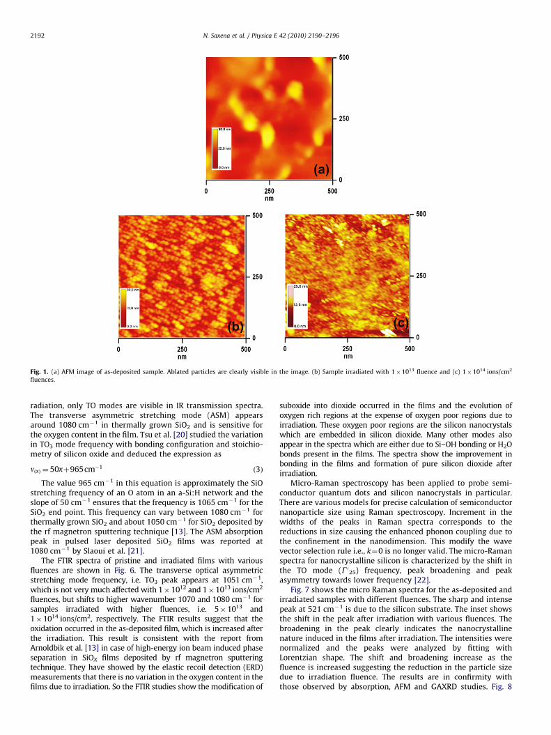
The atomic force microscopy (AFM) studies were carried out tomeasure the ablated particles’ size on the surface and to observe thesurface morphology of the films. Fig. 1 shows the AFM image ofseveral isolated laser ablated particles in the pristine sample andthose of the irradiated samples. It is clearly observed that theparticle size is decreased in the irradiated sample and it reducesfurther if the fluence is increased from 1�1013 to 1�1014 ions/cm2.Also some elongation of the particles is observed for the sampleirradiated with 1�1014 ions/cm2 fluence. The cluster size on the
surface was evaluated by the section analysis and it was found to be�35 nm in as-deposited sample while it showed �18 nm for thesample irradiated with 1�1013 ions/cm2 fluence and �15 nm forthe sample irradiated with 1�1014 ions/cm2 fluence. The reductionin size leads to the increment of the surface smoothness andreduction in the visibility of the particles.
The uniformity in size and smoothness of the surface isobserved in irradiated samples. This is clearly visible in the3-dimensional images of pristine and irradiated samples (Fig. 2).These images clearly show the change in the surface roughnessand the particle size on the surface of the samples. The surfaceroughness decreases drastically from 21.1 nm for pristine sampleto 4.3 nm for sample irradiated with 1�1013 ion/cm2 fluence and3.5 nm for sample irradiated with 1�1014 ion/cm2 fluence. Theseresults support the observed smoothening in the surface due toirradiation.
Fig. 3 shows the results of absorbance studies on the pristine aswell as irradiated samples. The as-deposited sample also showssome absorption edge due to the small particle size, while theirradiated samples show blue shift in absorption edge from295 nm for sample irradiated with 1�1013 ion/cm2 fluence to285 nm for sample irradiated with 1�1014 ions/cm2 fluence. Thisis due to the increased oscillator strength and exciton bindingenergy [18].
Tauc plot to evaluate the band gaps corresponding to theabsorbance in these samples is shown in Fig. 4. The calculatedband gaps are found to be 1.65, 2.19 and 2.64 eV for as-deposited,irradiated with 1�1013 and 1�1014 ions/cm2 fluences,respectively. The increased band gap in as-deposited sampleseems to be due to the presence of silicon oxide matrix whichreduces the silicon core. The increment in the band gap indicatesthe occurrence of quantum confinement in the as-grown sampleand further confinement due to reduction in crystal size inducedby irradiation. This is worthy to mention that this is an opticalband gap and it is always greater than the actual band gap. Herethe comparative study of band gap suggests the confinementoccurred in the nanocrystals.
Further to investigate the crystalline nature, the size reductionand phase of separated silicon, X-ray diffraction studies werecarried out on quartz substrate. This is shown in Fig. 5. The graphshows peaks at 28.41, 47.31 and 56.11 in the as-deposited film.These peaks are assigned for the (1 1 1), (2 2 0) and (3 1 1)orientations, respectively, in silicon cubic structure with cellparameter as 5.43 A [19]. The irradiated sample exhibits two extrapeaks at 38.11 and 44.21, which correspond to the (1 1 1) and(2 0 0) orientations of another cubic phase with lattice cellparameter as 3.9 A .The peak broadening in the XRD pattern ofsample irradiated with 1�1014 ions/cm2 fluence clearly suggeststhe reduction in the grain size and the formation of nanophase inthe film. The occurrence of another phase may be due to the factthat during phase separation silicon can be separated in a phasefor which cell parameter is smaller than 5.43 A corresponding tothe most common cubic phase. The grain size D is estimated usingDebye Scherrer’s formula, i.e.
D¼kl
b cosy, ð2Þ
where k is 0.9 for silicon, l the wavelength of Cu Ka radiation i.e.1.54 A, b the FWHM of the diffraction peak and y the diffractionangle. The grain size was found as �29 nm for as-grown film and�10 nm for the film irradiated with 1�1014 ions/cm2 fluence.This result is in agreement with AFM studies.
Fourier transform infrared spectroscopy gives informationabout the chemical modification of the silicon suboxide films. Itshows LO–TO split features of different TO vibrational modes.Since LO modes are optically weak for normal incidence of IR
ARTICLE IN PRESS
Fig. 1. (a) AFM image of as-deposited sample. Ablated particles are clearly visible in the image. (b) Sample irradiated with 1�1013 fluence and (c) 1�1014 ions/cm2
fluences.
N. Saxena et al. / Physica E 42 (2010) 2190–21962192
radiation, only TO modes are visible in IR transmission spectra.The transverse asymmetric stretching mode (ASM) appearsaround 1080 cm�1 in thermally grown SiO2 and is sensitive forthe oxygen content in the film. Tsu et al. [20] studied the variationin TO3 mode frequency with bonding configuration and stoichio-metry of silicon oxide and deduced the expression as
nðxÞ ¼ 50xþ965cm�1 ð3Þ
The value 965 cm�1 in this equation is approximately the SiOstretching frequency of an O atom in an a-Si:H network and theslope of 50 cm�1 ensures that the frequency is 1065 cm�1 for theSiO2 end point. This frequency can vary between 1080 cm�1 forthermally grown SiO2 and about 1050 cm�1 for SiO2 deposited bythe rf magnetron sputtering technique [13]. The ASM absorptionpeak in pulsed laser deposited SiO2 films was reported at1080 cm�1 by Slaoui et al. [21].
The FTIR spectra of pristine and irradiated films with variousfluences are shown in Fig. 6. The transverse optical asymmetricstretching mode frequency, i.e. TO3 peak appears at 1051 cm�1,which is not very much affected with 1�1012 and 1�1013 ions/cm2
fluences, but shifts to higher wavenumber 1070 and 1080 cm�1 forsamples irradiated with higher fluences, i.e. 5�1013 and1�1014 ions/cm2, respectively. The FTIR results suggest that theoxidation occurred in the as-deposited film, which is increased afterthe irradiation. This result is consistent with the report fromArnoldbik et al. [13] in case of high-energy ion beam induced phaseseparation in SiOX films deposited by rf magnetron sputteringtechnique. They have showed by the elastic recoil detection (ERD)measurements that there is no variation in the oxygen content in thefilms due to irradiation. So the FTIR studies show the modification of
suboxide into dioxide occurred in the films and the evolution ofoxygen rich regions at the expense of oxygen poor regions due toirradiation. These oxygen poor regions are the silicon nanocrystalswhich are embedded in silicon dioxide. Many other modes alsoappear in the spectra which are either due to Si–OH bonding or H2Obonds present in the films. The spectra show the improvement inbonding in the films and formation of pure silicon dioxide afterirradiation.
Micro-Raman spectroscopy has been applied to probe semi-conductor quantum dots and silicon nanocrystals in particular.There are various models for precise calculation of semiconductornanoparticle size using Raman spectroscopy. Increment in thewidths of the peaks in Raman spectra corresponds to thereductions in size causing the enhanced phonon coupling due tothe confinement in the nanodimension. This modify the wavevector selection rule i.e., k¼0 is no longer valid. The micro-Ramanspectra for nanocrystalline silicon is characterized by the shift inthe TO mode (G025) frequency, peak broadening and peakasymmetry towards lower frequency [22].
Fig. 7 shows the micro Raman spectra for the as-deposited andirradiated samples with different fluences. The sharp and intensepeak at 521 cm�1 is due to the silicon substrate. The inset showsthe shift in the peak after irradiation with various fluences. Thebroadening in the peak clearly indicates the nanocrystallinenature induced in the films after irradiation. The intensities werenormalized and the peaks were analyzed by fitting withLorentzian shape. The shift and broadening increase as thefluence is increased suggesting the reduction in the particle sizedue to irradiation fluence. The results are in confirmity withthose observed by absorption, AFM and GAXRD studies. Fig. 8

ARTICLE IN PRESS
Fig. 2. Three-dimensional AFM image of (a) pristine (b) irradiated with 1�1013 and (c) 1�1014 ions/cm2 fluences.
Fig. 3. UV–vis absorption spectra of (a) as-deposited (b) irradiated with 1�1013
and (c) 1�1014 ions/cm2 fluences.
Fig. 4. Tauc plot for the calculation of band gaps of (a) as-deposited sample
(b) irradiated with and (c) 1�1014 ions/cm2 fluences.
N. Saxena et al. / Physica E 42 (2010) 2190–2196 2193
shows the plot of the shift in the position of centroid and FWHMof Raman line shape with fluence. Though the shift is very smallsince the peak is dominated by the substrate but a careful analysisof the broadening suggests that the ion beam reduces the sizevery minutely and precise size selection is possible.
We have followed the spatial confinement model [23] forsilicon nanocrystals using the sinc weighting function andmodified integration limits. The first-order Raman spectra for
spherical nanocrystals is given by
IðoÞpX
n
Z ðnpþ1=DÞ
ðnp�1=DÞ
C2n ðqÞdq
½o�o0ðqÞ�2þðG=2Þ2ð4Þ
where
CnðqÞ ¼3sinðqD=2Þ
qp3D3ðk2n�q2Þ
ð5Þ

ARTICLE IN PRESS
Fig. 5. XRD pattern of as-grown sample and the sample irradiated with
1�1014 ions/cm2 fluence on quartz substrate.
Fig. 6. FTIR spectra of as-deposited and irradiated films.
Fig. 7. Micro-Raman spectra of pristine and irradiated films with indicated
fluences.
Fig. 8. Plot of Raman frequency shift and FWHM of Raman line with various
fluences.
Table 1Particle size calculated for different fluences by Raman spectroscopy.
Sample Particle size (nm)
Irradiated at 1�1012 ions/cm2 fluence 5.0
Irradiated at 1�1013 ions/cm2 fluence 4.3
Irradiated at 5�1013 ions/cm2 fluence 3.4
Irradiated at 1�1014 ions/cm2 fluence 3.2
N. Saxena et al. / Physica E 42 (2010) 2190–21962194
with kn¼np/D, n¼2,4,6, y, nmax (nmax is equal to the maximuminteger smaller than 2D/a), G is the Lorentzian line shapeand the phonon dispersion curve [o0(q)]2 adopts the analyticalform of
½o0ðqÞ�2 ¼ AþBcosðaq=4Þ ð6Þ
with q in the range of 0 and 2p/a, A¼1.714�105 cm�1 andB¼1.00�105 cm�1 as calculated from the neutron scatteringdata [24]. The sizes of the nanocrystals were calculated for variousfluences using this model and are given in Table 1.
4. Discussion
4.1. Role of spinodal decomposition in the growth of nanocrystals by
phase separation
The phase separation of pulsed laser ablated SiOX films andformation of silicon nanocrystals can be understood by invoking thetwo models: (i) continuous random body network model [25] and(ii) random mixing model [26]. As a continuous random bodynetwork, the silicon suboxide contains silicon tetrahedral with acentral silicon atom bonded to four Si and/or O atoms. The propertyof this suboxide to transit from one form to another by the reductionin one silicon atom along with the oxidation of the nearest onemakes this system to fulfill the condition of spinodal decomposition.The random network of the suboxide attributes some penaltyenergy, which is the excess energy of the system due to the presenceof different oxidation states of silicon. Hence, it follows that thesuboxide is unstable against the decomposition into two phases, i.e.Si0 and Si+4, which are the spinodal points as calculated by Barrancoet al. [27], though Hamann [28] calculated it as Si0 and Si+3.According to random mixing model, it is supposed that the twophases, i.e. higher concentration and lower concentration arerandomly distributed, which are enriched in the process of phaseseparation, e.g. silicon rich region becomes more silicon rich andsilicon poor region becomes more silicon poor. In order to under-stand the spinodal decomposition in silicon oxide, we assume thatthe concentration of the two constituents A and B in the binary

ARTICLE IN PRESS
N. Saxena et al. / Physica E 42 (2010) 2190–2196 2195
solution AB is XA and XB, respectively. If G0A and G0
Bdesignate the freeenthalpies of pure substances A and B, respectively, we can takeG(XA, XB) as the free enthalpy of the solution
G¼ XAG0AþXBG0
BþuXAXBþRT½XA lnXAþXB lnXB� ð7Þ
R is the ideal gas constant. In this equation, it was assumed that theenergy of interaction between constituents A and B in the mixture isproportional to the product of their concentrations (the term uXAXB).The energy of interaction can take this form only if it is assumedthat: (1) the molecules in the solution are positioned next to eachother so that each molecule has the same number of near neighbors,this is called a lattice model (as stated by the continuous bodynetwork model for SiOX); (2) the mixture is totally random (as statedby the random mixing model for SiOX) and (3) the intermolecularforces are of short range and that only the binary interactionsbetween closest neighbors can be taken into consideration.The fourth term in the above equation represents the contributionof the entropy of mixing to G(XA, XB). A solution in which the freeenthalpy is given by the above equation is called a regular solution.The behavior of the solution, specially the metastability limit, can beinvestigated by the above equation using the condition formetastability, i.e.
d2G¼ 0 ð8Þ
Assuming X¼XA with XA+XB¼1, the equation is rewritten as
G¼ XG0Aþð1�XÞG0
BþuXð1�XÞþRT X lnXþð1�XÞlnð1�XÞ� �
ð9Þ
Condition (8) leads to the equation
�2uXð1�XÞþRT ¼ 0 ð10Þ
This equation represents a curve, which gives the shape of thespinodal (Fig. 9). The spinodal curve demarcates the metastabilitylimit and shares the critical point with the coexistence curve.
The spinodal decomposition takes place when the mixture is ina region of thermodynamical instability but is still homogeneous.This is the site of local and spontaneous fluctuations in theconcentration C, which are the source of inhomogeneity withinthe mixture. Two different phenomena take place depending onthe state of mixture. If the mixture is in unstable region, theconcentration will vary uniformly and continuously in space andtime until the new phase is formed and if the mixture is in meta-stable state, there are important concentration discontinuitiescorresponding to the appearance of nuclei of the new phase at the
Fig. 9. Schematic phase diagram of a binary solution with a miscibility gap below
the critical temperature TC. The mixture becomes unstable inside the spinodal:
there is phase separation.
beginning of the transformation. In other words, there arehomogeneous concentration fluctuations in the case of spinodaldecomposition and heterogeneous fluctuations in the case of thetransition by nucleation.
4.2. Role of swift heavy ions in the growth and size tuning of
nanocrystals
The dominant mechanism for a highly charged ion moving at avelocity comparable to the Bohr velocity of the electron is theinelastic collision leading to dense ionization and excitation ofatoms around the trajectory. Swift heavy ions (SHI) deposit a hugeamount of energy (� keV/nm) uniformly throughout the thick-ness of the film for producing latent tracks of nanometer sizewhen its value crosses the threshold value for track formation,which alters the properties of the film as well as the nanos-tructures therein. During a very short time of femtosecond (fs)after the swift heavy ion passes, the ensemble of excited electronsin the vicinity of the ion trajectory is thermalized. This increasesthe local electronic temperature spike to �105 K. A thermal spikeresults due to the energy transfer from the excited electrons totarget atoms. The electronic temperature then decreases viaelectron heat conduction into the surrounding matrix and via heatexchange with the lattice. The ionic temperature profile isdissipated in a time of the order of nanoseconds (10�9 s).
Thus the ion beam induced thermal spike causes localized (nm)annealing, which results in the phase separation of the siliconsuboxide formed during pulsed laser ablation of silicon in oxygenenvironment. This suboxide fulfills the condition for spinodaldecomposition and when the local inhomogeneities in theconcentration are activated in non equilibrium condition by swiftheavy ion beam irradiation, it undergoes the phase separation. Thisphase separation leads to enrichment of silicon rich and silicon poorregions in the film. Silicon rich regions become more silicon richand silicon poor regions become more silicon poor in the track andthe formation of silicon nanocrystals takes place. Increase in the ionfluence results in smaller particles and increase in the surfacesmoothness. This is due to the fact that more number of ionsproduce more number of latent tracks in the same volume of thefilm causing more spinodal decomposition. The formation ofanother phase with less cell parameter is possible due to the factthat in phase separation silicon can grow in any phase and withdifferent lattice parameters as reported in this work.
5. Conclusion
Swift heavy ion (SHI) beam is found to be an important tool tosynthesize chemically pure and stable nanoparticles in aninsulating matrix. Electronic excitation induced by the SHI beamis able to enhance the phase separation in a solution with localfluctuations. The blue-shift of the absorption edge as well as theband gap energies for samples which are irradiated indicatethe decrease in silicon nanocrystal size due to the confinement ofthe nanosized precipitates inside the track. It is found that the sizeof the silicon nanocrystals can be tuned by ion beam in acontrolled manner in pulsed laser ablated films of silicon oxide.
Acknowledgments
One of the authors (NS) is thankful to Inter University AcceleratorCenter for providing funds in terms of fellowship and ion beamfacility to carry out this work. The help received from Dr. YashpalKatharia, Dr. Ambuj Tripathi and UGC-DAE Consortium for ScientificResearch, Indore, is gratefully acknowledged.

ARTICLE IN PRESS
N. Saxena et al. / Physica E 42 (2010) 2190–21962196
References
[1] L.T. Canham, Appl. Phys. Lett. 57 (10) (1990) 1046.[2] L. Pavesi, L. Dal Negro, C. Mazzoleni, G. Franzo, F. Priolo, Nature 408 (2000)
440.[3] A.J. Kenyon, P.F. Trwoga, C.W. Pitt, J. Appl. Phys. 79 (12) (1996) 9291.[4] X.Y. Chen, Y.F. Lu, L.J. Tang, Y.H. Wu, B.J. Cho, X.J. Xu, J.R. Dong, W.D. Song,
J. Appl. Phys. 97 (2005) 014913.[5] E. Fazio, E. Barletta, F. Barreca, F. Neri, S. Trusso, J. Vac. Sci. Technol. B 23 (2)
(2005) 519.[6] D. Riabinina, C. Durand, M. Chaker, F. Rosei, Appl. Phys. Lett. 88 (2006)
073105.[7] H.Z. Song, X.M. Bao, N.S. Li, X.L. Wu, Appl. Phys. Lett. 72 (3) (1998) 356.[8] D.J. Lockwood, Z.H. Lu, J.M. Baribeau, Phys. Rev. Lett. 76 (3) (1996) 539.[9] M. Benyoucef, M. Kuball, J.M. Sun, G.Z. Zhong, X.W. Fan, J. Appl. Phys. 89 (12)
(2001) 7903.[10] S. Yerci, U. Serincan, I. Dogan, S. Tokay, M. Genisel, A. Aydinli, R. Turan, J. Appl.
Phys. 100 (2006) 074301.[11] T. Mohanty, A. Pradhan, S. Gupta, D. Kanjilal, Nanotechnology 15 (2004) 1620.[12] P.S. Choudhary, T.M. Bhave, D. Kanjilal, S.V. Bhoraskar, J. Appl. Phys. 93 (6)
(2003) 3486.
[13] W.M. Arnoldbik, N. Tomozeiu, E.D. van Hattum, R.W. Lof, A.M. Verdenberg,F.H.P.M. Habraken, Phys. Rev. B 71 (2005) 125329.
[14] L. Patrone, D. Nelson, V.I. Safarov, M. Sentis, W. Marine, S. Giorgio, J. Appl.Phys. 87 (8) (2000) 3829.
[15] E. van de Riet, C.J.C.M. Nillesen, J. Dieleman, J. Appl. Phys. 74 (1993) 2008.[16] D. Kanjilal, S. Chopra, M.M. Narayanan, I.S. Iyer, V. Jha, R. Joshi, S.K. DattaNucl.
Instrum. Methods A 328 (1–2) (1993) 97.[17] www.srim.org.[18] Z. Xinwei, S. Olaf, K. Shuji, A. Yoshinobu, S. Takuo, Phys. Rev. B50 (1994)
18654.[19] X-ray powder Diffraction, JCPDS—International Center for Diffraction Data,
USA, 1999.[20] D.V. Tsu, G. Lucovsky, B.N. Davidson, Phys. Rev. B40 (3) (1989) 1795.[21] A. Slaoui, E. Fogarassy, C. Fuchs, P. Siffert, J. Appl. Phys. 71 (2) (1992) 590.[22] W. Zhang, S. Zhang, Y. Liu, T. Chen, J. Cryst. Growth 311 (2009) 1296.[23] G. Faraci, S. Gibilisco, P. Russo, A.R. Pennisi, Phys. Rev. B73 (2006) 033307.[24] R. Tubina, L. Piseri, G. Zerbi, J. Chem. Phys. 56 (3) (1972) 1022.[25] F.G. Bell, L. Ley, Phys. Rev. B37 (14) (1988) 8383.[26] H. Watanabe, K. Haga, T. Lohner, J. Non-Cryst. Sol. 164–166 (1993) 1085.[27] A. Barranco, J.A. Mejias, J.P. Espinnos, A. Cabellero, A.R. Gonzalez-Elipe
F. Yubero, J. Vac. Sci. Technol. A19 (2001) 136.[28] D.R. Hamann, Phys. Rev. B61 (15) (2000) 9899.