controlnet applications with the sn65hvd61 phy … · application report slla265a–september...
TRANSCRIPT

Application ReportSLLA265A–September 2007–Revised September 2008
ControlNet™ Applications With the SN65HVD61 PHYClark Kinnaird ......................................................................................................... Industrial Interface
ABSTRACTThis application note is a guide for using the SN65HVD61 physical layer transceiver(PHY) for ControlNet industrial data communications network applications. Designersfamiliar with existing ControlNet PHY implementations will find guidance for convertingto the SN65HVD61, which offers cost-effective improvements in board space, powerconsumption, and robustness. In addition to advice for drop-in replacement, we alsopresent suggestions for taking advantage of the new features of the SN65HVD61(hereafter also referred to as the HVD61), including low-voltage MAC interface, signaldiagnostics, and enable/disable functions.
Contents1 Introduction to ControlNet ......................................................................... 2
1.1 Overview .................................................................................... 21.2 Physical Layer ............................................................................. 3
2 The SN65HVD61 ControlNet PHY ............................................................... 32.1 Circuit Placement with MAC and Transformer......................................... 32.2 Block Diagram of the HVD61 ............................................................ 4
3 Replacing the Hybrid Module With the HVD61 ................................................. 53.1 Compatibility With Existing Solutions ................................................... 63.2 Single-Channel Application............................................................... 93.3 Dual-Channel Application ............................................................... 11
4 Next-Generation Design With the SN65HVD61............................................... 134.1 Improved Characteristics................................................................ 134.2 New Functions............................................................................ 154.3 CHIP ENABLE Function................................................................. 16
5 More Information .................................................................................. 165.1 Example Implementations .............................................................. 16
6 Conclusion ......................................................................................... 17
List of Figures
1 ControlNet Applications ............................................................................ 32 HVD61 PHY Connects the MAC to the ControlNet Bus....................................... 33 HVD61 Block Diagram ............................................................................. 44 Hybrid Package (Single Channel) ................................................................ 55 SN65HVD61 Package (Single Channel) ........................................................ 56 Transmitted Signal Levels ......................................................................... 67 Test Set-up Demonstrates Interoperability of Old and New Transceivers .................. 78 Hybrid and Hybrid Communication ............................................................... 89 SN65HVD61 and Hybrid Communication ....................................................... 810 Hybrid and Hybrid Communication – Trigger on Node 1...................................... 811 SN65HVD61 and Hybrid Communication – Trigger on Node 1 .............................. 812 Hybrid and Hybrid Communication – Trigger on Node 2...................................... 913 SN65HVD61 and Hybrid Communication – Trigger on Node 2 .............................. 914 Schematic for Direct Replacement in Single-Channel Application ......................... 10
ControlNet is a trademark of ODVA.Rockwell Automation, Allen Bradley are registered trademarks of Rockwell Automation, Inc..
SLLA265A–September 2007–Revised September 2008 ControlNet™ Applications With the SN65HVD61 PHY 1Submit Documentation Feedback
1 Introduction to ControlNet
1.1 Overview
Introduction to ControlNet www.ti.com
15 Dual-Channel SIP Hybrid SN65HVD61 Implementation..................................... 1216 Simplified Test Set-up for EMC Standards .................................................... 1417 Nominal Transfer Function of the SN65HVD61 SIG Feature ............................... 1518 Differential Input (Ch.1) and SIG Output (Ch.2)............................................... 1619 Engineering Prototype SN65HVD61-to-Hybrid Replacement ............................... 1720 Example SN65HVD61-to-Hybrid Replacement Printed Circuit Board ..................... 17
List of Tables
1 Components Used in Interoperability Demonstration .......................................... 72 SN65HVD61 Pin Assignments for Direct Replacement of a Single-Channel Hybrid ..... 93 SN65HVD61 Pin Assignments for Direct Replacement of a Dual-Channel Hybrid ...... 114 Power Supply Requirements .................................................................... 135 EMC Standards ................................................................................... 14
ControlNet is an open standard network that meets the demands of industrial applications requiring highspeed (5 Megabits per second), high throughput with predictable and repeatable transfers of missioncritical data.
ControlNet is one of the network technologies that comprise the family of networks built on the CommonIndustrial Protocol. ControlNet meets the demands of real-time, high speed applications at the automationand control layer for integration of complex control systems such as coordinated drive systems, weldcontrol, motion control, vision systems, complex batch control systems, process control systems with largedata requirements, and systems with multiple controllers and human-machine interfaces. ControlNet iseffective for systems with multiple PC-based controllers and Programmable Logic Controller (PLC)-to-PLCand PLC-to-Digital Control System (DCS) communication. ControlNet allows multiple controllers – eachwith their own I/O and shared inputs – to talk to each other, with any possible interlocking combination.
ControlNet can be implemented on several different types of media, including copper coax cable, fiberoptic cable, and fiber ring, with variations for media redundancy and intrinsically-safe applications. In thisapplication note, the discussion is limited to copper coax cable implementations.
ControlNet supports a maximum of 99 nodes, with no minimum distance limitation between nodes. Itoffers high network efficiency with multicast of inputs and peer-to-peer data, using a Producer/Consumercommunication model that allows the user to configure devices, control actions, and collect informationover a single network
More information about ControlNet can be obtained from the ControlNet International website:http://www.odva.org
ControlNet™ Applications With the SN65HVD61 PHY2 SLLA265A–September 2007–Revised September 2008Submit Documentation Feedback

1.2 Physical Layer
VCC
75 W 75 W
HVD61 HVD61HVD61
1:1:1 XFRM
PASSIVETAP
(ImpedanceMatching)
PASSIVETAP
(ImpedanceMatching)
PASSIVETAP
(ImpedanceMatching)
VCC VCC
2 The SN65HVD61 ControlNet PHY
2.1 Circuit Placement with MAC and Transformer
ControlNet
MAC HVD61
TXEN
CHEN
CD
TX
TXBAR
RX
ControlNet Bus
SIG
VCC
www.ti.com The SN65HVD61 ControlNet PHY
ControlNet's coax media specifies RG-6 quad shield cable, which is relatively inexpensive and usedwidely in the cable TV industry. The standard provides support for bus, star, or tree topologies to meetvarious application needs. Passive taps can be installed anywhere on the trunk with no minimum spacingrequirements.
In a typical ControlNet application, several nodes will be connected to a common bus, as shown inFigure 1. At any time, only one node should drive the bus; all active nodes continually receive the busstate. The node, which is actively driving the bus, will sink current through one of the HVD61 drivers,causing the voltage on the bus to be either differential high or differential low.
Figure 1. ControlNet Applications
The SN65HVD61 transceiver is a mixed-signal (digital and analog) device that translates the logic signalsbetween the Media Access Controller (MAC) and the ControlNet bus lines. The logic signals to and fromthe MAC are compatible with TTL, LVTTL, or CMOS logic levels. The XF1 and XF3 pins (see Figure 3)are designed to connect with a pulse transformer as specified by the ControlNet specification.
Figure 2 shows the connections between the MAC and the HVD61. For simplicity, power supplyconnections and external protection components are not shown.
Figure 2. HVD61 PHY Connects the MAC to the ControlNet Bus
SLLA265A–September 2007–Revised September 2008 ControlNet™ Applications With the SN65HVD61 PHY 3Submit Documentation Feedback

2.2 Block Diagram of the HVD61
RX
CD
XF1
XF3
TXEN
TX
TX
CGND
VCC
CHEN
TSD
SIG 0.1
DGND
VDD
14
2
3
4
5
6
7
8
9
10
11,13
12
_+
_+
1
The SN65HVD61 ControlNet PHY www.ti.com
Figure 3 shows a block diagram of the HVD61 ControlNet transceiver. Each of the functional blocks isimplemented in proven Linear BiCMOS process technology. The transceiver is packaged in a standard14-pin small-outline integrated circuit (SOIC). Full specifications for the performance and operatingconditions of the HVD61 are detailed in the SN65HVD61 datasheet available at www.ti.com.
Figure 3. HVD61 Block Diagram
ControlNet™ Applications With the SN65HVD61 PHY4 SLLA265A–September 2007–Revised September 2008Submit Documentation Feedback

3 Replacing the Hybrid Module With the HVD61
1 2 3 4 6 7 8 9 10 11 12
35.5 mm
13.2 mm
28 mm
2.5 mm
ALLEN-BRADLEY
www.ti.com Replacing the Hybrid Module With the HVD61
Rockwell Automation® (formerly Allen Bradley®) has supplied single-channel and dual-channel ControlNettransceivers for several years. Each hybrid transceiver module implements the requirements of a coaxtransceiver when combined with a transformer and certain external components for electromagneticcompatibility. The hybrid transceiver functionally replaces about 50 discrete surface-mount components, ina Single-In-line Package (SIP) as shown in Figure 4.
Figure 4. Hybrid Package (Single Channel)
Figure 5. SN65HVD61 Package (Single Channel)
SLLA265A–September 2007–Revised September 2008 ControlNet™ Applications With the SN65HVD61 PHY 5Submit Documentation Feedback
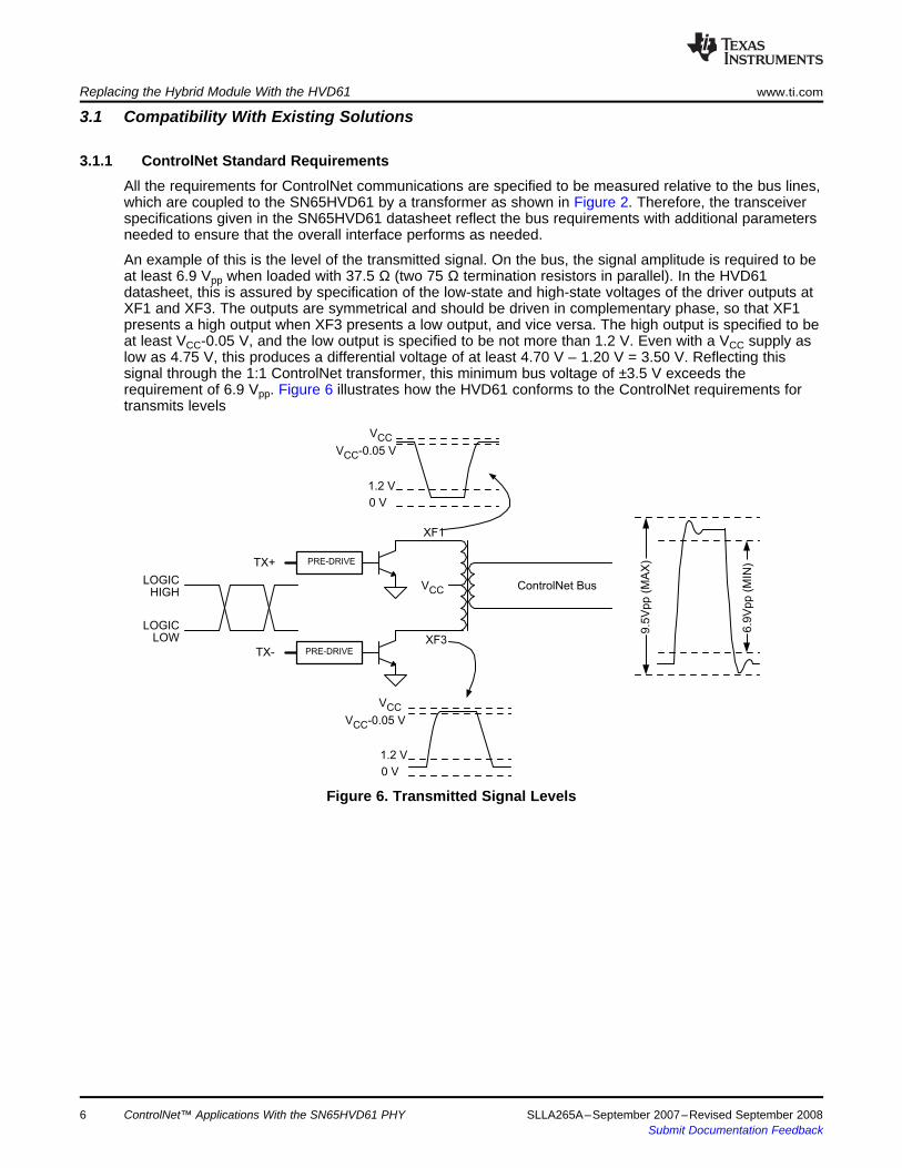
3.1 Compatibility With Existing Solutions
3.1.1 ControlNet Standard Requirements
ControlNet BusVCC
TX+
TX- PRE-DRIVE
XF1
XF3
LOGICLOW
LOGICHIGH
1.2 V
0 V
VCC
V -0.05 VCC
1.2 V
0 V
9.5
Vp
p (
MA
X)
6.9
Vp
p (
MIN
)
VCC
V -0.05 VCC
PRE-DRIVE
Replacing the Hybrid Module With the HVD61 www.ti.com
All the requirements for ControlNet communications are specified to be measured relative to the bus lines,which are coupled to the SN65HVD61 by a transformer as shown in Figure 2. Therefore, the transceiverspecifications given in the SN65HVD61 datasheet reflect the bus requirements with additional parametersneeded to ensure that the overall interface performs as needed.
An example of this is the level of the transmitted signal. On the bus, the signal amplitude is required to beat least 6.9 Vpp when loaded with 37.5 Ω (two 75 Ω termination resistors in parallel). In the HVD61datasheet, this is assured by specification of the low-state and high-state voltages of the driver outputs atXF1 and XF3. The outputs are symmetrical and should be driven in complementary phase, so that XF1presents a high output when XF3 presents a low output, and vice versa. The high output is specified to beat least VCC-0.05 V, and the low output is specified to be not more than 1.2 V. Even with a VCC supply aslow as 4.75 V, this produces a differential voltage of at least 4.70 V – 1.20 V = 3.50 V. Reflecting thissignal through the 1:1 ControlNet transformer, this minimum bus voltage of ±3.5 V exceeds therequirement of 6.9 Vpp. Figure 6 illustrates how the HVD61 conforms to the ControlNet requirements fortransmits levels
Figure 6. Transmitted Signal Levels
ControlNet™ Applications With the SN65HVD61 PHY6 SLLA265A–September 2007–Revised September 2008Submit Documentation Feedback

3.1.2 Similarity to Hybrid Characteristics
NODE 1
COMM.
BRIDGE
TAPR TAP
NODE 2
COMM.
BRIDGE
T T
OSCILLOSCOPE
TRIGGERBUS
CHECKER
10 METER CABLER
www.ti.com Replacing the Hybrid Module With the HVD61
The design of the HVD61 is such that a ControlNet node using the HVD61 has performance that matchesthe characteristics of nodes using the existing hybrid transceiver in all critical parameters. This assuresinteroperability of networks with mixed old and new types of transceivers. This also assures compatibilityof the HVD61 for applications replacing the existing hybrid transceiver.
To demonstrate interoperability between the HVD61 and hybrid transceivers, the test set-up shown inFigure 7 was used to observe typical bus signal data. Standard ControlNet components were used toillustrate a simple application.
Figure 7. Test Set-up Demonstrates Interoperability of Old and New Transceivers
Table 1. Components Used in Interoperability DemonstrationMANUFACTURER DESCRIPTION PART NUMBER QUANTITYAllen-Bradley ControlNet Communications Bridge 1756-CNBR/D 2Allen-Bradley ControlLogix Power Supply 1756-PA72/B 1Allen-Bradley ControlLogix 4-Slot Chassis 1756-A4/A 1Allen-Bradley Passive Tap 1786 TPR/B 2
75 Ω Coax Terminator 2Belden Quad Shield ControlNet Cable 3092A 10 metersAllen-Bradley Net Checker 1788 CNCHR/A 1
The following figures show oscilloscope traces of bus activity with two nodes communicating. In each pairof figures, the first figure shows two hybrid (old) transceivers communicating, and the second figure showsone SN65HVD61 (new) and one hybrid (old) transceiver communicating. Note that there is no noticeabledifference in the signaling between the two different combinations.
SLLA265A–September 2007–Revised September 2008 ControlNet™ Applications With the SN65HVD61 PHY 7Submit Documentation Feedback

Replacing the Hybrid Module With the HVD61 www.ti.com
In Figure 8 and Figure 9, we see two bursts of communication signals, one from Node 1 at the near end ofthe cable, and one from Node 2 at the far end of the cable. No particular details are intended, but thesetraces give an overview for the total communications sequence. The blue (top) trace in both figures is thesynchronization trigger signal from the bus checker. This trigger signal can be used to select either Node 1or Node 2 for the more detailed traces to follow.
Figure 9. SN65HVD61 and HybridFigure 8. Hybrid and Hybrid CommunicationCommunication
In Figure 10 and Figure 11, the synchronization trigger is set for Node 1. The bus signal trace shows thecharacteristics of amplitude (>6.9 Vpp) and bit width (either 100 ns or 200 ns depending on Manchestercode symbol) that are appropriate for ControlNet signaling.
Figure 10. Hybrid and Hybrid Communication Figure 11. SN65HVD61 and Hybrid– Trigger on Node 1 Communication – Trigger on Node 1
8 ControlNet™ Applications With the SN65HVD61 PHY SLLA265A–September 2007–Revised September 2008Submit Documentation Feedback
3.2 Single-Channel Application
www.ti.com Replacing the Hybrid Module With the HVD61
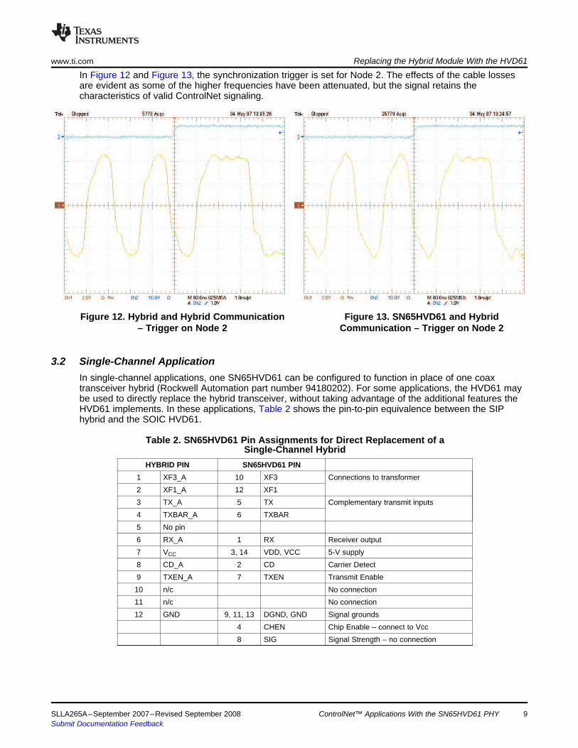
In Figure 12 and Figure 13, the synchronization trigger is set for Node 2. The effects of the cable lossesare evident as some of the higher frequencies have been attenuated, but the signal retains thecharacteristics of valid ControlNet signaling.
Figure 12. Hybrid and Hybrid Communication Figure 13. SN65HVD61 and Hybrid– Trigger on Node 2 Communication – Trigger on Node 2
In single-channel applications, one SN65HVD61 can be configured to function in place of one coaxtransceiver hybrid (Rockwell Automation part number 94180202). For some applications, the HVD61 maybe used to directly replace the hybrid transceiver, without taking advantage of the additional features theHVD61 implements. In these applications, Table 2 shows the pin-to-pin equivalence between the SIPhybrid and the SOIC HVD61.
Table 2. SN65HVD61 Pin Assignments for Direct Replacement of aSingle-Channel Hybrid
HYBRID PIN SN65HVD61 PIN1 XF3_A 10 XF3 Connections to transformer2 XF1_A 12 XF13 TX_A 5 TX Complementary transmit inputs4 TXBAR_A 6 TXBAR5 No pin6 RX_A 1 RX Receiver output7 VCC 3, 14 VDD, VCC 5-V supply8 CD_A 2 CD Carrier Detect9 TXEN_A 7 TXEN Transmit Enable10 n/c No connection11 n/c No connection12 GND 9, 11, 13 DGND, GND Signal grounds
4 CHEN Chip Enable – connect to Vcc8 SIG Signal Strength – no connection
SLLA265A–September 2007–Revised September 2008 ControlNet™ Applications With the SN65HVD61 PHY 9Submit Documentation Feedback

3.2.1 External Components
5 V
SN65HVD61
1:1:1 XFRM
30 V
MOV1M 0.01 Fm
XF1
XF3
2.2 nF10 Fm
5 V
RX
CD
TX
TXEN
TX
10 Fm
16 V
0.1 Fm
25 V
1
2
5
6
7 10
12
3, 14
9, 11, 13
5 V 4
Replacing the Hybrid Module With the HVD61 www.ti.com
Note that in these direct-replacement applications, both supply lines (Vcc and VDD) should be tied to asingle 5-V supply. Also, all ground pins (DGND and both CGND pins) should be tied to the common signalground
In order to achieve system-level performance similar to the hybrid transceiver, applications replacing thehybrid with the HVD61 should use the same external components as in previous designs. These externalcomponents include decoupling capacitors on the power supply and protection devices on the bus signals.
During system-level testing with the HVD61, external components were used as suggested by RockwellAutomation, as shown in Figure 14.
Figure 14. Schematic for Direct Replacement in Single-Channel Application
The 1:1:1 pulse transformer is described by the ControlNet specification, and may be available fromRockwell Automation. EPCOS (www.epcos.com) also provides a transformer suitable for ControlNetapplications; this is series T4312 with ordering code B78417P8441A005.
The 30-V MOV acts to reduce transient surge voltages. Rockwell Automation in the past has suggestedthe Harris part number V30MLA1812TX1884 to help pass surge testing. Littelfuse (www.littelfuse.com)makes a family of multilayer transient voltage suppressors, which may have similar characteristics to theHarris part.
The 2.2 nF (2200 pF) capacitor shown in the circuit is optional, and is intended to improve electromagneticcompatibility performance at the systems level. This capacitor is connected across the transformer fromthe primary to the secondary, between VCC on the chip side and chassis ground on the bus side. Since theisolation rating on the transformer is 500 Vac rms, the capacitor should have a voltage rating of at least500 Vac.
ControlNet™ Applications With the SN65HVD61 PHY10 SLLA265A–September 2007–Revised September 2008Submit Documentation Feedback

3.3 Dual-Channel Application
3.3.1 Pin-to-Pin Assignment
www.ti.com Replacing the Hybrid Module With the HVD61
In dual-channel (redundant) applications, two SN65HVD61 transceivers can be configured to function inplace of one coax dual transceiver hybrid (Rockwell Automation part number 94180201). For someapplications, the HVD61 devices may be used to directly replace the hybrid transceiver, without takingadvantage of the additional features the HVD61 implements. In these applications, the table below showsthe pin-to-pin equivalence between the SIP hybrid and the two SOIC HVD61 devices.
Table 3. SN65HVD61 Pin Assignments for Direct Replacement of a Dual-Channel HybridHYBRID PIN SN65HVD61 A PIN SN65HVD61 B PIN1 XF3_A 10 XF3 (A) Connections to transformer (A)2 XF1_A 12 XF1 (A)3 TX_A 5 TX (A) Complementary transmit inputs (A)4 TXBAR_A 6 TXBAR (A)5 No pin6 RX_A 1 RX (A) Receiver output (A)7 VCC 3, 14 3,14 VDD, VCC 5V supply8 CD_A 2 CD (A) Carrier Detect (A)9 TXEN_A 7 TXEN (A) Transmit Enable (A)10 TXEN_B 7 TXEN (B) Transmit Enable (B)11 RX_B 1 RX (B) Receiver output (B)12 GND 9, 11, 13 9,11,13 DGND, CGND Signal grounds13 CD_B 2 CD (B) Carrier Detect (B)14 TXBAR_B 6 TXBAR(B) Complementary transmit inputs (B)15 TX_B 5 TX (B)16 XF1_B 12 XF1 (B) Connections to transformer (B)17 XF1_B 10 XF3 (B)
4 4 CHEN Chip Enable – connect to Vcc8 8 SIG Signal Strength – make no connection
Note that in these direct-replacement applications, all supply lines (VCC and VDD) should be tied to asingle 5-V supply. Also, all ground pins (DGND and CGND pins) should be tied to the common signalground.
SLLA265A–September 2007–Revised September 2008 ControlNet™ Applications With the SN65HVD61 PHY 11Submit Documentation Feedback

3.3.2 External Components
Replacing the Hybrid Module With the HVD61 www.ti.com
For a dual-channel application, the same external protection and filtering components are suggested asfor the single-channel application. For simplicity, replicate the circuit shown in Figure 14 for each channel.Figure 15 shows an example implementation of a dual-channel application using two HVD61 devices on asingle single in-line package (SIP) board.
Figure 15. Dual-Channel SIP Hybrid SN65HVD61 Implementation
ControlNet™ Applications With the SN65HVD61 PHY12 SLLA265A–September 2007–Revised September 2008Submit Documentation Feedback

4 Next-Generation Design With the SN65HVD61
4.1 Improved Characteristics
4.1.1 1. Operating Temperature to 100°C
4.1.2 Lower Power Consumption
4.1.3 ESD Protection
4.1.3.1 Chip-Level ESD Protection
www.ti.com Next-Generation Design With the SN65HVD61
The HVD61 is characterized for operation over the temperature range of –40°C to 100°C. This givessystem designers more latitude compared to previous implementations, which were typically limited totemperature ranges of 0°C to 85°C. As with all designs, proper care must be taken to ensure that themaximum temperature of any device does not exceed the rated temperature. This involves understandingnot only the ambient temperature, but also the junction temperature rating and thermal design of theboard.
For more information regarding thermal constraints, see the ABSOLUTE MAXIMUM RATINGS table, theABSOLUTE MAXIMUM RATINGS table, and the THERMAL CHARACTERISTICS OF IC PACKAGESsection in the SN65HVD61 data sheet. A discussion of thermal modeling and junction temperaturecalculations is given in the Texas Instruments Applications Note IC Package Thermal Metrics (TI literaturenumber SPRA953).
The quiescent (transmitter off) supply current for hybrid implementations of the ControlNet transceiver isspecified as typically about 50 mA, and can vary to a maximum of almost 75 mA. Under similar conditionswith the chip disabled, the HVD61 supply current is specified as typically about 1.8 mA, with a maximumof 3 mA. This includes both the analog supply VCC and the digital supply VDD.
In dynamic operating conditions, the active supply current is much higher for both the hybrid-transceiverand the SN65HVD61 implementation. The load current is supplied through the center-tap of thetransformer, so this is not included as part of the transceiver supply current. The rms supply current to thehybrid transceiver can typically be as high as 180 mA; the analog rms supply current to the SN65HVD61is typically about 36 mA, and the digital supply less than 5 mA for a total of about 40 mA.
The load current on the bus is supplied by the 5 V on the bus transformer’s center-tap, independent ofwhich type of transceiver is used. Assuming that the bus is correctly terminated with 37.5 Ω (75 Ωimpedance at each end), and that the signaling levels meet the ControlNet requirements of ±4.1 V (8.2Vpp), a nominal current of 109 mA occurs when the transmitter is active. The maximum level of ±4.75 V(9.5 Vpp) corresponds to a load current of 127 mA.
Table 4. Power Supply RequirementsTransceiver VCC (5 V) VDD (2.5 V, 3.3 V, or 5 V) VCC (5 V) Transformer Total Power Supply Current
Hybrid (single) 200 mA Not applicable 130 mA 330 mASN65HVD61 65 mA 5 mA 130 mA 200 mA
Electrostatic discharges constitute a danger for all integrated circuits, including the SN65HVD61.Electrostatic charging can occur as a result of friction, such as when one walks on a carpet, causing thebody to become charged. If a conducting object such as a piece of equipment connected to a ground lineis touched, the body is discharged. The electrostatic energy stored as charge is injected into the objectthat is touched, and is converted primarily into heat. The power dissipation that arises in such cases candamage the electronic circuits.
Test circuits have been developed to test sensitivity to electrostatic discharges by simulating variousscenarios. These test circuits are analyzed in more detail in the following paragraphs. These shouldprovide the design engineer with insight into the protection circuits, and whether additional precautions arenecessary.
SLLA265A–September 2007–Revised September 2008 ControlNet™ Applications With the SN65HVD61 PHY 13Submit Documentation Feedback
4.1.3.2 Board-Level Protection
HVD61
1:1:1 XFRM
RG-6 Coax
30 V
MOV1M 0.01 Fm
XF1
XF3
2.2 nF 10 Fm
IEC stimuli applied here
VCC
Passive
Impedance-
Matching
TapVCC
Next-Generation Design With the SN65HVD61 www.ti.com
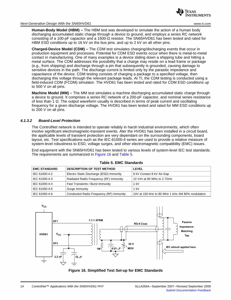
Human-Body Model (HBM) – The HBM test was developed to simulate the action of a human bodydischarging accumulated static charge through a device to ground, and employs a series RC networkconsisting of a 100-pF capacitor and a 1500-Ω resistor. The SN65HVD61 has been tested and rated forHBM ESD conditions up to 16 kV on the bus pins, and up to 2 kV on all other pins.
Charged-Device Model (CDM) – The CDM test simulates charging/discharging events that occur inproduction equipment and processes. Potential for CDM ESD events occur when there is metal-to-metalcontact in manufacturing. One of many examples is a device sliding down a shipping tube and hitting ametal surface. The CDM addresses the possibility that a charge may reside on a lead frame or package(e.g., from shipping) and discharge through a pin that subsequently is grounded, causing damage tosensitive devices in the path. The discharge current is limited only by the parasitic impedance andcapacitance of the device. CDM testing consists of charging a package to a specified voltage, thendischarging this voltage through the relevant package leads. At TI, the CDM testing is conducted using afield-induced CDM (FCDM) simulator. The HVD61 has been tested and rated for CDM ESD conditions upto 500 V on all pins.
Machine Model (MM) – The MM test simulates a machine discharging accumulated static charge througha device to ground. It comprises a series RC network of a 200-pF capacitor, and nominal series resistanceof less than 1 Ω. The output waveform usually is described in terms of peak current and oscillatingfrequency for a given discharge voltage. The HVD61 has been tested and rated for MM ESD conditions upto 200 V on all pins.
The ControlNet network is intended to operate reliably in harsh industrial environments, which ofteninvolve significant electromagnetic-transient events. Ater the HVD61 has been installed in a circuit board,the applicable levels of transient protection are very dependant on the surrounding components, boardlayout, etc. Test specifications such as the IEC-61000-4 series are used to provide a relative measure ofsystem-level robustness to ESD, voltage surges, and other electromagnetic compatibility (EMC) issues.
End equipment with the SN65HVD61 has been tested to various levels of system-level IEC test standards.The requirements are summarized in Figure 16 and Table 5.
Table 5. EMC StandardsEMC STANDARD DESCRIPTION OF TEST METHOD LEVELIEC 61000-4-2 Electro Static Discharge (ESD) Immunity 6 kV Contact 8 kV Air-GapIEC 61000-4-3 Radiated Radio Frequency (RF) Immunity 10 V/m at 80 MHz to 2.7GHzIEC 61000-4-4 Fast Transients / Burst Immunity 1 kVIEC 61000-4-5 Surge Immunity 1 kVIEC 61000-4-6 Conducted Radio Frequency (RF) Immunity 10V at 150 kHz to 80 MHz 1 kHz AM 80% modulation
Figure 16. Simplified Test Set-up for EMC Standards
ControlNet™ Applications With the SN65HVD61 PHY14 SLLA265A–September 2007–Revised September 2008Submit Documentation Feedback

4.2 New Functions
4.2.1 Low-Voltage Interface to MAC
4.2.2 SIGNAL Function
0
0.5
1
1.5
2
2.5
-12 -8 -4 0 4 8 12
V - Differential Input Voltage - VID
V-
Ou
tpu
t V
olt
ag
e -
VO
SIG
www.ti.com Next-Generation Design With the SN65HVD61
To maintain backward compatibility with previous transceiver implementations, the SN65HVD61 can besupplied by a single 5 V supply. However, it can also be supplied by split Logic/Bus supplies, to facilitateoperation with MACs using digital supplies down to 2.5 V. The logic supply (VDD) can be any voltagebetween 2.375 V (5% below 2.5 V nominal) and 5.25 V (5% above 5 V nominal). The input logicthresholds for TX, TXBAR, TXEN and CHEN will automatically adjust to standard CMOS logic levelsdepending on the value of VDD. That is, logic low will be any voltage below 30% of VDD and logic highwill be any voltage above 70% of VDD. This can eliminate the need for external level-shifters for the caseof MACs with supplies below 5 V.
The Signal Strength output (SIG) is a new function not available on previous implementations of theControlNet transceiver. This output provides an analog voltage which is a single-ended version of thedifferential voltage across the XF1 and XF3 pins. The SIG function converts the differential voltage tosingle-ended, scales the value by 0.1, and offsets the results by 1.25 V. The resulting voltage is then asuitable representation of the input-bus signal strength, and may be used for network diagnostic functions,or system built-in tests (BIT). Figure 17 shows the transfer function from differential signal in (XF1,XF3) toSIG voltage out.
Figure 17. Nominal Transfer Function of the SN65HVD61 SIG Feature
SLLA265A–September 2007–Revised September 2008 ControlNet™ Applications With the SN65HVD61 PHY 15Submit Documentation Feedback

4.3 CHIP ENABLE Function
5 More Information
5.1 Example Implementations
More Information www.ti.com
Figure 18 shows an oscilloscope trace with the differential signal (Ch.1, top trace) and the SIG voltage(Ch.2, bottom trace). Note that from the ControlNet bus through the transformer and differential inputs,there are dynamic effects that distort the higher-frequency content of the SIG output.
Figure 18. Differential Input (Ch.1) and SIG Output (Ch.2)
The SN65HVD61 implements a Chip Enable (CHEN) feature that was not available on previousControlNet transceivers. When the CHEN pin is connected to logic high, the transceiver is fully enabled.When the CHEN pin is connected to a logic-low level or left disconnected, the transceiver functions aredisabled. In the disabled state, the VCC and VDD power supply currents are very low, less than 3 mAtotal. This feature facilitates low power modes for end-equipment using the HVD61.
When the transceiver is re-enabled (rising edge on CHEN), all functions become fully operational in lessthan one microsecond.
Note that the CHEN function enables/disables all the functions of the HVD61, while TXENenables/disables only the transmitter function.
For more information regarding the ControlNet protocol or Common Industrial Protocol (CIP) of whichControlNet is part, see the ODVA web site at www.odva.org.
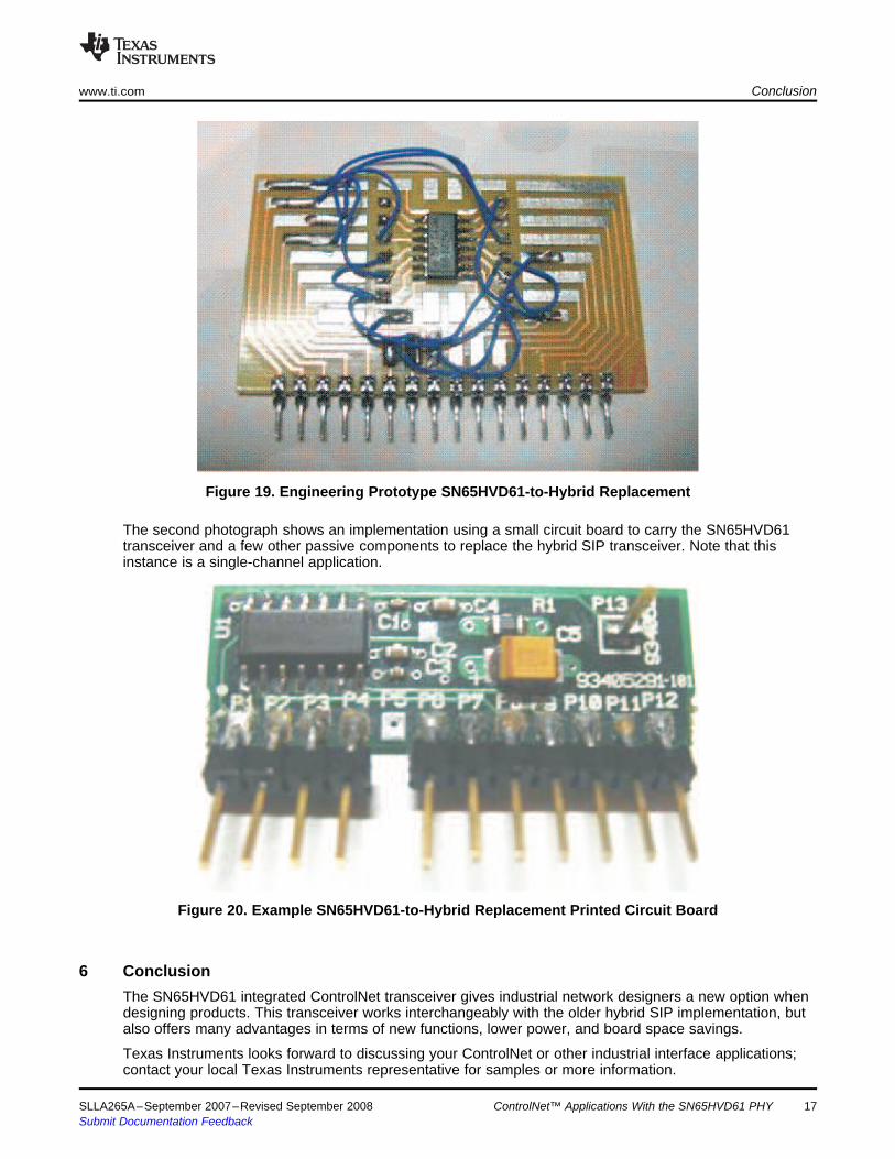
The two photographs below show two implementations of using the SN65HVD61 as a direct replacementfor the hybrid transceiver. In the first photo, an engineering version is shown. The surf board can bequickly wired as shown (refer to Table 2 for pin assignments). These prototype boards are available fromsources such as Capital Advanced Technologies (capitaladvanced.com). The specific board shown in thisfigure is Capital Advanced part number 9165.
16 ControlNet™ Applications With the SN65HVD61 PHY SLLA265A–September 2007–Revised September 2008Submit Documentation Feedback
6 Conclusion
www.ti.com Conclusion
Figure 19. Engineering Prototype SN65HVD61-to-Hybrid Replacement
The second photograph shows an implementation using a small circuit board to carry the SN65HVD61transceiver and a few other passive components to replace the hybrid SIP transceiver. Note that thisinstance is a single-channel application.
Figure 20. Example SN65HVD61-to-Hybrid Replacement Printed Circuit Board
The SN65HVD61 integrated ControlNet transceiver gives industrial network designers a new option whendesigning products. This transceiver works interchangeably with the older hybrid SIP implementation, butalso offers many advantages in terms of new functions, lower power, and board space savings.
Texas Instruments looks forward to discussing your ControlNet or other industrial interface applications;contact your local Texas Instruments representative for samples or more information.
SLLA265A–September 2007–Revised September 2008 ControlNet™ Applications With the SN65HVD61 PHY 17Submit Documentation Feedback

IMPORTANT NOTICETexas Instruments Incorporated and its subsidiaries (TI) reserve the right to make corrections, modifications, enhancements, improvements,and other changes to its products and services at any time and to discontinue any product or service without notice. Customers shouldobtain the latest relevant information before placing orders and should verify that such information is current and complete. All products aresold subject to TI’s terms and conditions of sale supplied at the time of order acknowledgment.TI warrants performance of its hardware products to the specifications applicable at the time of sale in accordance with TI’s standardwarranty. Testing and other quality control techniques are used to the extent TI deems necessary to support this warranty. Except wheremandated by government requirements, testing of all parameters of each product is not necessarily performed.TI assumes no liability for applications assistance or customer product design. Customers are responsible for their products andapplications using TI components. To minimize the risks associated with customer products and applications, customers should provideadequate design and operating safeguards.TI does not warrant or represent that any license, either express or implied, is granted under any TI patent right, copyright, mask work right,or other TI intellectual property right relating to any combination, machine, or process in which TI products or services are used. Informationpublished by TI regarding third-party products or services does not constitute a license from TI to use such products or services or awarranty or endorsement thereof. Use of such information may require a license from a third party under the patents or other intellectualproperty of the third party, or a license from TI under the patents or other intellectual property of TI.Reproduction of TI information in TI data books or data sheets is permissible only if reproduction is without alteration and is accompaniedby all associated warranties, conditions, limitations, and notices. Reproduction of this information with alteration is an unfair and deceptivebusiness practice. TI is not responsible or liable for such altered documentation. Information of third parties may be subject to additionalrestrictions.Resale of TI products or services with statements different from or beyond the parameters stated by TI for that product or service voids allexpress and any implied warranties for the associated TI product or service and is an unfair and deceptive business practice. TI is notresponsible or liable for any such statements.TI products are not authorized for use in safety-critical applications (such as life support) where a failure of the TI product would reasonablybe expected to cause severe personal injury or death, unless officers of the parties have executed an agreement specifically governingsuch use. Buyers represent that they have all necessary expertise in the safety and regulatory ramifications of their applications, andacknowledge and agree that they are solely responsible for all legal, regulatory and safety-related requirements concerning their productsand any use of TI products in such safety-critical applications, notwithstanding any applications-related information or support that may beprovided by TI. Further, Buyers must fully indemnify TI and its representatives against any damages arising out of the use of TI products insuch safety-critical applications.TI products are neither designed nor intended for use in military/aerospace applications or environments unless the TI products arespecifically designated by TI as military-grade or "enhanced plastic." Only products designated by TI as military-grade meet militaryspecifications. Buyers acknowledge and agree that any such use of TI products which TI has not designated as military-grade is solely atthe Buyer's risk, and that they are solely responsible for compliance with all legal and regulatory requirements in connection with such use.TI products are neither designed nor intended for use in automotive applications or environments unless the specific TI products aredesignated by TI as compliant with ISO/TS 16949 requirements. Buyers acknowledge and agree that, if they use any non-designatedproducts in automotive applications, TI will not be responsible for any failure to meet such requirements.Following are URLs where you can obtain information on other Texas Instruments products and application solutions:Products ApplicationsAmplifiers amplifier.ti.com Audio www.ti.com/audioData Converters dataconverter.ti.com Automotive www.ti.com/automotiveDSP dsp.ti.com Broadband www.ti.com/broadbandClocks and Timers www.ti.com/clocks Digital Control www.ti.com/digitalcontrolInterface interface.ti.com Medical www.ti.com/medicalLogic logic.ti.com Military www.ti.com/militaryPower Mgmt power.ti.com Optical Networking www.ti.com/opticalnetworkMicrocontrollers microcontroller.ti.com Security www.ti.com/securityRFID www.ti-rfid.com Telephony www.ti.com/telephonyRF/IF and ZigBee® Solutions www.ti.com/lprf Video & Imaging www.ti.com/video
Wireless www.ti.com/wireless
Mailing Address: Texas Instruments, Post Office Box 655303, Dallas, Texas 75265Copyright © 2008, Texas Instruments Incorporated