convolutional neural networks for image recognition … abstract—in this work, we devise and...
TRANSCRIPT

1
Abstract—In this work, we devise and optimize the schemes for
RRAM-based hardware implementation of convolutional neural
networks. The key achievements include: (1) A specific CNN
circuit and corresponding operation methods are presented. (2)
Quantification methods for utilizing binary RRAM or RRAM with
multilevel resistances as synapses are proposed, and simulations
show that our CNN system performs with 98% accuracy on the
MNIST dataset using multilevel RRAM and 97% accuracy using
binary RRAM as synapses. (3) The influence of factors such as the
number and the size of kernels as well as the device conductance
variation on final recognition accuracy is discussed. Three ways to
reduce hardware cost are analyzed. (4) We realize the function of
online learning using the developed CNN system with a binary
STDP protocol, and achieve up to 94% accuracy on the online
learning tasks.
Index Terms—Resistive random access memory (RRAM),
synapse, convolutional neural networks (CNN), online learning,
image recognition
I. INTRODUCTION
HE use of convolutional neural networks (CNN) has been
hugely successful in the field of image recognition. [1] – [5]
However, most software convolutional neural network
algorithms are achieved by CPUs and GPUs, which are built
under the traditional Von Neumann architecture. [6] Since the
deep convolutional neural networks always need a huge amount
of training data (the standard training dataset of ImageNet
ILSVRC contains 1260,000 RGB images with size 256*256,
and the validation dataset with 50000 images and the test
dataset with 100000 images [7]) and utilize weight parameters
up to 108 magnitude (VGG-Net utilizes 138M parameters [8]),
the whole process of taking data from memory and sending
them to CPUs and GPUs for computing as well as sending the
results back for storage would become rather time-consuming
and could also lead to a huge hardware cost. [9]
Many researches have been made to achieve brain-inspired
computing architecture beyond the Von Neumann architecture
which could realize the integration of storage and computing
and thus support the software algorithm with higher speed and
lower hardware cost. [10] - [19] There are generally two
Z. Dong, Z. Zhou, Z. Li, C. Liu, P. Huang, L. Liu, X. Liu, and J. Kang are
with the Institute of Microelectronics, Peking University, Beijing 100871, China (e-mail: [email protected])
schemes for hardware implementation of convolutional neural
networks, which could be divided by using whether CMOS
circuits or non-volatile memory such as phase change memory
(PCM), resistive change memory (RRAM), conductive bridge
type memory (CBRAM), etc. as synapses.
The RRAM-based implementation of CNN can reduce
energy consumption, compute with a higher speed and
physically realize parallelism while using neural circuits and
auxiliary circuits which are easy to achieve. [20] However, the
number of alternative weight values depends on the available
resistance states. Considering the difficulty in operating and
switching precisely among a large number of resistance states,
it is hard to realize the weight precision utilized in the software
algorithms (mostly float32 precision). Moreover, the online
adjustment of synaptic weights, which tends to be small in the
majority of algorithms, is also difficult for RRAM-based
implementation of convolutional neural networks due to the
variation around resistance states of RRAM devices. Though
many research efforts have been made [21] - [29], there’s still a
gap between the software algorithm and the hardware
implementation in terms of applying RRAM as synapses
efficiently while maintaining recognition accuracy.
In this work, we propose an optimized scheme for RRAM-
based CNN implementation. Section II introduces the CNN
architecture and corresponding circuits that we used in our
system. The characteristics which are required to utilize RRAM
as synapses are illustrated in Section III. In Section IV, the
influence of the alternative weight values, the number of
convolutional kernels, the threshold of weight quantification
scheme and the variation of device conductance on recognition
accuracy is studied in details, and three ways to lower the
RRAM amount utilized in the CNN system are discussed. We
achieve the function of online learning based on the developed
CNN system using a binary STDP protocol and present the
results in Section V.
II. CNN ARCHITECTURE AND CIRCUITS
As shown in Fig.1, the input images of handwritten digits
Convolutional Neural Networks for Image
Recognition and Online Learning Tasks Based
on RRAM Devices
Zhen Dong, Student Member, IEEE, Zheng Zhou, Zefan Li, Chen Liu, Peng Huang, Member, IEEE,
Lifeng Liu, Xiaoyan Liu, Jinfeng Kang*, Senior Member, IEEE
Institute of Microelectronics, Peking University, Beijing 100871, China *Email: [email protected]
T

2
MNIST with size 28*28 are firstly applied to the convolutional
layer. Then the results are pooled and activated to generate
output features. Finally, the output features are reshaped to
vectors and conveyed to a fully-connected layer to make the
final decision.
The definition and formula of convolutional operation is
illustrated in Fig.2, where W is the convolutional kernel and P
is one area in the input image which has the same size as W. X
is one pixel of the output feature map which is equal to the sum
of every product of corresponding pixels in P and W. Therefore,
one pixel in the convoluted output feature corresponds to one
district in the input image, and X can become the whole feature
map by moving the area P.
Inspired by biological neurons, the classic neural model used
in algorithms is shown in Fig.3, where W is the weight of
synapses and f is the activation function. Frequently used
activation functions are sigmoid, tanh, ReLU, or Leaky ReLU.
[30] We utilize ReLU in this work because it is easy for
hardware implementation, and it is linear when the input is
positive, which enables us to use RRAM conductance that are
proportional to rather than equal to software weights to
represent synaptic weights in our system.
Fig.4 shows the realization of the convolutional layer with
activation and pooling operations. Four rows of RRAM create
four output values corresponding to four adjacent districts in the
input image. Namely the blue RRAMs in the first row
correspond to one selected area, and the blue RRAMs in the
second row correspond to an adjacent area, and so on. The blank
points in the RRAM crossbar array represent RRAMs which are
not processed by a forming operation. Thus those RRAMs have
extremely high resistance and work as zero weights in the
system.
To represent negative weight values, two rows of RRAM are
used as one kernel, namely 𝐼𝑜𝑢𝑡 = 𝐼1 − 𝐼2 and thus 𝑊𝑒𝑓𝑓 =
𝑊1 −𝑊2 ( 𝑊𝑒𝑓𝑓 is the effective weight). Traditionally,
activation comes before the pooling operation. Changing the
sequence can make circuit implementation easier while having
little effect on the recognition accuracy. It should be noted that
another advantage of utilizing ReLU activation function is that
its linearity allows us to achieve 2*2 mean pooling operation by
simply combining four currents together without division
circuits. The integrated currents will then be activated and
converted to output voltages, which serve as the input signal of
the fully-connected layer.
Fig.1 The architecture of RRAM-based convolutional neural
network. The first layer is a convolutional layer and the last
layer is a fully-connected layer. Between them are pooling,
activation and reshaping operations.
Fig.4 Specific circuit of convolutional neural networks. Two
rows of RRAM work as one kernel and each eight output
currents are pooled and activated together to compute one value
in the output matrix, which will be conveyed to the fully-
connected layer.
Fig.2 Schematic of the convolution operation between an input
image and a learned kernel.
Fig.3 (a) Schematic of biological neuron and its components.
(b) The neural model used in neural network algorithms. (c)
Common types of activation functions.

3
III. DEVICE CHARACTERISTICS
Fig.5 shows the process flow for the fabrication of our
RRAM crossbar array. TiN and Pt are utilized as top electrode
and bottom electrode respectively, and AlOx/HfOy material is
used as the resistance change layer of RRAM.
Typical DC I-V characteristics of the AlOx/HfOy-based
RRAM are presented in Fig.6, where the black curve
corresponds to a set process and the red curve corresponds to a
reset process. The proportion between HRS and LRS, namely
the resistive window, is around 103 magnitude.
In order to use a large number of alternative weight values in
the quantification methods, conductance states are obtained by
adding small reset pulses as Fig.7(a) shows. The related change
of conductive filament in RRAM device is illustrated in
Fig.7(b). [31]
Considering the efficiency of training, a feasible operation
scheme among conductance states is proposed, as shown in
Fig.8. We measured two couples of conductance states. When
added a 1.2V 100ns pulse, the conductance state related to the
green curve is set to a high conductance, which corresponds to
the blue curve. And the state related to the blue curve can be
reset back by applying a -1.4V 100ns pulse. The same way goes
with the red conductance state and the black conductance state.
The conductance proportion between the green state and the
blue state is around 3 while that between the red and black states
are around 4. Taking the couple of green and blue states as an
example, because 𝑊𝑒𝑓𝑓 = 𝑊1 −𝑊2 , two conductance states
with a proportion of 1:3 can represent weights 0, ±1, ±2, ±3
(using the HRS as a zero weight). By the way, the reason of
utilizing the HRS rather than the conductance difference of two
equal LRS to represent 0 weight is that the latter would increase
the energy consumption since a low resistance state
corresponds to a large current under the same voltage. Because
2 LRS and 1 HRS are used for achieving 4 alternative absolute
weight values, we name the scheme a 3-state scheme.
In addition, the conductance variations of the states in Fig.8
are approximately 13.4%, 28.3%, 10.2% and 4.7%, corresponds
to the green, red, blue, black conductance state respectively.
Based on our test, the HRS variation is generally much larger
than the LRS variation, and this statement is still right when we
consider the variation of conductance states. Since the
resistance transition between the red and black states are larger
than that of the green and blue states, the variation of the red
curve tends to be large. However, because we utilize HRS as
low weight values in our CNN system where the high weight
values actually play a more important role, the problem of
relatively large HRS variation could be naturally settled in our
system.
IV. RESULTS AND DISCUSSIONS
Fig.9 shows the relationship between accuracy and the
number of alternative weight values (No. of |w|) realized by
RRAM with multilevel resistances. It could be pointed out that
if the alternative number of weights is larger than 4, decreasing
the precision of software weight value won’t cause considerable
reduction of the recognition accuracy. Hence, 4 alternative
-2 -1 0 1 2
10-8
10-7
10-6
10-5
10-4
10-3
Cu
rre
nt(
A)
Voltage(V)
Fig.5 Process flow for the AlOx/HfOy-based RRAM crossbar
array fabrication. Corresponding schematic diagram of each
step is shown.
0 200 400 600 800 1000
0.0
0.5
1.0
1.5
2.0
2.5
Co
nd
uc
tan
ce
(mS
)
Number of Pulse
Fig.6 Measured typical DC I-V characteristics of RRAM device
in a crossbar array.
0.4 0.8 1.2 1.6 2.0
0
20
40
60
80
100
-1.4V 100ns
1.2V 100ns
-1.4V 100ns
Cu
mu
lati
ve
Pro
ba
bil
ity
(%
)
Conductance (mS)
1.3V 100ns
Fig.7(a) Conductance states obtained by adding increasing
number of small continuous AC reset pulses. (b) The shape
change of conductive filament corresponding to each stage in
the conductance transition curve.
Fig.8 Conductance states (to be used as quantified weights in
the networks) and corresponding writing methods for RRAM
devices.

4
value scheme and binary scheme are more efficient. To obtain
recognition accuracy higher than 95%, the binary RRAM
scheme needs at least 10 kernels, while the RRAM with 3-state
scheme (namely the 4 alternative scheme) needs only 5 kernels.
Besides, according to the figure, when the number of kernels is
larger than 10, increasing kernel number won’t contribute to the
rise of recognition accuracy, thus 10 kernels scheme is
considered efficient.
Fig.10 is the frequency histogram of software weight values.
When we utilize RRAM as synapses, a quantification scheme
is needed to convert software values to RRAM alternative
weight values. A good quantification scheme is supposed to
maintain the standard deviation of the quantified weights close
to that of the original weights. An extreme example of a bad
quantification method is to set the threshold very large, then all
the weights become zero and the network will become useless.
Moreover, the total number of weights in W2 is much larger
than the number of weights in W1, thus according to the
statistical laws, the distribution curve of W2 is more smooth
than that of W1.
The quantification threshold is crucial for the RRAM-based
system especially when we utilize the binary scheme. It decides
a software weight value corresponds to whether -1, 0 or 1 and
can affect the recognition accuracy significantly. Fig.10 (a)
shows the influence of W1 threshold on recognition accuracy
with W2 threshold fixed (W1 are weights in convolutional
kernels and W2 are weights in the fully-connected layer). It
could be seen from the figure that when W1 threshold is
between 12 to 23, the recognition accuracy gets its maximum
97%. Fig.11 (b) shows the relationship between W2 threshold
and the recognition accuracy with W1 threshold fixed, and 1 to
11 are acceptable range of W2 threshold.
Fig.12 illustrates the system’s tolerance to the variation of
device conductance. When variation increases, the average
accuracy begins to fall and the fluctuation of recognition
accuracy gets larger. Hence, keeping the variation, especially
the variation of high conductance, lower than 50% is necessary.
Fortunately, according to the measured variation of high
conductance states of our AlOx/HfOy-based RRAM in Fig.8,
the 50% requirement could be easily fulfilled. Besides, the
accuracy of the binary scheme is always lower than that of the
3-state scheme, and the fluctuation of the former tends to be
larger than the latter in the same situation.
The discussions above mainly focus on improving
recognition performance rather than reducing the hardware cost.
When the total amount of RRAMs is considered a crucial
criterion of the CNN system, there are generally three ways for
saving RRAMs. Fig.13 shows the relationship between the
2 4 6 8 1080
85
90
95
100
Accu
racy(%
)
No. of alternative weight values
25
20
15
10
5
3
No. of kernels
Fig.9 Recognition accuracy as a function of the number of
kernels and alternative weight values.
5 10 15 20 25 30
75
80
85
90
95
100
Ac
cu
rac
y(%
)
Threshold of W1 weights
2
5
8
11
14
W2 threshold
0 20 40 60 80 100
40
60
80
100
2-state scheme
binary schemeAcc
ura
cy(%
)
Variation(%)
Fig.12 The influence of device conductance variation on
recognition accuracy.
Fig.11 (a) The influence of W1 weight threshold on recognition
accuracy (keep W2 weight threshold constant) (b) The
influence of W2 weight threshold on recognition accuracy
(keep W1 weight threshold constant).
-80 -60 -40 -20 0 20 40 60 800
20
40
60
80
Nu
mb
er
W1 weights values-40 -20 0 20 40
0.0
500.0
1.0k
1.5k
2.0k
Nu
mb
er
W2 weights values
Fig.10 The frequency histogram of the weight value
distribution in (a) convolutional kernels and (b) fully-
connected layer.
0 2 4 6 8 10 12 14 16 1875
80
85
90
95
100
Ac
cu
rac
y(%
)
Threshold of W2 weights
11
14
17
20
23
W1 threshold
5
number of RRAMs and the size of convolutional kernels. When
the kernel size is small, the cost of RRAMs in the fully-
connected layer is much higher than that in the convolutional
layer, and the total number tends to be large. However, utilizing
very large kernels could cause a huge cost of RRAMs in the
convolutional layer and also reduce the recognition accuracy
due to the incapacity of the fully-connected layer. Thus,
choosing a medium kernel size can make the CNN system more
cost-effective.
The second way of lowering hardware cost is to trim the
original input images, which could make the output features of
the convolutional layer become smaller and thus effectively
reduce the number of parameters in the fully-connected layer.
As Fig.14 shows, since the RRAM amount used in fully-
connected layer is rather small when large kernels are utilized,
the effect of trimming is not as good as other cases. In addition,
trimming the original inputs from 28×28 to very small sizes
would cause the loss of original information and influence the
recognition performance, thus the sizes smaller than 18×18 are
not shown in Fig.14.
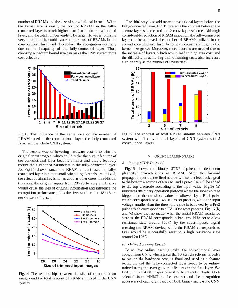
The third way is to add more convolutional layers before the
fully-connected layer. Fig.15 presents the contrast between the
1-conv-layer scheme and the 2-conv-layer scheme. Although
considerable reduction of RRAM amount in the fully-connected
layer can be achieved, the number of RRAMs utilized in the
second convolutional layer becomes increasingly huge as the
kernel size grows. Moreover, more neurons are needed due to
the increase of layers, which would lead to high area cost, and
the difficulty of achieving online learning tasks also increases
significantly as the number of layers rises.
V. ONLINE LEARNING TASKS
A. Binary STDP Protocol
Fig.16 shows the binary STDP (spike-time dependent
plasticity) characteristics of RRAM. After the forward
propagation period, the fired neuron will send a feedback signal
to the bottom electrode of RRAM, and a pre-pulse will be added
to the top electrode according to the input value. Fig.16 (a)
illustrates the binary operation protocol where the input voltage
bigger than the threshold value is followed by a Pre1 pulse
which corresponds to a 1.4V 100ns set process, while the input
voltage smaller than the threshold value is followed by a Pre2
pulse which corresponds to a 2V 100ns reset process. Fig.16 (b)
and (c) show that no matter what the initial RRAM resistance
state is, the RRAM corresponds to Pre1 would be set to a low
resistance state around 500Ω by the superimposed signal
crossing the RRAM device, while the RRAM corresponds to
Pre2 would be successfully reset to a high resistance state
around 2×10⁵Ω.
B. Online Learning Results
To achieve online learning tasks, the convolutional layer
copied from CNN, which takes the 10 kernels scheme in order
to reduce the hardware cost, is fixed and used as a feature
extractor, and the fully-connected layer needs to be online-
trained using the average output features in the first layer. We
firstly utilize 7000 images consist of handwritten digits 0 to 6
selected from MNIST as the test set and the recognition
accuracies of each digit based on both binary and 3-state CNN
1 3 5 7 9 11 13 15 17 19 21 23 25 270
5
10
15
20
25
30
35
40
To
tal n
um
ber
of
RR
AM
s (
k)
Size of kernels
Convolutional Layer
Fully-connected Layer
Total Number
Fig.13 The influence of the kernel size on the number of
RRAMs used in the convolutional layer, the fully-connected
layer and the whole CNN system.
28 26 24 22 20 18
5
10
15
20
25
30
To
tal n
um
ber
of
RR
AM
s (
k)
Size of trimmed input images
5×5 kernels
9×9 kernels
13×13 kernels
17×17 kernels
Fig.14 The relationship between the size of trimmed input
images and the total amount of RRAMs utilized in the CNN
system.
3 5 7 90
5
10
15
20
25
30
35
To
tal
nu
me
r o
f R
RA
Ms
(k
)Size of kernels
Fully-connected Layer
Convolutional Layer
Fig.15 The contrast of total RRAM amount between CNN
system with 1 convolutional layer and CNN system with 2
convolutional layers.

6
kernel weights are shown in Fig.17. The average performance
using binary convolutional weights is 93.63%, which is a little
lower than the recognition accuracy using 3-state weight
scheme (94.04%).
We also present the results on the whole 10000 handwritten
images of the MNIST test set where a 91.80% average
recognition accuracy is obtained using the 3-state scheme and
an 91.18% recognition accuracy is obtained using the binary
scheme.
In addition, the recognition accuracy of digits 7 and 9 in this
trial is worse than the others, however, it won’t be always that
way. If we train another network from scratch, then digits 4 and
8 may turn out to get worse recognition accuracy. Nevertheless,
it should be noted that the average recognition accuracy of 10
digits is always worse than that of 7 digits, which actually
shows the difficulty difference between those two tasks.
VI. CONCLUSION
Convolutional neural network architecture and
corresponding circuits are optimized in this work. Multilevel
resistance states of RRAM are measured and utilized in RRAM-
based implementation of CNN. Different factors that affect
recognition accuracy are analyzed in detail. Three ways to
reduce the hardware cost are proposed. Finally, the online
learning tasks are accomplished based on the developed CNN
system.
ACKNOWLEDGMENT
This work was supported in part by the NSFC (61334007,
61421005), National Innovation Training Program, and Beijing
Municipal Science and Technology Plan Projects.
REFERENCES
[1] K Krizhevsky A, Sutskever I, Hinton G E. Imagenet classification with
deep convolutional neural networks[C]//Advances in neural information processing systems. 2012: 1097-1105.
[2] LeCun Y, Kavukcuoglu K, Farabet C. Convolutional networks and
applications in vision[C]//Circuits and Systems (ISCAS), Proceedings of
2010 IEEE International Symposium on. IEEE, 2010: 253-256.
[3] LeCun Y, Bengio Y, Hinton G. Deep learning[J]. Nature, 2015,
521(7553): 436-444. [4] Silver D, Huang A, Maddison C J, Guez A, Sifre L, Van Den Driessche
G, ... and Dieleman S. Mastering the game of Go with deep neural
networks and tree search[J]. Nature, 2016, 529(7587): 484-489. [5] He K, Zhang X, Ren S, Sun J. Deep residual learning for image
recognition[C]//Proceedings of the IEEE conference on computer vision
and pattern recognition. 2016: 770-778. [6] Akopyan F, Sawada J, Cassidy A, Alvarez-Icaza R, Arthur J, Merolla P, ...
and Taba B. Truenorth: Design and tool flow of a 65 mw 1 million neuron
programmable neurosynaptic chip. IEEE Transactions on Computer-Aided Design of Integrated Circuits and Systems, 2015, 34(10), 1537-
1557.
[7] Russakovsky O, Deng J, Su H, Krause J, Satheesh S, Ma S, Huang Z, Karpathy A, Khosla A, Bernstein M, Berg A C, and Fei-Fei L. ImageNet
large scale visual recognition challenge. CoRR, abs/1409.0575, 2014.
Fig.16 (a) Waveform used in binary STDP learning system. (b)
Measured LTP characteristics of RRAM at different initial
resistance. (c) Measured LTD characteristics of RRAM at
different initial resistance. Δt is the time difference between Pre
and Post signal.
-1000 0 1000 2000 3000
103
104
105
Re
sis
tan
ce
(Oh
m)
Delta t (ns)
-1000 0 1000 2000 3000
103
104
105
Re
sis
tan
ce
(Oh
m)
Delta t (ns)
0 1 2 3 4 5 6
85
90
95
100
Ac
cu
rac
y(%
)
Digit for Recognition
2-state scheme
Binary scheme
Average 94.04%
Average 93.63%
Fig.17 Recognition results of 0~6 digits respectively, based on
both binary weight CNN and 3-state weight CNN. The average
accuracy of each scheme is illustrated with dotted line.
0 1 2 3 4 5 6 7 8 9
85
90
95
100
Average 91.18%
Average 91.80%
Ac
cu
rac
y(%
)
Digit for Recognition
2-state scheme
Binary scheme
Fig.18 Recognition results of 0~9 digits respectively, based on
both binary weight CNN and 3-state weight CNN. The average
accuracy of each scheme is illustrated with dotted line.

7
[8] Simonyan K, Zisserman A. Very deep convolutional networks for large-
scale image recognition[J]. preprint arXiv:1409.1556, 2014. [9] Von Neumann J. The computer and the brain[M]. Yale University Press,
2012.
[10] Kinget P, Steyaert M S J. A programmable analog cellular neural network CMOS chip for high speed image processing[J]. IEEE Journal of Solid-
State Circuits, 1995, 30(3): 235-243.
[11] Indiveri G, Chicca E, Douglas R. A VLSI array of low-power spiking neurons and bistable synapses with spike-timing dependent plasticity[J].
IEEE transactions on neural networks, 2006, 17(1): 211-221.
[12] Milo V, Pedretti G, Carboni R, Calderoni A, Ramaswamy N, Ambrogio S, and Ielmini D. Demonstration of hybrid CMOS/RRAM neural
networks with spike time/rate-dependent plasticity. 2016 IEEE
International Electron Devices Meeting (IEDM), 2016: p. 16.8.1-4. [13] Kim K H, Gaba S, Wheeler D, Cruz-Albrecht J M, Hussain T, Srinivasa
N and Lu W. A functional hybrid memristor crossbar-array/CMOS
system for data storage and neuromorphic applications[J]. Nano letters, 2011, 12(1): 389-395.
[14] Gao B, Bi Y, Chen H Y, Liu R, Huang P, Chen B, ... and Kang J. Ultra-
low-energy three-dimensional oxide-based electronic synapses for implementation of robust high-accuracy neuromorphic computation
systems[J]. ACS nano, 2014, 8(7): 6998-7004.
[15] Eryilmaz S B, Kuzum D, Yu S, H.-S. Philip Wong. Device and system level design considerations for analog-non-volatile-memory based
neuromorphic architectures[C]//Electron Devices Meeting (IEDM), 2015
IEEE International. IEEE, 2015: 4.1. 1-4.1. 4. [16] Yu S, Gao B, Fang Z, Yu H, Kang J, and H.-S. Philip Wong. A low energy
oxide‐based electronic synaptic device for neuromorphic visual systems with tolerance to device variation[J]. Advanced Materials, 2013, 25(12):
1774-1779.
[17] Burr G W, Shelby R M, Sidler S, Di Nolfo C, Jang J, Boybat I, ... and Kurdi B N. Experimental demonstration and tolerancing of a large-scale
neural network (165 000 synapses) using phase-change memory as the
synaptic weight element[J]. IEEE Transactions on Electron Devices, 2015, 62(11): 3498-3507.
[18] Suri M, Querlioz D, Bichler O, Palma O, Vianello G, Vuillaume E, ... and
DeSalvo B. Bio-inspired stochastic computing using binary CBRAM synapses[J]. IEEE Transactions on Electron Devices, 2013, 60(7): 2402-
2409.
[19] B. Gao, H. Wu, J. Kang, H. Yu, and H. Qian. Oxide-based analog synapse: Physical modeling, experimental characterization, and
optimization[C]//Electron Devices Meeting (IEDM), 2016 IEEE
International. IEEE, 2016: 7.3. 1-7.3. 4. [20] Wang I T, Lin Y C, Wang Y F, Hsu C W, and Hou T H. 3D synaptic
architecture with ultralow sub-10 fJ energy per spike for neuromorphic
computation[C]//Electron Devices Meeting (IEDM), 2014 IEEE International. IEEE, 2014: 28.5. 1-28.5. 4.
[21] Ambrogio S, Balatti S, Milo V, Carboni R, Wang Z Q, Calderoni A, ...
and Ielmini D. Neuromorphic learning and recognition with one-transistor-one-resistor synapses and bistable metal oxide RRAM[J]. IEEE
Transactions on Electron Devices, 2016, 63(4): 1508-1515.
[22] Alibart F, Zamanidoost E, Strukov D B. Pattern classification by memristive crossbar circuits using ex situ and in situ training[J]. Nature
communications, 2013, 4: 2072.
[23] Park S, Kim H, Choo M, Noh J, Sheri A, Jung S, ... and Shin J. RRAM-based synapse for neuromorphic system with pattern recognition
function[C]//Electron Devices Meeting (IEDM), 2012 IEEE International.
IEEE, 2012: 10.2. 1-10.2. 4. [24] Garbin D, Vianello E, Bichler O, Rafhay Q, Gamrat C, Ghibaudo G, ...
and Perniola L. HfO2-based OxRAM devices as synapses for
convolutional neural networks[J]. IEEE Transactions on Electron Devices, 2015, 62(8): 2494-2501.
[25] J. Woo, K. Moon, J. Song, M. Kwak, J. Park, and H. Hwang. Optimized
programming scheme enabling linear potentiation in filamentary HfO2 RRAM synapse for neuromorphic systems[J]. IEEE Transactions on
Electron Devices, 2016, 63(12): 5064-5067.
[26] Zhou Z, Liu C, Shen W, Dong Z, Chen Z, Huang P, ... and Kang J. The Characteristics of Binary Spike-Time-Dependent Plasticity in HfO2-
Based RRAM and Applications for Pattern Recognition[J]. Nanoscale
Research Letters, 2017, 12(1): 244. [27] Yu S, Li Z, Chen P Y, Wu H, Gao B, Wang D, ... and Qian H. Binary
neural network with 16 Mb RRAM macro chip for classification and
online training[C]//Electron Devices Meeting (IEDM), 2016 IEEE International. IEEE, 2016: 16.2. 1-16.2. 4.
[28] Prezioso M, Merrikh-Bayat F, Hoskins B D, Adam G C, Likharev K K,
and Strukov D B. Training and operation of an integrated neuromorphic network based on metal-oxide memristors[J]. Nature, 2015, 521(7550):
61-64.
[29] Hu S G, Liu Y, Liu Z, Chen T P, Wang J J, Yu Q, ... and Hosaka S. Associative memory realized by a reconfigurable memristive Hopfield
neural network[J]. Nature communications, 2015, 6.
[30] Fei-fei Li, Andrej Karpathy, Justin Johnson. CS231n Stanford. (2016). Cs231n: Convolutional neural networks for visual recognition.
[31] Chen Z, Gao B, Zhou Z, Huang P, Li H, Ma W, ... and Chen H
Y. Optimized learning scheme for grayscale image recognition in a RRAM based analog neuromorphic system[C]//Electron Devices Meeting
(IEDM), 2015 IEEE International. IEEE, 2015: 17.7. 1-17.7. 4.
Zhen Dong (S’16) is pursuing the B.S.
degree in the Institute of Microelectronics,
Peking University, Beijing, China. He has
been a research assistant in the Institute of
Microelectronics since 2015 and currently
works in Stanford University as an
undergraduate visiting researcher.
His research interests include hardware
neuromorphic systems, deep learning
accelerators and non-volatile memories.
Zheng Zhou received the B.E. degree
from the Nanjing University of
Aeronautics and Astronautics, Nanjing,
China, in 2013. He is currently pursuing
the Ph.D. degree with the Institute of
Microelectronics, Peking University,
Beijing, China.
His current research interests include
RRAM and its application in
neuromorphic computing.
Zefan Li is currently working toward the
B. S. degree with the Institute of
Electronics, Peking University, Beijing,
China. His current research interests
include neuromorphic machine learning
and non- Von Neumann computing
architecture based on resistance random
access memory.
Chen Liu received the B.S. degree from
Peking University, Beijing, China, in
2014. He is currently working toward the
Ph.D. degree in the Institute of
Microelectronics, Peking University,
Beijing, China.

8
Lifeng Liu received the Ph.D. degree in
materials physics and chemistry from the
Institute of Semiconductors, Chinese
Academy of Sciences, Beijing, China, in
2005. He is currently an Associate
Professor with the Institute of
Microelectronics, Peking University,
Beijing.
Peng Huang (M’16) received the B.S.
degree from Xidian University, Xi’an,
China, in 2010 and the Ph.D. degree in
microelectronics from Peking University,
Beijing, China in 2015. He is currently a
Postdoctoral Associate in the Institute of
Microelectronics, Peking University. His
research interest is RRAM and its
application in computing.
Xiaoyan Liu received the B.S., M.S., and
Ph.D. degrees in microelectronics from
Peking University, Beijing, China, in
1988, 1991, and 2001, respectively. She is
currently a Professor with Institute of
Microelectronics, Peking University.
Jinfeng Kang received the Ph.D. degree
in solid state electronics from Peking
University, Beijing, China, in 1995. He is
currently a Professor in the Institute of
Microelectronics, Peking University.