coplanar-gate transparent graphene transistors and...
TRANSCRIPT

KIM ET AL. VOL. XXX ’ NO. XX ’ 000–000 ’ XXXX
www.acsnano.org
A
CXXXX American Chemical Society
Coplanar-Gate Transparent GrapheneTransistors and Inverters on PlasticBeom Joon Kim,†,# Seoung-Ki Lee,‡,# Moon Sung Kang,§ Jong-Hyun Ahn,‡,* and Jeong Ho Cho†,*
†School of Chemical Engineering and ‡School of Advanced Materials Science and Engineering, SKKU Advanced Institute of Nanotechnology (SAINT) and Center forHuman Interface Nano Technology (HINT), Sungkyunkwan University, Suwon 440-746, Korea, and §Department of Chemical Engineering, Soongsil University,Seoul 156-743, Korea. #B. J. Kim and S.-K. Lee contributed equally to this work.
Graphene has attracted significantattention due to its optical transpar-ency, mechanical flexibility, and
high carrier mobility.1�6 To exploit theseproperties of graphene in large-area flexibleelectronics, a variety of printing methods ofgraphene and other device componentshave been developed. For example, assem-bling graphene-based thin-film transistors(TFTs) can be achieved using combinationsof transfer-printing techniques applied tographene films grown by chemical vapor de-position (CVD) or graphene oxide dispersion-based solution processes with various print-ingmethods of gate dielectric and electrode,which have been investigated extensively inthe field of organic electronics.7�9
Fromapractical perspective, the progressin printed graphene electronics could befurther accelerated using a simpler TFT con-figuration that would require fewer printingsteps.10,11 Graphene is, in fact, an excellentmaterial for use in TFTs with simplifiedconfigurations. As a single material, gra-phene features both semiconducting andmetallic behavior and thus can function asa semiconductor channel as well as anelectrode.12�15 Therefore, the active chan-nels and source/drain electrodes can beformed using a monolithic graphene layer
via a single printing process.16 Also, the use
of electrical double layer capacitors as gate
dielectrics can alleviate constraints on the
positions of the gate electrodes.17,18 Conse-
quently, the development of graphene-
based TFTs with unconventional and simple
device configurations is highly promising.To this end, we demonstrate the prepara-
tion of transparent flexible graphene transis-tors with a coplanar gate configuration basedonlyon twomaterials, grapheneandan iongelgate dielectric. Moreover, flexible complemen-tary graphene inverters prepared on a plasticsubstrate are presented for the first time byconnecting two coplanar-gate graphene
transistors. A single graphene transistorconsists of a main graphene strip, a patchof graphene (with split arms) positionedaway from the main strip, and an ion gelgate dielectric bridging the two compo-nents. The main strip of graphene functionsas an active semiconducting channel andthe source/drain electrodes, depending onits contact with the ion gel. The split arms,which are patterned to be coplanar with themain graphene strip, serve as the gateelectrode. This unconventional device ge-ometry with a coplanar-gate configurationdramatically simplifies the device fabrica-tion such that only two printing steps wererequired to fabricate transistors and inver-ters. The resulting coplanar gate graphenetransistors exhibit excellent device perfor-mances including low-voltage operationwith ahigh transistor-on-current andmobility,
* Address correspondence [email protected],[email protected].
Received for review May 9, 2012and accepted August 27, 2012.
Published online10.1021/nn3020486
ABSTRACT
Transparent flexible graphene transistors and inverters in a coplanar-gate configuration were
presented for the first time using only two materials: graphene and an ion gel gate dielectric.
The novel device configuration simplifies device fabrication such that only two printing steps
were required to fabricate transistors and inverters. The devices exhibited excellent device
performances including low-voltage operation with a high transistor-on-current and mobility,
excellent mechanical flexibility, environmental stability, and a reasonable inverting behavior
upon connecting the two transistors.
KEYWORDS: graphene transistor . coplanar-gate configuration . transparentelectronics . flexible electronics
ARTIC
LE
KIM ET AL. VOL. XXX ’ NO. XX ’ 000–000 ’ XXXX
www.acsnano.org
B
excellent mechanical flexibility, environmental stabil-ity, and a reasonable inverting behavior upon connect-ing the two transistors. Accordingly, the coplanar-gategraphene transistors provide a novel and simple routeto achieving low-cost printed flexible graphene elec-tronics with a high device performance.
RESULTS AND DISCUSSION
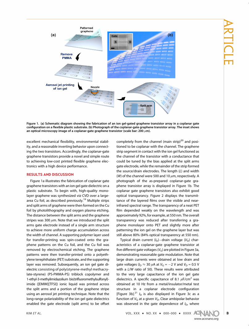
Figure 1a illustrates the fabrication of coplanar gategraphene transistorswith an ion gel gate dielectric on aplastic substrate. To begin with, high-quality mono-layer graphene was synthesized via CVD over a large-area Cu foil, as described previously.19 Multiple stripsand split arms of graphenewere then formedon the Cufoil by photolithography and oxygen plasma etching.The distance between the split arms and the graphenestripes was 300 μm. Note that we introduced the splitarms gate electrode instead of a single arm structureto achieve more uniform charge accumulation acrossthe width of channel. A supporting polymer layer usedfor transfer-printing was spin-coated onto the gra-phene patterns on the Cu foil, and the Cu foil wasremoved by electrochemical etching. The graphenepatterns were then transfer-printed onto a polyeth-ylene terephthalate (PET) substrate, and the supportinglayer was removed. Subsequently, an ion gel gate di-electric consisting of poly(styrene-methyl methacry-late-styrene) (PS-PMMA-PS) triblock copolymer and1-ethyl-3-methylimidazolium bis(trifluoromethylsulfonyl)-imide ([EMIM][TFSI]) ionic liquid was printed acrossthe split arms and a portion of the graphene stripeusing an aerosol jet printing technique. Note that thelong-range polarizability of the ion gel gate dielectricsenabled the gate electrode (split arms) to be offset
completely from the channel (main strip)20 and posi-tioned to be coplanar with the channel. The graphenestrip segment in contact with the ion gel functioned asthe channel of the transistor with a conductance thatcould be tuned by the bias applied at the split armsgate electrode, while the remainder of the strip formedthe source/drain electrodes. The length (L) and width(W) of the channel were 500 and 10 μm, respectively. Aphotograph of the as-prepared coplanar-gate gra-phene transistor array is displayed in Figure 1b. Thecoplanar gate graphene transistors also exhibit goodoptical transparancy. Figure 2 displays the transmit-tance of the layered films over the visible and near-infrared spectral range. The transparency of a neat PETfilm depended weakly on the wavelength and wasapproximately 92%, for example, at 550 nm. The overalltransparency was reduced after transferring a gra-phene monolayer onto PET and slightly more afterpatterning the ion gel on the graphene layer but wasstill above 80% (84% optical transparency at 550 nm).Typical drain current (ID)�drain voltage (VD) char-
acteristics of a coplanar-gate graphene transistor atfive different gate voltages (VG) are plotted in Figure 3a,demonstrating reasonable gate modulation. Note thatlarge drain currents were obtained at low drain andgate voltages (ID ≈ 30 μA at VG = �2 V and VD = 0.5 Vwith a L/W ratio of 50). These results were attributedto the very large capacitance of the ion gel gatedielectrics. A specific capacitance of 8.1 μF/cm2 wasobtained at 10 Hz from a metal/insulator/metal teststructure in a coplanar electrode configuration[Figure 3b].21 ID is also displayed in Figure 3c as afunction of VG at a given VD. Clear ambipolar behaviorwas observed in the gate dependence of ID, where
Figure 1. (a) Schematic diagram showing the fabrication of an ion gel-gated graphene transistor array in a coplanar gateconfiguration on a flexible plastic substrate. (b) Photograph of the coplanar-gate graphene transistor array. The inset showsan optical microscopy image of a coplanar-gate graphene transistor (scale bar: 200 μm).
ARTIC
LE

KIM ET AL. VOL. XXX ’ NO. XX ’ 000–000 ’ XXXX
www.acsnano.org
C
positive and negative VG regions represent electronand hole transport, respectively. Devices show the lowoperation voltages (<2 V) and the charge neutralitypoint (Dirac point) around 0 V. The operating speed ofthese devices, which is unavoidably associated withthe relatively slow motion of ions under gate field, isunder investigation.Estimating the mobility (μ) of the devices required a
more rigorous calculation to treat the monolithic
nature of the graphene devices. It is worth emphasiz-ing that the resistivity of the source and drain electro-des (the portion of the graphene strip not coveredwiththe ion gel) exceeds that of the channel (the portion ofthe graphene covered with the ion gel) when thedevice is turned on. These properties differ from thoseof conventional transistors in which the resistivity of anelectrode is, in general, much lower than that of achannel. As a result, accurate estimates of the channelresistance (Rchannel) should consider subtracting theelectrode resistance (Relectrode) from the total resis-tance (Rtotal) obtained directly from the raw I�V char-acteristics; Rchannel = Rtotal� Relectrode; Relectrode could bemeasured from a separate metal�graphene�metaltest structure constructed with the dimensions usedfor the graphene transistors, as shown in SupportingInformation, Figure S1. Accordingly, the channel con-ductivity (σchannel), obtained from Rchannel, can be dis-played as a function of the carrier density (n) at a givenVG, as shown in the inset of Figure 3c, using the channeldimensions and the following relation,22,23
jVG � VG,minj ¼ hνFffiffiffiffiffiffi
πnpe
þ ne
CEDLFigure 2. Transmittance of a PET substrate (black) withgraphene (red) and an ion gel layer (blue).
Figure 3. (a) Output characteristics (ID vs VD) of a coplanar-gate graphene transistor at five different VG values. (b) Frequencydependence of the specific capacitance of the ion-gel capacitor in graphene/ion�gel/graphene coplanar configuration. (c)Transfer characteristics (ID vsVG) of a coplanar-gate graphene transistor atVD=�0.1 V and the correspondingσchannel vs nplot(inset). (d) Distribution of the hole and electron mobilities from 50 coplanar-gate graphene transistors.
ARTIC
LE

KIM ET AL. VOL. XXX ’ NO. XX ’ 000–000 ’ XXXX
www.acsnano.org
D
where h is the reduced Planck's constant, νF is theFermi velocity (1.1 � 106 m/s), and CEDL is the electricdouble layer capacitance.24 Finally, the carrier mobilityis calculated according to μ = (dσchannel/dn)/e.Figure 3d displays the distributions of the hole andelectron mobilities of 50 devices that are randomlyselected among coplanar-gate graphene transistorsfabricated from different batches. A Gaussian fit indi-cates that the hole and electron mobilities werecentered on 892 ( 196 and 628 ( 146 cm2/(V 3 s),respectively. Moreover, the overall device yield isgreater than 95%; this is typical for many batches wehave examined. Note that these estimated values(excluding the influence of electrode resistance) de-termine the upper bound of the nominal mobilityvalues (including the influence of electrode resistancewhich may be practical for integrated circuit design).
The mechanical flexibility, robustness, and air sta-bility of the coplanar-gate graphene transistors wereinvestigated. Figure 4a shows the changes in theeffective hole and electron mobilities, measured inforward and backward bending tests and normalizedby the corresponding mobilities from the unbent state(μ/μo). Negative and positive strains corresponded totension and compression, respectively. Strains within(2.8% yielded only a 20% change in the hole andelectron mobilities. Fatigue tests were also performedon the graphene transistors. The inset of Figure 4ashows μ/μo after five thousand cycles of bending,which introduced tension strains between 0% and2%. The values of μ/μo changed relative to the initialvalues by only 20% after 5000 cycles. Finally, the devicestability under ambient conditions was tested. Asshown in Figure 4b, almost no appreciable degrada-tion in the device performance was observed, evenafter storing the devices under ambient conditionsfor more than one month. Overall, the bending tests,fatigue tests, and air stability tests demonstrated thestable and reliable operation of the flexible graphenetransistors.Finally, complementary inverters were prepared by
connecting two coplanar-gate graphene transistors ona plastic substrate; one of the transistors was con-nected to the supply voltage (VDD), the other wasconnected to the ground, and the two transistorsshared an input gate terminal and an output terminal,as shown in Figure 5a. The circuit diagram of aninverter is displayed in Figure 5b. It should be notedthat these devices were fabricated in two simple steps,including transfer printing of graphene and aerosolprinting of the ion gel. Details of the inverter operationbased on two identical ambipolar transistors, unlikethose of complementary inverters based on separaten- and p-channel transistors, are thoroughly describedin refs 25�27. Briefly, the effective channel potentialapplied to the two identical transistors varies respec-tively due to the drain potential superposition effectupon sweeping an input signal (VIN) under a constantVDD.
25�27 As a conseqence, their channel resistances
Figure 4. (a) The normalized hole/electron mobilities (μ/μo)as a function of strain induced by bending. The inset showsthe changes in μ/μo after multiple bending cycles at atension strain up to 2%. (b) Ambient air stability of gra-phene transistors. The insets show changes in the Diracpoint during the stability test.
Figure 5. (a) Schematic diagram of a complementary inverter based on two coplanar-gate graphene transistors. (b) Circuitdiagram of the inverter. (c) Transfer characteristics (ID vs VG) of a coplanar-gate graphene transistor at different VDS (from 0.1to 1 V), demonstrating that the channel resistance at a given gate field can vary if the effective channel potential (drain field)varies. The inset shows Vdirac vs VD plot. (d) Input�output voltage characteristic and corresponding gain of a complementaryinverter based on coplanar-gate graphene transistors.
ARTIC
LE

KIM ET AL. VOL. XXX ’ NO. XX ’ 000–000 ’ XXXX
www.acsnano.org
E
(R1 and R2) [Figure 5c] and the resulting output signal(VOUT), which follows VOUT = VDD[(R2/(R1 þ R2)],change accordingly to yield an inverted signal be-tween the input and the output. As an example,Figure 5d shows a typical VOUT �VIN relation of aninverter based on the coplanr-gate transistors at VDDof 1.5 V. Differing from a typical CMOS inverter, theoutput voltage did not saturate to zero or VDD dueto the zero band gap of graphene.28,29 VOUT �VINrelations at different values of VDD are displayed inSupporting Information, Figure S2. The signal inversioncould be obtained at both positive and negative VDDvalues due to the ambipolar nature of the constituenttransistors. The gain values of these inverters at differ-ent VDD values are displayed in Figure S2. A maximumgain of 2.6 was estimated at VDD of 1.5 V, which is
sufficient to drive a next stage component in a logiccircuit.
CONCLUSIONS
We describe the preparation of transparent flexiblegraphene transistors and inverters in coplanar-gateconfigurations based on graphene and an ion gel gatedielectric. Owing to the simple device structure andthe unique properties of the materials, the entire devicefabrication could be carried out in two steps: transfer ofthe graphene layer followed by printing of the ion gel.Despite the simple fabrication procedure, these devicesexhibited excellent mechanical flexibility and environ-mental stability. The simple fabrication of coplanar-gategraphene transistors will advance further applications ofgraphene in printable, transparent, flexible electronics.
EXPERIMENTAL SECTIONHigh-quality monolayer graphene films were prepared on a
Cu foil (thickness 25 μm, 99.8%) via CVD, as described previously(Supporting Information, Figure S3).19 The graphene patterns,including multiple strips and split arms, were defined byphotolithography (AZ 1512 and AZ 500 MIF developer) andoxygen plasma etching (∼2 s) of the graphene layers on theCu foil. Poly(methyl methacrylate) (PMMA) supporting layer wasspin-coated at 3500 rpm for 30 s onto the graphene patternson the Cu foil, and the Cu foil was electrochemically etchedusing an aqueous 0.1 M ammonium persulfate solution. Thegraphene patterns were then transfer-printed onto a PET sub-strate (thickness of 188 μm) attached to a glass slice for easyhandling. Finally, the supporting layer was removed by dippingin the hot acetone (∼60 �C) for 30 min.The ion gel gate dielectrics were patterned using a commer-
cial aerosol jet printing technique under room temperature. Anion gel ink consisting of PS-PMMA-PS triblock copolymer and[EMIM][TFSI] ionic liquid in ethyl acetate solvent (weight ratio of0.1:0.9:9) was printed onto the patterned graphene. The ion gelwas patterned across the split gate and a portion of thegraphene stripe. Upon solvent evaporation, the PS-PMMA-PStriblock copolymer in the [EMIM][TFSI] ionic liquid formed awell-defined physical gel through noncovalent association of PScomponents that were insoluble in the ionic liquid. The gra-phene region in contact with the ion gel served as the activechannel (L = 500 μm andW = 10 μm), whereas the other regionfunctioned as the source/drain electrodes. In some devices, alayer of Au (50 nm) was patterned onto the portion of graphenethat functioned as the source/drain electrodes. These Au layersvisually guided the position of the transparent graphenesource/drain electrodes during electrical measurements.
Conflict of Interest: The authors declare no competingfinancial interest.
Acknowledgment. We acknowledge Dr. Sung Cheol Yoonand Dr. Changjin Lee at Korea Research Institute of ChemicalTechnology for use of aerosol jet printing machine. This work wassupported by the Basic Research Program and Global FrontierResearch Center for Advanced Soft Electronics through the Na-tional Research Foundation of Korea (NRF) funded by the Ministryof Education, Science and Technology (Grants 2009-0083540,2011-0006268, 2011-0031639, and 2012006049) and the Technol-ogy Innovation Program (Grant 10041066) funded by the Ministryof Knowledge Economy (MKE), Republic of Korea.
Supporting Information Available: Electrical characteristicsof a graphene electrode; input�output voltage curves of theinverter devices; Raman spectra of CVD-grown monolayer
graphene. This material is available free of charge via theInternet at http://pubs.acs.org.
REFERENCES AND NOTES1. Bonaccorso, F.; Sun, Z.; Hasan, T.; Ferrari, A. Graphene
Photonics and Optoelectronics. Nat. Photon. 2010, 4,611–622.
2. Bunch, J. S.; Verbridge, S. S.; Alden, J. S.; Van Der Zande,A. M.; Parpia, J. M.; Craighead, H. G.; McEuen, P. L. Imperme-able Atomic Membranes from Graphene Sheets. NanoLett. 2008, 8, 2458–2462.
3. Cai, W.; Zhu, Y.; Li, X.; Piner, R. D.; Ruoff, R. S. Large Area Few-Layer Graphene/Graphite Films as Transparent Thin Con-ducting Electrodes. Appl. Phys. Lett. 2009, 95, 123115.
4. Geim, A. K.; Novoselov, K. S. The Rise of Graphene. Nat.Mater. 2007, 6, 183–191.
5. Lee, C.; Wei, X.; Kysar, J. W.; Hone, J. Measurement of theElastic Properties and Intrinsic Strength of MonolayerGraphene. Science 2008, 321, 385–388.
6. Lee, Y.; Bae, S.; Jang, H.; Jang, S.; Zhu, S. E.; Sim, S. H.; Song,Y. I.; Hong, B. H.; Ahn, J. H. Wafer-Scale Synthesis andTransfer of Graphene Films. Nano Lett. 2010, 10, 490–493.
7. Chen, J. H.; Ishigami, M.; Jang, C.; Hines, D. R.; Fuhrer, M. S.;Williams, E. D. Printed Graphene Circuits. Adv. Mater. 2007,19, 3623–3627.
8. Katz, H. E. Recent Advances in Semiconductor Perfor-mance and Printing Processes for Organic Transistor-Based Electronics. Chem. Mater. 2004, 16, 4748–4756.
9. Sirringhaus, H.; Kawase, T.; Friend, R.; Shimoda, T.;Inbasekaran, M.; Wu, W.; Woo, E. High-Resolution InkjetPrinting of All-Polymer Transistor Circuits. Science 2000,290, 2123–2126.
10. Liang, X.; Fu, Z.; Chou, S. Y. Graphene Transistors Fabri-cated via Transfer-Printing In Device Active-Areas onLarge Wafer. Nano Lett. 2007, 7, 3840–3844.
11. Wang, S.; Ang, P. K.; Wang, Z.; Tang, A. L. L.; Thong, J. T. L.;Loh, K. P. High Mobility, Printable, and Solution-ProcessedGraphene Electronics. Nano Lett. 2009, 10, 92–98.
12. Di, C.; Wei, D.; Yu, G.; Liu, Y.; Guo, Y.; Zhu, D. PatternedGraphene as Source/Drain Electrodes for Bottom-ContactOrganic Field-Effect Transistors. Adv. Mater. 2008, 20,3289–3293.
13. Lin, Y. M.; Jenkins, K. A.; Valdes-Garcia, A.; Small, J. P.;Farmer, D. B.; Avouris, P. Operation of Graphene Transis-tors at Gigahertz Frequencies.Nano Lett. 2008, 9, 422–426.
14. Shi, Y.; Kim, K. K.; Reina, A.; Hofmann, M.; Li, L. J.; Kong, J.Work Function Engineering of Graphene Electrode viaChemical Doping. ACS Nano 2010, 4, 2689–2694.
ARTIC
LE

KIM ET AL. VOL. XXX ’ NO. XX ’ 000–000 ’ XXXX
www.acsnano.org
F
15. Sordan, R.; Traversi, F.; Russo, V. Logic Gates with a SingleGraphene Transistor. Appl. Phys. Lett. 2009, 94, 073305.
16. Lee, S. K.; Kim, B. J.; Jang, H.; Yoon, S. C.; Lee, C.; Hong, B. H.;Rogers, J. A.; Cho, J. H.; Ahn, J. H. Stretchable GrapheneTransistors with Printed Dielectrics and Gate Electrodes.Nano Lett. 2011, 11, 4642–4646.
17. Cho, J. H.; Lee, J.; He, Y.; Kim, B. S.; Lodge, T. P.; Frisbie, C. D.High-Capacitance Ion Gel Gate Dielectrics with FasterPolarization Response Times for Organic Thin Film Trans-istors. Adv. Mater. 2008, 20, 686–690.
18. Cho, J. H.; Lee, J.; Xia, Y.; Kim, B. S.; He, Y.; Renn, M. J.; Lodge,T. P.; Frisbie, C. D. Printable Ion-Gel Gate Dielectrics forLow-Voltage Polymer Thin-Film Transistors on Plastic. Nat.Mater. 2008, 7, 900–906.
19. Bae, S.; Kim, H.; Lee, Y.; Xu, X.; Park, J. S.; Zheng, Y.;Balakrishnan, J.; Lei, T.; Kim, H. R.; Song, Y. I. Roll-to-RollProduction of 30-in. Graphene Films for TransparentElectrodes. Nat. Nanotechnol. 2010, 5, 574–578.
20. Kim, B. J.; Kang, M. S.; Pham, V. H.; Cuong, T. V.; Kim, E. J.;Chung, J. S.; Hur, S. H.; Cho, J. H. Low-Voltage Solution-Processed Graphene Transistors Based on Chemically andSolvothermally Reduced Graphene Oxide. J. Mater. Chem.2011, 21, 13068–13073.
21. The specific capacitance value was estimated by dividingthe measured capacitance value by the overlap area be-tween the ion gel and the graphene electrode (0.025mm2).We acknowledge that estimating the specific capacitancecan be uncertain and therefore the mobility of thesedevices can be uncertain due to the unconventional ge-ometry. Nevertheless, suchuncertaintywould not affect thequalitative conclusions presented in this report.
22. Chen, F.; Qing, Q.; Xia, J.; Li, J.; Tao, N. Electrochemical Gate-Controlled Charge Transport in Graphene in Ionic Liquidand Aqueous Solution. J. Am. Chem. Soc. 2009, 131, 9908–9909.
23. Das, A.; Pisana, S.; Chakraborty, B.; Piscanec, S.; Saha, S.;Waghmare, U.; Novoselov, K.; Krishnamurthy, H.; Geim, A.;Ferrari, A. Monitoring Dopants by Raman Scattering in anElectrochemically Top-Gated Graphene Transistor. Nat.Nanotechnol. 2008, 3, 210–215.
24. Lee, J.; Panzer, M. J.; He, Y.; Lodge, T. P.; Frisbie, C. D. Ion GelGated Polymer Thin-Film Transistors. J. Am. Chem. Soc.2007, 129, 4532–4533.
25. Li, S. L.; Miyazaki, H.; Kumatani, A.; Kanda, A.; Tsukagoshi, K.Low Operating Bias and Matched Input�Output Charac-teristics in Graphene Logic Inverters. Nano Lett. 2010, 10,2357–2362.
26. Li, S. L.; Miyazaki, H.; Lee, M. V.; Liu, C.; Kanda, A.; Tsukagoshi,K. Complementary-like Graphene Logic Gates Controlledby Electrostatic Doping. Small 2011, 7, 1552–1554.
27. Yu, W. J.; Kim, U. J.; Kang, B. R.; Lee, I. H.; Lee, E. H.; Lee, Y. H.Adaptive Logic Circuits with Doping-Free Ambipolar Car-bon Nanotube Transistors. Nano Lett. 2009, 9, 1401–1405.
28. Meric, I.; Han, M. Y.; Young, A. F.; Ozyilmaz, B.; Kim, P.;Shepard, K. L. Current Saturation in Zero-Bandgap, Top-Gated Graphene Field-Effect Transistors. Nature Nanotechnol.2008, 3, 654–659.
29. Sprinkle, M.; Siegel, D.; Hu, Y.; Hicks, J.; Tejeda, A.;Taleb-Ibrahimi, A.; Le Fèvre, P.; Bertran, F.; Vizzini, S.; Enriquez,H. First Direct Observation of a Nearly Ideal Graphene BandStructure. Phys. Rev. Lett. 2009, 103, 226803.
ARTIC
LE