copyright by samaresh guchhait 2007
TRANSCRIPT

Copyright
by
Samaresh Guchhait
2007

The Dissertation Committee for Samaresh Guchhait
certifies that this is the approved version of the following dissertation:
Strongly Correlated Systems: Magnetic Measurements
of Magnesium Diboride and Group IV Magnetic
Semiconductor Alloys
Committee:
John T. Markert, Supervisor
Sanjay K. Banerjee
Alejandro de Lozanne
Allan H. MacDonald
Michael P. Marder

Strongly Correlated Systems: Magnetic Measurements
of Magnesium Diboride and Group IV Magnetic
Semiconductor Alloys
by
Samaresh Guchhait, B.Sc., M.S.
Dissertation
Presented to the Faculty of the Graduate School of
The University of Texas at Austin
in Partial Fulfillment
of the Requirements
for the Degree of
Doctor of Philosophy
The University of Texas at Austin
December 2007

To them who believed I could do it even when I myself didn’t.

Acknowledgments
This dissertation has been shaped by many people, including my teachers, collabo-
rators, friends and family. This is a great opportunity to acknowledge the influence
these people have had in my development as a person and as a physicist.
First and foremost, I would like to thank my advisor Prof. John T. Markert.
He is an amazing advisor, a marvellous physicist, and an insightful researcher. He
gave me just the right balance of freedom, encouragement, and direction to guide
the course of my research. My stimulating discussions with him made the act of
research an experience of pure enjoyment, and helped to pull me out of many difficult
situations. Above all, he is truly a great human being. It was a great pleasure to
work with him.
I am very thankful to Prof. Sanjay K. Banerjee for funding us to carry out
some of the most crazy research ideas. Without his collaboration and guidance, I
would not have been able to do any research on group IV magnetic semiconductor
alloys. He is also very kind to offer me a position in his group. I am also grateful to
Prof. Allan H. MacDonald for spending his valuable time to listen to my research
ideas and also to teach me much wonderful physics.
I have been fortunate to come across several great teachers who taught me
v

things that added breadth to my knowledge. They include Mike Marder, Allan Mac-
Donald, Sanjay Banerjee, Dietrich Belitz, Davison Soper, Michael Raymer, Michael
Downer, Jack Swift, Takeshi Udagawa and, of course, John Markert.
I am thankful to Prof. Gan Liang of Sam Houston State University for col-
laborating with us on the doped MgB2 superconductor project. I am also thankful
to Prof. S. I. Lee (POSTECH, Korea) for giving us high quality MgB2 single crystals
with which to perform our experiments.
I am thankful to all members of our research group. All group members
have helped me in many ways to create a collaborative research ambience in our
laboratory. I am especially thankful to Dr. Jae-Hyuk Choi for teaching me the
very difficult NMRFM experimental techniques. Thank you to Issac Manzanera
for much really necessary and useful help. I am also thankful to Mark Monti and
Rosa Cardenas for painfully proofreading my thesis and correcting my mistakes.
Dr. Keeseong Park was always friendly and willing to help in anyway he could. In
addition, I acknowledge with thanks the other present group members: Wei Lu,
Han-Jong Chia, Theodore Cackowski and Sara Sharif.
During my graduate studies here at UT, I have met so many wonderful
people. They have made my long student life a memorable learning experience. I
probably won’t be able to mention all of them here. Kavan Modi has taught me
much quantum physics and we enjoy discussing anything. Marcus Torres has taught
me how to dance like a Brazilian. Prof. Peter Antoniewicz has helped me with my
teaching job. It is always a great pleasure to talk with Rafal Zgadzaj.
This acknowledgment will be incomplete without thanking our department
workshop staff members. I am specially thankful to Jack Clifford, Allan Schroeder,
vi

Lanny Sandefur, Ed Baez and Gary Thomas. Jack Clifford is probably the most
acknowledged individual in all UT physics dissertations. He was always there when-
ever I needed any help at the machine shop.
I am very fortunate to know Dr. Nandita Chaudhuri and Prof. Bhaskar Dutta
(both of them are at Texas A&M University now). They have constantly encouraged
me to pursue my dreams. They have always treated me as a member of their family
and that greatly helped me to overcome the pain of staying far from home. I am
also very grateful to Dr. Chaudhuri for her teaching to improve my culinary skills.
My days in Austin have been made worth living because of lively interactions
with a number of friends. It is hard to imagine how my student life would have been
without these people. It was my great pleasure to meet Dr. Ayan Guha again here
in Austin. I will always cherish the time I spent with Dr. Sagnik Dey, Subhadeep
Chaudhury and Samarjit Chakraborty. I will always remember Dr. Sandip Ray for
his help from the moment I came to Austin (in 2001) until today. Dr. Susanta
Sarkar has constantly encouraged me to complete my graduate study soon. Others
to mention are Shovan Kanjilal, Manashi Mukherjee, Dr. Sugato Basu, Shreyasee
Dey, Dr. Debarshi Basu, Dr. Swaroop Ganguly, Trina Das, Dr. Joy Sarkar, Dipanjan
Basu, Mustafa Jamil, Diptendu Ghosh, Arijit Das, Suranjana Das, Lincy Jacob,
Sayantani Ghosh and Jacqueline Moses. In addition, my outlook on life and work
has been influenced by my lifelong friends that include Dr. Satyaki Dutta, Dr. Sumit
Nath, Sanchita Mitra, Dr. Partha Mitra, Prof. Saurya Das, Dr. Anirban Basu, Barun
Dolui, Purnendu Mazi, Soumitra Bera, Swapan Pal, Jagadiswar Das and Suman
Giri. I know that this is not a complete list and I have missed the names of many
others.
vii

Finally, I would like to thank my parents without whose patience, persever-
ence, and immense personal sacrifice this dissertation would not have seen the light
of day. I am also fortunate to have a very loving brother (Alakes), sister (Shampa),
uncle (Malaya Guchhait), aunts (Manju Guchhait and Chinmoyee Ghorai), cousins
(Soumen and Mita) and all other family members. Thank you all.
Samaresh Guchhait
The University of Texas at Austin
December 2007
viii

Strongly Correlated Systems: Magnetic Measurements
of Magnesium Diboride and Group IV Magnetic
Semiconductor Alloys
Publication No.
Samaresh Guchhait, Ph.D.
The University of Texas at Austin, 2007
Supervisor: John T. Markert
Nuclear Magnetic Resonance Force Microscopy (NMRFM) is a unique quantum
microscopy technique, which combines the three-dimensional imaging capabilities of
magnetic resonance imaging (MRI) with the high sensitivity and resolution of atomic
force microscopy (AFM). It has potential applications in many different fields. This
novel scanning probe instrument holds potential for atomic-scale resolution.
MgB2 is a classic example of two-band superconductor. However, the behav-
ior of these two bands below the superconducting transition temperature is not well
understood yet. Also, the anisotropic relaxation times of single crystal MgB2 have
not been measured because it is not yet possible to grow large enough MgB2 sin-
gle crystals for conventional NMR. Using our homemade NMRFM probe, we have
set out to measure the relaxation times of micron size MgB2 single crystals to an-
ix

swer several questions relating to the anisotropy, multiband behavior, and coherence
effects in this unusual superconductor.
The goal of a second project is to study the effects of doping on the critical
current of MgB2 superconducting wires. Ti-sheathed MgB2 wires doped with nano-
size crystalline-SiC up to a concentration of 15 wt% SiC have been fabricated, and
the effects of the SiC doping on the critical current density (Jc) and other super-
conducting properties studied. In contrast with the previously reported results, our
measurements show that SiC doping decreases Jc over almost the whole field range
from 0 to 7.3 tesla at all temperatures. Furthermore, it is found that the degra-
dation of Jc becomes stronger at higher SiC doping levels. Our results indicate
that these negative effects on Jc could be attributed to the absence of significant
effective pinning centers (mainly Mg2Si) due to the high chemical stability of the
crystalline-SiC particles.
The principle goal of a third project, the study of magnetic semiconductors,
is to investigate magnetic properties of Mn-implanted GeC thin films. 20 keV energy
Mn ions were implanted in two samples: 1) bulk Ge (100) and 2) a 250 nm thick
epitaxial GeC film, grown on a Si (100) wafer by UHV chemical vapor deposition us-
ing a mixture of germane (GeH4) and methylgermane (CH3GeH3) gases. A SQUID
magnetometer study shows granular ferromagnetism in both samples. While the
Curie temperature for both samples is about 180 K, the in-plane saturated mag-
netic moment per unit area for the first sample is about 2.2×10⁻⁵ emu/cm2 and that
for the second sample is about 3.0× 10⁻⁵ emu/cm2. The external field necessary to
saturate the magnetic moment is also larger for the second sample. These results
show clear enhancement of magnetic properties of the Mn-implanted GeC thin film
x

over the identically implanted Ge layer due to the presence of a small amount of
non-magnetic element carbon.
xi

Contents
Acknowledgments v
Abstract ix
Contents xii
List of Figures xvi
I Magnetic Measurements of Magnesium Diboride 1
Chapter 1 Overview of Magnetic Resonance Force Microscopy 2
1.1 Nuclear Magnetic Resonance . . . . . . . . . . . . . . . . . . . . . . 3
1.1.1 Introduction . . . . . . . . . . . . . . . . . . . . . . . . . . . 3
1.1.2 Theory of a Two-State Nucleus . . . . . . . . . . . . . . . . . 4
1.1.3 Quantum Theory of Spin Precession in a Magnetic Field . . . 7
1.1.4 Semi-classical Theory of Nuclear Magnetic Resonance . . . . 10
1.1.5 Nuclear Spin Manipulation by RF Field . . . . . . . . . . . . 14
1.2 Nuclear Spin Relaxation Processes . . . . . . . . . . . . . . . . . . . 15
1.2.1 Bloch Equations . . . . . . . . . . . . . . . . . . . . . . . . . 15
xii

1.2.2 Solutions of the Bloch Equations . . . . . . . . . . . . . . . . 17
1.2.3 Spin Echo and Spin-Spin Relaxation Times . . . . . . . . . . 19
1.2.4 Spin-Lattice Relaxation Time . . . . . . . . . . . . . . . . . . 22
1.3 Nuclear Magnetic Resonance Force Microscopy . . . . . . . . . . . . 24
1.3.1 Sensitivity of NMRFM . . . . . . . . . . . . . . . . . . . . . . 28
1.3.2 Cyclic Adiabatic Inversion . . . . . . . . . . . . . . . . . . . . 30
Chapter 2 MgB2: A Unique Two-band Superconductor 33
2.1 A Basic Introduction to MgB2 . . . . . . . . . . . . . . . . . . . . . 34
2.2 Spin-Lattice Relaxation in Superconductors . . . . . . . . . . . . . . 38
2.3 Spin-Lattice Relaxation in Polycrystalline MgB2 . . . . . . . . . . . 41
2.4 11B NMR Spectrum of Single Crystal MgB2 . . . . . . . . . . . . . 44
Chapter 3 Experimental Details and Results 46
3.1 Experiment Setup . . . . . . . . . . . . . . . . . . . . . . . . . . . . 47
3.1.1 Fiber Optic Interferometer . . . . . . . . . . . . . . . . . . . 49
3.1.2 Lock-in Amplifier . . . . . . . . . . . . . . . . . . . . . . . . . 52
3.1.3 Fringe Lock . . . . . . . . . . . . . . . . . . . . . . . . . . . . 53
3.1.4 Other Accessory Systems . . . . . . . . . . . . . . . . . . . . 55
3.2 Determining Cantilever Characteristics . . . . . . . . . . . . . . . . . 56
3.2.1 Frequency Scan . . . . . . . . . . . . . . . . . . . . . . . . . . 56
3.2.2 Determining the Cantilever Spring Constant . . . . . . . . . 58
3.3 NMRFM Experiment . . . . . . . . . . . . . . . . . . . . . . . . . . . 61
3.3.1 Frequency Modulation Setup . . . . . . . . . . . . . . . . . . 61
3.3.2 RF Power Amplifier . . . . . . . . . . . . . . . . . . . . . . . 62
xiii

3.3.3 Signal-to-Noise Ratio Calculation . . . . . . . . . . . . . . . . 63
3.4 Challenges of NMRFM Experiment . . . . . . . . . . . . . . . . . . . 64
3.5 Results and Discussion . . . . . . . . . . . . . . . . . . . . . . . . . . 66
3.6 Future Studies . . . . . . . . . . . . . . . . . . . . . . . . . . . . . . 68
Chapter 4 Ti-sheathed Doped MgB2 Superconducting Wires 69
4.1 Introduction . . . . . . . . . . . . . . . . . . . . . . . . . . . . . . . . 70
4.2 Experimental Details . . . . . . . . . . . . . . . . . . . . . . . . . . . 71
4.3 Results and Discussion . . . . . . . . . . . . . . . . . . . . . . . . . . 73
4.4 Conclusions . . . . . . . . . . . . . . . . . . . . . . . . . . . . . . . . 82
4.5 Future Studies . . . . . . . . . . . . . . . . . . . . . . . . . . . . . . 83
II Magnetic Measurements of Group IV Magnetic Semiconduc-
tor Alloys 84
Chapter 5 Group IV Magnetic Semiconductor Alloys 85
5.1 Basic Introduction to Magnetic Semiconductors . . . . . . . . . . . . 86
5.2 Group IV Magnetic Semiconductors and Alloys . . . . . . . . . . . . 88
5.3 Experimental Details . . . . . . . . . . . . . . . . . . . . . . . . . . . 89
5.4 Experimental Results . . . . . . . . . . . . . . . . . . . . . . . . . . . 92
5.5 Discussion . . . . . . . . . . . . . . . . . . . . . . . . . . . . . . . . . 96
5.6 Future Studies . . . . . . . . . . . . . . . . . . . . . . . . . . . . . . 98
Appendix A Program to Calculate 3D Magnetic Field Profile and
Field Gradient 99
xiv

Appendix B C Program to Simulate 2D Image of NH3 Molecule 106
Bibliography 117
Vita 122
xv

List of Figures
1.1 Zeeman energy levels of spin S = 3/2 nucleus in a uniform magnetic
field ~H0. . . . . . . . . . . . . . . . . . . . . . . . . . . . . . . . . . . 5
1.2 Magnetic moment ~µ precession in a uniform magnetic field along z
direction. . . . . . . . . . . . . . . . . . . . . . . . . . . . . . . . . . 11
1.3 Nuclear magnetic resonance (NMR) setup: a sample is placed inside
a coil and a uniform magnetic field ~H0 is applied perpendicular to
the coil axis. . . . . . . . . . . . . . . . . . . . . . . . . . . . . . . . 11
1.4 Magnetic moment precession around the effective magnetic field ~Heff
in the rotating frame. . . . . . . . . . . . . . . . . . . . . . . . . . . 13
1.5 On resonance nuclear magnetic moment ~µ precesses around the ef-
fective magnetic field ~H1 in the rotating frame. The directions of the
nuclear magnetic moment at time τ = 0, τ = π/2ω1 and τ = π/ω1
are shown. The RF pulse is on all the time. . . . . . . . . . . . . . . 14
xvi

1.6 Initially the saturated magnetization is along the z direction. After
a π/2 pulse, the magnetization dephases in the x′−y′ plane with a
characteristic time constant T ∗2 . This happens due to inhomogeneity
of the internal magnetic field. After waiting for long enough, the
magnetization relaxes back to its thermal equilibrium value along the
z direction, with a characteristic time constant T1. . . . . . . . . . . 18
1.7 Spin-spin relaxation times: The free induction decay time constant
is T ∗2 , while the real magnetization decay rate time constant on the
x′−y′ plane is T2. . . . . . . . . . . . . . . . . . . . . . . . . . . . . 19
1.8 Initially the saturated magnetization is along the z direction. After a
π/2 pulse along x′ direction, it will be along the y′ direction. However,
it will decay due to field inhomogeneity. Another π pulse along x′
after a time τ will rotate the moments in such a way that all of them
will rephase along the −y′ direction at time 2τ . That will give a large
signal. This is known as spin echo. . . . . . . . . . . . . . . . . . . 20
1.9 Spin echo experiment pulse sequence schematic diagram. . . . . . . . 20
1.10 The spin-spin relaxation time of 11B nuclei in H3BO3 (100% concen-
tration in water) is measured by the NMR spin echo experiment at
room temperature. The measured value of spin-spin relaxation time
is about 3.6 ms. . . . . . . . . . . . . . . . . . . . . . . . . . . . . . . 22
1.11 Pulse sequence to measure the spin-lattice relaxation time, T1. . . . 23
xvii

1.12 The spin-lattice relaxation time of 11B nuclei in H3BO3 (100% con-
centration in water) is measured by pulse NMR at room temperature.
The pulse sequence used for this experiment is π/2−τ1−π/2−τ2−π,
with τ2=1 ms. The measured spin-lattice relaxation time is approxi-
mately 3.5 ms. . . . . . . . . . . . . . . . . . . . . . . . . . . . . . . 24
1.13 The ~Heff field in the rotating frame. The time dependent z component
is used to oscillate the nuclear spins. As the z component changes
with time, ~Heff also chages its direction. . . . . . . . . . . . . . . . . 26
1.14 The sample magnetization follows the effective field. . . . . . . . . . 27
1.15 Here HT is the total field created by the 8.067 tesla magnet and the
field gradient producing magnet. All nuclei within HT ± Ω/γ field
will contribute to force. . . . . . . . . . . . . . . . . . . . . . . . . . 29
1.16 The magnetic moment precesses around the effective magnetic field. 31
1.17 The probability that spins will be locked after a rotation by an angle
π is plotted against the quantity (γH1)2/Ωωosc. This shows that the
probability saturates when the value of that ration reaches about 10.
After that Pπ remains almost constant. The saturation below Pπ = 1
may be due to magnetic field inhomogeneities [MM05]. . . . . . . . . 31
2.1 a. Crystal structure and b. π and σ bands of MgB2. The orange
atoms are Mg atoms and blue atoms are B atoms. The direction of
c-axis is also shown. In the band structure, the σ band has brown
color and π band has green color [CC03]. . . . . . . . . . . . . . . . 35
xviii

2.2 Fermi energy levels of π and σ bands of MgB2. The green section of
columns on four corners are Fermi surface of σ band and red tunnel
with caves is the Fermi surface of π electrons [CC03]. . . . . . . . . . 35
2.3 The electronic part of specific heat data for MgB2 [CC03]. The data
shows clear deviation from one band BCS theory predicted curve (red
curve). . . . . . . . . . . . . . . . . . . . . . . . . . . . . . . . . . . 36
2.4 Upper critical field anisotropy of MgB2. The red lines are data
from polycrystalline sample. The green and black lines are data
from two different single crystals. The inset shows anisotropy ration,
γ = H⊥cC2/H‖cC2, from each of these three data sets [CC03]. . . . . . . 37
2.5 Electronic density of states ρ(E) in normal and superconducting states.
In the superconducting state, an energy gap (∆) opens up at EF and
two peaks appear on either side of EF. . . . . . . . . . . . . . . . . . 39
2.6 Superconductor energy gap (∆) as a function of temperature. . . . . 40
2.7 The coherence peak of a superconductor. The dotted line is for nor-
mal state. . . . . . . . . . . . . . . . . . . . . . . . . . . . . . . . . . 41
2.8 The spin-lattice relaxation time of polycrystalline MgB2 is plotted as
a function of temperature. There is no coherence peak below Tc. T 3
slope below Tc is expected for d-wave superconductor. The data shows
relaxation times for two different applied magnetic fields [KIK+01]. . 42
2.9 11B NMR spectrum of the MgB2 single crystal at 81 K (H ⊥ c) show-
ing a dipolarly split central line and two satellite lines asymmetric in
shape. [SRM+07]. . . . . . . . . . . . . . . . . . . . . . . . . . . . . 44
3.1 My NMRFM experiment setup. . . . . . . . . . . . . . . . . . . . . . 47
xix

3.2 SEM image of one cantilever used for NMRFM experiment. . . . . . 48
3.3 Magnetic field created by a 2 micron radius, 180 nm thick cylindri-
cal permalloy magnet. The second plot shows contours of constant
magnetic field lines. The axis of this cylinder is along the z direction.
This data is calculated by a C program that is given in Appendix A.
Then the data is plotted by using Matlab. . . . . . . . . . . . . . . . 50
3.4 Fiber optic interferometer and related circuits. . . . . . . . . . . . . 51
3.5 A picture of my probe. . . . . . . . . . . . . . . . . . . . . . . . . . . 54
3.6 Frequency scan of a cantilever with a MgB2 crystal. Blue line is the
measured signal and red line is the best fit curve. From the Lorentzian
fitting we get the resonance frequency 721 Hz and the quality factor
about 450. Pressure inside the probe: less than 1 millitorr and fre-
quency step size: 0.5 Hz. . . . . . . . . . . . . . . . . . . . . . . . . . 57
3.7 An example of RMS noise amplitude, power spectrum and corre-
sponding integrated power spectrum of a cantilever at room temper-
ature. The lock-in time constant is set at 3 second and the refer-
ence frequency increment step is 0.1 Hz between different time series
[Mil03]. . . . . . . . . . . . . . . . . . . . . . . . . . . . . . . . . . . 60
3.8 The RF frequency modulation scheme is shown here. τCAdI is the
duration of Cyclic Adiabatic Inversion or frequency modulation. . . 61
3.9 NMRFM signal of 11B nuclei in MgB2 sample. . . . . . . . . . . . . 67
4.1 XRD patterns for the core materials of the Ti-sheathed, SiC doped
MgB2 wires. For comparison, XRD patters of three reference com-
pounds, SiC powder, MgB2 powder and Ti powder, are shown [LFL+07]. 72
xx

4.2 (a) TEM imag of the powder of the 20 nm SiC-doped MgB2 core with
a doping level of 10 wt%. (b) The magnified bottom portion of image
in (a). (c)-(e) The EDS spectra taken sites of the sample [LFL+07]. 73
4.3 SEM images of the cores of the Ti-sheathed MgB2 wires which are
(a) undoped, (b) doped with 5 wt% SiC, (c) doped with 10 wt%
SiC and (d) doped with 15 wt% SiC. The surfaces of the cores were
polished before taking the images. These SEM images show that a
large number of holes/voids exist in the cores of the wires [LFL+07]. 76
4.4 Hysteresis of undoped and doped MgB2 wires, measured by a vibrat-
ing sample magnetometer. This data is used to calculate Jc using the
Bean model. Inset of (c): this data only was taken using a SQUID
magnetometer [LFL+07]. . . . . . . . . . . . . . . . . . . . . . . . . . 77
4.5 The field dependent magnetic Jc curves measured at temperatures of
5, 20 and 30 K for the undoped and SiC-doped MgB2 wires [LFL+07]. 79
4.6 Temperature dependent dc magnetization, measured in both ZFC
and FC modes in a field of 20 Oe and between 5 and 50 K, for the
Ti-sheathed MgB2(SiC)y wires. In the figure, only the sections of the
curves in the temperature range between 15 and 40 K are shown. The
inset shows the temperature dependent electrical resistivity curves in
a temperature range between 33 and 42 K. The Tc,on determined from
these ρ(T ) curves is 35.9 K for all of three samples, which matches
well with the values determined from the M(T ) curves [LFL+07]. . . 81
5.1 (Ga,Mn)As crystal structure: substitutional MnGa and interstitial
MnI in GaAs lattice [JSM+06]. . . . . . . . . . . . . . . . . . . . . . 87
xxi

5.2 This is x-ray diffraction rocking curve of 200 nm GeC thin film, grown
on Si (100) substrate. The S peak is from the substrate and the L
peak is from the GeC layer. Source: Mustafa Jamil. . . . . . . . . . 90
5.3 In plane saturated magnetization of Mn implanted Ge and GeC at
different temperatures. Applied magnetic field is 1000 Gauss. . . . . 93
5.4 In plane magnetism of Mn implanted Ge and GeC (250 nm thick). . 94
5.5 Out of plane magnetism of Mn implanted Ge and GeC (250 nm thick). 94
5.6 In plane hysteresis of Mn implanted GeC (250 nm thick) at different
temperatures. . . . . . . . . . . . . . . . . . . . . . . . . . . . . . . . 95
5.7 In plane field-cooled and zero-field-cooled magnetization for Mn im-
planted GeC (250 nm thick) in a 500 gauss magnetic field. . . . . . . 95
A.1 The cylindrical magnetic tip and its coordinates. . . . . . . . . . . . 100
B.1 The 2D force amplitude profile of a planer NH3 molecule for three
different sample-magnet distances. Here we are using a iron-tipped
carbon nanotube as gradient-field-producing magnet. The force am-
plitude profile data is calculated by this program and then plotted
by Matlab. Here I have assumed the magnet-on-cantilever NMRFM
setup and we are scanning the cantilever to measure force amplitude
at different points. It is also assumed that all three hydrogen atoms
of NH3 molecule lie on the same plane. . . . . . . . . . . . . . . . . . 107
xxii

Part I
Magnetic Measurements of
Magnesium Diboride
1
Chapter 1
Overview of Magnetic
Resonance Force Microscopy
The important thing in science is not so much to obtain new
facts as to discover new ways of thinking about them.
– Sir William Bragg (1862 - 1942)
Nuclear Magnetic Resonance Force Microscopy (NMRFM) is a unique quan-
tum microscopy technique, which combines the three-dimensional imaging capabil-
ities of magnetic resonance imaging (MRI) with the high sensitivity and resolution
of atomic force microscopy (AFM). This chapter gives a basic overview of essential
materials, including the theories of Nuclear Magnetic Resonance (NMR) and Mag-
netic Resonance Force Microscopy (MRFM). First, I will discuss general two-state
systems. Then I will discuss NMR and NMRFM. Details of the experiment and our
Nuclear Magnetic Resonance Force Microscope are given in following chapters.
2

1.1 Nuclear Magnetic Resonance
1.1.1 Introduction
The phenomenon of nuclear magnetic resonance is observed in magnetic systems
with nuclei that possess magnetic dipole moments and, correspondingly, angular
momentum. The term resonance implies that an externally applied RF field is in
tune with the natural gyroscopic precession frequency of the magnetic moment in an
external static magnetic field. Magnetic resonance frequencies fall typically within
the radio frequency region of the electromagnetic spectrum. Magnetic resonance is
one of the most accurate forms of atomic scale spectroscopy. It also provides infor-
mation about magnetic susceptibility, magnetic moment, etc., for different nuclei.
In general, a nucleus may contain several protons and neutrons. For a given
state, if the total angular momentum of a nucleus is ~J and it possesses a magnetic
moment ~µ, then
~µ = γ ~J, (1.1)
where the scalar γ is the “gyromagnetic ratio” of that nucleus [Sak00]. In quantum
theory, both ~J and ~µ are treated as vector operators. Now, let’s define a dimension-
less angular momentum ~S as
~J = ~ ~S, (1.2)
where ~ = h/2π and h is Plank’s constant. This angular momentum ~S is called the
spin of the nucleus. Hence, we get
~µ = γ ~ ~S. (1.3)
3

1.1.2 Theory of a Two-State Nucleus
A detailed quantum mechanical description of a two-state atom/nucleus is given in
all basic quantum mechanics books [Boh01, Sch68, Sak00]. Here I will give a very
basic description of a two-state nucleus.
The interaction energy E of a magnetic moment ~µ in an external magnetic
field ~H is
E = −~µ · ~H. (1.4)
The Hamiltonian (He) of an electron (with magnetic moment |~µe| = e~/2me c) in
an external magnetic field ~H is
He = −~µe · ~H = − e ~me c
~Se · ~H, (1.5)
where e (− 4.8× 10⁻¹⁰ esu) is the electron charge, me is the mass of the electron, c
is the speed of light, and ~Se is the electron spin. Similarly, the Hamiltonian of any
nucleus in an external magnetic field is
H = −~µ · ~H = −gN e ~mc
~S · ~H, (1.6)
where m is the mass of a nucleon (proton mass = 1.673×10⁻²⁷ kg), e (+ 4.8×10⁻¹⁰
esu) is the proton charge, gN is the g-factor of a nucleus and ~S is the nuclear spin.
Here we define the nuclear g-factor (gN ) by analogy to the Lande g factor for an
atom [Sch70]. For the most part, it is an experimental parameter characterizing the
nuclear moment, since in most cases, nuclear theory is only able to provide a rough
estimate of its magnitude. The energy of this Hamiltonian is
E = − gN e ~mc
SzH0, (1.7)
4

S=3/2
S=1/2
S=-1/2
S=-3/2
Energy
!E=!"0
!E=!"0
!E=!"0
3!"0/2
!"0/2
-!"0/2
-3!"0/2
0
Figure 1.1: Zeeman energy levels of spin S = 3/2 nucleus in a uniform magneticfield ~H0.
where ~H = H0 z. The eigenvalues of this Hamiltonian are easy to calculate since
Sz = (S, S− 1, ...,−S). We can calculate the allowed energies (E) from the spin, S,
of the nucleus. These are called Zeeman energy levels (Fig. 1.1). For an S = 1/2
nucleus, there will be two energy levels, corresponding to Sz = ±1/2. So for S = 1/2
nucleus, we get
E± = ∓ gN e ~H0
2mc. (1.8)
In general, a nucleus of spin S will have 2S+1 equally spaced Zeeman energy levels.
We can measure these energy levels by performing absorption experiments.
All we need is a time dependent interaction with an angular frequency ω0 such that
∆E = ~ω0, (1.9)
where ∆E is the difference between final and initial nuclear Zeeman energies. For
5

nuclear magnetic resonance, we apply an alternating magnetic field of amplitude Hx
perpendicular to the static field. Then the time dependent perturbing Hamiltonian
is written as
Hpert = − γ ~Hx Sx cos ω0 t. (1.10)
The operator Sx has matrix elements between states Sz and S′z and 〈S′
z|Sx|Sz〉
vanishes unless S′z = Sz ± 1. This condition allows transitions between adjacent
levels only. Now by comparing Eqs. 1.7 and 1.9, we can write
ω0 ≡gN eH0
mc. (1.11)
Also by comparing Eqs. 1.3 and 1.6, the gyromagnetic ratio of any nucleus can be
expressed as
γ =gN e
m c. (1.12)
Now by combining Eqs. 1.11 and 1.12 we get the very well known expression:
ω0 = γ H0. (1.13)
For H0 = 8.07 T, and 11B nucleus (γ/2π = 13.66 MHz/T), the angular frequency
(ω0/2π) is about 110.23 MHz. This is also known as the Larmor frequency.
When we apply a radio frequency field, a nucleus in the ground state makes
a transition to the excited state if the frequency of the RF field matches the Larmor
frequency. For a spin 1/2 system, this means a transition from Sz = −1/2 to
Sz = 1/2 state. However, the nucleus will not stay in the excited state for long and
it will quickly decay to the ground state. This gives rise to nuclear relaxation, which
I will talk more about later.
6

1.1.3 Quantum Theory of Spin Precession in a Magnetic Field
Let us assume there is a uniform magnetic field ~H = H0 z. For spin 1/2 systems,
we can define the spin Sz = ±1/2 states as |±〉 base kets. We can express all three
spin ~S coordinate operators in terms of |±〉 states as follows:
Sx =12
(|+〉〈−| + |−〉〈+|), (1.14a)
Sy =i
2(|−〉〈+| − |+〉〈−|), (1.14b)
Sz =12
(|+〉〈+| − |−〉〈−|). (1.14c)
Defined in this way, they obey the fundamental commutation relations of angu-
lar momentum, [Si, Sj ] = i εijk Sk. The normalized eigenstates for Sx, Sy and Sz
operators are
|Sx±〉 = (|+〉 ± |−〉)/√
2, (1.15a)
|Sy±〉 = (|+〉 ± i |−〉)/√
2, (1.15b)
|Sz±〉 = |±〉, (1.15c)
respectively. Now we can write the nuclear spin Hamiltonian operator H (Eq. 1.6)
in the following way
H = ~ω0 Sz, (1.16)
where ω0 = γ H0. The corresponding unitary time evolution operator is
U(t, t0 = 0) = exp
(−i H t
~
)= exp (−i ω0 Sz t). (1.17)
Let us assume that at t0 = 0, the initial state of the system α(t) is
|α(t0 = 0)〉 = c+ |+〉 + c− |−〉, (1.18)
7

where |c±|2 is the probability of ± states respectively and the orthonormalization
condition gives |c+|2 + |c−|2 = 1. The state of the system at any later time t is
given by
|α(t)〉 = U(t, t0 = 0) |α(t0 = 0)〉
= c+ e−i ω0 t/2 |+〉 + c− e
i ω0 t/2 |−〉. (1.19)
The appearance of ω0t/2 is very interesting. It means that after a 2π rotation, the
nucleus picks up an overall phase of π or a negative sign. The nucleus returns back
to its original state only after a 4π rotation. If the nucleus is initially in a spin up
state, then c+ = 1 and c− = 0. The time evolution operator does not do anything
to this state. The nucleus will remain in the spin up state for all time. The same
is true if the initial state is a spin down state. These are called stationary states.
However, if the initial state of the nucleus is |α(t0 = 0)〉 = |Sx+〉 = 1√2|+〉 + 1√
2|−〉,
then after time t, the state of the nucleus will be
|α(t)〉 =1√2e−i ω0 t/2 |+〉 +
1√2ei ω0 t/2 |−〉
= cosω0 t/2 |Sx+〉+ i sinω0 t/2 |Sx−〉. (1.20)
Unlike the previous cases, here the state of the nucleus (Eq. 1.20) changes with time.
One can see that by calculating the probability of finding the nucleus in either of
the states |Sx±〉, after time t. The probabilities of finding the nucleus in the states
|Sx±〉 are
|〈Sx + |α(t)〉|2 = cos2 ω0 t/2 (1.21a)
and |〈Sx − |α(t)〉|2 = sin2 ω0 t/2, (1.21b)
respectively. Clearly, at any general time the nucleus is in a superposition state
of |Sx+〉 and |Sx−〉. Even though the nuclear spin is initially in the positive x-
8

direction, the magnetic field in the z-direction causes it to rotate. As a result, there
is a finite probability of finding the system in the negative x-direction at some other
time. For this reason these are called the superposition states or non-stationary
states.
Now we will study how the expectation value of an observable changes with
time. We know the expectation value of any operator O at some other time t is
given by
〈O(t)〉 = 〈α(t)| O |α(t)〉
= 〈α(t0 = 0)| U†(t, t0 = 0) O U(t, t0 = 0) |α(t0 = 0)〉
= 〈α(t0 = 0)| exp(i ω0 S†z t) O exp(−i ω0 Sz t) |α(t0 = 0)〉. (1.22)
Suppose initially at t = 0, the nucleus is at one eigenstate of an observable that
commutes with the spin Hamiltonian (H). For example, the operator Sz commutes
with the spin Hamiltonian and it has two eigenstates, |±〉. Then two examples of
such initial states are |α(t0 = 0)〉 = |±〉 and these states satisfy H |±〉 = ±~ω0/2 |±〉.
For these initial states, 〈Si(t)〉 at any given time t is
〈Si(t)〉 = 〈±| exp(± i ω0 t/2) Si(t0 = 0) exp(∓ i ω0 t/2) |±〉
= 〈±| Si(t0 = 0) |±〉. (1.23)
Clearly, 〈Si(t)〉 is independent of t for all i, i.e. the expectation values of the
observables do not change with time. This is quite expected as these initial states
are called stationary states, as we have explained before.
However, the situation is more interesting for a superposition state. If the
initial state is |α(t0 = 0)〉 = |Sx+〉 = 1√2|+〉 + 1√
2|−〉, then (using Eq. 1.22) the
9

expectation values of the observables at any time are
〈Sx(t)〉 =12
cosω0 t, (1.24a)
〈Sy(t)〉 =12
sinω0 t, (1.24b)
and 〈Sz(t)〉 = 0. (1.24c)
Physically this means the nuclear spin precesses in the xy-plane with angular fre-
quency ω0 [Sak00]. For any given initial spin state, we can generalize the above
expression and the spin state at any other time is given by
〈Sx(t)〉 = 〈Sx(t = 0)〉 cosωt − 〈Sy(t = 0)〉 sinωt, (1.25a)
〈Sy(t)〉 = 〈Sx(t = 0)〉 sinωt + 〈Sy(t = 0)〉 cosωt, (1.25b)
〈Sz(t)〉 = 〈Sz(t = 0)〉. (1.25c)
If 〈Sz(t = 0)〉 6= 0, the precessing spin forms a cone around the uniform magnetic
field. This is shown in Fig. 1.2.
1.1.4 Semi-classical Theory of Nuclear Magnetic Resonance
The rate of change of nuclear angular momentum ~J when a nucleus of magnetic
moment ~µ is placed inside a magnetic field ~H is
d ~J
dt= ~µ× ~H = ~J × (γ ~H), (1.26)
since ~µ = γ ~J . This equation is true for all ~H. However, when ~H is independent
of time, then the angular momentum ~J generates a cone. Now if we go to a frame
which is rotating with an instantaneous angular velocity ~ΩR, the rate of change of
angular momentum in that frame is given by
δ ~J
δt= ~J × (γ ~H + ~ΩR). (1.27)
10

r µ
r H 0
ˆ z
ˆ y
ˆ x
Figure 1.2: Magnetic moment ~µ precession in a uniform magnetic field along zdirection.
r H 0
r H 1
Figure 1.3: Nuclear magnetic resonance (NMR) setup: a sample is placed inside acoil and a uniform magnetic field ~H0 is applied perpendicular to the coil axis.
11

Now we can apply a time dependent magnetic field Hx(t) x = 2H1 cosωt x
by sending an alternating current through the RF coil (Fig. 1.3). This is in addition
to a static magnetic field H0 in the z direction. The total magnetic field in the
static frame now is ~H(t) = H0 z + Hx(t) x = H0 z + 2H1 cosωt x, where (x, y, z)
are the unit vectors of static frame and ω is the frequency of the applied radio
frequency (RF) field. The time dependent magnetic field Hx(t) x can be written as
a superposition of two counter rotating magnetic fields as follows:
~HR = H1 (x cosωt+ y sinωt), (1.28a)
~HL = H1 (x cosωt− y sinωt). (1.28b)
It is important to note that ~HR and ~HL are rotating with angular frequency +ω
and −ω respectively. So in the static laboratory frame, the equation of motion for
the nuclear angular momentum is
d ~J
dt= ~J × γ [H0 z +Hx(t) x]. (1.29)
Now if we go to a frame which is rotating such that ~ΩR = ω z, then in that rotating
frame Eq. 1.29 transforms into the following:
δ ~J
δt= ~J × [(γ H0 + ω) z + γ H1 x
′], (1.30)
where (x′, y′, z) are the Cartesian unit vectors of the rotating frame. We have only
taken the contribution from the ~HR field to get Eq. 1.30 because this field is also
rotating with same angular frequency, ω. The ~HL field is rotating with an angular
frequency 2ω with respect to this frame and hence, it will not contribute. However,
if we go to a frame where ~ΩR = −ω z, the rate of change of the nuclear angular
12

r H eff
ˆ x '
ˆ y '
ˆ z
r µ
Figure 1.4: Magnetic moment precession around the effective magnetic field ~Heff inthe rotating frame.
momentum in that frame is
δ ~J
δt= ~J × [(γ H0 − ω) z + γ H1 x
′]
= ~J × [(ω0 − ω) z + γ H1 x′] (1.31)
= ~J × γ ~Heff , (1.32)
where ω0 = γ H0 and
~Heff = (H0 − ω/γ) z +H1 x′. (1.33)
So the rate of change of the nuclear magnetic moment in the rotating frame is
δ~µ
δt= ~µ× γ ~Heff . (1.34)
Physically this means the nuclear magnetic moment precesses around the effective
magnetic field, ~Heff [Sli96]. This is illustrated in Fig. 1.4. However, there are two
important things to notice. First, x′ is fixed in the rotating frame, but rotating with
13

!=0 !="2#1 !="#
1
r M
r M
r M
r !"1!!
"!H 1
r H 1
! ˆ x ! ˆ x ! ˆ x
ˆ ! y ˆ ! y ˆ ! y
ˆ z ˆ z ˆ z
Figure 1.5: On resonance nuclear magnetic moment ~µ precesses around the effectivemagnetic field ~H1 in the rotating frame. The directions of the nuclear magneticmoment at time τ = 0, τ = π/2ω1 and τ = π/ω1 are shown. The RF pulse is on allthe time.
frequency −ω in the laboratory frame. Second, the z component of the effective
magnetic field depends on frequency. If ω = γ H0 = ω0, then ~Heff = H1 x′. We call
this the magnetic resonance condition and we can control this magnetic resonance
condition by changing the frequency of the applied RF magnetic field.
1.1.5 Nuclear Spin Manipulation by RF Field
In NMR, RF pulses of different durations are used to manipulate the nuclear spins.
Initially, a static magnetic field ~H0 = H0 z is applied to polarize the spins along
the z direction. When an RF pulse with angular frequency ω0 = γ H0 is applied
perpendicular to the static magnetic field, the effective magnetic field in the rotating
frame is ~Heff = H1 x′. As a result, the spins will precess around this effective
14

magnetic field ~Heff . So, if the pulse duration is τ , then the spins will rotate by an
angle θ = γ H1 τ = ω1 τ in the z − y′ plane.
Since the z direction is the same for both static and rotating frames, at the
end of the RF pulse the spins will make an angle θ with the laboratory z axis. By
carefully selecting the RF pulse length, we can rotate the spins by an angle of π/2
or π. For a π/2 rotation, the required pulse length is
τπ/2 =π
2ω1=
π
2 γ H1. (1.35)
Similarly, we need a pulse of length τπ = π/ω1 = 2 τπ/2 to rotate the spins by an
angle π. This is shown in Fig. 1.5.
1.2 Nuclear Spin Relaxation Processes
One major application of NMR is to measure nuclear spin relaxation processes of
any given sample. We measure relaxation times by manipulating nuclear spins.
Based on our knowledge of spin manipulation, we now can talk about nuclear spin
relaxation processes. This will help us to understand the interaction of nuclear spins
with the environment, lattice and other spins.
1.2.1 Bloch Equations
When there is no applied magnetic field, then all orientations of any nuclear spin
are identical. For a spin 12 nucleus, both spin ±1/2 states have the same energy
in zero field. We call this a degeneracy of spin states. However, when we apply
a magnetic field ~H0, this degeneracy is broken. From Eq. 1.8 we know that the
two spin states will now have different energies. If there is no thermal energy, all
15

spins will point along the applied magnetic field. At any finite temperature T , there
will be a distribution of spins between these two energy levels and the ratio of the
number of spins in the upper energy level to the number of spins in the lower energy
level is given by
exp(− ∆EκB T
)= exp
(−2µH0
κB T
), (1.36)
where κB is the Boltzmann constant. For an applied magnetic field of 1 tesla, this
ratio is ∼(1− 10−6) at room temperature for protons. The small corresponding net
(or thermal equilibrium) magnetization M0 of the sample is given by Curie’s Law:
M0 = χH0 =N γ2 S(S + 1) ~2
3κB TH0, (1.37)
where χ is the magnetic susceptibility of the sample and N is the total number of
relevant atoms per unit volume. This net magnetization arises due to the small
difference in the population of spins in the upper and lower energy levels.
We know when we apply a magnetic field, the spins will precess around the
applied field. Now by applying an RF field, one can change the direction of spins
and they can be rotated by any angle. So the sample magnetization ~M(t) can also
change with time. The rates of change of the three components of magnetization
with time are given by
dMx
dt= γ ( ~M × ~H)x −
Mx
T2, (1.38a)
dMy
dt= γ ( ~M × ~H)y −
My
T2, (1.38b)
dMz
dt= γ ( ~M × ~H)z +
M0 −Mz
T1. (1.38c)
The convention used here is ~H = (Hx, Hy, H0). Also, T1 is called the spin-lattice
relaxation time or longitudinal relaxation time and T2 is called the spin-spin re-
16

laxation time or transverse relaxation time. These equations are called the Bloch
Equations.
Viewed from the laboratory frame, the magnetization can be changing its
direction continuously. However, there must be some net change of total energy
of the spin system when Mz varies with time. This energy exchange takes place
between spins and the lattice. Hence, the time constant of the rate of change of Mz
is called the spin-lattice relaxation time. In contrast, there is no net change of total
energy for changes of Mx or My as the static magnetic field is H0 z. However, the
magnitudes of Mx and My change as spins relax between themselves. So we call
the time constant of the rate of change of these two transverse magnetizations the
spin-spin relaxation time.
1.2.2 Solutions of the Bloch Equations
It is very hard to get a general solution of the Bloch equations. However, we can get
an approximate solution of these equations for low amplitude of applied RF field.
When the field ~H = (2H1 cosωt, 0, H0) is applied in the laboratory frame, the rates
of change of three components of the magnetization in the rotating frame are
dMx
dt= +My (γ H0 − ω)− Mx
T2, (1.39a)
dMy
dt= −Mx (γ H0 − ω) +Mz γ H1 −
My
T2, (1.39b)
dMz
dt= −My γ H1 +
M0 −Mz
T1. (1.39c)
We know Mx and My must vanish when H1 → 0. For magnetic resonance condition
(ω = ω0 = γH0) and in the very small H1 field limit, the solutions of these Bloch
17

t=0 t=!/2"1
t~T2*
T2*< t <T
1t~T
1t>>T
1
r M
0
r M
r M
r M
0
r H 1
ˆ z ˆ z ˆ !
ˆ z ˆ z ˆ z
ˆ ! y ˆ ! y ˆ ! y
ˆ ! y ˆ ! y ˆ ! y
ˆ ! x ˆ ! x ˆ ! x
ˆ ! x ˆ ! x ˆ ! x
Figure 1.6: Initially the saturated magnetization is along the z direction. Aftera π/2 pulse, the magnetization dephases in the x′−y′ plane with a characteristictime constant T ∗2 . This happens due to inhomogeneity of the internal magneticfield. After waiting for long enough, the magnetization relaxes back to its thermalequilibrium value along the z direction, with a characteristic time constant T1.
equations are given by
Mx,y(t) = Mx,y(t = 0) e−t/T2 , (1.40)
Mz(t) = M0 (1− e−t/T1). (1.41)
Using nuclear magnetic resonance one can measure these relaxation times. I will
talk more about measurements of these relaxation times now.
These relaxation processes are illustrated in Fig. 1.6. After the application of
the magnetic field H0 z, there will be a net magnetization ~M0 along the z direction.
A π/2 pulse can tilt the magnetization onto the x′−y′ plane. However, different
18

! "x$%!&! ! '" ( )"'*+
Figure 1.7: Spin-spin relaxation times: The free induction decay time constant isT ∗2 , while the real magnetization decay rate time constant on the x′−y′ plane is T2.
spins see different magnetic fields due to internal field inhomogeneity, so they will
precess at different angular frequencies and soon they will spread out in the x′−y′
plane. The signal induced in the coil by the precessing spins will decay with time
and we call this a free induction decay (FID). The free induction decay (FID) signal
decays with a characteristic timescale T ∗2 . The free induction signal decays due
to two reasons: static magnetic field inhomogeneities and interactions, mainly the
dipole-dipole interaction. As a result, the lineshape of the free induction decay is
often broad (the decay is rapid, µs to ms). While spins dephase in the x′−y′ plane, a
net magnetization starts to build up along the z direction. The time constant of this
magnetization growth along the z is T1. After a sufficiently long time, the spins will
reach thermal equilibrium and we will get back to the equilibrium magnetization,
~M0 [Dra01].
1.2.3 Spin Echo and Spin-Spin Relaxation Times
A spin echo is one of the most commonly used NMR techniques. A spin echo
experiment is often used to measure the magnetization at any time. It is commonly
19

t=0 t=!/2"1
t=#
t=#+!/"1
t=2# t>2#
ˆ z ˆ z ˆ z
ˆ z ˆ z ˆ z
r M
r M
r M
r H 1
r H 1
ˆ ! y ˆ ! y ˆ ! y
ˆ ! y ˆ ! y ˆ ! y
ˆ ! x
ˆ ! x ˆ ! x ˆ ! x
ˆ ! x ˆ ! x
r µ 1
r µ 1
r µ 2
r µ 2
r µ 3
r µ 3
Figure 1.8: Initially the saturated magnetization is along the z direction. After aπ/2 pulse along x′ direction, it will be along the y′ direction. However, it will decaydue to field inhomogeneity. Another π pulse along x′ after a time τ will rotate themoments in such a way that all of them will rephase along the −y′ direction at time2τ . That will give a large signal. This is known as spin echo.
(!/2)x'
" "
(!)x'Spin Echo
t
(!)y'
Figure 1.9: Spin echo experiment pulse sequence schematic diagram.
20

used to sample the magnetization in order to measure different nuclear relaxation
times. I will explain the details of that experiment now.
The NMR experimental setup is described in Fig. 1.3. A π/2 RF pulse from
the coil can align the sample magnetization along the y′ direction on the x′−y′ plane.
As we have a static magnetic field H0 z, the magnetization will precess around this
field and remain in the x′−y′ plane. This will induce an e.m.f. in the RF coil
and we can detect that to find the magnetization precession frequency. However,
due to magnetic field inhomogeneity, different spins will have different precession
frequencies. Also there are interactions between the nuclear spins. As a result,
the signal will decay with time. This is called the free induction decay. The time
constant of this decay rate is called T ∗2 . So for a time τ > T ∗2 , the FID signal will
decay to zero. However, we are often interested in the contribution to the decay that
is not due to static field inhomogeneity, but due to interactions, typically dipole-
dipole interaction. The corresponding magnetization decay time constant in the
x′−y′ plane is T2 (usually greater than T ∗2 ), which can be measured by a spin echo
experiment. This is illustrated in Fig. 1.7.
At a time τ after the π/2 pulse, if we apply a π pulse along the x′ direction,
the spins will precess around this field. Only the y′ component of the magnetic
moment will rotate by an angle π. So if initially a spin was in the y′ direction, after
the π pulse, it will point in the −y′ direction. Spins precessing faster than that one
are flipped so they are now behind, and spins precessing slower are now ahead. As a
result, at time τ after the π pulse all of the spins will point along the −y′ direction
and we will get a negative peak. This process is illustrated in the Fig. 1.8. Now by
changing this delay time τ and using Eq. 1.40, we can find the magnetization decay
21

1000 2000 3000 4000 5000 6000 7000 80002
4
6
8
10
12
14
2! (µs)
Spin
Ech
o Si
gnal
Am
plitu
de (m
V)
T2 " 3.6 ms
Figure 1.10: The spin-spin relaxation time of 11B nuclei in H3BO3 (100% concentra-tion in water) is measured by the NMR spin echo experiment at room temperature.The measured value of spin-spin relaxation time is about 3.6 ms.
time constant and it is generally longer than the FID time constant. This new time
constant is called the spin-spin relaxation time or T2. Fig. 1.9 gives a pulse sequence
schematic for a positive spin echo experiment, which can be achieved when a the
π pulse is applied along the y′ axis. Figure 1.10 shows demonstration data that I
obtained for the spin-spin relaxation time of 11B in an H3BO3 saturated solution in
water.
1.2.4 Spin-Lattice Relaxation Time
The nuclear magnetic moments build up along the applied static magnetic field
through the spin-lattice relaxation process. This process was demonstrated in
Fig. 1.6. So in order to destroy any initial net magnetization, we first apply a
series of π/2 pulses, called saturation comb, at an interval ts along the x′ direction.
At the end of the saturation comb pulse sequence, the spin orientation will be com-
pletely randomized. After that we wait for a time t and let the magnetization build
22

!"
Figure 1.11: Pulse sequence to measure the spin-lattice relaxation time, T1.
up along the z direction. This magnetization build-up process time constant is T1.
However, in order to measure the magnetization along the z direction, we need to
do a spin echo experiment. We do a spin echo experiment for each t and get a series
of data. All spin echo experiments are done at fixed time τ . Now we can fit the
data to the Eq. 1.41 and get the spin-lattice relaxation time, T1. This experimental
pulse sequence is described in Fig. 1.11.
However, we are interested in measuring the spin-lattice relaxation time of
MgB2. For the MgB2 sample, we will measure the spin-lattice relaxation time of
11B nuclei, which have a spin S = 3/2. When placed within a magnetic field, there
are four Zeeman energy levels for this nucleus and therefore three allowed nuclear
transitions. As a result, the expression for the spin-lattice relaxation rate can be
different for MgB2 than for a spin S = 1/2 nuclei. For MgB2, we expect the central
transition to be most readily observed, and its spin-lattice relaxation rate can be
expressed as the following:
M0 −Mz(t)M0
=15
exp(− t
T1
)+
95
exp(−6 tT1
), (1.42)
23

0 10 20 30 40 50 60 70 80 901
2
3
4
5
6
7
!1 (ms)
Sign
al A
mpl
itude
(mV)
T1 " 3.5 ms
Figure 1.12: The spin-lattice relaxation time of 11B nuclei in H3BO3 (100% con-centration in water) is measured by pulse NMR at room temperature. The pulsesequence used for this experiment is π/2 − τ1 − π/2 − τ2 − π, with τ2=1 ms. Themeasured spin-lattice relaxation time is approximately 3.5 ms.
where M0 is the saturated magnetization of the sample and Mz(t) is the magne-
tization of the sample at any given time. As described above, by doing an NMR
experiment, we can measure Mz(t) for different times and then fitting that data to
Eq. 1.42, we can find out the spin-lattice relaxation time (T1) of MgB2 [SRM+07].
Figure 1.12 shows demonstration data that I obtained for 11B nuclei in an H3BO3
saturated solution in water; for such a liquid, all three transitions contribute, and
Eq. 1.41 applies.
1.3 Nuclear Magnetic Resonance Force Microscopy
In 1991, Prof. John Sidles first proposed the idea of magnetic resonance force
microscopy [Sid91]. The main idea is that if a sample of magnetic moment ~M(t)
is placed inside an external inhomogeneous magnetic field ~H, then the force on the
24

sample is
~F (t) = ( ~M(t) · ~∇) ~H. (1.43)
In the special case, when there exists a static magnetic field gradient only along the
z direction, then the Eq. 1.43 can be rewritten as
Fz(t) = Mz(t)dHz
dz= Mz(t)
dH
dz= Mz(t) ∇zH. (1.44)
This magnetic moment can be oscillated by frequency modulation of the RF pulse,
in order to create a time dependent magnetization. The frequency of the frequency-
modulated RF field is now
ω(t) = ω0 + Ω sinωmt, (1.45)
where Ω is the amplitude of RF frequency modulation and ωm is the angular fre-
quency of RF frequency modulation. In the rotating frame, the effective magnetic
field is
~Heff = H1 x′ + (H0 −
ω0
γ− Ωγ
sinωmt) z. (1.46)
On resonance, ω0 = γH0 and the effective magnetic field in the rotating frame is
~Heff = H1 x′ − Ω
γsinωmt z. (1.47)
It is very clear from Eq. 1.47 that the z component of the effective magnetic field
in the rotating frame will change periodically. The time dependence of the effective
magnetic field is shown in Fig. 1.13.
We have seen that the magnetization precesses about the effective field. If the
magnetization is initially along the effective field, and if the effective field changes
direction sufficiently slowly (see Section 1.3.2), then the magnetization will follow
25

ˆ ! x
!
"!"##
!"#$
!" !#
!
Figure 1.13: The ~Heff field in the rotating frame. The time dependent z componentis used to oscillate the nuclear spins. As the z component changes with time, ~Heff
also chages its direction.
26

ˆ ! x
ˆ z
+!
"
H1
!
"!"##
!"#$
r !"!#"
r ! #$$
Figure 1.14: The sample magnetization follows the effective field.
the effective field. Since the magnetization follows the effective magnetic field, the z
component of magnetization will change periodically with time as in the following:
Mz(t) = M0−Ω sinωmt√
(γH1)2 + (Ω sinωmt)2. (1.48)
The sample is mounted on a micro-oscillator and will induce a time dependent force
on the oscillator, and as result the oscillator will vibrate. When the frequency of
the applied time-dependent force matches the resonance frequency of the oscillator,
a resonance occours. On resonance, the amplitude of oscillator vibration is given by
A = QF
κosc, (1.49)
where Q is the quality factor of the oscillator, κosc is the spring constant of the os-
cillator and F is the amplitude of the applied force. This vibration can be measured
by a fiber optic interferometer, which I will describe in detail later. This also clearly
indicates that in order to get a large amplitude of oscillator vibration, the frequency
of the radio frequency modulation should be the same as the resonance frequency
27

of the cantilever. Hence, we get ωm = ωosc. The amplitude of oscillator vibration
on resonance for our experiment is typically on the order of a few nanometers.
1.3.1 Sensitivity of NMRFM
The minimum force that can be detected by NMRFM is given by
Fmin =
√4κosc κB T ∆ν
ωoscQ, (1.50)
where ∆ν is the “equivalent noise bandwidth” of the measurements, and ωosc is
the resonance frequency of the oscillator. This is calculated by equating the force
necessary to create RMS thermal noise at a given temperature T . The minimum
detectable force decreases with temperature. The magnetic force on the sample can
be calculated from the Curie-Weiss Law. This is given as
Fmag = Mz∇zH = nA∆zγ2~2I(I + 1)
3κB TH0 ∇zH. (1.51)
It is clear from the above equation that the magnetic force increases as we decrease
the temperature, in direct proportion to the inverse of absolute temperature.
The signal-to-noise ratio (SNR) for the experiment is given by
Fmag
Fmin= nA∆z
γ2~2I(I + 1)√ωoscQ
6√κosc κ3
B T3 ∆ν
H0∇zH. (1.52)
Clearly the signal-to-noise ratio (SNR) will improve significantly as we lower the
temperature. Also the oscillator quality factor Q and spring constant κosc play
crucial roles in determining the signal-to-noise ratio for an NMRFM experiment.
Another parameter of the above equation is ∆z, the width of the resonance
slice. We know that only the nuclei in resonance with the applied RF field will
contribute to the force on the sample. However, here we are changing the frequency
28

!! !2" "#
$!"
Figure 1.15: Here HT is the total field created by the 8.067 tesla magnet and thefield gradient producing magnet. All nuclei within HT ± Ω/γ field will contributeto force.
of the RF field. As a result there will be a range of magnetic fields which will be
more or less in resonance with the applied RF field. All nuclei which see magnetic
fields between HT ±Ω/γ will be close to resonance with the applied field and hence
will contribute to the magnetic force. The physical thickness over which this field
changes is shown in Fig. 1.15. This width is called the resonance slice and is given
by
∆z =2Ω/γ∇zH
. (1.53)
Clearly the width of the resonance slice will decrease as the field gradient increases.
However, if ∆z is very small, then we will get contribution from very few nuclei.
So ideally we need to select a ∆z that gives a decent signal-to-noise ratio. For my
experiment, the amplitude of radio frequency modulation is 50 kHz and the magnetic
29

field gradient is about 200 T/m. This gives a width of the resonance slice of about 30
µm. However, my sample is about 10 microns thick. So the effective resonance slice
thickness is only 10 microns for my experiment. However, if the sample thickness
is bigger than the resonance slice width, then we get ∆z · ∇zH = 2Ω/γ. For
this condition, the NMRFM signal-to-noise ratio (Eq. 1.52) is independent of the
magnetic field gradient and the resonance slice width.
1.3.2 Cyclic Adiabatic Inversion
The magnetization precesses around the effective magnetic field, as shown in Fig. 1.16.
The cone is exaggerated to highlight the precession of individual spins; ideally, the
net magnetization is parallel to the effective field. The effective magnetic field also
changes its direction with time. However, in order to effectively lock the magne-
tization around the effective magnetic field, the precession frequency of the mag-
netization, γHeff , must be much greater than the rate of change of Φ, the angle
that ~Heff makes with the z direction. Thus, the condition for adiabatic following is
that the direction of ~Heff must not change appreciably in one precession period. It
is important to note that γHeff is at its minimum when ~Heff is pointing along the
x′ direction and also dΦ/dt has its highest value there. So the following condition
needs to be satisfied to lock the magnetization around the effective magnetic field
in the rotating frame:dΦdt
∣∣∣∣max
γ Heff |min . (1.54)
It is easy to calculate that dΦ/dt|max = Ωωosc/γ H1 and γ Heff |min = γ H1.
So combining these two we get the following condition:
(γ H1)2
Ωωosc 1. (1.55)
30

ˆ ! x
ˆ z
+!
"
H1
!
"!"##
!"#$
r !"!!"
" !"#$$
!
Figure 1.16: The magnetic moment precesses around the effective magnetic field.
Figure 1.17: The probability that spins will be locked after a rotation by an angleπ is plotted against the quantity (γH1)2/Ωωosc. This shows that the probabilitysaturates when the value of that ration reaches about 10. After that Pπ remainsalmost constant. The saturation below Pπ = 1 may be due to magnetic field inho-mogeneities [MM05].
31
This is called the Cyclic Adiabatic Inversion Condition. Unless we satisfy this
condition, the spins will not be locked effectively around the effective magnetic field
and they will be lost as we modulate the effective magnetic field.
Experiments that are performed in our laboratory show that if the ratio
(γ H1)2/Ωωosc is very small, then the probability that spins will be locked with the
effective magnetic field after a rotation of an angle π is also very small. Only when
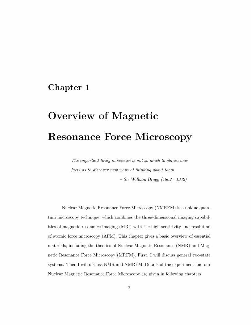
the ratio has a value of about 10 or more, will the probability reach the highest value
[MM05, Mil03]. This result is shown in Fig. 1.17. The saturation of the probability
below Pπ = 1 represents the loss of some spin following, due to inhomogeneity and
edge-of-resonance-slice effects. The cyclic adiabatic inversion condition is a very
important constraint that we need to consider during our experiment and make
sure it is well satisfied. Otherwise, the signal-to-noise ratio will be very small and
it will be hard to detect any NMRFM signal.
32

Chapter 2
MgB2: A Unique Two-band
Superconductor
It doesn’t matter how beautiful your theory is, it doesn’t matter
how smart you are. If it doesn’t agree with experiment, it’s wrong.
– Richard P. Feynman (1918 - 1988)
MgB2 is a classic example of a two-band superconductor. In this chapter I
will briefly discuss the properties of this unique superconductor. The superconduc-
tivity of MgB2 was discovered in Japan by a group of scientists in 2001 [NNM+01].
Since then there has been a huge amount of research activity on this unusual super-
conductor.
The main intriguing feature of this superconductor is that it has a supercon-
ducting transition temperature of about 39 K. This is an unusually high transition
temperature for an ordinary BCS type superconductor. Further research has re-
33

vealed that it is a Type-II, s-wave, BCS superconductor. But the most interesting
thing about MgB2 is that there are two superconducting bands: π and σ bands.
These two bands have different electron-phonon coupling strengths and may be-
come superconducting at different transition temperatures [CC03]. Among these
two bands, the σ band has a stronger electron-phonon coupling than the π band.
From the BCS theory we know that
κB Tc = 1.13 ~ωD exp[−1
V ρ(EF)
], (2.1)
where Tc is the superconducting transition temperature, ωD is the phonon Debye
frequency, ρ(EF) is the electron density of states at the Fermi level and V is the
strength of the electron-phonon coupling. It is clear from Eq. 2.1 that as the electron-
phonon coupling strength V increases, the superconducting transition temperature
Tc will also increase. It is now widely believed that the reason for the unusually
high Tc for MgB2 is the strong electron-phonon coupling in the σ band.
2.1 A Basic Introduction to MgB2
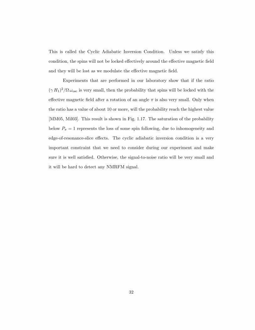
The MgB2 crystal structure and the π and σ bands of boron are shown in Fig. 2.1.
The unit cell of MgB2 consists of (orange) magnesium atoms and (blue) boron atoms.
The boron atoms form a hexagonal honeycomb lattice. The two superconducting
bands are formed by the outer electrons of boron atoms. While the (brown) σ
band is two-dimensional, the π band extends over all three dimension. Also these π
electrons connect B atoms of different layers. Since π electrons connect two different
layers, the electron-phonon coupling in this band is not that strong. However, the
σ electrons are confined within two dimensions and that makes the electron-phonon
34
Figure 2.1: a. Crystal structure and b. π and σ bands of MgB2. The orange atomsare Mg atoms and blue atoms are B atoms. The direction of c-axis is also shown. Inthe band structure, the σ band has brown color and π band has green color [CC03].
Figure 2.2: Fermi energy levels of π and σ bands of MgB2. The green section ofcolumns on four corners are Fermi surface of σ band and red tunnel with caves isthe Fermi surface of π electrons [CC03].
35

Figure 2.3: The electronic part of specific heat data for MgB2 [CC03]. The datashows clear deviation from one band BCS theory predicted curve (red curve).
coupling in this band a lot stronger than in the π band.
The Fermi surfaces created by these two bands are shown in Fig. 2.2. The
green column sections near the corners are Fermi surfaces associated with σ band
electrons while the red tunnel with caves at the center is associated with π band
electrons.
The electronic specific heat data shows the existence of two bands in MgB2,
shown in Fig. 2.3. The red curve is from a BCS theory calculation, considering only
one band. The zero field specific heat data shows clear deviation from the one band
BCS theory prediction. The deviation is especially greater at lower temperatures.
Also the slope of zero field specific heat data changes at about 10 K. It is now
believed that the σ band becomes superconducting just below 40 K. Then the π band
36

Figure 2.4: Upper critical field anisotropy of MgB2. The red lines are data frompolycrystalline sample. The green and black lines are data from two different singlecrystals. The inset shows anisotropy ration, γ = H⊥cC2/H
‖cC2, from each of these three
data sets [CC03].
may become superconducting at about 10 K temperature. Application of a small
magnetic field of about 0.5 tesla can suppress this second superconducting transition.
An externally applied magnetic field of 7 Tesla can suppress both superconducting
transitions. The electronic part of the specific heat is a clear indication of the
existence of two nearly separate superconducting bands in MgB2.
Besides the electronic specific heat measurement data, tunneling experiments
also show the existence of two gaps, and thus contributions from two bands. An-
other important aspect of MgB2 is the upper critical field anisotropy. The upper
critical field is the highest applied magnetic field below which MgB2 remains su-
perconducting. The upper critical field is much higher perpendicular to the c-axis
than parallel to the c-axis, as shown in Fig. 2.4. It is also known from the band
37

structure that electrical conduction perpendicular to the c-axis is dominated by the
σ band while that along the c-axis is dominated by the π band. The better σ-band
conductivity corresponds to a larger in-plane coherence length. The upper critical
field for H ‖ c is determined by the supercurrents perpendicular to the c-axis. So
the upper critical field along the c-axis (H‖cC2) is very small. Also, the out-of-plane
coherence length is smaller due to the weaker interlayer coupling of the π bands
of MgB2. So the upper critical field perpendicular to the c-axis (H⊥cC2) is also very
high.
2.2 Spin-Lattice Relaxation in Superconductors
One triumph of the BCS theory is that it could explain the origin of the coherence
peak in the spin-lattice relaxation process. Before I explain the origin of the co-
herence peak in the superconducting state, I will explain the spin-lattice relaxation
process in the normal state. The spin-lattice relaxation time can be measured by
an NMR experiment.
The spin-lattice relaxation process is often dominated by the hyperfine inter-
action between electrons and the nucleus. The normal state spin-lattice relaxation
rate (1/T1) due to this interaction may be expressed as follows:
1T1
=649π3 ~3 γ2
e γ2n
⟨|u2k(0)|
⟩2
EFρ2(EF) κBT, (2.2)
where ρ(EF) is the electron density of states at the Fermi level and uk is the electron
wavefunction. It is clear from the above equation that in the normal state 1/T1
decreases linearly as temperature decreases.
However, for s-wave superconductors, just below Tc a uniform energy gap
38

!!"#
""$ ""$
!!"#
!!
%&'()*+,-)-. ,/0.'1&23/1-425+,-)-.
Figure 2.5: Electronic density of states ρ(E) in normal and superconducting states.In the superconducting state, an energy gap (∆) opens up at EF and two peaksappear on either side of EF.
opens up at EF (Fig. 2.5). Since no state can exists within the energy gap, the states
within that energy interval pile up on both sides of the energy gap. As a result there
will be two peaks in the density of states, one on either side of the superconducting
energy gap. The states below the Fermi level are filled and the states above the Fermi
level are empty. So in order for nuclei to relax, they must scatter electrons from
filled states below the Fermi level to empty states above the Fermi level. However,
in the superconducting state the electrons have a phase coherence. As a result the
scattering process will not be random. Due to this coherence effect and the peaks
of the density of states on both sides of the energy gap, for most superconductors
just below Tc, 1/T1 briefly increases rapidly as temperature decreases.
Now as temperature decreases further, the superconducting energy gap also
increases [Mar00, AM01]. This is shown in Fig. 2.6. Due to this it will be expo-
nentially harder to scatter electrons from below the energy gap to above the energy
gap. Besides this, there is also less thermal excitation energy as temperature goes
39

!!"
!!
!
#$%&'"()*$"+,)-
&)&'-y/-0%/123/!
Figure 2.6: Superconductor energy gap (∆) as a function of temperature.
down. So the combined effect of all these is that 1/T1 will decrease exponentially at
low temperatures.
One effect of all this is a peak in 1/T1 versus T plot. This peak appears just
below Tc and is called the coherence peak (Fig. 2.7). The reason we call it a coherence
peak is that it is there because of the phase coherence of superconducting electrons
[Tin96]. In the normal state, there is no phase coherence of electrons and as a result
when these electrons are scattered by nuclei, there will be no coherence effects.
Below Tc, the electrons go through a phase transition and due to phase coherence
between electrons, there will be additional terms in the scattering processes. These
terms give rise to this coherence peak. This coherence peak was first explained by
the BCS theory of superconductivity and it is regarded as one the main triumphs
of the BCS theory. A coherence peak has been detected in some superconductors,
but none has been detected in the high-Tc copper oxide materials, many of which
are believed to be d-wave superconductors.
40

!"
!
!!
#$%&'&("&)*&+,
!
Figure 2.7: The coherence peak of a superconductor. The dotted line is for normalstate.
2.3 Spin-Lattice Relaxation in Polycrystalline MgB2
MgB2 is a type-II, s-wave, BCS type superconductor, so we may expect to see a
coherence peak in the spin-lattice relaxation data. The spin-lattice relaxation time
T1 of polycrystalline MgB2 was measured at different temperatures by NMR. The
data is shown in Fig. 2.8. The data shows no evidence of a coherence peak for both
magnetic fields.
It is known that many d-wave superconductors don’t exhibit any coherence
peak. However, MgB2 is not a d-wave superconductor, so our guess is that the
reason for no coherence peak in this data is due to the polycrystalline nature of
this MgB2 sample. It has already been discussed that MgB2 is a very anisotropic
material, with an upper critical field which is different along the c-axis than along
the direction perpendicular to it. Also, the Tc for this superconductor depends
on the applied magnetic field strength and its orientation with the c-axis. The
polycrystalline sample is made with many nano-size single crystals and these have
41

Figure 2.8: The spin-lattice relaxation time of polycrystalline MgB2 is plotted asa function of temperature. There is no coherence peak below Tc. T 3 slope belowTc is expected for d-wave superconductor. The data shows relaxation times for twodifferent applied magnetic fields [KIK+01].
42

all possible orientations with respect to the applied magnetic field. So due to this,
the polycrystalline specimen will have a distribution of Tc’s. That means each tiny
single crystal is becoming superconducting at a different temperature as we lower the
sample temperature. So even if the coherence peak exists for MgB2, the effect will
be averaged out over a large temperature range and we do not expect to detect it in
a polycrystalline sample. This is one probable reason for the lack of an observation
of a coherence peak in the powder MgB2 sample.
In order to see the coherence peak for the MgB2 superconductor, and to
determine the anisotropy in this and other properties, we need to measure the spin-
lattice relaxation time of a single crystal with the field along different directions.
However, the problem is that MgB2 single crystals are very small in size. The biggest
high-quality samples of MgB2 have dimensions of about 50 µm by 50 µm by 10 µm.
This is a very small sample for conventional NMR. A very sensitive conventional
NMR experiment can detect typically only about 1016 protons. For 11B nuclei, the
number of nuclei will be lot bigger since the gyromagnetic ratio of 11B nuclei is
much smaller than that of a proton. Also an NMR set-up working at this sensitivity
level has many problems. As NMR is an inductive detection technique, when the
RF coil becomes very small, it gets very hard to get a good signal-to-noise ratio.
Very recently, one group achieved MgB2 single crystal growth of ∼ 1 mm3, but no
conventional NMR detection of 11B in the superconducting state of this crystal could
be achieved [SRM+07].
However, it is possible to do a single crystal MgB2 relaxation time measure-
ment experiment with NMRFM. In fact, a single crystal of size 30 µm by 30 µm
by 5 µm will give a high enough signal-to-noise ratio to measure the 11B proper-
43

Figure 2.9: 11B NMR spectrum of the MgB2 single crystal at 81 K (H ⊥ c) showinga dipolarly split central line and two satellite lines asymmetric in shape. [SRM+07].
ties in small MgB2 single crystals at 77 K. I will talk more about the experimental
parameters required to achieve this in the next chapter.
2.4 11B NMR Spectrum of Single Crystal MgB2
Very recently Strassle et al. [SRM+07] reported the measurement of the spin-lattice
relaxation time of single crystal MgB2 in the normal state. The single crystals that
are used for their experiment are of size ∼ 1 mm3. However, they are unable to
44

measure the spin-lattice relaxation time in the superconducting state.
Figure 2.9 shows the 11B conventional NMR spectrum of the MgB2 single
crystal at 81 K. The applied magnetic field (9.047 tesla) is perpendicular to the
c-axis. The 11B NMR spectra of MgB2 is complex due to the simultaneous presence
of first- and second-order quadrupole interactions, anisotropic magnetic shift, and
nuclear dipolar coupling. The central peak exhibits a clearly visible symmetric
splitting (≈15.5 kHz) which is temperature independent. The full line width at
half maximum (FWHM) of the central peak is ≈ 8 kHz and constant in the normal
phase. However, it increases in the superconducting phase due to the inhomogeneity
of the internal magnetic field caused by the vortex structure in the mixed state.
They also measured the anisotropy of the spin-lattice relaxation time T1 of
single crystal MgB2 in the normal state. However, the worsening of the signal-to-
noise ratio caused by the diamagnetic shielding due to the onset of superconductivity
entails the need of a substantial increase of the measuring time in addition to the
necessary increase due to the slow down of the nuclear spin-lattice relaxation process,
which made it impossible for them to get reliable data on the spin-lattice relaxation
below Tc for a single crystal MgB2 by conventional NMR. But it is possible to
measure the spin-lattice relaxation time in the superconducting state of single crystal
MgB2 by NMRFM.
45

Chapter 3
Experimental Details and
Results
A theory is something nobody believes, except the person who made it.
An experiment is something everybody believes, except the person who made it.
– Albert Einstein (1879 - 1955)
Nuclear Magnetic Resonance Force Microscopy (NMRFM) is a novel scanned
probe which holds potential for atomic-scale resolution. This technique has potential
applications in many different fields. In this chapter, I will discuss various aspects
and instruments used to do the NMRFM experiment. This chapter also includes
details of fiber optic interferometry, signal-to-noise calculations, difficulties of the
experiment, signal artifact, etc. I also will discuss the experimental results that I
have obtained so far.
46

Magnet
z
x
MgB2 single
crystal
RF Coil
Fiber Optic
InterferometerResonance Slice
Cantilever
Figure 3.1: My NMRFM experiment setup.
3.1 Experiment Setup
Figure 3.1 shows my NMRFM experimental setup. A micron size MgB2 single
crystal is mounted on an ultra-floppy cantilever. The size of our samples are on the
order of 40 µm by 40 µm by 5 µm and are mounted on the cantilever with silver
epoxy. During sample mounting, we have to be very careful so that we don’t use
too much epoxy. If excess epoxy is used, then the mass of the cantilever increases
to a limit where the resonance frequency will be very low, sacrificing sensitivity
(Fmin ∝ 1/√ωosc). Also, after mounting the samples, we need to bake the system at
about 60C for a few hours. We also need to be careful that epoxy chemicals don’t
wet the cantilever. If any chemical wets the cantilever, it will change the spring
constant of the cantilever. The quality factor of the cantilever will also decrease,
47

Figure 3.2: SEM image of one cantilever used for NMRFM experiment.
especially at low temperature. Besides all this, we should keep in mind that MgB2 is
an anisotropic crystal. So during the sample mounting, we need to carefully mount
the sample so that c-axis of the crystal is parallel or perpendicular to the external
magnetic field. For our initial experiments, we chose H ‖ c, since then the somewhat
flat resonance slice is parallel to the crystal, improving the signal-to-noise ratio.
One of the cantilevers used for this experiment is shown in Fig. 3.2. These
are about 100 µm long, with a square head at the top. The head dimension is about
20 µm by 20 µm. The cantilever arms are 5 µm wide and only a few tenths of a
micron (about 300 nm) thick. The spring constant of these cantilevers is about 10−2
N/m, which is measured by a thermal noise scan. These cantilevers are fabricated
lithographically on single crystal silicon [CMM+04]. The sample is mounted on one
face of the square head of the cantilever. The laser light is pointed at the opposite
face of the square head of the cantilever. All cantilevers are attached to a large
silicon substrate, which is in turn attached to the probe.
The entire experiment is done inside a large superconducting magnet, which
48

produces a uniform 8.067 tesla magnetic field. In addition to the static magnetic field
~H0, there is also a field-gradient-producing magnet. This is a small iron cylinder,
placed very close to the sample. The total magnetic field is shown in Fig. 1.15.
The total magnetic field changes over distance and this gives the spatial resolution
of NMRFM. For higher spatial resolution, or a smaller resonance slice, we need a
higher field gradient. Calculations show that a nanomagnet can provide enough field
gradient to image a single proton. Appendix B has details of this calculation and
its results. The program that I wrote to calculate the 3D magnetic field profile and
field gradient is included in Apprendix A. The magnetic field created by a 2 micron
radius, 180 nm long cylindrical permalloy magnet is shown in Fig. 3.3.
Another important component is the RF coil. This coil produces a radio
frequency field when an alternating current flows through it. The RF coil is part
of an RF tank circuit, which is tuned to have a total impedance of 50 Ω using a
network analyzer. The output impedance of the RF power amplifier is matched to
50 Ω. So in order to maximize power transfer from the RF amplifier to the RF coil,
the tank circuit impedance also should be close to 50 Ω.
3.1.1 Fiber Optic Interferometer
Another very important part of the NMRFM experiment is the fiber optic inter-
ferometer and related circuit, used to detect any vibration of the cantilevers. A
schematic of the fiber optic interferometer is shown in Fig. 3.4. A laser diode is
used as the light source. The output of the laser diode goes to a directional coupler,
which rejects 90% of the laser light and only 10% of the laser light goes towards the
cantilever. The reason for this is that if too much laser light hits the cantilever, then
49

Distance along axis (micron)
Hz (
T)
Hz (
T)
Figure 3.3: Magnetic field created by a 2 micron radius, 180 nm thick cylindricalpermalloy magnet. The second plot shows contours of constant magnetic field lines.The axis of this cylinder is along the z direction. This data is calculated by a Cprogram that is given in Appendix A. Then the data is plotted by using Matlab.
50

Stack
Piezo
Diode
Laser
Directional
Coupler
Fiber
Stage
!
Feedback
Circuit
Lock-in
Amplifier
Filter
High Freq.
SignalLow Freq.
Signal
Rejected
Cantilever
with a sample
Fiber Optic Interferometer
Interference
PatternPhoto
Diode
Current-to-Voltage Converter
Figure 3.4: Fiber optic interferometer and related circuits.
it will heat the cantilever. Part of the light gets reflected backward from the fiber
edge and the rest gets transmitted through it. Much or all of the transmitted light
gets reflected by the cantilever; some of this reflected light re-enters the fiber and
interferes with the light reflected from the edge of the fiber. These two rays have
a path length difference of 2∆ and as a result they create an interference pattern.
As the cantilever vibrates, this path length changes and hence the interference pat-
tern also changes. This interference pattern intensity is a periodic function of the
fiber-cantilever distance, with a period length that is half of the wavelength of laser
diode.
The interference pattern travels through the fiber and hits a photo diode.
This photo diode coverts the time dependent light intensity signal to an alternating
current. As the interference pattern changes, the photo diode output current also
51

changes. This current in turn gets converted to a voltage and this is our signal. This
signal then passes through a filter and the low-frequency part of the signal goes to
a feedback circuit. This feedback circuit controls a stack piezo, which controls the
movement of the fiber stage. I will discuss it below, after discussing signal processing
near the mechanical oscillator frequency.
3.1.2 Lock-in Amplifier
The high-frequency part of the signal goes to a lock-in amplifier, which digitizes the
signal. The lock-in amplifier is a phase sensitive device, which can determine the
relative phase of different cantilever modes. The lock-in also amplifies and mixes
down to near dc the Fourier components of the signal within a given bandwidth.
The bandwidth (∆ν) of the lock-in amplifier is related to its time-constant (τc) by
the following relation: ∆ν = 1/4 τc for the normal 6 dB/octave filter. The reference
signal frequency for the lock-in is usually set to the resonance frequency of the
cantilevers. The lock-in used in this experiment was a Stanford Research Systems,
model SR 830 DSP lock-in amplifier.
This lock-in amplifier has two outputs. Both of these outputs go to a Nicolet
model Pro30, a digital signal recorder, which records and averages these signals.
This data is then analyzed to detect the NMRFM signal. The outputs of the lock-in
amplifier are usually set to provide the amplitude R and the phase Θ of the signal.
We also can select X and Y , the elastic and absorptive parts of the signal, respec-
tively. The lock-in can also be controlled by a computer program. We have written
a LabVIEW program to automate these steps. This lock-in amplifier was also used
to determine the cantilever characteristics, which I have discussed in Section 3.2.
52

3.1.3 Fringe Lock
Due to various reasons, the gap between the fiber and cantilever may change. One
possible reason is temperature variation. This will cause a change in the DC signal.
Also there are many sources of low frequency vibrations. These low frequency noises
will change the DC level and create some low frequency noise. In order to cancel
these, we use the low-frequency part of the signal as an input to a feedback circuit.
The details of the feedback circuit are given in C. W. Miller’s Ph.D. thesis [Mil03].
The output of this feedback circuit is directly connected with a stack piezo which
moves the fiber to cancel out these slow changes.
Besides damping out the low frequency noise, the feedback circuit is used to
lock onto the interference pattern or fringe. It is known that if the distance between
the fiber and the cantilever is changed, we will see a shift in the position on the
interference pattern. In order to get the best force sensitivity, we need to lock the
interference pattern at the point of maximum slope. Only then a small vibration of
the cantilever will induce the largest voltage change. The absolute value of the slope
is maximum at the half way between points of maximum and minimum intensity of
the interference pattern. The slope at that point is given by∣∣∣∣dVdz∣∣∣∣max
' π
2× 4λ× (Vmax − Vmin), (3.1)
where λ is the wavelength of the laser, V is the interference voltage signal, z is the
distance between the fiber and the cantilever, and Vmax and Vmin are the maximum
and the minimum intensities of the interference pattern, respectively. Using an
adjustable DC power supply, we apply a DC voltage to the stack piezo to set the
fringe at the point of maximum slope. Then the fringe lock feedback circuit is
switched on to keep the fringe at that position.
53

Figure 3.5: A picture of my probe.
The above equation can also be used to convert the voltage signal to a vi-
bration amplitude of the cantilever. If the voltage difference between the highest
and the lowest points of the interference pattern is Vpp (= Vmax − Vmin), then the
amplitude of cantilever vibration, x, is
x ≈ λ
2π VppV, (3.2)
where V is the signal amplitude at the resonance frequency of the cantilever. The
wavelength (λ) of diode laser is 1310 nm for our experiment. The amplitude of
cantilever vibration is usually a few nanometers. We have selected this diode laser
to minimize the cantilever heating. The wavelength of this diode laser falls within
the band-gap of silicon. As a result, (ideally) no laser light will be absorbed by the
silicon-made cantilever.
54

3.1.4 Other Accessory Systems
Another very important component of the experiment is the large 8.067 tesla mag-
net. It is a Cryomagnetics, Inc. superconducting magnet, which produces a uniform
magnetic field, with 1 ppm homogeneity over 1 cm3 volume. We also have a vacuum
pump to pump out the air from the probe. The air pressure inside the probe is
about 10−5 torr. It is mainly to reduce air damping of the cantilever vibration. In
normal atmospheric pressure, damping is so large that the quality factor Q of the
cantilever vibration is very small. Only at very low pressures does the cantilever
have a large amplitude of vibration. However, during low temperature experiments,
we put a small amount (a few mTorr) of helium gas inside the probe. This helium
acts as an exchange gas to conduct heat to the outer cryogen bath and maintains a
low temperature within the probe.
Another very important component is the low temperature system. In order
to do the NMRFM experiment, we need to cool down the probe to very low temper-
atures. It was shown above that the signal-to-noise ratio increases as temperature
decreases, mainly due to lower thermal noise and greater magnetization at lower
temperatures. MgB2 also becomes superconducting at about 39 K. Such tempera-
tures are attained with a dewar. We use a Janis cryostat, model SVT-200T, the tail
of which is specifically designed to fit into the 3.50′′ diameter bore of our magnet
and is equipped with a Lakeshore, model CX-1050 calibrated Cernox thermometer
located at the bottom of the sample space. The inner space of the dewar is filled
with liquid helium, while the outer space is filled with liquid nitrogen; a layer of
vacuum thermally isolates each space. When the probe is placed inside a third iso-
lated space, the central sample space of the dewar, it is surrounded by cold helium
55

gas to vary the temperature, or by liquid helium to reach 4 K.
In the probe there are three different stages to move the cantilever on the
X-Y plane, move the magnet towards the cantilever and move the fiber towards
the cantilever. All these stages are used to make very accurate alignment of fiber,
cantilever and magnet. Since the cantilever head is only 20 micron wide, we need
very good alignment to do this experiment. Also without proper alignment, the
interference intensity will not be strong and without a strong interference intensity
we will not be able to get a large voltage signal.
3.2 Determining Cantilever Characteristics
The resonance frequency and and quality factor of the cantilever first has to be
determined before doing the NMRFM experiment. Also we need to find out the
spring constant of the cantilever to calculate sensitivity of NMRFM experiment.
3.2.1 Frequency Scan
During the frequency scan, a sinusoidal voltage is applied for a time interval ∆t
from a Stanford Research System DS345 signal generator to a piezo plate on which
the cantilever is mounted. A reference signal from the signal generator goes to the
reference input of the lock-in amplifier. The applied voltage causes the ceramic piezo
(made by American Piezo Ceramics, Inc.) to expand or contract by an amount ∆h
according to the formula
∆h = d33 V, (3.3)
where d33 is a piezo-dependent constant equal to 2.9 × 10⁻¹⁰ m/V and V is the
applied voltage. The silicon chip containing the cantilevers is glued to the piezo
56

Frequency (Hz)
Sig
nal A
mplitu
de (
Volt)
Figure 3.6: Frequency scan of a cantilever with a MgB2 crystal. Blue line is themeasured signal and red line is the best fit curve. From the Lorentzian fitting we getthe resonance frequency 721 Hz and the quality factor about 450. Pressure insidethe probe: less than 1 millitorr and frequency step size: 0.5 Hz.
by silver epoxy (H21D of Epoxy Technology). So if we apply a periodic voltage,
that will induce periodic expansion of the piezo. This will impose a driving force
on the cantilever at the frequency of the voltage. Due to cantilever vibration, the
interference pattern also will change periodically and it will induce a periodic voltage
signal. This signal is sent to the lock-in where it is averaged with a time constant
τc. The cantilever shaking interval ∆t is set to be 3 times τc to ensure the output
of the lock-in is stable.
The equivalent noise bandwidth of the lock-in is ∆ν = 1/4τc when the normal
6 dB/octave filter is used. This means that the lock-in is effectively detecting all
signals within the frequency range f0−∆ν to f0 + ∆ν. After shaking the cantilever
for ∆t time, the program saves the lock-in outputs X and Y in the computer and
57

then increments the frequency of the signal generator and then repeats all of these
steps. This is known as frequency scan.
After the frequency scan, the cantilever vibration amplitude is plotted for
different frequencies. When the frequency of vibration is the same as the resonance
frequency of the cantilever, the amplitude will be a maximum. So by fitting the
amplitude versus frequency plot to a Lorentzian, we can determine the resonance
frequency of the cantilever and this also gives a decent estimate of the quality factor,
Q (Fig. 3.6). We have seen seen that Q increases as pressure drops. In fact in order
to get a decent Q we need to keep the pressure of the probe at a level of few mTorr.
3.2.2 Determining the Cantilever Spring Constant
Another very important characteristic of the cantilever is its spring constant. While
we don’t need to know the exact spring constant of the cantilever to perform the
NMRFM experiment, we must know the approximate value in order to calculate
the signal-to-noise ratio. Without a decent signal-to-noise ratio, it is impossible to
detect any signal without much signal averaging.
Direct measurement of the spring constant, κosc, is not easy for such micron
size cantilevers. However, it is possible to determine κosc using the Equipartition
Theorem, which is12κosc 〈x2〉 =
12κB T, (3.4)
where 〈x2〉 is the mean square noise vibration amplitude of the cantilever and T is
temperature. But determining 〈x2〉 is not that straightforward. It is defined as
〈x2〉 =∫ ∞
0|G(f)|2 Sf df, (3.5)
58

where G(f) is the mechanical transfer function of the cantilever and Sf is the noise
spectral density. The absolute square of mechanical transfer can be written as
|G(f)|2 =f4
osc/κ2osc
(f2osc − f2)2 + (foscf/Q)2
, (3.6)
and the noise spectral density is given by
Sf =4κosc κB T
2πf Q. (3.7)
The lock-in itself measures the RMS noise vibrations√|G(f)|2 Sf with a bandwidth
∆ν. So selecting a very narrow lock-in bandwidth will allow us to reconstruct the
shape of√|G(f)|2 Sf by determining the RMS values for discrete frequencies in the
spectrum.
In order to determine the RMS noise amplitude for a given frequency, a
time series must be taken by digitizing the outputs of the lock-in for a given fre-
quency. The RMS value of this time series will be the RMS noise amplitude for
that frequency. When these RMS values are plotted for different frequencies, we
get the RMS noise amplitude spectrum. The noise power spectrum (the integrand
of Eq. 3.5) is calculated by squaring the RMS noise amplitude spectrum, and then
dividing the result by the bandwidth of the lock-in amplifier. The resulting curve is
then integrated over the frequency range to get the value for 〈x2〉. Now using Eq. 3.4
we can calculate κosc. An example of RMS noise amplitude, power spectrum and
corresponding integrated power spectrum of a cantilever at room temperature is
shown in Fig. 3.7. It is also possible to write a LabVIEW program to do all of these
steps automatically and find the cantilever spring constant. The cantilevers used in
this experiment have spring constant of about 2.0× 10⁻³ N/m.
59

Figure 3.7: An example of RMS noise amplitude, power spectrum and correspondingintegrated power spectrum of a cantilever at room temperature. The lock-in timeconstant is set at 3 second and the reference frequency increment step is 0.1 Hzbetween different time series [Mil03].
60

!0
RF
Fie
ld F
requ
ency
Time
!CAdI Trig0 Trig1 Trig2
Figure 3.8: The RF frequency modulation scheme is shown here. τCAdI is theduration of Cyclic Adiabatic Inversion or frequency modulation.
3.3 NMRFM Experiment
NMRFM is a very complex experiment with several components. I have described
the fringe lock system, fiber optic interferometer, RF coil, gradient producing mag-
net, cantilever, etc. Also, I have described how to oscillate the sample magnetization
by modulating the RF field frequency. Now I will describe the RF field frequency
modulation setup and related electronics. After that I will talk about the way we
do the NMRFM experiment in our laboratory.
3.3.1 Frequency Modulation Setup
As we have discussed before, in order to create an oscillating magnetization, we
need to modulate the RF frequency. However, we can not start modulating the RF
61

frequency instantaneously. If we do so, we will not be able to lock the spins around
the effective magnetic field in the rotating frame. There are several ways to start the
RF frequency modulation. The way I did that for my experiment is to start with an
RF field frequency that is far from the resonance frequency ω0, then exponentially
approach the resonance frequency ω0, and then start modulating the RF frequency.
The RF frequency modulation amplitude is 50 kHz and its frequency is the resonance
frequency of the cantilever. After a duration, the frequency modulation is stopped
and RF frequency goes back to far off resonance value. This frequency modulation
scheme is shown in Fig. 3.8. The electronics for achieving this is described in detail
in Casey W. Miller’s Ph.D. thesis [Mil03].
3.3.2 RF Power Amplifier
The output power from the RF signal generator is very low, usually order of few
milliwatt. To achieve a value of H1 (≥ 10 gauss) adequate for manipulating nuclear
spins, we need to amplify the signal. This is done by an RF power amplifier. We use
an ENI model 5100L-NMR RF power amplifier to amplify the RF signal by 50 dB.
The output of this RF amplifier goes to the tank circuit, which contains the RF coil.
The output impedance of the RF power amplifier is 50 Ω. That is why we also tune
the impedance of tank circuit to 50 Ω. This will ensure maximum power transfer
from the amplifier to the coil and we will get a large RF magnetic field.
To do the MgB2 NMRFM experiment, it is very important that we get a
large RF magnetic field for two reasons. First, the RF field must be larger than the
local fields inside the sample. For solids dense with many nuclei, it is known that
local fields are large, on the order of a few gauss. So the external RF field must
62

be greater than the local fields, or the RF field will not be able to modulate the
spins. The second reason is that we have to satisfy the cyclic adiabatic inversion
condition (Eq. 1.54). According to that condition, a sufficiently large RF magnetic
field is needed to achieve adequate adiabatic following, and thus an adequate signal-
to-noise ratio. For our desired Ω = 50 kHz and a typical fosc = 0.7 kHz, the cyclic
adiabatic inversion condition requires (γ H1)2/(Ωωosc) > 10, which gives H1 > 14
gauss. It is typically necessary to get at least 10 gauss or more RF field strength.
3.3.3 Signal-to-Noise Ratio Calculation
Before performing any experiment, it is necessary to calculate the theoretically ex-
pected signal-to-noise ratio of that experiment. It is wise to do the experiment only
when we have a decent signal-to-noise ratio. For our experiment, we want to detect
11B nuclei, with spin S = 3/2. The gyromagnetic ratio for 11B is γ/2π = 13.66
MHz/T. Our magnetic field gradient is 200 T/m (based on the calculation given
in Appendix A) and our chosen RF modulation amplitude is 50 kHz. Choosing
Ω ∼ 2γH1 ensures that the magnetization is oscillated with nearly maximal ampli-
tude. (See Fig. 1.13). Using Eq. 1.53, we get the resonance slice thickness of about
31 µm. However, our sample thickness is only about 10 microns. So that means the
effective resonance slice thickness for our experiment is only 10 microns. Recall a
typical MgB2 single crystal area is about 40 microns by 40 microns.
Other experimental parameters are: total magnetic field H0 = 8.28 tesla,
MgB2 density: 2.57 g/cm3, molecular weight: 45.93 g/mole and natural abundance
of 11B nuclei: ∼ 81%. Parameters related to the cantilever are: κosc ≈ 2 × 10⁻³
N/m, ∆ν = 2.5 Hz, Q ' 100, fosc = 740 Hz.
63
From Eq. 1.51 we get that at temperature T , the magnetic force on the
cantilever Fmag = 5.6 × 10⁻¹²/T Newton. Also from Eq. 1.50 we get that at tem-
perature T , the minimum detectable force by a cantilever is Fmin ≈ 0.7× 10⁻¹⁵√T
Newton. Clearly the signal-to-noise ratio depends on temperature. At liquid nitro-
gen temperature, 77 K, the signal-to-noise ratio is Fmag/Fmin ∼ 11. We feel this
was a sufficient theoretically expected signal-to-noise ratio to start the experiment.
Actual signal-to-noise ratio is usually slightly less than this as there can be other
sources of noise and errors.
3.4 Challenges of NMRFM Experiment
We had to overcome several challenges to perform the NMRFM experiment. One
of the main challenges with this experiment is sample mounting. Since MgB2 is a
anisotropic sample, so we have to mount the sample very carefully. We have an
8 tesla magnet; so to measure the relaxation times in the superconducting state,
our external magnetic field must be perpendicular to the c-axis of the MgB2 single
crystal. Unfortunately, our experimental setup requires that we mount such a sample
vertically (on edge) on the cantilever. I have discussed some details of the sample
mounting on the Section 3.1. We also have to be very careful during the sample
mounting so that we don’t accidentally break a cantilever. It requires a lot of
practice and patience to mount a sample properly on a cantilever. We use a very
stable XYZ movement stage to do that.
Other major issues with this probe are problems at low temperature. We have
performed all our experiments at 77 K. And we have faced several challenges at that
temperature. First of all is the alignment of the cantilever with the fiber. We align
64

those at room temperature. Then we cool down the probe to 77 K. However, due
to differential contraction of different probe elements, very soon all this alignment
is lost. In fact, many things may happen. Sometimes the fiber had destroyed the
cantilever. Also the fiber may point in a different direction than at the cantilever.
If that happens, we will not have any interference signal. In that case, and if our
lateral movement could not re-attain alignment, we have to pull the probe out and
realign the fiber-cantilever and go through all those steps again. It usually takes
three to four tries to get correct fiber-cantilever alignment. Also in order to avoid
fiber destroying the cantilever, we usually pull the fiber away from the cantilever
during cool-down, and then advance it when cool.
Also we have seen that at low temperature, the gears get jammed. In order
to avoid that I had to clean the gears very often and also made sure that all bolts
are tight. Also when we place the probe inside the magnet, the large magnetic field
pulls the probe towards itself. So that may also destroy the cantilever if the fiber
points at it at that time. So in order to avoid that, I used to point the fiber at some
other laterally displaced direction during this. Only when the probe is inside the
magnet, I align the fiber with the cantilever.
Another problem is associated with the feedback piezo. The type of piezo
that we have used in this probe works well only at room temperature. However,
when we cool down the probe to 77 K, the plastic packaging of the piezo will harden
and as a result, the piezo may not be able to expand/contract at low temperature.
In fact, these piezos become unusable after few cooling-heating cycles. Although the
ceramic piezo works at very low temperature, the pressure from plastic packaging
makes those completely ineffective at low temperature. As far as I know, there is
65

only one German company which makes piezo that can be used at low temperature.
3.5 Results and Discussion
There are several ways to do an NMRFM experiment. In my experiment, I have
fixed the resonance frequency ω0 at 112.18 MHz. We also know that only those nuclei
which are within the resonance slice will exert a force on the cantilever. The center
of the resonance slice is at the point where total magnetic field is Htot = ω0/γ = 8.28
tesla and the width of this slice is 2Ω/γ∇Hz ≈ 31 microns. Due to the presence of
the gradient field producing magnet (a 2.1 mm diameter, 20 mm long iron cylinder),
the magnetic field is changing over distance. Since we have fixed the radio frequency,
this also fixes the distance between the resonance slice and gradient field producing
magnet, which is about 1.5 mm for this experiment (Fig. 3.1). This experiment was
performed at 77 K.
Initially I placed the iron magnet far from the sample and then very slowly
I decreased the distance. Our setup allows us to decrease the distance by about
3-micron steps. When the resonance slice does not penetrate the sample, the am-
plitude of cantilever vibration is small. The cantilever rings up to a frequency-
independent value due to strong coupling of the modulated RF field with the can-
tilever; this “artifact” has an amplitude of about 1.9 nm in Fig. 3.9. Fluctuations
about this baseline are due to thermal noise. However, when the resonance slice
penetrates through the sample, the amplitude of cantilever vibration increases. As
we decrease the sample-magnet distance further, the resonance slice will be out of
the sample and the amplitude of cantilever vibration will again decrease to the arti-
fact and thermal noise value. This is shown in Fig. 3.9. The “dips” of the amplitude
66

1480 1485 1490 1495 1500 1505 1510 1515 1520 1525 1530 15350.5
1
1.5
2
2.5
3
3.5
4MgB2 NMRFM Signal
Magnet!Cantilever Distance (µm)
Can
tile
ver
Vib
rati
on A
mp
litu
de
(nm
)
Figure 3.9: NMRFM signal of 11B nuclei in MgB2 sample.
on either side of the peak is probably due to the magnetic field fringing effects.
The amplitude of cantilever vibration induced by the nuclear magnetism is
approximately 2.2 nm. This corresponds to a magnetic force of
Fmag =κosc · xmag
Q≈ 2× 10⁻³ N/m · 2.2× 10⁻⁹ m
100= 4.4× 10⁻¹⁴ N, (3.8)
which is slightly smaller than the theoretically expected value (Eq. 1.51) of 0.7 ×
10−13 N at 77 K. This theoretical overestimation may be due to several reasons.
First, we don’t know the exact size (both thickness and area) of the MgB2 single
crystal. Second, the cyclic adiabatic inversion condition (Eq. 1.54) is probably not
properly satisfied. Third, we don’t know the exact value of the magnetic field
gradient. We also don’t know the exact value of the cantilever spring constant.
67

Similarly the rms thermal noise motion is about 0.5 nm, corresponding to
Fnoise =κosc · xnoise
Q≈ 1.0× 10⁻¹⁴ N, (3.9)
again slightly larger than the theoretically estimated value (Eq. 1.50) of 0.6×10⁻¹⁴ N
at 77 K. This theoretical underestimation is probably due to the approximate value
of the cantilever spring constant used, ∼ 2 × 10⁻³ N/m. So the experimentally
determined signal-to-noise ratio for my NMRFM experiment is about 4.4, which is
less than half of the theoretically estimated value (Eq. 1.52) of about 11 at 77 K.
3.6 Future Studies
This is the first force detected NMR signal of 11B nuclei. I have demonstrated that
it is possible to detect 11B nuclei by NMRFM. Thus it is reasonable to undertake
future NMRFM experiment on 11B in MgB2. In the future, we will study the spin-
lattice relaxation rate anisotropy in both normal and superconducting states, the
two-band effects on the relaxation process and the existence of any coherence peak
(or two peaks?!!) in the superconducting state of a single crystal MgB2 sample.
68

Chapter 4
Ti-sheathed Doped MgB2
Superconducting Wires
Nothing shocks me. I’m a scientist.
– Harrison Ford (1942 - ), as Indiana Jones
The principle goal of this separate project is to study the superconducting
properties of SiC doped Ti-sheathed MgB2 wires. In contrast with the previously
reported results that nano-SiC doping with a doping range below 16 wt% usually
enhances the critical current density Jc, particularly at higher fields, our measure-
ments show that SiC doping decreases Jc over almost the whole field range from
0 to 7.3 T at all temperatures. Furthermore, it is found that the degradation of
Jc becomes stronger at higher SiC doping levels. Our results indicate that these
negative effects on Jc could be attributed to the absence of significant effective pin-
ning centres (mainly Mg2Si) due to the high chemical stability of the crystalline-SiC
69

particles [LFL+07]. Here I will give details of the sample preparation, experiments,
and results. I also will discuss in detail the probable reasons for the observed results.
4.1 Introduction
Following the first report of Dou et al. on the dramatic enhancement of critical
current density (Jc) in MgB2 superconductors by nano-SiC doping, extensive studies
have been carried out on nano-SiC-doped MgB2 wires/tapes/pellets prepared with
different SiC grain sizes (5300 nm), doping levels, sintering conditions and precursor
powders [DSH+02]. In particular, the dependence of Jc on the SiC doping level is
an important issue and has been studied by a number of groups in the last few
years. The initial study of Dou et al. on Fe-sheathed MgB2(SiC)y samples, with
y being the weight percentage of SiC and the size of SiC in the range between
10 and 100 nm, indicated that Jc increases dramatically with y increasing from
0 to 10 wt%. However, it is still unclear at what doping level and under what
synthesizing/fabricating conditions (e.g. sintering temperature and time, etc.) SiC
doping would optimize or degrade Jc.
Recently, Liang et al. have have successfully fabricated Ti-sheathed, undoped
MgB2 wires with high Jc and demonstrated that the performance of a Ti-sheath on
Jc is comparable to or even better than an Fe-sheath [LFH+06]. To further increase
Jc for future applications of Ti-sheathed MgB2 wires in lightweight superconducting
magnets, we obtained from Liang Ti-sheathed MgB2 wires doped with crystalline
nano-SiC (20 nm) at different doping levels. We wanted to know if Jc in these
wires could be enhanced substantially and the results obtained could help us further
understand the dependence of Jc on the SiC doping level.
70

4.2 Experimental Details
Ti-sheathed, SiC-doped monocore MgB2 wires were fabricated using the standard
in situ powder-in-tube (PIT) method. The SiC powder was well mixed with the
milled Mg + 2B mixture which has an average particle size of about 1 µm. The
SiC powder with a nominal size of 20 nm was purchased from Alfa Aesar. The
MgB2(SiC)y wires were prepared with SiC doping levels at y = 5, 10 and 15 wt%.
Wire sections about 6 inches long were cut from the as-drawn wires and sintered
in a tube furnace in flowing high purity argon with the following schedule: the
temperature was increased from room temperature to 800C at a rate of 300C h−1,
kept at 800C for 30 min, and then cooled down to room temperature at a rate of
100C h−1. The cross-sectional areas of the wires were about 1 mm × 1 mm and
the MgB2 cores had cross-sectional areas of about 0.34 mm × 0.37 mm.
The size and shape of the commercial SiC particles were measured by trans-
mission electron microscopy (TEM). The impurities, compositions and microstruc-
tures of the SiC-doped MgB2 wires were studied by TEM, x-ray energy dispersive
spectroscopy (EDS) and scanning electron microscopy (SEM). The temperature (T )
dependent resistivity, ρ(T ), was measured by a standard four-probe dc technique.
The temperature dependent magnetization, M(T ), was measured in both zero-field-
cooled (ZFC) and field-cooled (FC) modes using a magnetic properties measurement
system (MPMS) magnetometer from Quantum Design. Except for the 30 K hys-
teresis half-loop of the sample with y = 10 wt% SiC, which was measured using the
MPMS, all of the other hysteresis loops were measured using a vibrating sample
magnetometer (VSM) with a field ramping step of ∆H ≈ 33 Oe. In the M(T ) or
M(H) measurements, the longitudinal axis of each wire sample was oriented along
71

Figure 4.1: XRD patterns for the core materials of the Ti-sheathed, SiC doped MgB2
wires. For comparison, XRD patters of three reference compounds, SiC powder,MgB2 powder and Ti powder, are shown [LFL+07].
72

d
c e
(a) (b)
Figure 4.2: (a) TEM imag of the powder of the 20 nm SiC-doped MgB2 core with adoping level of 10 wt%. (b) The magnified bottom portion of image in (a). (c)-(e)The EDS spectra taken sites of the sample [LFL+07].
the direction of the applied magnetic field.
4.3 Results and Discussion
The average size of SiC particles was measured as 20.2 nm with a standard devi-
ation of 9.7 nm. The X-ray diffraction (XRD) pattern shown in Fig. 4.1 indicates
that these SiC nanoparticles are crystallized in the cubic β-SiC phase and lattice
constant a = 4.362(4) A. Figure 4.1 shows the XRD patterns for the core material
of the MgB2(SiC)y wire samples, with the SiC doping level (in weight percentage of
73

MgB2) y = 0, 0.05, 0.10 and 0.15. For comparison, the patterns of three reference
compounds, SiC (20 nm), MgB2 powder (-325 mesh) and Ti powder (-325 mesh),
are also shown in Fig. 4.1. All of the patterns are normalized to the intensity of
the strongest peak in each pattern. The major peaks for these wire samples can be
indexed with the MgB2 hexagonal structure, indicating that the core materials in
these wires are primarily the MgB2 phase. The SiC(111) peak located at 2θ ≈ 35.6
is seen in each pattern of the three SiC-doped samples but not in the undoped
sample (y = 0) indicating that the SiC nanoparticles did not react completely with
the other elements during the 30 min sintering at 800C. However, our XRD data
cannot determine definitely the existence of Mg2Si impurities in the samples.
In Fig. 4.2, we show the TEM images and EDS spectra for the powder
of the core material of the MgB2 wire with 10 wt% SiC doping. Figure 4.2(a)
shows an overview image in lower magnification, and its bottom part is magnified
in Fig. 4.2(b). The large grains are identified mainly in the MgB2 phase, as shown
by the EDS analysis in Fig. 4.2(c). Some particles of irregular shape are identified
as amorphous SiO2; an example is marked in Fig. 4.2(a) and its EDS spectrum is
shown in Fig. 4.2(d). Figure 4.2(b) shows that on the surface of MgB2 grains there
is a distribution of two kinds of particles: the larger ones (darker) with size 17.1±3.5
nm are SiC, and the well dispersed smaller particles with size less than 10 nm are
MgO particles. Because these two kinds of particles are well dispersed, the EDS
spectrum shows both MgO and SiC in Fig. 4.2(e). The EDS does not detect the
existence of Mg2Si particles, indicating that either Mg2Si impurities were not formed
in the SiC-doped samples during the sintering process or their concentration is too
low to be detected. This EDS result is consistent with the XRD result discussed
74

above and can be explained by the slight reaction of SiC and the formation of SiO2
which reduces the amount of Si available for forming Mg2Si.
The above XRD/TEM/EDS results show some distinct differences between
our SiC-doped MgB2 samples and those of Dou et al. For our samples, the reaction
between the doped SiC particles and Mg + 2B mixture is very slight, as seen by
the small size change for the SiC particles before and after sintering, whereas for
their samples, SiC reacted fully and no SiC peak was observed in the XRD patterns.
For our samples, no indication of the formation of significant or detectable amounts
of Mg2Si nanoparticles was observed. For their samples, a prominent intensity of
Mg2Si peak was observed in the XRD patterns. Our TEM result shows that the SiC
particles are mostly located on the surface boundaries of the MgB2 grains, whereas
their TEM results indicated that most of the SiC particles are embedded inside the
MgB2 grains.
Shown in Fig. 4.3 are the SEM images for the cores of the four wire samples.
The surfaces of the samples were polished. These images show that large numbers of
holes/voids exist in the samples. Most of them are about 12 µm in diameter which is
close to the size of the Mg particles in the milled Mg + 2B powder precursor. These
voids could be produced by the volume reduction in the Mg + 2B→MgB2 reaction,
it could also be partially attributed to the evaporation of the Mg particles during
the sintering of the wires. It appears from the SEM images that the density of the
holes/voids decreases with the increase in the doping level. For example, the hole
density for the 15 wt% SiC sample shown in Fig. 4.3(d) is much less than that of
the undoped sample shown in Fig. 4.3(a). In the process of mixing and packing the
Mg, B and SiC powders, the spaces between the bigger Mg + 2B particles (∼1 µm
75

(a) (b)
(c) (d)
Figure 4.3: SEM images of the cores of the Ti-sheathed MgB2 wires which are (a)undoped, (b) doped with 5 wt% SiC, (c) doped with 10 wt% SiC and (d) dopedwith 15 wt% SiC. The surfaces of the cores were polished before taking the images.These SEM images show that a large number of holes/voids exist in the cores of thewires [LFL+07].
in size) were filled by the much smaller SiC nanoparticles (20 nm average size), thus
a higher doping level of SiC could result in a higher filling or packing factor.
Figure 4.4 shows the magnetic hysteresis loops obtained for the various sam-
ples at different temperatures. Figure 4.5 shows the field dependent magnetic Jc(H)
curves for the Ti-sheathed MgB2(SiC)y wire samples. The rectangular cross sections
of the MgB2 wire cores are 0.34 mm × 0.37 mm = 0.126 mm2 and the lengths of the
wires range from 7.5 to 10 mm. The magnetic Jc of the samples was calculated with
the formula Jc = 20 ∆M/[a(1 − a/3b)] from the Bean critical state model, where
∆M is the difference between the upper and lower branches of the hysteresis loops
(Fig. 4.4), a = 0.34 mm and b = 0.37 mm. Here we want to calculate the critical
current density of MgB2 wires and that is the reason for choosing those values for
parameters a and b. Our field dependent magnetization measurement on the Ti-
76

Figure 4.4: Hysteresis of undoped and doped MgB2 wires, measured by a vibratingsample magnetometer. This data is used to calculate Jc using the Bean model. Insetof (c): this data only was taken using a SQUID magnetometer [LFL+07].
77

sheath of the wires indicates that the Ti-sheath is paramagnetic and reversible with
field, and thus the magnetization background due to the Ti-sheath should make no
contribution to the calculated Jc. The four Jc curves measured at 5 K (Fig. 4.5(a))
clearly show that SiC doping depresses Jc substantially in the whole field range
from 0 to 7.5 T, and the effect of depression is stronger when the SiC doping level
y is higher. At 15 wt% SiC, Jc is decreased to only 15%-25% of the value of the
undoped (y = 0) sample. For example, the Jc at 2 T for the undoped sample is
about 1.7 ×10⁵ A cm−2; it decreases to only 2.5×10⁴ A cm−2 at y = 0.15. There
is no crossover between the Jc curve of the undoped and doped samples, indicating
that SiC doping does not enhance Jc, not even in the high field region.
It is seen from the slopes of the Jc curves that for the samples with y = 5 and
10 wt%, the drop of Jc with increasing field is slower than that of the undoped sam-
ple. This is the only positive effect of SiC doping observed from Fig. 4.5. However,
for the sample with y =15 wt%, the slope of the Jc(H) curve is similar to that of
the undoped sample, indicating that at this higher doping level SiC doping does not
slow down the decrease in Jc. The Jc curves measured at 20 K (Fig. 4.5(b)) show
similar effects of SiC doping to that shown by the 5 K Jc curves, except that the
20 K Jc curve of the y = 5 wt% sample has a crossover with the 20 K Jc curve of the
y = 0 sample at about 3.8 T. For the Jc curves measured at 30 K (Fig. 4.5(c)), the
variation of the slope indicates that at 30 K, the SiC doping actually causes the Jc to
drop faster at higher SiC doping levels in the whole doping range of 0 ≤ y ≤ 15 wt%.
Such a substantial depression of Jc in a wide range of fields and at all temper-
atures, caused by nano-SiC doping with doping level ranging from 0 to 15 wt% SiC, is
in sharp contrast with earlier results that SiC doping in this range usually enhances
78

(a)
(b)
(c)
Figure 4.5: The field dependent magnetic Jc curves measured at temperatures of 5,20 and 30 K for the undoped and SiC-doped MgB2 wires [LFL+07].
79
Jc, particularly in the high field region. Some researchers attributed such enhance-
ment of Jc to the nano-SiC and Mg2Si inclusions embedded inside MgB2 grains and
believed that these nano-inclusions function as effective pinning centres. If such an
explanation is valid, then the observed negative effects of SiC doping on Jc for our
samples could be explained by the absence of significant amounts of SiC and Mg2Si
nanoparticles distributed inside MgB2 grains. For our samples, as discussed above
for the XRD/TEM/EDS results, no detectable amount of Mg2Si was formed due to
the very slight reaction of the β-phase SiC nanoparticles with other elements, and
the unreacted SiC nanoparticles are distributed mainly on the surface boundaries
of the MgB2 grains instead of being embedded inside the MgB2 grains.
We believe that the suppression of Jc by SiC doping in our samples is a
consequence of the competition between two opposite effects: on one hand, there
could still be small amounts of very fine SiC and other formed impurities (possibly
Mg2Si) embedded inside the MgB2 grains as effective pinning centres, which can
enhance Jc. On the other hand, the majority of the unreacted SiC and the impurities
(MgO and SiO2) are distributed around the boundaries of the MgB2 grains serving as
weak links, resulting in the substantial decrease of Jc. Thus, more SiC nanoparticles
located at the grain boundaries mean more degradation of Jc. This explains why
Jc decreases with the increase of the SiC doping level. This explanation for the
negative effect of SiC doping on Jc suggests that unlike the SiC nanoparticles located
inside the MgB2 grains, the SiC nanoparticles located at the grain boundaries of the
MgB2 grains may not act as effective pinning centres for enhancing Jc.
Figure 4.6 shows the dc magnetization M(T ) curves for the four samples,
measured using a SQUID magnetometer at 20 Oe in both zero-field-cooled (ZFC)
80

Figure 4.6: Temperature dependent dc magnetization, measured in both ZFCand FC modes in a field of 20 Oe and between 5 and 50 K, for the Ti-sheathedMgB2(SiC)y wires. In the figure, only the sections of the curves in the temperaturerange between 15 and 40 K are shown. The inset shows the temperature dependentelectrical resistivity curves in a temperature range between 33 and 42 K. The Tc,on
determined from these ρ(T ) curves is 35.9 K for all of three samples, which matcheswell with the values determined from the M(T ) curves [LFL+07].
81

and field-cooled (FC) modes. It is observed from the ZFC curves that the onset
transition temperature, Tc,on, defined as the temperature at which the susceptibility
starts to drop, is ∼35.9 K. It is observed that the Tc,on is almost unchanged with the
doping level y. In contrast, the midpoint transition temperature, Tc,mid, defined as
the temperature at the half drop of M(T ), decreases continuously with increasing
y from 35.4 K at y = 0 to 30.8 K at y = 15 wt%. The width of the transition,
∆T , defined by the difference between the temperatures at 10% and 90% of the
full drop of M(T ), increases continuously with increasing y from ∆T = 2.2 K at
y = 0 to ∆T = 9.8 K at y = 0.15. The decrease of Tc,mid and increase of the
width ∆T with increasing y were also observed by Dou et al. for their MgB2(SiC)y
samples. However, compared with their observed variations in Tc,mid and ∆T , which
are about 1.7 and 1.03 K, respectively, with doping level up to y = 0.2, the changes
in Tc,mid (≈ 4.6 K) and ∆T (≈7.6 K) for our samples with y up to 15 wt% are much
larger. These large variations in Tc,mid and ∆T suggest that the co-substitution of
B by both Si and C might not occur in our samples.
4.4 Conclusions
We have fabricated and characterized mono-core Ti-sheathed MgB2 wires doped
with crystalline SiC nanoparticles of average size 20 nm and concentrations up to
15 wt% SiC. The wires were sintered at 800C for 30 min. In sharp contrast with the
previously reported results that amorphous nano-SiC doping in this doping range
usually enhances Jc, at least at higher fields, our measurements show that crystalline
SiC doping decreases Jc in almost the whole field range from 0 to 7.3 T and at all
temperatures. It is found that the degradation of Jc becomes stronger when the SiC
82

doping level is higher. Our XRD/TEM/EDS analysis indicates that the origins of
these negative effects on Jc could be attributed to the absence of significant pinning
centres (mainly very fine SiC and Mg2Si particles) embedded inside the MgB2 grains.
4.5 Future Studies
We are now studying the effects of sintering temperature and duration on these sam-
ples. We will study how critical current density changes with sintering temperature
and also duration. We have already measured the hysteresis and magnetization of
these samples and detail calculations are currently in progress.
83

Part II
Magnetic Measurements of
Group IV Magnetic
Semiconductor Alloys
84

Chapter 5
Group IV Magnetic
Semiconductor Alloys
The most exciting phrase to hear in science, the one that heralds
new discoveries, is not ‘Eureka!’ (I found it!) but ‘That’s funny ...’
– Isaac Asimov (1920 - 1992)
In this chapter I will talk about my research on group IV magnetic semi-
conductor alloys. First, I will give a very brief introduction to magnetic semi-
conductors. Magnetic semiconductors are materials which combine semiconductor
properties with magnetism. One way to get such materials is to introduce magnetic
moments into well known semiconductors. This new class of materials is known as
dilute magnetic semiconductors [JSM+06].
85
In the past 15 years, much pioneering research has been done on magnetic
semiconductors. As a result of this huge international effort, we now have several
group (III, V) compound semiconductors which become ferromagnetic after Mn
doping. Dilute magnetic semiconductors such as (Ga,Mn)As and (In,Mn)As have
transition temperatures well below room temperature. For example, the Curie tem-
perature of (Ga,Mn)As is about 170 K. However, below the ferromagnetic transition
temperature, these materials exhibit both magnetic and semiconducting properties.
It is this property that creates the possibilities for many novel technologies, including
spintronics, current induced magnetization reversal, quantum computation, etc.
5.1 Basic Introduction to Magnetic Semiconductors
Here, I will briefly describe the origin of ferromagnetism in (Ga,Mn)As. A (Ga,Mn)As
epitaxial layer is grown by nonequilibrium, low-temperature Molecular Beam Epi-
taxy (MBE); it contains about 1% Mn. When it was first reported in 1992, the
critical temperature was only 7.5 K. However, through careful MBE growth, an-
nealing, etc., the Curie temperature has increased to about 170 K. However, it is
still far below room temperature.
The crystal structure of (Ga,Mn)As shows (Fig. 5.1) two types of Mn atom
sites in the GaAs lattice. Some Mn atoms substitute at Ga sites, these are called
substitutional Mn atoms. Each substitutional Mn site (MnGa) has a total of five
unpaired electrons. Because orbital angular momentum is quenched by the crystal
field, each MnGa site has a total angular momentum of S = 5/2 [Kit04]. These
substitutional Mn atoms also act as a moderately shallow acceptor. The other Mn
impurities are at interstitial Mn sites, called MnI sites. Calculations have confirmed
86

Figure 5.1: (Ga,Mn)As crystal structure: substitutional MnGa and interstitial MnI
in GaAs lattice [JSM+06].
that MnI acts as a double donor, as expected for a divalent metal atom occupy-
ing an interstitial site. Each MnI therefore compensates for two substitutional Mn
acceptors. It is also likely that due to strong Coulombic attraction between posi-
tively charged MnI and negatively charged MnGa defects, that these two defect sites
pair up, as shown in Fig. 5.1. The total spin of the MnGa–MnI pair is much less
than the local spin 5/2 of an isolated MnGa acceptor. This is known as the short
range antiferromagnetic interaction between two defect sites and has been confirmed
experimentally [EFJ+05].
Ferromagnetism in (Ga,Mn)As is observed when the Mn concentration reaches
about 1%. At this large concentration, the localization length of MnGa band states
extend to a degree that allows them to mediate the ferromagnetic exchange interac-
tion between them. At even higher Mn concentrations, the impurity states become
87

delocalized as the impurity band merges with the valance band. At this level, the
interaction between local Mn atoms is mediated by the p−d kinetic exchange mech-
anism. The crossover from the first to second type of interaction is controlled not
only by the Mn density but also by the carrier density [JSM+06].
The term “ferromagnetic semiconductor” is used for materials where coupling
between local moments is mediated by carriers in the valence or conduction band of
the host semiconductor. Since the magnetic interaction is carrier mediated, it can be
controlled by a number of different techniques: gate voltage, doping, photodoping,
band-structure engineering, etc. This property of magnetic semiconductors makes
them very interesting subjects to study.
5.2 Group IV Magnetic Semiconductors and Alloys
The main challenge with (III,Mn)V dilute magnetic semiconductors is that the Curie
temperature is still very low, well below room temperature. One way to improve
the Curie temperature is to increase the Mn dopant concentration. It has been
predicted theoretically that to reach room temperature with (Ga,Mn)As about 10%
Mn dopant in the GaAs lattice is needed. However, it is not at all easy to incorporate
that much Mn into the GaAs lattice. Another problem with large scale production
of such materials is that all of these materials are grown by MBE, which is very low
yield and also expensive. These epitaxial layers are also very fragile, which makes
it very hard to do the next stage of processing (i.e. etching, creating gates, source-
drain, etc.). Besides these problems, another issue is that they are not compatible
with current semiconductor technologies.
One way to get a room temperature magnetic semiconductor may be to
88

dope group IV semiconductors to make them ferromagnetic. It has been predicted
by a number of groups that Mn doped group IV semiconductors will have Curie
temperatures above room temperature [MSN04, dSF04]. Recently three groups
have reported above room temperature ferromagnetism in MBE grown Ge1−xMnx
and Mn implanted bulk Ge and Si systems [POD+06, JBD+06, BAAS+05]. This
opens up the possibility of other group IV magnetic semiconductors, especially the
group IV semiconductor alloys, like SiGe and GeC. We are trying to make these
two group IV semiconductor alloys magnetic by Mn ion implant. Already, there is
the prediction, based on a theoretical study, that Mn implanted Si1−xGex alloys are
suitable candidates for spintronic applications [PAC+04].
One great advantage of group IV magnetic semiconductors is that their fab-
rication technique is totally compatible with modern microelectronics fabrication
techniques. The group IV semiconductor alloys, such as SiGe and GeC add another
dimension to the study of dilute magnetic semiconductors. We will have another
control parameter to fine tune the properties of these magnetic semiconductors.
This new parameter is the composition of alloys. Already, preliminary data shows
that the composition of semiconductor alloys can influence magnetic properties in
a noticeable way. Also, alloys are better materials to study the effects of strain in
dilute magnetic semiconductors.
5.3 Experimental Details
Here I will give the details of sample preparation. 20 keV manganese (Mn) ions
are implanted in three samples: bulk Ge and 250 nm and 20 nm thick epitaxial
GeC layers. The bulk Ge sample is used a reference sample, so we can compare
89

!
"
Figure 5.2: This is x-ray diffraction rocking curve of 200 nm GeC thin film, grownon Si (100) substrate. The S peak is from the substrate and the L peak is from theGeC layer. Source: Mustafa Jamil.
the magnetic properties of the GeC thin film samples. The GeC epitaxial layers are
grown on Si(100) surfaces by ultra high vacuum chemical vapor deposition (UHV-
CVD). The gas mixture is germane (GeH4) and methylgermane (CH3GeH3). Before
the epitaxial growth, the residual air pressure inside the chamber is maintained at
about 10−9 Torr. This will greatly reduce the amount of contaminants in GeC films.
During the sample growth, temperature and pressure are maintained at 450C and
5 mTorr, respectively.
X-ray diffraction data shows a very good single crystalline phase of the GeC
film (Fig. 5.2). The surface roughness of these films is about 0.5 nm, measured by
an Atomic Force Microscope (AFM). These GeC thin films contain less than 1%
carbon. However, the GeC film is grown on a Si(100) substrate. Due to lattice
90

mismatch between the Si substrate and the GeC film, there will be a compressive
strain on the GeC film. While the 250 nm (thick) GeC film is completely relaxed,
the 20 nm (thin) GeC film still has about 30% of its initial strain remaining. So, by
implanting Mn ions in identical conditions in both of these GeC films, we can study
the effects of strain on the magnetic properties of this material.
The Mn ion implant energy, dose and other conditions are identical for all the
samples, so that we can compare the magnetic properties of different samples. The
Mn ion implant energy is 20 keV and the dose is 1.1×10¹⁶/cm2. During the Mn ion
implant all samples were kept at 300C to avoid amorphization. For this relatively
low energy ion implant, the Mn ion range is about 17 nm, with straggle in the
distribution of about 9 nm. The peak Mn ion concentration is about 5× 10²¹/cm3.
If we assume that the only part of the film which contains the highest Mn ion
concentration will become magnetic, then we have a very thin (less than 10 nm)
magnetic layer for each film.
After the Mn ion implant, samples are cleaned ultrasonically using acetone,
methanol and de-ionized water, respectively. This will clean off all magnetic and
organic impurities from the samples. In the past, I have seen several “magnetic”
signals. However, very careful experimentation has reveled that those are all coming
from some magnetic impurities, most likely iron. It is also important to keep in mind
that a diamond tipped iron needle is used to cut the silicon wafers into small pieces.
So it is very likely that we may get some iron contamination with the semiconductor
samples. Another thing that I have noticed that this iron contaminant “magnetic
signal” does not vary that much with temperature over a range of 5 K to 300 K. This
is not that surprising if we consider that iron has a very high Curie temperature
91

(about 1043 K) and as a result, iron contaminant magnetic moment will not change
significantly over this temperature range. So we must clean the samples carefully
before any SQUID measurement. After the cleaning I also made sure that I don’t
use any iron made objects (like tweezer, etc) to handle these samples. Only after
the sample cleaning, a Superconducting Quantum Interferometer Device (SQUID)
magnetometer is used to measured the magnetic properties of the samples. For
each sample, field cooled and zero field cooled magnetizations at different applied
magnetic fields are measured between 5 K and 300 K and magnetic hysteresis is
measured at different temperatures [GJMB07].
Besides these three samples, there is a fourth sample: another 20 nm thin
epitaxial GeC sample. The Mn ion implant conditions for this sample are identical to
those for the other samples. However, in addition to Mn ions, we have also implanted
boron (B) ions in this sample. The goal is to see the effects of co-doping in this
type of magnetic semiconductor. If the magnetism in Mn implanted GeC is carrier
mediated, then it will be greatly influenced by the carrier concentration. So, by
co-doping this sample with a p-type dopant, we will increase the hole concentration
and this in turn will influence the magnetic properties of Mn implanted GeC.
5.4 Experimental Results
The experimental results are discussed here. So far we have measured the magnetic
properties of two samples: Mn implanted Ge and GeC (250 nm thick). The results
are very encouraging so far. Fig. 5.3 shows the magnetization of these two samples
at different temperatures. The external field is 1000 Gauss. The data clearly shows
that magnetization per unit area for Mn implanted GeC is about 30% greater than
92

!"#$%&'()!*+%$&,-.%")/%+0,(+12
Figure 5.3: In plane saturated magnetization of Mn implanted Ge and GeC atdifferent temperatures. Applied magnetic field is 1000 Gauss.
that of Mn implanted Ge. However, the Curie temperature for both of these samples
are essentially the same, about 180 K.
In plane magnetic hysteresis loops at T = 50 K for Mn implanted Ge and GeC
are shown in Fig. 5.4. Out-of plane magnetic hysteresis loops for the same samples
are shown in Fig. 5.5. Both of these studies show that the magnetic field necessary
to saturate magnetic moments in and out-of plane for Mn implanted GeC is greater
than that for Mn implanted Ge. We also see clear hysteresis of Mn implanted GeC
for the lower temperatures data (Fig. 5.6). This data exhibit hysteresis at three
different temperatures. Clearly the hysteresis depends strongly on temperature.
Another informative set of data is the field-cooled and zero-field-cooled mag-
netic moment data for Mn implanted GeC (Fig. 5.7). To do this experiment, the
93

!1""" !#"" " #"" 1"""!$
!%
!1
"
1
%
$ &'1"!# ()!*+,)-'.,/)-0123',0'45#"'6
Magnetic Field (Oe)
Magn
etic
Mom
ent/
Area
(em
u/cm
2 )
7-'89:+;<7-='80>1?;<
Figure 5.4: In plane magnetism of Mn implanted Ge and GeC (250 nm thick).
!1""" !#"" " #"" 1"""!$
!1%#
!1
!"%#
"
"%#
1
1%#
$ &'1"!#
Magnetic Field (Oe)
Magn
etic
Mom
ent/
Area
(em
u/cm
2 ) ()*!+,'-./01'2/301*456'/*'78#"'9
:1';<).=>:1?';*@4A=>
Figure 5.5: Out of plane magnetism of Mn implanted Ge and GeC (250 nm thick).
94

Mag
netic
Mom
ent/A
rea
(em
u/cm
2 )
Figure 5.6: In plane hysteresis of Mn implanted GeC (250 nm thick) at differenttemperatures.
! "! #!! #"! $!!!
!%"
#
#%"
$
$%" &'#!!"
Temperature (K)
Magn
etic
Mom
ent/
Area
(em
u/cm
2 )
'
'
()*+',-)./'0++.,-)./'0++.
Figure 5.7: In plane field-cooled and zero-field-cooled magnetization for Mn im-planted GeC (250 nm thick) in a 500 gauss magnetic field.
95

sample is first cooled down to 5 K without any magnetic field. After the tem-
perature stabilizes, a 500 gauss magnetic is applied and the magnetic moment is
measured for increasing temperatures up to 220 K. After the temperature reaches
220 K (which is above Curie temperature for this sample), the sample is gradually
cooled down again in a 500 gauss applied magnetic field and magnetic moment is
measured at different temperatures. This data clearly shows magnetic spin glass
effects. The field-cooled data shows an ordinary increase of the magnetic moment
with decreasing temperature. The zero-field-cooled data shows that the magnetic
moment increases as temperature increases up to about 20 K. Above that temper-
ature, the curve coincides with the field-cooled data curve, and then both magnetic
moments decrease with increasing temperature.
5.5 Discussion
It is well known that high energy ion implants create defects. The field-cooled and
zero-field-cooled data clearly show some magnetic spin glass effects. Based on this
data, we can assume that for both of these samples there are magnetic atoms or
clusters of atoms imbedded inside a non-magnetic substrate. When there is no
applied field, the moments of the different atoms and clusters are aligned in random
directions. So as we cool down the sample at zero field, the moments of different
magnetic entities can be frozen along their different local random fields. As a result,
the zero-field-cooled data shows a smaller magnetic moment than the field-cooled
data at very low temperature. But, as we warm the sample, thermal excitation will
help the moments to align along the applied magnetic field and so the magnetic
moment will increase with temperature. Above 20 K, the thermal excitation is high
96
enough to destroy any spin freezing effects, and so both field-cooled and zero-field-
cooled curves coincide. This also shows that the blocking temperature for these
small magnetic clusters imbedded inside the semiconductor is about 20 K.
Another aspect of this type of magnetic semiconductor is that magnetic hys-
teresis depends strongly on temperature. Below the blocking temperature, we have
a very strong hysteresis. But above the blocking temperature, the hysteresis is very
weak. This also clearly shows the granular nature of this magnetic semiconductor.
However, ferromagnetism persists well above the blocking temperature, even up to
180 K.
One way to make a more uniform magnetic semiconductor is to anneal these
samples. We have done a high temperature rapid thermal anneal (550C for 5
minutes) of these samples. After annealing, the spin glass effect almost disappears.
However, the sample magnetization also decreases after annealing, mainly due to the
fact that Mn atoms diffuse and disperse. As a result, the magnetization decreases,
but the sample becomes more uniformly magnetic. The Curie temperature also
increases after annealing. This clearly tells us that by proper Mn implant dose and
annealing condition, we can get a more uniform magnetic semiconductor with higher
Curie temperatures.
This is the first reported study of magnetism in Mn implanted GeC. This
study clearly shows that addition of small amount of non-magnetic material (carbon
here) can have very large impact on the magnetic properties of magnetic semicon-
ductors. We have shown that Mn implanted GeC has higher magnetization than
Mn implanted Ge for the same implant conditions. We think it may be due to the
fact that inclusion of carbon induces compressive strain in the Ge lattice and hence
97

it changes magnetic properties. It also gives us another parameter to control the
properties of magnetic semiconductors.
5.6 Future Studies
There are openings for many fundamental physics and technological studies on this
type of system. So far, not much research has been done on granular magnetic
semiconductors. In fact, most studies on granular magnetic materials are based on
studies of the properties of iron nanoparticles implanted on SiO2 substrate or similar
types of systems. Here, we have a unique system where small magnetic nanoparticles
are imbedded in the GeC substrate. Both the nanoparticles and substrate have a
similar crystalline structure. As a result, despite the inhomogeneous nature of this
material, extended band states of the semiconductor crystal couple strongly with the
local magnetic moments, resulting in an enhanced magneto-optical and magneto-
electronic response [Sam07]. Mn implanted GeC is a very good system to study
magneto-transport and opto-electronic properties.
Besides these, not much research has been done to study effects of codoping
on magnetic semiconductors. We need to study effects of both types of doping on
the magnetic properties of this semiconductor. We also need to do X-ray magnetic
circular dichroism (XMCD) experiments to study magnetic properties of this semi-
conductor. The XMCD study also will tell us how effective this semiconductor is
going to be for device applications.
We also have prepared a Mn implanted SiGe sample and we will study its
magnetic properties very soon. A theoretical calculation predicts ferromagnetism in
the Mn implanted SiGe alloy. We hope to test this prediction very soon.
98

Appendix A
Program to Calculate 3D
Magnetic Field Profile and Field
Gradient
The following is the C language program that I wrote to calculate three-dimensional
magnetic field and field gradient on the XZ plane, produced by a cylindrical magnetic
tip. The z direction is along the cylinder axis. A little modification of this program
will give only z component of magnetic field and magnetic field gradient along the
z axis. The magnetic tip and its coordinates are shown in Fig. A.1. A typical result
from this program, plotted by Matlab, is shown in Fig. 3.3.
The three different components of magnetic field at point (x, y, z) created by
this cylindrical magnet of uniform magnetization Mz, radius r and height h is given
99

Height
Radius
xy
z
(0,0,0)
Figure A.1: The cylindrical magnetic tip and its coordinates.
below:
Hx =µ0Mr
4π
∮dθ cos θ
[(h− z) +
√α(x, y, z, θ)
α(x, y, z, θ) + (h− z)√α(x, y, z, θ)
+z −
√β(x, y, z, θ)
β(x, y, z, θ)− z√β(x, y, z, θ)
], (A.1a)
Hy =µ0Mr
4π
∮dθ sin θ
[(h− z) +
√α(x, y, z, θ)
α(x, y, z, θ) + (h− z)√α(x, y, z, θ)
+z −
√β(x, y, z, θ)
β(x, y, z, θ)− z√β(x, y, z, θ)
], (A.1b)
Hz =µ0Mr
4π
∮dθ
[γ(x, y, θ)
α(x, y, z, θ) + (h− z)√α(x, y, z, θ)
− γ(x, y, θ)β(x, y, z, θ)− z
√β(x, y, z, θ)
], (A.1c)
100

where
α(x, y, z, θ) = (x− r cos θ)2 + (y − r sin θ)2 + (h− z)2, (A.2a)
β(x, y, z, θ) = (x− r cos θ)2 + (y − r sin θ)2 + z2, (A.2b)
and γ(x, y, θ) = x cos θ + y sin θ − r. (A.2c)
Similarly, ∂Hz/∂z can be expressed as
∂Hz
∂z=
µ0Mr
4π
∮dθ γ(x, y, θ)
[2(h− z)
√α(x, y, z, θ) + α(x, y, z, θ) + (h− z)2
][[α(x, y, z, θ)]5/4 + (h− z) [α(x, y, z, θ)]3/4
]2
+2z√β(x, y, z, θ)− β(x, y, z, θ)− z2[
[β(x, y, z, θ)]5/4 − z [β(x, y, z, θ)]3/4]2
. (A.3)
This program is written to calculate these quantities. This program is written such
a way that some minor modification of this program can calculate the field created
by a magnet placed at some other point (xt, yt, zt), instead of at the origin (as shown
in Fig. A.1). Because of the cylindrical symmetry, I have plotted the magnetic field
on the XZ plane only.
/* A PROGRAM TO DETERMINE THE B FIELD, ITS COMPONENETS AND THE
GRADIENT IN XZ PLANE */
#include<stdio.h>
#include<math.h>
#include<time.h>
101

#define HTIP 0.18 / ∗ height of the mag tip, in micron ∗ /
#define MTIP 650000 / ∗ magnetization of the tip magnet, SI unit ∗ /
#define RTIP 2.001 / ∗ radius of the magnet tip, in micron ∗ /
#define B0 0 / ∗ static uniform fixed magnetic field from outside ∗ /
#define LENGTH 10 / ∗ XY plane length, in micron ∗ /
#define STEP 0.1 / ∗ step size in the xy plane, in micron ∗ /
#define ZMAX −3 / ∗ distance in z direction, in micron ∗ /
#define ZMIN −0.1 / ∗ min distance in z direction, in micron ∗ /
void valueBBz(double x, double y, double z, double xt, double yt, double zt, double b0,
double rtip, double htip, double mtip, double *b, double *bz);
main()
double x, y, z, xt, yt, zt;
double B, Bxy, Byz, Bxz, Bz;
double min, max, diff;
FILE *fp1, *fp2;
time t now, then;
now = time(NULL);
fp1 = fopen(”./data/Bxz.dat”, ”a”);
fp2 = fopen(”./data/Bgz.dat”, ”a”);
xt = 0;
102

yt = 0;
zt = 0;
y = 0;
min = -LENGTH/2;
max = LENGTH/2;
for (z = ZMIN; z >= ZMAX; z -= STEP)
for (x = min; x <= max; x += STEP)
Bxz = 0;
Bz = 0;
valueBBz(x, y, z, xt, yt, zt, B0, RTIP, HTIP, MTIP, &Bxz, &Bz);
fprintf(fp1, ”%e\t”, Bxz);
fprintf(fp2, ”%e\t”, Bz);
fprintf(fp1, ”\n”);
fprintf(fp2, ”\n”);
fclose(fp1);
fclose(fp2);
then = time(NULL);
diff = difftime(then, now);
103

printf(”\nTime taken is = %f\n”, diff);
return 0;
/* Function to determine the B field */
void valueBBz(double x, double y, double z, double xt, double yt, double zt, double b0,
double rtip, double htip, double mtip, double *b, double *bz)
double theta, thetastep, amp; / ∗ integration variable ∗ /
double x1, y1, z1, zh, xy, xyz1, xyz2, xyz3, xyz4, xyz; / ∗ intermediate variable ∗ /
double b x, b y, b z, gbz; / ∗ mag field components and Bz ∗ /
thetastep = 0.001;
b x = 0;
b y = 0;
b z = 0;
gbz = 0;
amp = rtip * mtip/10000000; /* 10000000 is devided as it is part of mu 0 */
z1 = zt - z;
zh = zt + htip - z;
for (theta = 0; theta 〈= 6.285714286; theta += thetastep)
x1 = x - xt - rtip * cos(theta);
104

y1 = y - yt - rtip * sin(theta);
xyz1 = sqrt(x1 * x1 + y1 * y1 + zh * zh);
xyz2 = sqrt(x1 * x1 + y1 * y1 + z1 * z1);
xyz3 = xyz1 * xyz1 + zh * xyz1;
xyz4 = xyz2 * xyz2 + z1 * xyz2;
xy = x1 * cos(theta) + y1 * sin(theta);
xyz = (zh + xyz1)/xyz3 - (z1 + xyz2)/xyz4;
b x += amp * cos(theta) * xyz * thetastep;
b y += amp * sin(theta) * xyz * thetastep;
b z += amp * (xy/xyz3 - xy/xyz4) * thetastep;
gbz += amp * xy * ((xyz3 + zh * zh + zh * xyz1)/(xyz3 * xyz3 * xyz1) -
(xyz4 + z1 * z1 + z1 * xyz2)/(xyz4 * xyz4 * xyz2)) * thetastep;
/*b = b z; /* Select this if you want B z only. */
*b = sqrt(b x * b x + b y * b y + (b z + b0) * (b z + b0)); /* Total mag field (B) */
*bz = gbz * 1000000; /* Bz; 1000000 is multiplied to make dimension correct */
return;
105

Appendix B
C Program to Simulate 2D
Image of NH3 Molecule
The following is the C language program to study the feasibility of imaging a planer
NH3 molecule using the Nuclear Magnetic Resonance Force Microscope. The mag-
netic field strength and gradient calculation part of the program is same as that of
Appendix A. The calculated force amplitude profile is shown in Fig. B.1.
The time dependent force on the cantilever can be calculated by using Eq. 1.44,
where the time dependent magnetization can be expressed as in Eq. 1.48. However,
here M0 is the magnetic moment of a proton. The force amplitude is the amplitude
of the first Fourier harmonic of this time dependent force, calculated at the can-
tilever resonance frequency. The calculated data is plotted by the Matlab. Some
minor modification of this program can calculate 3D force amplitude profile.
106

0100200
0100200
Force
Amp
litude
(zN)
0 4
0
40
200
x (nm)y (nm)
h = 7.6 nm
h = 7.5 nm
h = 7.4 nm
Figure B.1: The 2D force amplitude profile of a planer NH3 molecule for threedifferent sample-magnet distances. Here we are using a iron-tipped carbon nanotubeas gradient-field-producing magnet. The force amplitude profile data is calculatedby this program and then plotted by Matlab. Here I have assumed the magnet-on-cantilever NMRFM setup and we are scanning the cantilever to measure forceamplitude at different points. It is also assumed that all three hydrogen atoms ofNH3 molecule lie on the same plane.
107

/* A PROGRAM TO SIMULATE 2D FORCE MAP FOR AN AMMONIA MOLECULE.
LENGTH SCALE NANOMETER */
#include<stdio.h>
#include<math.h>
#include<time.h>
#define LENGTH 2 /* Length of the sample space in the XY plane, in nano */
#define STEP 0.1 /* Step size in XY plane in x-y direction, in nano */
#define ZMAX 0.01 /* Thickness of the sample, in nano (bottom of the sample at z=0
plane) */
#define ZSTEP 1.0 /* Step size within the sample in z direction, in nano */
#define SCANL 4 /* Scan length in xy plane, in nano */
#define SCANS 0.1 /* Scan step size in all three direction, in nano */
#define SCANH 0.3 /* Scan length in z-direction, in nano (I probably do not need it
now.) */
#define ZTIP 7.6 / * Distance between the magnetic tip and the sample, in nano (about
the magnet diameter) */
#define FILEF ”./data/2d21.dat” /* File where the force map will be saved */
#define FILEA ”./ovar/2d21a.dat” /* File where the complex angle between real and
108

imag is saved */
#define FILER ”./ovar/2d21r.dat” /* File where real part of force will be saved */
#define FILEI ”./ovar/2d21i.dat” /* File where imag part of force will be saved */
#define OMEGA 348779020.9 /* RF frequency, Hz */
#define BRF 0.00025 /* Amplitude of the RF field, in Tesla */
#define OMEGAMOD 3100 /* Amplitude of RF Modulation, in frequency (Hz) */
#define B0 8.073 /* Magnetic field of the superconducting magnet, in Tesla */
#define MSAMP 1.4106 /* Magnetic moment of proton, SI unit (times 10−26) */
#define RTIP 7.5 /* Radius of the magnet on the cantilever tip, in nano */
#define HTIP 100 /* Height of the magnet on the cantilever tip, in nano */
#define MTIP 650000 /* Magnetization of the magnet on cantilever (SI unit) */
#define FREQ 4017.5 /* Resonance frequency of the cantilever (Hz) */
#define TMAX 0.1 /* Maximum time of integration/ data taken, in sec */
double sample (double x, double y, double z, double length, double zmax, double msamp,
double step);
/* Define the sample distribution. Here 3D structure of single ammonia molecule. */
void firsthar(double b, double bz, double samp, double omega, double brf, double omeg-
amod, double freq, double tmax, double *prf, double *pif);
109

/* function to find out the real and imaginary amplitudes of first Fourier harmonic */
void valueBBz(double x, double y, double z, double xt, double yt, double zt, double b0,
double rtip, double htip, double mtip, double *b, double *bz);
/* function to find out the value of mag field (B) and its gradient (Bz) at any point */
main()
double xt, yt, zt, x, y, z; /* x,y,z are position of sample; xt,yt,zt are position of tip */
double lower, upper, B, Bz, ffh, mag, dV, scanlo, scanup;
double rforce, iforce; /* real & imaginary parts of the force */
char *fn1, *fn2, *fn3, *fn4; /* define the file name pointers */
FILE *fp1, *fp2, *fp3, *fp4; /* defines the file pointers */
zt = ZTIP; /* for this 2D experiment only */
fn1 = FILEF;
fn2 = FILEA;
fn3 = FILER;
fn4 = FILEI;
lower = -LENGTH/2;
upper = LENGTH/2 + STEP/10;
dV = STEP * STEP * ZSTEP; /* volume element within the sample */
110

scanlo = -SCANL/2;
scanup = SCANL/2 + SCANS/10;
fp1 = fopen(fn1, ”a”); /* Opening the file to write the force map */
fp2 = fopen(fn2, ”a”); /* one other file to write only force */
fprintf(fp2,”angle\n”); /* Writing the data column name into the file */
fp3 = fopen(fn3, ”a”); /* file to record the real force */
fprintf(fp3,”real\n”);
fp4 = fopen(fn4, ”a”); /* file to record imag part of force */
fprintf(fp4,”imag\n”);
/* main loop starts here */
for (yt = scanlo; yt <= scanup; yt += SCANS)
for (xt = scanlo; xt <= scanup; xt += SCANS)
rforce = iforce = 0;
for (x = lower; x <= upper; x += STEP)
for (y = lower; y <= upper; y += STEP)
for (z = 0; z <= ZMAX; z += ZSTEP)
B = Bz = 0;
mag = sample(x, y, z, LENGTH, ZMAX, MSAMP, STEP);
111

/* find sample distribution from sample function */
valueBBz(x, y, z, xt, yt, zt, B0, RTIP, HTIP, MTIP, &B, &Bz);
/* finds B and Bz value from valueBBz */
firsthar(B, Bz, mag, OMEGA, BRF, OMEGAMOD, FREQ, TMAX, &rforce,
&iforce);
/* find first Fourier harmonic amp of the force */
fprintf(fp1, ”%e\t”, sqrt(rforce * rforce + iforce * iforce) * dV);
/* printing the data to the file */
fprintf(fp2, ”%e\t”, atan(iforce/rforce)); /* print the angle to the file */
fprintf(fp3, ”%e\t”, rforce * dV); /* print the real force to the file */
fprintf(fp4, ”%e\t”, iforce * dV); /* print the imag force to the file */
fprintf(fp1, ”\n”);
fprintf(fp2, ”\n”);
fprintf(fp3, ”\n”);
fprintf(fp4, ”\n”);
fclose(fp1);
fclose(fp2);
fclose(fp3);
fclose(fp4);
return 0;
112

/* function to find out the sample distribution */
double sample(double x, double y, double z, double length, double zmax, double msamp,
double step)
double m1, mag, xp, yp, r;
int m2, m;
m2 = 0;
r = 1; /* 0.0938101; Radius of circle on which all three protons lie, in nano. */
if (z == 0) /* For 2D scan of ammonia. All three protons are in xy plane */
m1 = msamp;
else
m1 = 0.0;
if ((x < r) && ((x + step) > r) && ((y - step/10) < 0) && ((y + step/10) > 0))
m2++;
else if ((x< r * cos(44/21)) && ((x + step) > r * cos(44/21)) &&
(y < r * sin(44/21)) && ((y+step) > r * sin(44/21)))
m2++;
else if ((x < r * cos(88/21)) && ((x + step) > r * cos(88/21)) &&
(y< r * sin(88/21)) && ((y+step) > r * sin(88/21)))
113

m2++;
mag = m1 * m2;
return mag;
/* Function to find out amplitude of the first Fourier harmonic (ffh) */
void firsthar(double b, double bz, double samp, double omega, double brf, double omeg-
amod, double freq, double tmax, double *prf, double *pif)
double dt, h1, h2, hr, hi, t, g;
int p, pmax;
dt = 1.0 / (16.0 * 22.0 * freq / 7.0);
pmax = (int) (tmax/dt);
hr = hi = 0.0;
g = 42577000; /* gyromagnetic ration of the nucleus, proton here */
for (p = 0; p ¡= pmax; p++)
t = p * dt;
h1 = b - omega/g - 44.0 * omegamod * sin(44.0 * freq * t/ 7.0) / (7.0 * g);
h2 = h1/sqrt(h1 * h1 + brf * brf);
hr += h2 * cos(44.0 * freq * t / 7.0) * dt / tmax; /* real part of the ffh */
114

hi += h2 * sin(-44.0 * freq * t / 7.0) * dt / tmax; /* imag part of the ffh */
*prf += hr * samp * bz; /* real part of the force amplitude */
*pif += hi * samp * bz; /* imag part of the force amplitude */
return;
/* Function to find out the value of the magnetic field (B) and field gra-
dient (Bz) at a point */
void valueBBz(double x, double y, double z, double xt, double yt, double zt, double b0,
double rtip, double htip, double mtip, double *b, double *bz)
double theta, thetastep, amp; /* integration variable */
double x1, y1, z1, zh, xy, xyz1, xyz2, xyz3, xyz4; /* intermediate variable */
double b x, b y, b z, gbz; /* mag field components and Bz */
thetastep = 0.01;
b x = b y = b z = gbz = 0;
amp = rtip * mtip/10000000; /* 107 is devided as it is part of mu 0 */
z1 = zt - z;
zh = zt + htip - z;
115

for (theta = 0; theta <= 6.285714286; theta += thetastep)
x1 = x - xt - rtip * cos(theta);
y1 = y - yt - rtip * sin(theta);
xyz1 = sqrt(x1 * x1 + y1 * y1 + zh * zh);
xyz2 = sqrt(x1 * x1 + y1 * y1 + z1 * z1);
xyz3 = xyz1 * xyz1 + zh * xyz1;
xyz4 = xyz2 * xyz2 + z1 * xyz2;
xy = x1 * cos(theta) + y1 * sin(theta);
b x += amp * cos(theta) * ((zh + xyz1)/xyz3 - (z1 + xyz2)/xyz4) * thetastep;
b y += amp * sin(theta) * ((zh + xyz1)/xyz3 - (z1 + xyz2)/xyz4) * thetastep;
b z += amp * (xy/xyz3 - xy/xyz4) * thetastep;
gbz += amp * xy * ((xyz3 + zh * zh + zh * xyz1)/(xyz3 * xyz3 * xyz1) -
(xyz4 + z1 * z1 + z1 * xyz2)/(xyz4 * xyz4 * xyz2)) * thetastep;
*b = sqrt(b x * b x + b y * b y + (b z + b0) * (b z + b0)); /* mag field (B) */
*bz = gbz * pow(10,9); /* Bz; 109 multiplied to correct dimension (nm here) */
return;
116

Bibliography
[AM01] Neil W. Ashcroft and N. David Mermin. Solid State Physics. Harcourt
College Publishers, 2001.
[BAAS+05] M. Bolduc, C. Awo-Affouda, A. Stollenwerk, M. B. Huang, F. G.
Ramos, G. Agnello, and V. P. LaBella. “Above room temperature fer-
romagnetism in Mn-ion implanted Si”. Physical Review B, 71:033302,
2005.
[Boh01] Arno Bohm. Quantum Mechanics: Foundations and Applications.
Springer-Verlag, 2001.
[CC03] P. C. Canfield and G. W. Crabtree. “Magnesium Diboride: Better Late
than Never”. Physics Today, March:34, 2003.
[CMM+04] Jae-Hyuk Choi, Utkur M. Mirsaidov, Casey W. Miller, Yong J. Lee,
Samaresh Guchhait, Michelle D. Chabot, Wei Lu, and John T. Markert.
“Oscillator microfabrication, micromagnets, and magnetic resonance
force microscopy”. Proceedings of SPIE, 5389:399, 2004.
117

[Dra01] Gergana Ilieva Drandova. NMR Investigations in Copper-oxide Chain
Compounds and High-Tc Superconductors. PhD thesis, The University
of Texas at Austin, 2001.
[dSF04] Antonio J. R. da Silva and A. Fazzio. “Stabilization of substitutional
Mn in silicon-based semiconductors”. Physical Review B, 70:193205,
2004.
[DSH+02] S. X. Dou, S. Soltanian, J. Horvat, X. L. Wang, S. H. Zhou, M. Ionescu,
and H. K. Liu. “Enhancement of the critical current density and flux
pinning of MgB2 superconductor by nanoparticle SiC doping”. Applied
Physics Letters, 81:3419, 2002.
[EFJ+05] K. W. Edmonds, N. R. S. Farley, T. K. Johal, G. van der Laan, R. P.
Campion, B. L. Gallagher, and C. T. Foxon. “Ferromagnetic moment
and antiferromagnetic coupling in (Ga,Mn)As thin films”. Physical
Review B, 71:064418, 2005.
[GJMB07] Samaresh Guchhait, Mustafa Jamil, John T. Markert, and Sanjay K.
Banerjee. “Ferromagnetism in Mn-implanted Ge and epitaxial GeC”.
American Physics Society - Texas Section, October 2007.
[JBD+06] Matthieu Jamet, Andre Barski, Thibaut Devillers, Valier Poydenot,
Romain Dujardin, Pascale Bayle-Guillemaud, Johan Rothman, Edith
Bellet-Amalric, Alain Marty, Joel Cibert, Richard Mattana, and Serge
Tatarenko. “High-Curie-temperature ferromagnetism in self-organized
Ge1−xMnx nanocolumns”. Nature Materials, 5:653, 2006.
118

[JSM+06] T. Jungwirth, Jairo Sinova, J. Masek, J. Kucera, and A. H. MacDon-
ald. “Theory of ferromagnetic (III,Mn)V semiconductors”. Review of
Modern Physics, 78:809, 2006.
[KIK+01] H. Kotegawa, K. Ishida, Y. Kitaoka, T. Muranaka, and J. Akimitsu.
“Evidence for Strong-Coupling s-Wave Superconductivity in MgB2: 11B
NMR Study”. Physical Review Letters, 87(12):127001, 2001.
[Kit04] Charles Kittel. Inroduction to Soild State Physics. John Wiley and
Sons, Inc, 8th edition, 2004.
[LFH+06] G. Liang, H. Fang, M. Hanna, F. Yen, B. Lv, M. Alessandrini, S. Keith,
C. Hoyt, Z. Tang, and K. Salama. “Development of Ti-sheathed MgB2
Wires with High Critical Current Density”. Superconductor Science
and Technology, 19:1146, 2006.
[LFL+07] G. Liang, H. Fang, Z. P. Luo, C. Hoyt, F. Yen, S. Guchhait, B. Lv, and
J. T. Markert. “Negative effects of crystalline-SiC doping on the criti-
cal current density in Ti-sheathed MgB2(SiC)y superconducting wires”.
Superconductor Science and Technology, 20:697, 2007.
[Mar00] Michael Marder. Condensed Matter Physics. John Wiley and Sons, Inc,
2000.
[Mil03] C. W. Miller. Nuclear Magnetic Resonance Force Microscopy: Adi-
abaticity, External Field Effects, and Demonstration of Magnet-on-
Oscillator Detection with Sub-Micron Resolution. PhD thesis, The Uni-
versity of Texas at Austin, 2003.
119

[MM05] C. W. Miller and J. T. Markert. “Quantitative determination of the
adiabatic condition using force-detected nuclear magnetic resonance”.
Physical Review B, 72:224402, 2005.
[MSN04] Yoshio Miura, Masafumi Shirai, and Kazutaka Nagao. “First-principles
design of ferromagnetic nanostructures based on group-IV semiconduc-
tors”. Journal of Physics: Condensed Matter, 16:S5735, 2004.
[NNM+01] Jun Nagamatsu, Norimasa Nakagawa, Takahiro Muranaka, Yuji Zen-
itani, and Jun Akimitsu. “Superconductivity at 39 K in magnesium
diboride”. Nature, 410:63, 2001.
[PAC+04] S. Picozzi, F. Antoniella, A. Continenza, A. MoscaConte, A. De-
bernardi, and M. Peressi. “Stabilization of half metallicity in Mn-doped
silicon upon Ge alloying”. Physical Review B, 70:165205, 2004.
[POD+06] M. Passacantando, L. Ottaviano, F. D’Orazio, F. Lucari, M. De Biase,
G. Impellizzeri, and F. Priolo. “Growth of ferromagnetic nanoparticles
in a diluted magnetic semiconductor obtained by Mn+ implantation on
Ge single crystals”. Physical Review B, 73:195207, 2006.
[Sak00] J. J. Sakurai. Modern Quantum Mechanics. Addison-Wesley, 2000.
[Sam07] Nitin Samarth. “Ruled by a magnetic-rich minority”. Nature Materials,
6:403, 2007.
[Sch68] Leonard I. Schiff. Quantum Mechanics. McGraw-Hill, Inc, 3rd edition,
1968.
120

[Sch70] Robert T. Schumacher. Introduction to Magnetic Resonance. W. A.
Benjamin, Inc, 1970.
[Sid91] J. A. Sidles. “Noninductive detection of single-proton magnetic reso-
nance”. Applied Physics Letters, 58:2854, 1991.
[Sli96] C. P. Slichter. Principles of Magnetic Resonance. Springer, 3rd edition,
1996.
[SRM+07] S. Strassle, J. Roos, M. Mali, H. Keller, and J. Karpinski. “11B NMR
study of single-crystal MgB2 in the normal conducting phase”. Physica
C, 466:168, 2007.
[Tin96] Michael Tinkham. Introduction to Superconductivity. Dover, 2nd edi-
tion, 1996.
121

Vita
Samaresh Guchhait was born in 1976 at Erashal, West Bengal, India. He is the
eldest son of Kanan and Bidyut Guchhait. He has a younger sister and a younger
brother. He completed his secondary education at Kandapasara D.P. High School
and his higher secondary education at R.K.M. Vivekananda Centenary College,
Rahara, West Bengal. Subsequently, he received his Bachelor of Science degree in
physics with Honors from Presidency College, Kolkata (affiliated to the University
of Calcutta). He then moved to Bangalore, India, where he completed his Master of
Science degree in physics at the Indian Institute of Science. After spending his first
twenty two idyllic years in India, he came to the USA for graduate studies. After
a brief stint at the University of Oregon, Eugene as a graduate student, Samaresh
moved to Austin, Texas and joined the University of Texas as a physics graduate
student. Finally he receives his doctorate degree (Ph.D.) in 2007.
Permanent Address: Erashal, P.O. – Math Chandipur
PIN – 721 659, West Bengal, India.
This dissertation was typeset with LATEX 2ε1 by the author.
1LATEX2ε is an extension of LATEX. LATEX is a collection of macros for TEX. TEX is a trademark ofthe American Mathematical Society. The macros used in formatting this dissertation were writtenby Dinesh Das, Department of Computer Sciences, The University of Texas at Austin, and extendedby Bert Kay and James A. Bednar.
122