coresight ptm -a9 - arm...
TRANSCRIPT

CoreSight™ PTM™-A9Revision: r0p0
Technical Reference Manual
Copyright © 2008 ARM Limited. All rights reserved.ARM DDI 0401A

CoreSight PTM-A9 Technical Reference Manual
Copyright © 2008 ARM Limited. All rights reserved.
Release Information
The following changes have been made to this book.
Proprietary Notice
Words and logos marked with ® or ™ are registered trademarks or trademarks of ARM Limited in the EU and other countries, except as otherwise stated below in this proprietary notice. Other brands and names mentioned herein may be the trademarks of their respective owners.
Neither the whole nor any part of the information contained in, or the product described in, this document may be adapted or reproduced in any material form except with the prior written permission of the copyright holder.
The product described in this document is subject to continuous developments and improvements. All particulars of the product and its use contained in this document are given by ARM in good faith. However, all warranties implied or expressed, including but not limited to implied warranties of merchantability, or fitness for purpose, are excluded.
This document is intended only to assist the reader in the use of the product. ARM Limited shall not be liable for any loss or damage arising from the use of any information in this document, or any error or omission in such information, or any incorrect use of the product.
Where the term ARM is used it means “ARM or any of its subsidiaries as appropriate”.
Confidentiality Status
This document is Non-Confidential. The right to use, copy and disclose this document may be subject to license restrictions in accordance with the terms of the agreement entered into by ARM and the party that ARM delivered this document to.
Product Status
The information in this document is final, that is for a developed product.
Web Address
http://www.arm.com
Change History
Date Issue Confidentiality Change
11 April 2008 A Non-Confidential First release for r0p0
ii Copyright © 2008 ARM Limited. All rights reserved. ARM DDI 0401A

ContentsCoreSight PTM-A9 Technical Reference Manual
PrefaceAbout this manual .......................................................................................... xFeedback ..................................................................................................... xiv
Chapter 1 Introduction1.1 About the Program Flow Trace Macrocell for the Cortex-A9 processor ...... 1-21.2 Program Trace Macrocell configuration ...................................................... 1-61.3 Program Flow Trace macrocell components ............................................... 1-71.4 Prohibited regions for trace ....................................................................... 1-111.5 Reset behavior .......................................................................................... 1-131.6 Product revisions ...................................................................................... 1-14
Chapter 2 Programmer’s Model2.1 Programming the PTM-A9 .......................................................................... 2-22.2 Register short names .................................................................................. 2-52.3 PTM-A9 register summary .......................................................................... 2-62.4 Event definitions ........................................................................................ 2-332.5 Implementation-defined behavior .............................................................. 2-342.6 Turning off the PTM-A9 ............................................................................. 2-352.7 Interaction with the performance monitoring unit ...................................... 2-36
ARM DDI 0401A Copyright © 2008 ARM Limited. All rights reserved. iii

Contents
Appendix A Signal DescriptionsA.1 PTM-A9 signal descriptions ........................................................................ A-2
Glossary
iv Copyright © 2008 ARM Limited. All rights reserved. ARM DDI 0401A

List of TablesCoreSight PTM-A9 Technical Reference Manual
Change History ............................................................................................................. iiTable 1-1 PTM-A9 implementation options ............................................................................... 1-6Table 1-2 Prohibited region decision table .............................................................................. 1-11Table 2-1 Examples of register short names ............................................................................. 2-5Table 2-2 PTM-A9 registers summary ...................................................................................... 2-6Table 2-3 Main Control Register bit assignment ....................................................................... 2-9Table 2-4 Configuration Code Register bit assignments ......................................................... 2-12Table 2-5 System Configuration Register bit assignments ..................................................... 2-13Table 2-6 TraceEnable Start/Stop Control Register bit assignments ...................................... 2-14Table 2-7 TraceEnable Control Register bit assignments ....................................................... 2-15Table 2-8 PTM-A9 Address Comparator Registers ................................................................. 2-16Table 2-9 PTM-A9 Counter registers ...................................................................................... 2-17Table 2-10 ID Register bit assignments .................................................................................... 2-18Table 2-11 Configuration Code Extension Register bit functions .............................................. 2-19Table 2-12 Extended External Input Register bit functions ....................................................... 2-20Table 2-13 Auxiliary Control Register bit assignments .............................................................. 2-21Table 2-14 Integration Test Registers ....................................................................................... 2-23Table 2-15 Output signals that can be controlled by the Integration Test Registers ................. 2-24Table 2-16 Input signals that can be read by the Integration Test Registers ............................ 2-24Table 2-17 ITMISCOUT Register bit functions .......................................................................... 2-25Table 2-18 ITMISCIN Register bit functions .............................................................................. 2-26Table 2-19 ITTRIGGER Register bit functions .......................................................................... 2-27Table 2-20 ITATBDATA0 Register bit functions ........................................................................ 2-28
ARM DDI 0401A Copyright © 2008 ARM Limited. All rights reserved. v

List of Tables
Table 2-21 ITATBCTR2 Register bit functions .......................................................................... 2-29Table 2-22 ITATBID Register bit functions ............................................................................... 2-30Table 2-23 ITATBCTR0 Register bit functions .......................................................................... 2-30Table 2-24 Summary of the peripheral identification registers .................................................. 2-31Table 2-25 Summary of the component identification registers ................................................ 2-32Table 2-26 Event resource definitions ...................................................................................... 2-33Table A-1 Clocks and resets ..................................................................................................... A-2Table A-2 ASIC level signals ..................................................................................................... A-2Table A-3 Other signals ............................................................................................................. A-3Table A-4 APB interface signals ................................................................................................ A-4Table A-5 ATB interface signals ................................................................................................ A-4Table A-6 Waypoint signals ....................................................................................................... A-5
vi Copyright © 2008 ARM Limited. All rights reserved. ARM DDI 0401A

List of FiguresCoreSight PTM-A9 Technical Reference Manual
Figure 1-1 Example CoreSight debug environment ................................................................... 1-5Figure 1-2 Program Flow Trace macrocell functional blocks ...................................................... 1-7Figure 1-3 Cortex-A9 CTI connections ....................................................................................... 1-9Figure 1-4 Cortex-A9 debug request and restart-specific connections .................................... 1-10Figure 2-1 Programming the PTM-A9 registers .......................................................................... 2-3Figure 2-2 Main Control Register bit assignments ..................................................................... 2-9Figure 2-3 Configuration Code Register bit assignments ......................................................... 2-11Figure 2-4 System Configuration Register bit assignments ..................................................... 2-13Figure 2-5 TraceEnable Start/Stop Control Register bit assignments ...................................... 2-14Figure 2-6 TraceEnable Control Register bit assignments ....................................................... 2-15Figure 2-7 ID Register bit assignments .................................................................................... 2-18Figure 2-8 Configuration Code Extension Register format ....................................................... 2-19Figure 2-9 Extended External Input Selection Register bit assignment ................................... 2-20Figure 2-10 Auxiliary Control Register bit assignments .............................................................. 2-20Figure 2-11 ITMISCOUT Register format ................................................................................... 2-25Figure 2-12 ITMISCIN Register format ....................................................................................... 2-26Figure 2-13 ITTRIGGER Register format ................................................................................... 2-27Figure 2-14 ITATBDATA0 Register format ................................................................................. 2-28Figure 2-15 ITATBCTR2 Register format ................................................................................... 2-29Figure 2-16 ITATBID Register format ......................................................................................... 2-29Figure 2-17 ITATBCTR0 Register format ................................................................................... 2-30
ARM DDI 0401A Copyright © 2008 ARM Limited. All rights reserved. vii

List of Figures
viii Copyright © 2008 ARM Limited. All rights reserved. ARM DDI 0401A

Preface
This preface introduces the CoreSight PTM-A9 Program Trace Macrocell Technical Reference Manual. It contains the following sections:
• About this manual on page x
• Feedback on page xiv.
ARM DDI 0401A Copyright © 2008 ARM Limited. All rights reserved. ix
Preface
About this manual
This is the Technical Reference Manual (TRM) for the CoreSight PTM-A9 Program Trace Macrocell (PTM). This manual describes the external functionality of the PTM.
Product revision status
The rnpn identifier indicates the revision status of the product described in this manual, where:
rn Identifies the major revision of the product.
pn Identifies the minor revision or modification status of the product.
Intended audience
This manual is written for system designers, system integrators, and verification engineers who are designing a System-on-Chip (SoC) device that uses the PTM.
Using this manual
This manual is organized into the following chapters:
Chapter 1 Introduction
Read this chapter for a general description of the PTM and its features.
Chapter 2 Programmer’s Model
Read this chapter for a description of the processor registers and programming details implemented in the PTM-A9.
Appendix A Signal Descriptions
Read this appendix for a description of the PTM input and output signals.
Glossary Read the Glossary for definitions of terms used in this manual.
Conventions
Conventions that this manual can use are described in:
• Typographical on page xi
• Signals on page xi
• Numbering on page xii.
x Copyright © 2008 ARM Limited. All rights reserved. ARM DDI 0401A

Preface
Typographical
The typographical conventions are:
italic Highlights important notes, introduces special terminology, denotes internal cross-references, and citations.
bold Highlights interface elements, such as menu names. Denotes signal names. Also used for terms in descriptive lists, where appropriate.
monospace Denotes text that you can enter at the keyboard, such as commands, file and program names, and source code.
monospace Denotes a permitted abbreviation for a command or option. You can enter the underlined text instead of the full command or option name.
monospace italic Denotes arguments to monospace text where the argument is to be replaced by a specific value.
monospace bold Denotes language keywords when used outside example code.
< and > Enclose replaceable terms for assembler syntax where they appear in code or code fragments. For example:
MRC p15, 0 <Rd>, <CRn>, <CRm>, <Opcode_2>
Signals
The signal conventions are:
Signal level The level of an asserted signal depends on whether the signal is active-HIGH or active-LOW. Asserted means:
• HIGH for active-HIGH signals
• LOW for active-LOW signals.
Lower-case n At the start or end of a signal name denotes an active-LOW signal.
Prefix A Denotes global Advanced eXtensible Interface (AXI) signals.
Prefix AR Denotes AXI read address channel signals.
Prefix AW Denotes AXI write address channel signals.
Prefix B Denotes AXI write response channel signals.
Prefix C Denotes AXI low-power interface signals.
ARM DDI 0401A Copyright © 2008 ARM Limited. All rights reserved. xi

Preface
Prefix H Denotes Advanced High-performance Bus (AHB) signals.
Prefix P Denotes Advanced Peripheral Bus (APB) signals.
Prefix R Denotes AXI read data channel signals.
Prefix W Denotes AXI write data channel signals.
Numbering
The numbering convention is:
<size in bits>'<base><number>
This is a Verilog method of abbreviating constant numbers. For example:
• 'h7B4 is an unsized hexadecimal value.
• 'o7654 is an unsized octal value.
• 8'd9 is an eight-bit wide decimal value of 9.
• 8'h3F is an eight-bit wide hexadecimal value of 0x3F. This is equivalent to b00111111.
• 8'b1111 is an eight-bit wide binary value of b00001111.
Additional reading
This section lists publications by ARM and by third parties.
See http://infocenter.arm.com/help/index.jsp for access to ARM documentation.
ARM publications
This manual contains information that is specific to the PTM-A9. See the following documents for other relevant information:
• CoreSight Program Flow Trace Architecture Specification (ARM IHI 0035)
• Embedded Trace Macrocell Architecture Specification (ARM IHI 0114)
• Cortex-A9 Technical Reference Manual (ARM DDI 0338)
• Cortex-A9 Configuration and Sign-Off Guide (ARM DII 00146)
• Cortex-A9 Implementation Guide (ARM DII 0186)
• Cortex-A9 MBIST TRM (ARM DDI 0414)
• CoreSight PTM-A9 Configuration and Sign-off Guide (ARM DII 0161)
xii Copyright © 2008 ARM Limited. All rights reserved. ARM DDI 0401A

Preface
• CoreSight PTM-A9 Integration Manual (ARM DII 0162)
• Coresight Technology System Design Guide (ARM DGI 0012)
• CoreSight Components Technical Reference Manual (ARM DDI 0314)
• Cortex-A9 MP r0p0 Technical Reference Manual (ARM DDI 0407)
• Cortex-A9 Floating-Point Unit (FPU) Technical Reference Manual (ARM DDI 0408)
• Cortex-A9 NEON Media Processing Engine Technical Reference Manual (ARM DDI 0409)
• AMBA 3 APB Protocol Specification (ARM IHI 0024)
• RealView Compilation Tools Developer Guide (ARM DUI 0203)
• RealView ICE User Guide (ARM DUI 0155)
• Intelligent Energy Controller Technical Overview (ARM DTO 0005)
• ARM Architecture Reference Manual, ARMv7-A and ARMv7-R edition (ARM DDI 0406).
ARM DDI 0401A Copyright © 2008 ARM Limited. All rights reserved. xiii

Preface
Feedback
ARM welcomes feedback on the CoreSight PTM-A9 Program Trace Macrocell and its documentation.
Feedback on this product
If you have any comments or suggestions about this product, contact your supplier and give:
• the product name
• a concise explanation.
Feedback on this manual
If you have any comments on this manual, send an e-mail to [email protected]. Give:
• the title
• the number
• the relevant page number(s) to which your comments apply
• a concise explanation of your comments.
ARM also welcomes general suggestions for additions and improvements.
xiv Copyright © 2008 ARM Limited. All rights reserved. ARM DDI 0401A

Chapter 1 Introduction
This chapter introduces the Program Flow Trace Macrocell for the Cortex-A9 (PTM-A9) processor. It contains the following sections:
• About the Program Flow Trace Macrocell for the Cortex-A9 processor on page 1-2
• Program Trace Macrocell configuration on page 1-6
• Program Flow Trace macrocell components on page 1-7
• Prohibited regions for trace on page 1-11
• Reset behavior on page 1-13
• Product revisions on page 1-14.
ARM DDI 0401A Copyright © 2008 ARM Limited. All rights reserved. 1-1

Introduction
1.1 About the Program Flow Trace Macrocell for the Cortex-A9 processor
The Program Flow Trace Macrocell (PTM) for the Cortex-A9 processor is a module that performs real-time instruction flow tracing based on the Program Flow Trace (PFT) architecture. The PTM-A9 generates information that trace tools use to reconstruct the execution of all or part of a program.
The PFT architecture assumes that the trace tools can access a copy of the code being traced. For this reason, the PTM-A9 generates trace only at certain points in program execution, called waypoints. This reduces the amount of trace data generated by the PTM-A9 compared to the ETM protocol. Waypoints are changes in the program flow or events, such as an exception. The trace tools use waypoints to follow the flow of program execution.
For full reconstruction of the program flow, the PTM-A9 traces:
• indirect branches, with target address and condition code
• direct branches with only the condition code
• instruction barrier instructions
• exceptions, with an indication of where the exception occurred
• changes in processor instruction set state
• changes in processor security state
• context-ID changes
• entry to and return from Debug state when Halting Debug-mode is enabled.
You can also configure the PTM-A9 to trace:
• cycle count between traced waypoints
• global system timestamps
• target addresses for taken direct branches.
The PTM-A9 is a CoreSight™ component, and is an integral part of the ARM Real-time Debug solution, RealView®. For more information about CoreSight, see the CoreSight documentation listed in Additional reading on page xii. For full details of the PFT architecture, see the Program Flow Trace Architecture Specification.
1.1.1 PTM-A9 components
The PTM-A9 contains the following main components:
Processor interface
This interface monitors the behavior of the processor. The trace interface on the processor is described in the Cortex-A9 Technical Reference Manual.
1-2 Copyright © 2008 ARM Limited. All rights reserved. ARM DDI 0401A

Introduction
Trace generation
This component generates a real-time trace stream.
Filtering and triggering resources
This component consists of various resources that can be used to affect when trace is generated, and to control the capturing of trace by the trace tools. It can use resources together with the cross-trigger matrix to link system debug and trace components together.
Main FIFO This component flattens out any bursts in the trace stream. If the FIFO becomes full, it signals an overflow in the trace. The trace generation logic does not generate any new trace until the FIFO empties.
AMBA 3 ATB interface
The PTM-A9 outputs trace using the Advanced Microcontroller Bus Architecture (AMBA) 3 Advanced Trace Bus (ATB) interface. See the CoreSight Architecture Specification for more information on AMBA 3 ATB.
The PTM-A9 can output trace asynchronously to the processor clock.
AMBA 3 APB interface
The AMBA 3 Advanced Peripheral Bus (APB) interface controls access to the PTM-A9 registers. See the AMBA 3 APB Protocol Specification.
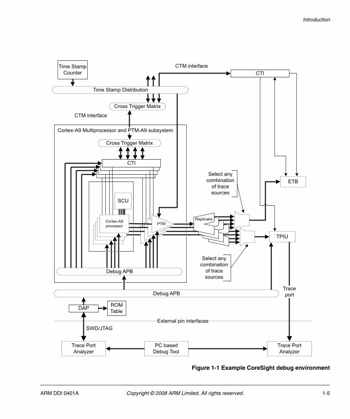
1.1.2 The CoreSight debug environment
The PTM-A9 is designed for use with CoreSight, an extensible, system-wide debug and trace architecture from ARM.
A software debugger provides the user interface to the PTM-A9. You can use this interface to configure the PTM-A9 facilities such as filtering and optional parts of the trace, such as timestamping. The same user interface is used to configure the other CoreSight components such as the Trace Port Interface Unit (TPIU), and to access the processor debug and performance monitor units. The debugger also interprets the trace information that has been output.
In addition, a CoreSight system can provide memory mapped access from the processor to its own debug and trace components.
The PTM-A9 outputs its trace stream to the AMBA 3 ATB interface. The CoreSight infrastructure provides the following options:
• Export the trace information through a trace port. An external Trace Port Analyzer (TPA) captures the trace information as Figure 1-1 on page 1-5 shows.
ARM DDI 0401A Copyright © 2008 ARM Limited. All rights reserved. 1-3

Introduction
• Write the trace information directly to an on-chip Embedded Trace Buffer (ETB). You can read out the trace at low speed using a JTAG or Serial Wire interface when the trace capture is complete as Figure 1-1 on page 1-5 shows.
The debugger extracts the captured trace data from the TPA or ETB and decompresses it to provide full disassembly, with symbols, of the code that was executed. The PTM-A9 provides to the debugger the capability to link this data back to the original high-level source code, to provide a visualization of how the code was executed on the target system.
The PTM-A9-A9 provides a mechanism for inserting a global timestamp in the trace stream that it generates. You can use this as an alternative or in addition to the cycle counting function. Trace tools can use timestamps to correlate trace from several trace sources. In order to use the timestamp function, the system integrator must provide a timestamp count to all trace sources that generate timestamps.
Figure 1-1 on page 1-5 shows how the PTM-A9 fits into the CoreSight debug environment. See the CoreSight Architecture Specification for more information.
In Figure 1-1 on page 1-5, the PTM-A9 and the Cross Trigger Interface (CTI), are part of a CoreSight system consisting of other processors with PTMs, and various other trace sources. You can program the CoreSight components using the Debug Access Port (DAP) through the CoreSight Debug APB bus. The system outputs trace over the ATB trace bus, and either exports it through the Trace Port Interface Unit (TPIU), or stores it in the Embedded Trace Buffer (ETB). Figure 1-1 on page 1-5 shows the trace sources connecting to both a TPIU and the ETB.
1-4 Copyright © 2008 ARM Limited. All rights reserved. ARM DDI 0401A
Introduction
Figure 1-1 Example CoreSight debug environment
Cross Trigger Matrix
TPIU
Traceport
Debug APB
Cross Trigger Matrix
Debug APB
CTI
SCU
Cortex-A9 Multiprocessor and PTM-A9 subsystem
DAP
ETB
Trace Port Analyzer
Trace Port Analyzer
PC based Debug Tool
External pin interfaces
ROM Table
Time Stamp Counter
CTM interfaceCTI
ReplicatorPTMCortex-A9
processor
Time Stamp Distribution
SWD/JTAG
CTM interface
Select any combination
of trace sources
Select any combination
of trace sources
ARM DDI 0401A Copyright © 2008 ARM Limited. All rights reserved. 1-5

Introduction
1.2 Program Trace Macrocell configuration
Table 1-1 shows the options implemented in the PTM-A9.
Table 1-1 PTM-A9 implementation options
Resource Implemented, or number of instances
Number of address comparator pairs 4
Context ID comparators 1
Embedded ICE watchpoint inputs 0
Counters 2
Sequencers 1
External inputs 4
External outputs 2
Extended external inputs, PMUEVENT 29
Extended external input selectors 2
Instrumentation resources 0
FIFOFULL supported No
Software access to registers? Yes
FIFO depth 72 bytes
Trace output ATB bus
1-6 Copyright © 2008 ARM Limited. All rights reserved. ARM DDI 0401A

Introduction
1.3 Program Flow Trace macrocell components
Figure 1-2 shows the main functional blocks of the PTM-A9.
Figure 1-2 Program Flow Trace macrocell functional blocks
1.3.1 Processor input FIFO
This block buffers the output from the processor trace interface until the execution of each waypoint is confirmed by the processor.
ATCLKATCLKEN
ATB
Trace blocks
Main FIFO
PTM-A9 for the Cortex-A9 Processor
CLK
Processor input FIFO
Processorinterface
Synchronization
Trace outSynchronization
CLK domain
ATCLK domain
Level shifters to be added at implementation
DebugAPB APB interface
Filtering and triggering resources
FIFOcontrol
ARM DDI 0401A Copyright © 2008 ARM Limited. All rights reserved. 1-7

Introduction
1.3.2 Trace blocks
These blocks generate the compressed trace based on the waypoint signals provided by the Cortex-A9 processor and the trace control signals from the resource blocks. This trace is passed to the FIFO.
1.3.3 Main FIFO
These blocks provide a buffer for bursts of trace data and manage the transfer of trace data into the ATCLK domain.
1.3.4 Clock domains
The PTM-A9 has its own clock domain, CLK, that must be synchronous with the processor clock. This clock domain is asynchronous to the ATCLK domain.
1.3.5 Level shifters
If you use Intelligent Energy Management (IEM) with the PTM-A9, you can add level shifters during implementation. Level shifters shift the voltage level for the synchronization logic crossing between voltage domains.
1.3.6 Cross-Trigger Interface
The PTM-A9 enables cross-triggering using CTIs connected together through a Cross Trigger Matrix (CTM). Figure 1-3 on page 1-9 and Figure 1-4 on page 1-10 show how each CTI is connected to its corresponding processor and PTM-A9. This connection includes the ability for a debugger to synchronize debug entry and exit between multiple processors.
1-8 Copyright © 2008 ARM Limited. All rights reserved. ARM DDI 0401A

Introduction
Figure 1-3 Cortex-A9 CTI connections
Figure 1-4 on page 1-10 shows the Cortex-A9 connections specific to debug request and restart.
CPU0
CORTEXA9MP
PTM0
PTMDBGRQ
WPT*
EDBGRQ[0]
WPT*0
PTMPWRUPPTMPWRUP[0]
CTI0
PTMDBGACKDBGACK[0]
PTMEXTOUT[1:0]
PTMEXTIN[3:0]
PTMTRIGGERPMUIRQ[0]
COMMTX[0]
CLK
CLKCLK
CTICLK
ATCLK
ATCLK
TRIGIN[3:2]
TRIGOUT[4:1]
TRIGIN[6]
TRIGOUT[0]TRIGOUTACK[0]
TRIGIN[1]
TRIGIN[4]
TRIGIN[0]TRIGINACK[0]
COMMRX[0] TRIGIN[5]
ATB
CTICHIN/CTICHOUT
PMUEVENT[28:0]PMUEVENT0[28:0]
STANDBYWFISTANDBYWFI
TRIGOUT[5]TRIGOUTACK[5]
CTMCTIEXTTRIG0
CTIEXTTRIGACK0
EDBGRQ[0]nCTIRQ[0]
restart logic
DBGRESTART[0]DBGRESTARTED[0]
TRIGOUT[7]TRIGOUTACK[7]
TRIGOUT[6]
nIRQ[0]
nIRQ[0]
STANDBYWFE
ARM DDI 0401A Copyright © 2008 ARM Limited. All rights reserved. 1-9

Introduction
Figure 1-4 Cortex-A9 debug request and restart-specific connections
D QDBGTRIGGERREQ
DBGTRIGGERACK
Processor CLK
CTITRIGIN[0]
CTITRIGINACK[0]
EDBGRQ CTITRIGOUT[0]
CTITRIGOUTACK[0]
DBGRESTARTEDCTITRIGOUTACK[7]
DBGRESTART CTITRIGOUT[7]
CPU0 CTI0
DBGACK
0
1DBGRESTARTACK
D Q
DBGRESTARTREQ
D Q
1-10 Copyright © 2008 ARM Limited. All rights reserved. ARM DDI 0401A

Introduction
1.4 Prohibited regions for trace
The Cortex-A9 processor may prohibit tracing for some regions of code. When the processor is executing code from a prohibited region, the PTM-A9 does not output any information about program execution. The PTM-A9 resumes tracing when the processor leaves the prohibited region, see the Program Flow Trace Architecture Specification.
To decide whether an instruction can be traced, the processor examines:
• the current security level
• the current privilege level
• the state of the SPNIDEN and SPIDEN input pins
• the state of the SUNIDEN control bit set using MCR p15, 0, Rd, c1, c0, 0.
Table 1-2 shows the rules that determine whether trace is prohibited.
Table 1-2 Prohibited region decision table
Security level
Privilege level
NIDEN DBGEN SPNIDEN SPIDEN SUNIDEN Prohibited
x x LOW LOW x x x Yes
Non-secure x HIGH x x x x No
Non-secure x x HIGH x x x No
Secure User HIGH x x x Set No
Secure User x HIGH x x Set No
Secure User HIGH x LOW LOW Clear Yes
Secure User x HIGH LOW LOW Clear Yes
Secure User HIGH x HIGH x Clear No
Secure User x HIGH HIGH x Clear No
Secure User HIGH x x HIGH Clear No
Secure User x HIGH x HIGH Clear No
Secure Privileged HIGH x LOW LOW x Yes
Secure Privileged x HIGH LOW LOW x Yes
Secure Privileged HIGH x HIGH x x No
ARM DDI 0401A Copyright © 2008 ARM Limited. All rights reserved. 1-11

Introduction
This elseif statement combines the decision table elements:
If (~NIDEN and ~DBGEN)Prohibited = 1
else if (Security level == Non-secure)Prohibited = 0
else if ((Privilege level == user) and (SUNIDEN))Prohibited = 0
else if (SPIDEN or SPNIDEN)Prohibited = 0
elseProhibited = 1
Secure Privileged x HIGH HIGH x x No
Secure Privileged HIGH x x HIGH x No
Secure Privileged x HIGH x HIGH x No
Table 1-2 Prohibited region decision table (continued)
Security level
Privilege level
NIDEN DBGEN SPNIDEN SPIDEN SUNIDEN Prohibited
1-12 Copyright © 2008 ARM Limited. All rights reserved. ARM DDI 0401A

Introduction
1.5 Reset behavior
The Main Control Register, 0x00, is reset only on a power-on reset, nPTMRESET LOW. See Chapter 2 Programmer’s Model for a description of the reset values for specific registers.
The resets for the processor and the PTM-A9 are usually separate to allow tracing through a processor reset. If the PTM-A9 is reset, tracing stops until the PTM-A9 is re-programmed and re-enabled. However, if the processor is reset, the last waypoint provided by the processor before the reset might not be traced.
ARM DDI 0401A Copyright © 2008 ARM Limited. All rights reserved. 1-13

Introduction
1.6 Product revisions
This manual is for revision r0p0 of the CoreSight Program Trace Macrocell for the Cortex-A9 processor (PTM-A9). See Product revision status on page x for details of revision numbering.
1-14 Copyright © 2008 ARM Limited. All rights reserved. ARM DDI 0401A

Chapter 2 Programmer’s Model
This chapter describes the implementation-specific characteristics of the PTM-A9. It contains the following sections:
• Programming the PTM-A9 on page 2-2
• Register short names on page 2-5
• PTM-A9 register summary on page 2-6
• Implementation-defined behavior on page 2-34
• Turning off the PTM-A9 on page 2-35
• Interaction with the performance monitoring unit on page 2-36.
ARM DDI 0401A Copyright © 2008 ARM Limited. All rights reserved. 2-1

Programmer’s Model
2.1 Programming the PTM-A9
When the PTM-A9 is powered on or reset, you must program all PTM registers before you enable tracing. If you do not do so, the trace results are Unpredictable.
When programming the PTM-A9 registers you must enable all the changes at the same time. For example, if the counter is reprogrammed before the trigger condition has been correctly set up, it might start to count based on incorrect events.
You access the registers of the PTM-A9 through the CoreSight Debug APB bus. The PTM-A9 implements the CoreSight lock access mechanism, and can distinguish between memory-mapped accesses from on-chip software and memory-mapped accesses from a debugger, for example by using the CoreSight Debug Access Port (DAP).
See the CoreSight Program Flow Trace Architecture Specification for more information about programming the PTM-A9.
2.1.1 Using the Programming bit
Use the Programming bit in the Main Control Register (see Main Control Register, ETMCR on page 2-9) to disable all operations during programming.
When the Programming bit is set to 0 you must not write to registers other than the Main Control Register, because this can lead to Unpredictable behavior.
When setting the Programming bit, you must not change any other bits of the Main Control Register. You must only change the value of bits other than the Programming bit of the Control Register when bit [1] of the Status Register is set to 1. ARM recommends that you use a read-modify-write procedure when changing the Main Control Register.
When the Programming bit is set to 1:
• The FIFO is allowed to empty and then no more trace is produced.
• The counters, sequencer, and start/stop block are held in their current state.
• The external outputs are forced LOW.
Figure 2-1 on page 2-3 shows a flow diagram of the procedure to program the PTM-A9 registers.
2-2 Copyright © 2008 ARM Limited. All rights reserved. ARM DDI 0401A

Programmer’s Model
Figure 2-1 Programming the PTM-A9 registers
2.1.2 Programming registers
A reset of the PTM-A9 initializes the following registers:
• Main Control Register, ETMCR on page 2-9
• Synchronization Frequency Register, ETMSYNCFR on page 2-17
• CoreSight Trace ID Register, ETMTRACEIDR on page 2-22
• the CoreSight registers at offsets 0xF00 through 0xFFC
• Peripheral Identification registers on page 2-31
Start
Set Programming bitin Main Control Register
Yes
No
Read Status Register
Is bit 1 ofStatus Register (Progbit) set?
Program all registers
Clear Programming bit in Main Control Register
Read Status Register
End
Yes
No
Is bit 1 ofStatus Register (Progbit) set?
ARM DDI 0401A Copyright © 2008 ARM Limited. All rights reserved. 2-3
Programmer’s Model
• Component Identification registers on page 2-32.
To start tracing, you must program the following registers to avoid Unpredictable behavior:
• Main Control Register, ETMCR on page 2-9
• Trigger Event Register, TTER
• TraceEnable Control registers on page 2-13
• CoreSight Trace ID Register, ETMTRACEIDR on page 2-22.
You might also need to program the following:
• Address Comparator registers on page 2-16 if the respective address comparators are used
• Counter registers on page 2-17 if the respective counters are used
• Sequencer registers if the sequencer is used
• External Output Event Registers if the external outputs are used
• Context ID comparator registers if the context ID comparator is used
• Extended External Input Selection Register, ETMEXTINSELR on page 2-20 if the extended external inputs are used.
2-4 Copyright © 2008 ARM Limited. All rights reserved. ARM DDI 0401A

Programmer’s Model
2.2 Register short names
All of the PTM-A9 registers have short names. Most of these are mnemonics for the full name of the register, except that the short name starts with the letters ETM, indicating that the register is defined by an ARM trace architecture. The ETM architecture is the original ARM trace architecture, and because register assignments are consistent across the trace architectures the register short names always take the ETM prefix. Table 2-1 gives some examples of the register short names.
The use of the ETM prefix for the register short names means that the short names are distinct from the short names used for other registers, such as the processor control coprocessor registers and the debug registers.
Table 2-1 Examples of register short names
PTM-A9 register name Register short name Explanation of short name
Main Control Register ETMCR Trace Control Register
Trigger Event Register ETMTRIGGER Trace Trigger (Register)
Address Comparator Value Register 3 ETMACVR3 Trace Address Comparator Value Register 3
ARM DDI 0401A Copyright © 2008 ARM Limited. All rights reserved. 2-5
Programmer’s Model
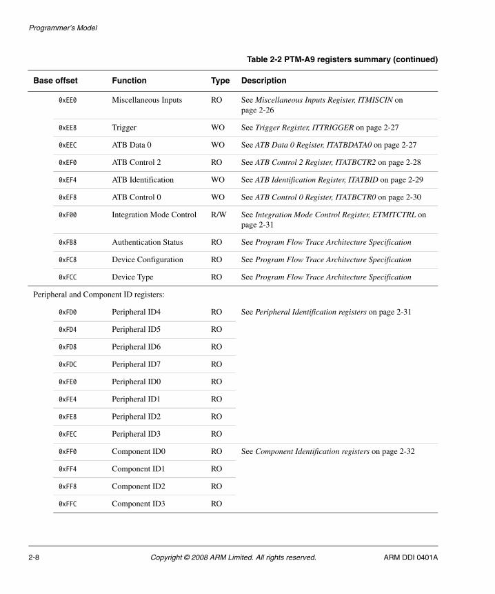
2.3 PTM-A9 register summary
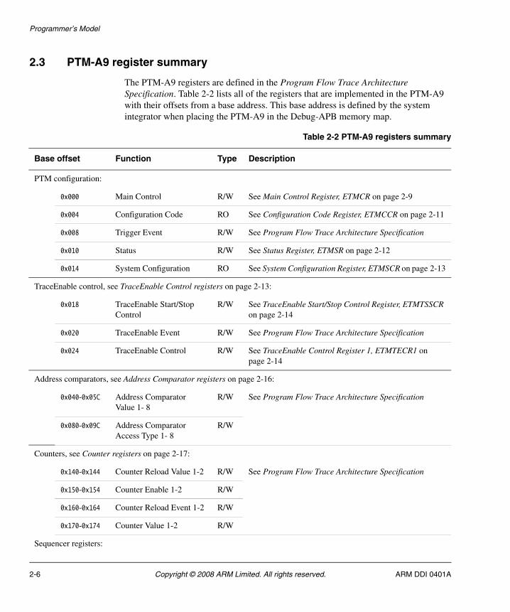
The PTM-A9 registers are defined in the Program Flow Trace Architecture Specification. Table 2-2 lists all of the registers that are implemented in the PTM-A9 with their offsets from a base address. This base address is defined by the system integrator when placing the PTM-A9 in the Debug-APB memory map.
Table 2-2 PTM-A9 registers summary
Base offset Function Type Description
PTM configuration:
0x000 Main Control R/W See Main Control Register, ETMCR on page 2-9
0x004 Configuration Code RO See Configuration Code Register, ETMCCR on page 2-11
0x008 Trigger Event R/W See Program Flow Trace Architecture Specification
0x010 Status R/W See Status Register, ETMSR on page 2-12
0x014 System Configuration RO See System Configuration Register, ETMSCR on page 2-13
TraceEnable control, see TraceEnable Control registers on page 2-13:
0x018 TraceEnable Start/Stop Control
R/W See TraceEnable Start/Stop Control Register, ETMTSSCR on page 2-14
0x020 TraceEnable Event R/W See Program Flow Trace Architecture Specification
0x024 TraceEnable Control R/W See TraceEnable Control Register 1, ETMTECR1 on page 2-14
Address comparators, see Address Comparator registers on page 2-16:
0x040-0x05C Address Comparator Value 1- 8
R/W See Program Flow Trace Architecture Specification
0x080-0x09C Address Comparator Access Type 1- 8
R/W
Counters, see Counter registers on page 2-17:
0x140-0x144 Counter Reload Value 1-2 R/W See Program Flow Trace Architecture Specification
0x150-0x154 Counter Enable 1-2 R/W
0x160-0x164 Counter Reload Event 1-2 R/W
0x170-0x174 Counter Value 1-2 R/W
Sequencer registers:
2-6 Copyright © 2008 ARM Limited. All rights reserved. ARM DDI 0401A

Programmer’s Model
0x180-0x194 Sequencer State Transition Event 1-6
R/W See Program Flow Trace Architecture Specification
0x19C Current Sequencer State R/W See Program Flow Trace Architecture Specification
External output event:
0x1A0-0x1A4 External Output Event 1-2 R/W See Program Flow Trace Architecture Specification
Context ID comparators:
0x1B0 Context ID Comparator Value 1
R/W See Program Flow Trace Architecture Specification
0x1BC Context ID Comparator Mask
R/W See Program Flow Trace Architecture Specification
General control:
0x1E0 Synchronization Frequency
R/W See Synchronization Frequency Register, ETMSYNCFR on page 2-17
0x1E4 ID RO See ID Register, ETMIDR on page 2-17
0x1E8 Configuration Code Extension
RO See Configuration Code Extension Register, ETMCCER on page 2-18
0x1EC Extended External Input Selection
R/W See Extended External Input Selection Register, ETMEXTINSELR on page 2-20
0x1F8 Timestamp Event R/W See Program Flow Trace Architecture Specification
0x1FC Auxiliary Control Register R/W See Auxiliary Control Register, ETMAUXCR on page 2-20
0x200 CoreSight Trace ID R/W See CoreSight Trace ID Register, ETMTRACEIDR on page 2-22
0x304 OS Lock Status RO See OS Lock Status Register, OSLSR on page 2-22
0x314 Device Power-Down Status
RO See Device Power-Down Status Register, ETMPDSR on page 2-22
Integration registers, see Integration registers on page 2-23:
0xEDC Miscellaneous Outputs WO See Miscellaneous Outputs Register, ITMISCOUT on page 2-25
Table 2-2 PTM-A9 registers summary (continued)
Base offset Function Type Description
ARM DDI 0401A Copyright © 2008 ARM Limited. All rights reserved. 2-7
Programmer’s Model
0xEE0 Miscellaneous Inputs RO See Miscellaneous Inputs Register, ITMISCIN on page 2-26
0xEE8 Trigger WO See Trigger Register, ITTRIGGER on page 2-27
0xEEC ATB Data 0 WO See ATB Data 0 Register, ITATBDATA0 on page 2-27
0xEF0 ATB Control 2 RO See ATB Control 2 Register, ITATBCTR2 on page 2-28
0xEF4 ATB Identification WO See ATB Identification Register, ITATBID on page 2-29
0xEF8 ATB Control 0 WO See ATB Control 0 Register, ITATBCTR0 on page 2-30
0xF00 Integration Mode Control R/W See Integration Mode Control Register, ETMITCTRL on page 2-31
0xFB8 Authentication Status RO See Program Flow Trace Architecture Specification
0xFC8 Device Configuration RO See Program Flow Trace Architecture Specification
0xFCC Device Type RO See Program Flow Trace Architecture Specification
Peripheral and Component ID registers:
0xFD0 Peripheral ID4 RO See Peripheral Identification registers on page 2-31
0xFD4 Peripheral ID5 RO
0xFD8 Peripheral ID6 RO
0xFDC Peripheral ID7 RO
0xFE0 Peripheral ID0 RO
0xFE4 Peripheral ID1 RO
0xFE8 Peripheral ID2 RO
0xFEC Peripheral ID3 RO
0xFF0 Component ID0 RO See Component Identification registers on page 2-32
0xFF4 Component ID1 RO
0xFF8 Component ID2 RO
0xFFC Component ID3 RO
Table 2-2 PTM-A9 registers summary (continued)
Base offset Function Type Description
2-8 Copyright © 2008 ARM Limited. All rights reserved. ARM DDI 0401A

Programmer’s Model
For more information about these registers and the packets implemented by the PTM-A9, see the Program Flow Trace Architecture Specification.
2.3.1 Main Control Register, ETMCR
The Main Control Register, ETMCR, controls general operation of the PTM-A9, such as whether tracing is enabled. It is:
• register 0x000, at offset 0x000
• a read/write register.
Figure 2-2 shows the bit assignments for the Main Control Register.
Figure 2-2 Main Control Register bit assignments
Table 2-3 shows the bit assignments for the Main Control Register.
31 28 27 25 24 23 16 15 13 12 8 7 0
Processorselect
Reserved Reserved
Instrumentationresource control
ContextIDsize ReservedCycleAccurateReservedProgBitDebug request controlBranchBroadcastStall processor
PowerDown
19 614 11 1030 29
ReservedReturn stack
enableTimestamp
enable
Table 2-3 Main Control Register bit assignment
Bit Function Description
[31:30] Reserved SBZP
[29] Return stack enable b0 = disabled
b1 = enabled
On reset, this bit is set to b0, disabled
[28] Timestamp enable b0 = disabled
b1 = enabled
On reset, this bit is set to b0, disabled
ARM DDI 0401A Copyright © 2008 ARM Limited. All rights reserved. 2-9

Programmer’s Model
[27:25] Processor select Select for external multiplexor if PTM-A9 is shared between multiple processors. See Program Flow Trace Architecture Specification.
[24] Instrumentation Resource Control RAZ, not implemented.
[23:16] Reserved SBZP
[15:14] ContextIDSize b00 = no context ID tracing
b01 = context ID bits [7:0] traced
b10 = context ID bits [15:0] traced
b11 = context ID bits [31:0] traced.
On reset, this bit is set to b00, no context ID tracing
[13] Reserved SBZP
[12] CycleAccurate b0 = cycle counting disabled
b1 = cycle counting enabled
On reset this bit is set to b0, no cycle counting.
[11] Reserved SBZP
[10] Programming Bit This bit must be set to b1 when the PTM-A9 is being programmed, see Programming the PTM-A9 on page 2-2.
On a PTM reset this bit is set to b1.
[9] Debug request control When set to b1 and the trigger event occurs, the PTMDBGRQ output is asserted until PTMDBGACK is observed. This enables a debugger to force the processor into Debug state.
On PTM reset this bit is set to b0.
[8] Branch Output When this bit is set to b1, addresses are output for all executed branches, both direct and indirect.
On PTM reset this bit is set to b0.
Table 2-3 Main Control Register bit assignment (continued)
Bit Function Description
2-10 Copyright © 2008 ARM Limited. All rights reserved. ARM DDI 0401A

Programmer’s Model
2.3.2 Configuration Code Register, ETMCCR
The Configuration Code Register, ETMCCR, provides information about the configuration of the PTM-A9. It is:
• register 0x001, at offset 0x004
• a 32-bit read-only register.
Figure 2-3 shows the bit assignments for the Configuration Code Register.
Figure 2-3 Configuration Code Register bit assignments
[7] Stall Processor RAZ - Not Implemented
[6:1] Reserved SBZP
[0] PowerDown This bit enables external control of the PTM-A9. This bit must be cleared by the trace software tools at the beginning of a debug session.
When this bit is set to b0, both the PTM-A9 and the trace interface in the processor are enabled.
To avoid corruption of trace data, this bit must not be set before the Programming Status bit in the PTM-A9 Status Register has been read as 1.
On PTM reset this bit is set to b1.
Table 2-3 Main Control Register bit assignment (continued)
Bit Function Description
Reserved Number of external outputs
FIFOFULL logic
Software access support
Trace stop/start block present
Number of Context ID comparators
Number of external inputs
Sequencer
ID Register present
01
31 30 28 27 26 25 24 23 22 20 19 17 16 15 13 12 8 7 4 3 0
0 0 0 1 1 0 1 0 0 1 0 1 0 0 1 0 1 0 Reserved 0 1 0
Number of counters Number of
pairs of address
comparators
ARM DDI 0401A Copyright © 2008 ARM Limited. All rights reserved. 2-11

Programmer’s Model
Table 2-4 shows the bit assignments for the Configuration Code Register. The Configuration Code Register has the value 0x8D294004.
2.3.3 Status Register, ETMSR
The Status Register, ETMSR, provides information about the current status of the trace and trigger logic. It is:
• register 0x004, at offset 0x010
• a read/write register.
Bit [1] of this register shows the effective state of the Programming bit. You must wait for this bit to go to b1 before starting to program the PTM-A9.
This register is described in the CoreSight Program Trace Flow Architecture Specification.
Table 2-4 Configuration Code Register bit assignments
Bits Field Function
[31] ID Register present Indicates that the ID Register is present. See ID Register, ETMIDR on page 2-17.
[30:28] - Reserved, RAZ on reads.
[27] Software access Indicates that software access is supported, see Programming the PTM-A9 on page 2-2.
[26] Trace stop/start block Indicates that the trace start/stop block is present.
[25:24] Number of Context ID comparators Specifies the number of Context ID comparators, one.
[23] FIFOFULL logic Indicates that it is not possible to stall the processor to prevent FIFO overflow.
[22:20] Number of external outputs Specifies the number of external outputs, two.
[19:17] Number of external inputs Specifies the number of external inputs, four.
[16] Sequencer Indicates that the sequencer is present.
[15:13] Number of counters Specifies the number of counters, two.
[12:4] - Reserved
[3:0] Number of pairs of address comparators Specifies the number of address comparator pairs, four.
2-12 Copyright © 2008 ARM Limited. All rights reserved. ARM DDI 0401A

Programmer’s Model
2.3.4 System Configuration Register, ETMSCR
The System Configuration Register, ETMSCR, shows the features supported by the ASIC. Some of the contents of this register are based on inputs provided by the ASIC. It is:
• register 0x005, at offset 0x014
• a read-only register.
Figure 2-4 shows the bit assignments for the System Configuration Register.
Figure 2-4 System Configuration Register bit assignments
Table 2-5 shows the bit assignments for the System Configuration Register.
2.3.5 TraceEnable Control registers
The CoreSight Program Flow Trace Architecture Specification describes the TraceEnable mechanism that controls when trace is generated. Three registers control and configure the operation of TraceEnable. They are described in the following sections:
• TraceEnable Start/Stop Control Register, ETMTSSCR on page 2-14
(N -1), where N = number of processors supported by PTMReserved
FIFOFULL supported
31 15 12 8 7 0
Reserved Reserved
14 11 9
Table 2-5 System Configuration Register bit assignments
Bit Description
[31:15] Reserved, SBZP.
[14:12] Number of supported processors minus 1.
The value of this field is set by the MAXCORES[2:0] input to the PTM-A9, see Program Flow Trace Architecture Specification.
[11:9] Reserved, SBZP.
[8] Read Only, as b0 - FIFOFULL is not supported.
[7:0] Reserved, SBZP.
ARM DDI 0401A Copyright © 2008 ARM Limited. All rights reserved. 2-13

Programmer’s Model
• TraceEnable Event Register, See Program Flow Trace Architecture Specification
• TraceEnable Control Register 1, ETMTECR1.
2.3.6 TraceEnable Start/Stop Control Register, ETMTSSCR
The TraceEnable Start/Stop Control RegisteR, ETMTSSCR, specifies the single address comparators that hold the trace start and stop addresses that control the TraceEnable Start/Stop block. It is:
• register 0x006, at offset 0x018
• a read/write register.
Figure 2-5 shows bit assignments for the TraceEnable Start/Stop Control Register.
Figure 2-5 TraceEnable Start/Stop Control Register bit assignments
Table 2-6 shows the bit assignments for the TraceEnable Start/Stop Control Register.
2.3.7 TraceEnable Control Register 1, ETMTECR1
The TraceEnable Control Register, ETMTECR1:
• enables the start/stop logic
• specifies the address range comparators used for include or exclude control
• defines whether the specified address range comparators are used for include or exclude control.
Reserved
31 16 15 0
Reserved
8 7 6 5 4 3 2 1 8 7 6 5 4 3 2 1
Stop addresses Start addresses
23 724 8
Table 2-6 TraceEnable Start/Stop Control Register bit assignments
Bit Description
[31:24] Reserved
[23:16] When a bit is set to 1, it selects a single address comparator (8-1) as a stop address for the TraceEnable Start/Stop block. For example, if you set bit [16] to 1 it selects single address comparator 1 as a stop address.
[15:8] Reserved
[7:0] When a bit is set to 1, it selects a single address comparator (8-1) as a start address for the TraceEnable Start/Stop block. For example, if you set bit [0] to 1 it selects single address comparator 1 as a start address.
2-14 Copyright © 2008 ARM Limited. All rights reserved. ARM DDI 0401A

Programmer’s Model
It is:
• register 0x009, at offset 0x024
• a read/write register.
Figure 2-6 shows the bit assignments for the TraceEnable Control Register.
Figure 2-6 TraceEnable Control Register bit assignments
Table 2-7 shows the bit assignments for the TraceEnable Control Register.
Tracing all instructions
To trace all processor execution:
• set bit [24], the exclude/include flag, in this register to 1
• set all other bits in this register to 0
Reserved
31 0
Reserved
Address comparators
26 25 24 23 4 3
4 3 2 1Exclude/include flag
Trace control enable
Table 2-7 TraceEnable Control Register bit assignments
Bit Description
[31:26] Reserved, SBZP.
[25] Trace start/stop control enable. The possible values of this bit are:
0 Tracing is unaffected by the trace start/stop logic.
1 Tracing is controlled by the trace on and off addresses configured for the trace start/stop logic.
The trace start/stop resource, see Table 2-26 on page 2-33, is not affected by the value of this bit.
[24] Exclude/include flag. The possible values of this bit are:
0 Include. The specified address range comparators indicate the regions where tracing can occur. No tracing occurs outside this region.
1 Exclude. The specified address range comparators indicate regions to be excluded from the trace. When outside an exclude region, tracing can occur.
[23:4] Reserved, SBZP.
[3:0] When a bit is set to 1, it selects an address range comparator, 4-1, for include/exclude control. For example, bit [0] set to 1 selects address range comparator 1.
ARM DDI 0401A Copyright © 2008 ARM Limited. All rights reserved. 2-15

Programmer’s Model
• set register 0x008, the TraceEnable Event register, to 0x0000006F (TRUE).
This has the effect of excluding nothing, that is, tracing everything, and setting the trace enable event to always true, with the start/stop logic ignored.
2.3.8 Address Comparator registers
The PTM-A9 implements eight pairs of Address Comparator registers. Table 2-8 shows the organization of these registers.
The CoreSight Program Trace Flow Architecture Specification describes the operation of these registers in the PTM-A9.
Table 2-8 PTM-A9 Address Comparator Registers
Address Comparator
Address Comparator Value Register Address Comparator Access Type Register
1 ETMACVR1, register 0x010, at offset 0x040 ETMACTR1, register 0x020, at offset 0x080
2 ETMACVR2, register 0x011, at offset 0x044 ETMACTR2, register 0x021, at offset 0x084
3 ETMACVR3, register 0x012, at offset 0x048 ETMACTR3, register 0x022, at offset 0x088
4 ETMACVR4, register 0x013, at offset 0x04C ETMACTR4, register 0x023, at offset 0x08C
5 ETMACVR5, register 0x014, at offset 0x050 ETMACTR5, register 0x024, at offset 0x090
6 ETMACVR6, register 0x015, at offset 0x054 ETMACTR6, register 0x025, at offset 0x094
7 ETMACVR7, register 0x016, at offset 0x058 ETMACTR7, register 0x026, at offset 0x098
8 ETMACVR8, register 0x017, at offset 0x05C ETMACTR8, register 0x027, at offset 0x09C
2-16 Copyright © 2008 ARM Limited. All rights reserved. ARM DDI 0401A
Programmer’s Model
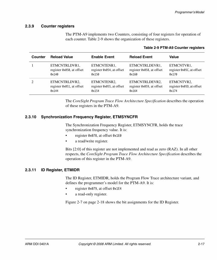
2.3.9 Counter registers
The PTM-A9 implements two Counters, consisting of four registers for operation of each counter. Table 2-9 shows the organization of these registers.
The CoreSight Program Trace Flow Architecture Specification describes the operation of these registers in the PTM-A9.
2.3.10 Synchronization Frequency Register, ETMSYNCFR
The Synchronization Frequency Register, ETMSYNCFR, holds the trace synchronization frequency value. It is:
• register 0x078, at offset 0x1E0
• a read/write register.
Bits [2:0] of this register are not implemented and read as zero (RAZ). In all other respects, the CoreSight Program Trace Flow Architecture Specification describes the operation of this register in the PTM-A9.
2.3.11 ID Register, ETMIDR
The ID Register, ETMIDR, holds the Program Flow Trace architecture variant, and defines the programmer’s model for the PTM-A9. It is:
• register 0x079, at offset 0x1E4
• a read-only register.
Figure 2-7 on page 2-18 shows the bit assignments for the ID Register.
Table 2-9 PTM-A9 Counter registers
Counter Reload Value Enable Event Reload Event Value
1 ETMCNTRLDVR1, register 0x050, at offset 0x140
ETMCNTENR1, register 0x054, at offset 0x150
ETMCNTRLDEVR1, register 0x058, at offset 0x160
ETMCNTVR1, register 0x05C, at offset 0x170
2 ETMCNTRLDVR2, register 0x051, at offset 0x144
ETMCNTENR2, register 0x055, at offset 0x154
ETMCNTRLDEVR2, register 0x059, at offset 0x164
ETMCNTVR2, register 0x05D, at offset 0x174
ARM DDI 0401A Copyright © 2008 ARM Limited. All rights reserved. 2-17

Programmer’s Model
Figure 2-7 ID Register bit assignments
Table 2-10 shows the bit assignments for the ID Register. The values of the fields in this register are consistent with the ETM architecture, see Embedded Trace Macrocell Architecture Specification.
2.3.12 Configuration Code Extension Register, ETMCCER
The Configuration Code Extension Register, ETMCCER, provides additional information about the configuration of the PTM-A9. It is:
• register 0x7A, at offset 0x1E8
• a read-only register
00000 0 1 1 0 0 0 01 1 1 10 1 0 0 0 0 0 1 1 1 1
Security Extensions supported
31 17 16 15 12 8 7 4 3 018 11
Architecture version number
24 23 20 19
Major Minor
Implementation revision
Reserved
21
Reserved32-bit Thumb instructions supported
Reserved
ReservedImplementer code
Table 2-10 ID Register bit assignments
Bit Description
[31:24] Implementor code. This field reads as 0x41, ASCII code for A, indicating ARM Limited.
[23:21] Reserved, RAZ.
[20] Reserved. This bit is RAO.
[19] Support for Security Extensions. The value of this bit is 1, indicating that the processor implements the ARM architecture Security Extensions.
[18] Support for 32-bit Thumb instructions. The value of this bit is 1, indicating that a 32-bit Thumb instruction is traced as a single instruction.
[17:16] Reserved, RAZ.
[15:12] Reserved. This field reads as b1111.
[11:8] b0011 - Major architecture version number.
[7:4] b0000 - Minor architecture version number.
[3:0] Implementation revision.
2-18 Copyright © 2008 ARM Limited. All rights reserved. ARM DDI 0401A

Programmer’s Model
Figure 2-8 shows the bit assignments for the Configuration Code Extension Register.
Figure 2-8 Configuration Code Extension Register format
Table 2-11 shows the bit assignments for the Configuration Code Extension Register.
0111 10 0 0 0
31 24 23 22 21 16 15 13 12 11 10 3 2 0
1 1 0 0 0 1 1 0 1
Return stack implemented
Reserved Reserved
Number of instrumentation
resources
Reserved Register reads
Extended external input bus size
Number of extended external input selectors Timestamping implemented
2526
SMB/SDB treated as waypoint
Timestamps for SMB/DSB
0 0
Table 2-11 Configuration Code Extension Register bit functions
Bits Function
[31:26] Reserved, RAZ on reads.
[25] b0 - Timestamps not generated for DMB/DSB.
[24] b0 - DMB/DSB instructions are not treated as waypoints.
[23] b1 - Return stack implemented.
[22] b1 - Timestamping implemented.
[21:16] Reserved, RAZ on reads.
[15:13] b000 - Specifies the number of instrumentation resources.
[12] Reserved, RAO.
[11] b1 - Indicates that all registers, except some Integration Test Registers, are readable.
See Using the Integration Test Registers on page 2-23 for details of the access permission to the Integration Test Registers. Registers with names that start with IT are the Integration Test Registers, for example ITATBCTR1.
[10:3] b00011101 - Specifies the size of the extended external input bus, 29.
[2:0] b010 - Specifies the number of extended external input selectors, 2.
ARM DDI 0401A Copyright © 2008 ARM Limited. All rights reserved. 2-19

Programmer’s Model
2.3.13 Extended External Input Selection Register, ETMEXTINSELR
The Extended External Input Selection Register, ETMEXTINSELR, selects inputs from the PMUEVENT bus to use as PTM resources. It is
• register 0x07B, at offset 0x1EC
• a read/write register.
Figure 2-9 shows the bit assignments for this register.
Figure 2-9 Extended External Input Selection Register bit assignment
Table 2-12 shows the bit assignment for the Extended External Input Selection Register.
2.3.14 Auxiliary Control Register, ETMAUXCR
The Auxiliary Control Register, ETMAUXCR, provides additional controls It is:
• register 0x07F, at offset 01FC
• a read/write register.
Figure 2-10 shows the bit assignments for this register.
Figure 2-10 Auxiliary Control Register bit assignments
Reserved
31 16 15 8 7 0
Second extended external input selector
First extended external input selector
Table 2-12 Extended External Input Register bit functions
Bits Function
[31:16] Reserved
[15:8] Second Extended External Input Selector
[7:0] First Extended External Input Selector
31 4 3 2 1 0
Reserved
Disable forced overflowDisable timestamps on barriers
Disable waypoint update packetForce synchronization packet insertion
2-20 Copyright © 2008 ARM Limited. All rights reserved. ARM DDI 0401A

Programmer’s Model
Table 2-13 shows the bit assignments for the Auxiliary Control Register
When setting any of bits [2:0] of this register the PTM-A9 behavior might contradict the Program Flow Trace Architecture Specification. Tools must be aware of the implications of setting any of these bits:
• Bit [0] might be set if the FIFO overflows due to the forced overflow condition. See the Program Flow Trace Architecture Specification for details on this condition. If this bit is set, tools must be aware that synchronization might not occur within the desired synchronization period.
Table 2-13 Auxiliary Control Register bit assignments
Bits Function Description
[31:4] - Reserved
[3] Force synchronization packet insertion
Force insertion of synchronization packets, regardless of current trace activity. Possible values for this bit are:
b0 = Synchronization packets delayed when trace activity is high. This is the reset value.
b1 = Synchronization packets inserted regardless of trace activity.
This bit might be set if synchronization packets occur too far apart. Setting this bit might cause the trace FIFO to overflow more frequently when trace activity is high.
[2] Disable waypoint update packet
Specifies whether the PTM-A9 issues waypoint update packets if there are more than 4096 bytes between waypoints. Possible values for this bit are:
b0 = PTM always issues update packets if there are more than 4096 bytes between waypoints. This is the reset value.
b1 = PTM does not issue waypoint update packets unless required to do so as the result of an exception or debug entry.
[1] Disable timestamps on barriers
Specifies whether the PTM-A9 issues a timestamp on a barrier instruction. Possible values for this bit are:
b0 = PTM issues timestamps on barrier instructions. This is the reset value.
b1 = PTM does not issue timestamps on barriers
[0] Disable forced overflow Specifies whether the PTM-A9 enters overflow state when synchronization is requested, and the previous synchronization sequence has not yet completed. This does not affect entry to overflow state when the FIFO becomes full. Possible values for this bit are:
b0 = Forced overflow enabled. This is the reset value.
b1 = Forced overflow disabled.
ARM DDI 0401A Copyright © 2008 ARM Limited. All rights reserved. 2-21

Programmer’s Model
• Bit [1] might be set if timestamp packets are not required on barrier instructions. Typically, this might be set when using timestamping as a low-bandwidth measure of time, but might make correlation of multiple trace sources impossible.
• Bit [2] might be set if tools do not require the waypoint update packet that is output if there are more than 4096 bytes between waypoints.
2.3.15 CoreSight Trace ID Register, ETMTRACEIDR
The CoreSight Trace ID Register, ETMTRACEIDR, defines a 7-bit Trace ID for output to the trace bus. The register is:
• register 0x080, at offset 0x200
• a read/write register.
Before trace is generated, you must program this register with a non-reserved value. Reserved values are 0x00 and any value in the range 0x70-0x7F. The reset value of this register is 0x00.
The CoreSight Program Trace Flow Architecture Specification describes the operation of this register in the PTM-A9.
2.3.16 Device Power-Down Status Register, ETMPDSR
The Device Power-Down Status Register, ETMPDSR, indicates the power-down status of the PTM-A9. It is:
• register 0xC5, at offset 0x314
• a read-only register.
This register always reads as 0x00000001, indicating that the PTM-A9 Trace Registers can be accessed.
2.3.17 OS Lock Status Register, OSLSR
The OS Lock Status Register, OSLSR, shows whether trace register locking is implemented for the PTM-A9 macrocell. It is:
• register 0x0C1, at offset 0x304 in a memory-mapped implementation
• a read-only register.
For the PTM-A9, the OS Lock Status Register Reads As Zero (RAZ) to show that OS Locking is not implemented.
2-22 Copyright © 2008 ARM Limited. All rights reserved. ARM DDI 0401A

Programmer’s Model
2.3.18 Integration registers
A CoreSight PTM can provide registers that let you test your integration of the PTM into your design. This section describes the integration registers that are implemented for the PTM-A9. It contains the following sections:
• Using the Integration Test Registers
• Miscellaneous Outputs Register, ITMISCOUT on page 2-25
• Miscellaneous Inputs Register, ITMISCIN on page 2-26
• Trigger Register, ITTRIGGER on page 2-27
• ATB Data 0 Register, ITATBDATA0 on page 2-27
• ATB Control 2 Register, ITATBCTR2 on page 2-28
• ATB Identification Register, ITATBID on page 2-29
• ATB Control 0 Register, ITATBCTR0 on page 2-30
Using the Integration Test Registers
Table 2-14 lists the Integration Test Registers implemented by the PTM-A9.
To access these registers you must first set bit [0] of the Integration Mode Control Register to 1. See Integration Mode Control Register, ETMITCTRL on page 2-31. When this bit is set:
• You can use the write-only Integration Test Registers to set the outputs of some of the PTM-A9 signals. Table 2-15 on page 2-24 lists the signals that you can control in this way.
Table 2-14 Integration Test Registers
Base offset Function Type Description
0xEDC Miscellaneous Outputs WO See Miscellaneous Outputs Register, ITMISCOUT on page 2-25
0xEE0 Miscellaneous Inputs RO See Miscellaneous Inputs Register, ITMISCIN on page 2-26
0xEE8 Trigger WO See Trigger Register, ITTRIGGER on page 2-27
0xEEC ATB Data WO See ATB Data 0 Register, ITATBDATA0 on page 2-27
0xEF0 ATB Control 2 RO See ATB Control 2 Register, ITATBCTR2 on page 2-28
0xEF4 ATB Identification WO See ATB Identification Register, ITATBID on page 2-29
0xEF8 ATB Control 0 WO See ATB Control 0 Register, ITATBCTR0 on page 2-30
ARM DDI 0401A Copyright © 2008 ARM Limited. All rights reserved. 2-23

Programmer’s Model
• You can use the read-only Integration Test Registers to read the state of some of the PTM-A9 input signals. Table 2-16 lists the signals that you can read in this way.
See the Program Flow Trace Architecture Specification for more information.
Table 2-15 Output signals that can be controlled by the Integration Test Registers
Register Signal Bit Description
ITMISCOUT PTMEXTOUT[1:0] [9:8] See Miscellaneous Outputs Register, ITMISCOUT on page 2-25
PTMIDLEnACK [5]
PTMDBGREQ [4]
ITATBDATA0 ATDATAM[31] [4] See ATB Data 0 Register, ITATBDATA0 on page 2-27
ATDATAM[23] [3]
ATDATAM[15] [2]
ATDATAM[7] [1]
ATDATAM[0] [0]
ITTRIGGER PTMTRIGGER [0] See Trigger Register, ITTRIGGER on page 2-27
ITATBID ATIDM[6:0] [6:0] See ATB Identification Register, ITATBID on page 2-29
ITATBCTR0 ATBYTESM[9:8] [9:8] See ATB Control 0 Register, ITATBCTR0 on page 2-30
AFREADYM [1]
ATVALIDM [0]
Table 2-16 Input signals that can be read by the Integration Test Registers
Register Signal Bit Description
ITMISCIN STANDBYWFI [6] See Miscellaneous Inputs Register, ITMISCIN on page 2-26
PTMDBGACK [4]
PTMEXTIN[3:0] [3:0]
ITATBCTR2 AFVALIDM [1] ATB Control 2 Register, ITATBCTR2 on page 2-28
ATREADYM [0]
2-24 Copyright © 2008 ARM Limited. All rights reserved. ARM DDI 0401A

Programmer’s Model
The CoreSight Components Technical Reference Manual gives a full description of the use of the Integration Test Registers to check integration. In brief:
• When bit [0] of the Integration Mode Control Register is set, values written to the write-only Integration Test Registers map onto the specified outputs of the PTM-A9. For example, writing 0x3 to ITMISCOUT[9:8] causes EXTOUT[1:0] to take the value 0x3.
• When bit [0] of the Integration Mode Control Register is set, values read from the read-only integration test registers correspond to the values of the specified inputs of the PTM-A9. For example, if you read ITMISCIN[3:0] you obtain the value of PTMEXTIN.
Miscellaneous Outputs Register, ITMISCOUT
The Miscellaneous Outputs Register, ITMISCOUT, controls signal outputs when bit [0] of the Integration Mode Control Register is set. It is:
• register 0x3B7, at offset 0xEDC
• a write-only register.
Figure 2-11 shows the bit arrangement of the ITMISCOUT Register.
Figure 2-11 ITMISCOUT Register format
Table 2-17 shows how the bit values correspond with the ITMISCOUT Register functions.
5
Reserved
31 0
PTMIDLEnACK
6
PTMEXTOUT[1:0]
3489 710
Reserved
Reserved
PTMDBGREQ
Table 2-17 ITMISCOUT Register bit functions
Bits Function
[31:10] Reserved, Should Be Zero (SBZ) on writes
[9:8] Drives the PTMEXTOUT[1:0] outputs
[7:6} Reserved, Should Be Zero (SBZ) on writes
ARM DDI 0401A Copyright © 2008 ARM Limited. All rights reserved. 2-25

Programmer’s Model
Miscellaneous Inputs Register, ITMISCIN
The Miscellaneous Inputs Register, ITMISCIN, enables the values of signal inputs to be read when bit [0] of the Integration Mode Control Register is set. It is:
• register 0x3B8, at offset 0xEE0
• a read-only register.
Figure 2-12 shows the bit arrangement of the ITMISCIN Register.
Figure 2-12 ITMISCIN Register format
Table 2-18 shows how the bit values correspond with the ITMISCIN Register functions. The value of these fields depend on the signals on the input pins when the register is read.
[5] Drives the PTMIDLEnACK output
[4] Drives the PTMDBGREQ output
[3:0] Reserved, Should Be Zero (SBZ) on writes
Table 2-17 ITMISCOUT Register bit functions (continued)
Bits Function
5
Reserved
31 4 3 0
PTMDBGACKPTMEXTIN[3:0]
6
STANDBYWFI
7
Reserved
Table 2-18 ITMISCIN Register bit functions
Bits Function
[31:7] Reserved, RAZ on reads
[6] Returns the value of the STANDBYWFI input
[5] Reserved, RAZ on reads
[4] Returns the value of the PTMDBGACK input
[3:0] Returns the value of the EXTIN[3:0] inputs
2-26 Copyright © 2008 ARM Limited. All rights reserved. ARM DDI 0401A

Programmer’s Model
Trigger Register, ITTRIGGER
The Trigger Register, ITTRIGGER, controls signal outputs when bit [0] of the Integration Mode Control Register is set. It is:
• register 0x3BA, at offset 0xEE8
• a write-only register.
Figure 2-13 shows the bit arrangement of the ITTRIGGER Register.
Figure 2-13 ITTRIGGER Register format
Table 2-19 shows how the bit values correspond with the ITTRIGGER Register functions.
ATB Data 0 Register, ITATBDATA0
The ATB Data 0 Register, ITATBDATA0, controls signal outputs when bit [0] of the Integration Mode Control Register is set. It is:
• register 0x3BB, at offset 0xEEC
• a write-only register.
Figure 2-14 on page 2-28 shows the bit arrangement of the ATB Data 0 Register.
31 1 0
Reserved
PTMTRIGGER
Table 2-19 ITTRIGGER Register bit functions
Bits Function
[31:1] Reserved, SBZ on writes
[0] Drives the PTMTRIGGER output
ARM DDI 0401A Copyright © 2008 ARM Limited. All rights reserved. 2-27

Programmer’s Model
Figure 2-14 ITATBDATA0 Register format
Table 2-20 shows how the bit values correspond with the ITATBDATA0 Register functions.
ATB Control 2 Register, ITATBCTR2
The ITATBCTR2 Register, ATB Control 2, enables the values of signal inputs to be read when bit [0] of the Integration Mode Control Register is set. It is:
• register 0x3BC, at offset 0xEF0
• a read-only register.
Figure 2-15 on page 2-29 shows the bit assignment of the ITATBCTR2 Register.
31 1 0
Reserved
ATDATAM[31]
2345
ATDATAM[23]ATDATAM[15]
ATDATAM[7]ATDATAM[0]
Table 2-20 ITATBDATA0 Register bit functions
Bits Function
[31:5] Reserved, SBZ on writes
[4] Drives the ATDATAM[31] output
[3] Drives the ATDATAM[23] output
[2] Drives the ATDATAM[15] output
[1] Drives the ATDATAM[7] output
[0] Drives the ATDATAM[0] output
2-28 Copyright © 2008 ARM Limited. All rights reserved. ARM DDI 0401A

Programmer’s Model
Figure 2-15 ITATBCTR2 Register format
Table 2-21 shows how the bit values correspond with the ITATBCTR2 Register functions. The value of these fields depend on the signals on the input pins when the register is read.
ATB Identification Register, ITATBID
The ATB Identification Register, ITATBID, controls signal outputs when bit [0] of the Integration Mode Control Register is set. It is:
• register 0x3BD, at offset 0xEF4
• a write-only register.
Figure 2-16 shows the bit assignment of the ITATBID Register.
Figure 2-16 ITATBID Register format
31 0
Reserved
AFVALIDM
ATREADYM
12
Table 2-21 ITATBCTR2 Register bit functions
Bits Function
[31:2] Reserved, RAZ on reads
[1] Returns the value of the AFVALIDM input
[0] Returns the value of the ATREADYM input
31 0
Reserved
ATIDM[6:0]
7 6
ARM DDI 0401A Copyright © 2008 ARM Limited. All rights reserved. 2-29

Programmer’s Model
Table 2-22 shows how the bit values correspond with the ITATBID Register functions.
ATB Control 0 Register, ITATBCTR0
The ATB Control 0 Register, ITATBCTR0, controls signal outputs when bit [0] of the Integration Mode Control Register is set. It is:
• register 0x3BE, at offset 0xEF8
• a write-only register.
Figure 2-17 shows the bit assignment of the ITATBCTR0 Register.
Figure 2-17 ITATBCTR0 Register format
Table 2-23 shows how the bit values correspond with the ITATBCTR0 Register functions.
Table 2-22 ITATBID Register bit functions
Bits Function
[31:7] Reserved, SBZ on writes
[6:0] Drives the ATIDM[6:0] outputs
31 0
Reserved
1
AFREADYM
278910
ATBYTESM[9:8]ATVALIDM
Reserved
Table 2-23 ITATBCTR0 Register bit functions
Bits Function
[31:10] Reserved, SBZ on writes
[9:8] Drives the ATBYTESM outputs
[7:2] Reserved, SBZ on writes
[1] Drives the AFREADYM output
[0] Drives the ATVALIDM output
2-30 Copyright © 2008 ARM Limited. All rights reserved. ARM DDI 0401A

Programmer’s Model
2.3.19 Integration Mode Control Register, ETMITCTRL
The Integration Mode Control Register, ETMITCTRL, enables topology detection and integration testing. It is:
• register 0x3C0, at offset 0xF00
• a read/write register.
When bit [0] is set to 1, the PTM-A9 enters an integration mode. On reset this bit is cleared to 0.
Before entering integration mode, the PTM-A9 must be powered up and in programming mode. This means bit [0] of the Main Control Register is set to 0, and bit [10] of the Main Control Register is set to 1.
After leaving integration mode, the PTM-A9 must be reset before attempting to perform tracing.
The CoreSight Program Trace Flow Architecture Specification describes the operation of this register in the PTM-A9.
2.3.20 Peripheral Identification registers
The peripheral identification registers provide standard information required for all CoreSight components. They are a set of eight registers, listed in register number order in Table 2-24.
Table 2-24 Summary of the peripheral identification registers
Register Value Offset
Peripheral ID4 0x04 0xFD0
Peripheral ID5 0x00 0xFD4
Peripheral ID6 0x00 0xFD8
Peripheral ID7 0x00 0xFDC
Peripheral ID0 0x50 0xFE0
Peripheral ID1 0xB9 0xFE4
Peripheral ID2a 0x00 0xFE8
Peripheral ID3 0x0B 0xFEC
ARM DDI 0401A Copyright © 2008 ARM Limited. All rights reserved. 2-31

Programmer’s Model
Only bits [7:0] of each Peripheral ID Register are used, with bits [31:8] reserved. Together, the eight Peripheral ID Registers define a single 64-bit Peripheral ID
The CoreSight Program Trace Flow Architecture Specification describes these registers.
2.3.21 Component Identification registers
There are four read-only Component Identification Registers, ComponentID0 to ComponentID3. Table 2-25 shows these registers:
The component identification registers identify the PTM-A9 as a CoreSight component. For more information, see the CoreSight Architecture Specification.
a. Bits [7:4] of this value match the revision field in the ID Register, see ID Register, ETMIDR on page 2-17
Table 2-25 Summary of the component identification registers
Register Value Offset
Component ID0 0x0D 0xFF0
Component ID1 0x90 0xFF4
Component ID2 0x05 0xFF8
Component ID3 0xB1 0xFFC
2-32 Copyright © 2008 ARM Limited. All rights reserved. ARM DDI 0401A

Programmer’s Model
2.4 Event definitions
As the CoreSight Program Trace Flow Architecture Specification describes, there are several event registers that can be programmed to select specific inputs as control events. Table 2-26 shows the event resources defined for the PTM-A9.
Table 2-26 Event resource definitions
Resource type Index values Description
b000 0-7 Single address comparator 1-8
b001 0-3 Address range comparator 1-4
b100 0-1 Counter 1-2 at zero
b101 0-2 Sequencer in states 1-3
8 Context ID comparator
15 Trace start/stop resource
b110 0-3 External inputs 1-4
8-9 Extended external input selectors 1-2
13 Processor is in Non-secure state
14 Trace prohibited by processor
15 Hard-wired resource (always true)
ARM DDI 0401A Copyright © 2008 ARM Limited. All rights reserved. 2-33

Programmer’s Model
2.5 Implementation-defined behavior
Exception return can always be deduced by examining the code image, so it is not necessary to explicitly flag these events. Exception return packets are only used when tracing ARMv7-M processors and therefore not generated by the PTM-A9.
2-34 Copyright © 2008 ARM Limited. All rights reserved. ARM DDI 0401A

Programmer’s Model
2.6 Turning off the PTM-A9
During normal operation, the PTM-A9 buffers individual bytes of trace, and only generates output when at least 4 bytes are available. To enable the clocks to be gated, the PTM-A9 provides a mechanism to flush all trace out of the FIFOs in certain conditions. This differs from the AFVALID mechanism, which only ensures that trace up to a certain point has been output.
When the PTM-A9 needs to enter an idle state, all trace in the FIFO is output. After the final data on the ATB interface has been accepted, the PTM-A9 is in an idle state.
Two conditions can cause the PTM-A9 to enter the idle state:
• the processor enters STANDBYWFI
• the Programming bit is set.
When the STANDBYWFI input is asserted, the PTM-A9 enters the idle state. When the PTM-A9 is in the idle state, and STANDBYWFI is still asserted, the PTM-A9 drives the PTMIDLEnACK output LOW. This can be used as an indication that the PTM-A9 is idle and in a safe quiescent state.
There is no requirement for the STANDBYWFI state to be maintained while the PTM-A9 is progressing towards the idle state, although the full sequence completes (with trace collecting in the FIFO) before the ATB output is resumed.
If the Programming bit is set, trace generation is stopped. The PTM-A9 then enters the idle state. This ensures that no trace packets remain. After the PTM-A9 completes the idle state transition with the Programming bit set, reading the Status Register reports the Programming bit as set. The Programming bit must not be cleared until the Status Register reports the Programming bit as set.
If the PTM-A9 is in the idle state as a result of STANDBYWFI and the Programming bit is set, the PTM-A9 ensures that any trace that is still in the main FIFO is drained before it updates the status register. Clocks are not gated internal to the PTM-A9 when it is in the idle state, unless the POWERDOWN bit is also set.
ARM DDI 0401A Copyright © 2008 ARM Limited. All rights reserved. 2-35

Programmer’s Model
2.7 Interaction with the performance monitoring unit
The processor includes a Performance Monitoring Unit (PMU) that enables events, such as cache misses and instructions executed, to be counted over a period of time. This section describes how the PMU and PTM-A9 are used together.
2.7.1 Use of PMU events by the PTM-A9
All PMU events except cycle count are available to the PTM-A9 through the extended external input facility. For more information on PMU events, see the Cortex-A9 Technical Reference Manual.
The PTM-A9 uses two extended external input selectors to access the PMU events. Each selector can independently select one of the PMU events, which are then active for the cycles in which the relevant events occur. These selected events can then be accessed by any of the event registers within the PTM-A9.
2-36 Copyright © 2008 ARM Limited. All rights reserved. ARM DDI 0401A

Appendix A Signal Descriptions
This Appendix describes the PTM-A9 signals. It contains the following section:
• PTM-A9 signal descriptions on page A-2.
ARM DDI 0401A Copyright © 2008 ARM Limited. All rights reserved. A-1

Signal Descriptions
A.1 PTM-A9 signal descriptions
This section describes the following signals:
• Clocks and resets
• ASIC level signals
• Other signals on page A-3
• APB interface signals on page A-4
• ATB interface signals on page A-4.
• Waypoint signals on page A-5
A.1.1 Clocks and resets
Table A-1 lists the clocks and resets.
A.1.2 ASIC level signals
Table A-2 lists the ASIC level signals.
Table A-1 Clocks and resets
Signal Description Direction
CLK Global processor domain clock Input
nPTMRESET Reset for the CLK domain Input
nCPURESET Reset in the CLK domain for processor registers Input
ATCLK Clock for trace output Input
ATCLKEN Clock enable for ATCLK Input
ATRESETn Reset for the ATB domain Input
Table A-2 ASIC level signals
Signal Name Description Direction Clock Domain
PTMPWRUP PTM is active Output CLK
NIDEN One of NIDEN and DBGEN must be HIGH for the PTM to be active
Input Asynchronous
DBGEN Input Asynchronous
SE Scan enable for test Input Asynchronous
PMUEVENT[28:0] Processor PMU event bus Input CLK
A-2 Copyright © 2008 ARM Limited. All rights reserved. ARM DDI 0401A

Signal Descriptions
A.1.3 Other signals
Table A-3 lists other signals.
TSVALUE[47:0] Global system timestamp Input CLK
SYNCREQ Global system synchronization request Input ATCLK
CLKCHANGE Frequency change indication for CLK input Input CLK
Table A-2 ASIC level signals (continued)
Signal Name Description Direction Clock Domain
Table A-3 Other signals
Signal Name Description Direction Clock Domain
PTMEXTIN[3:0] External input resources Input CLK
PTMEXTOUT[1:0] External output resources Output CLK
PTMTRIGGER Trigger occurred status signal to CTI. Output CLK
STANDBYWFI Processor is in WFI state and does not issue new waypoints. PTM can enter idle state.
Input CLK
PTMIDLEnACK PTM idle state indicator. Output CLK
PTMDBGREQ Processor debug request signal. Output CLK
PTMDBGACK Debug state indicator. Input CLK
MAXCORES[2:0] Number of processors available for multiplexing this PTM to.
Input CLK
CORESELECT[2:0] Selected processor for multiplexing logic. Driven by bits [27:25] in the trace control register.
Output CLK
ARM DDI 0401A Copyright © 2008 ARM Limited. All rights reserved. A-3

Signal Descriptions
A.1.4 APB interface signals
Table A-4 lists the APB interface signals.
A.1.5 ATB interface signals
Table A-5 lists the ATB interface signals.
Table A-4 APB interface signals
Signal Name Description Direction Clock Domain
PENABLEDBG Data valid on PRDATA or PWDATA. Input CLK
PSELDBG Selects the PTM-A9 APB slave interface. Input CLK
PADDRDBG[11:2] APB address bus. Input CLK
PADDRDBG31 APB address bus. Input CLK
PWRITEDBG APB transfer direction. HIGH for write, LOW for read. Input CLK
PWDATADBG[31:0] APB write data bus. Input CLK
PRDATADBG[31:0] APB read data bus. Output CLK
PREADYDBG APB ready signal. Output CLK
PSLVERRDBG APB error signal, always LOW. Output CLK
Table A-5 ATB interface signals
Signal Name Description Direction Clock Domain
ATDATAM[31:0] 32-bit trace data. Output ATCLK
ATIDM[6:0] Trace source ID. Output ATCLK
ATVALIDM ATDATAM is valid. Output ATCLK
ATBYTESM[1:0] Number of valid bytes on ATDATAM. Output ATCLK
ATREADYM Indicates that the trace port is able to accept the data on ATDATAM.
Input ATCLK
AFVALIDM The FIFO must be flushed. Input ATCLK
AFREADYM Acknowledge for AFVALIDM. All trace generated when AFVALIDM was asserted has been output.
Output ATCLK
A-4 Copyright © 2008 ARM Limited. All rights reserved. ARM DDI 0401A

Signal Descriptions
A.1.6 Waypoint signals
Table A-6 lists the waypoint signals.
Table A-6 Waypoint signals
Signal Description Direction Clock domain
WPTTARGETPC[31:0] Waypoint target address Input CLK
WPTPC[31:0] Waypoint last executed address indicator. This is the base LR in the case of an exception.
Input CLK
WPTT32LINK Indicates size of last executed address when in thumb state. Only valid when the waypoint is a branch and link.
Input CLK
WPTCONTEXTID[31:0] Context ID for instructions following this waypoint. Input CLK
WPTTRACEPROHIBITED Trace is prohibited for current waypoint target. Input CLK
WPTnSECURE Instructions following the current waypoint are executed in non-secure state.
Input CLK
WPTTARGETJBIT J bit for waypoint destination. Input CLK
WPTTARGETTBIT T bit for waypoint destination. Input CLK
WPTEXCEPTIONTYPE[3:0] Exception type. Input CLK
WPTLINK Waypoint is a branch and updates the link register. Input CLK
WPTTYPE[2:0] Waypoint type. Input CLK
WPTTAKEN Waypoint passed its condition codes. Address is still used, irrespective of the value of this signal.
Input CLK
WPTVALID Waypoint is confirmed as valid. Input CLK
WPTCOMMIT[1:0] Number of waypoints committed this cycle. It is valid to indicate a valid waypoint and commit it on the same cycle.
Input CLK
WPTFLUSH Flush signal from processor exception FIFO. All not yet committed waypoints are flushed.
Input CLK
WPTFIFOEMPTY Count of outstanding valid waypoints is zero, used for synchronization when PTM-A9 is first enabled.
Input CLK
ARM DDI 0401A Copyright © 2008 ARM Limited. All rights reserved. A-5

Signal Descriptions
A-6 Copyright © 2008 ARM Limited. All rights reserved. ARM DDI 0401A

Glossary
This glossary describes some of the terms used in technical documents from ARM Limited.
Advanced Microcontroller Bus Architecture (AMBA)A family of protocol specifications that describe a strategy for the interconnect. AMBA is the ARM open standard for on-chip buses. It is an on-chip bus specification that details a strategy for the interconnection and management of functional blocks that make up a System-on-Chip (SoC). It aids in the development of embedded processors with one or more CPUs or signal processors and multiple peripherals. AMBA complements a reusable design methodology by defining a common backbone for SoC modules.
Advanced Peripheral Bus (APB)A simpler bus protocol than AXI and AHB. It is designed for use with ancillary or general-purpose peripherals such as timers, interrupt controllers, UARTs, and I/O ports. Connection to the main system bus is through a system-to-peripheral bus bridge that helps to reduce system power consumption.
AMBA See Advanced Microcontroller Bus Architecture.
Advanced Trace Bus (ATB)A bus used by trace devices to share CoreSight capture resources.
APB See Advanced Peripheral Bus.
ARM DDI 0401A Copyright © 2008 ARM Limited. All rights reserved. Glossary-1

Glossary
Application Specific Integrated Circuit (ASIC)An integrated circuit that has been designed to perform a specific application function. It can be custom-built or mass-produced.
Architecture The organization of hardware and/or software that characterizes a processor and its attached components, and enables devices with similar characteristics to be grouped together when describing their behavior, for example, Harvard architecture, instruction set architecture, ARMv6 architecture.
ARM instruction A word that specifies an operation for an ARM processor to perform. ARM instructions must be word-aligned.
ARM state A processor that is executing ARM (32-bit) word-aligned instructions is operating in ARM state.
ASIC See Application Specific Integrated Circuit.
ATB See Advanced Trace Bus.
ATB bridge A synchronous ATB bridge provides a register slice to facilitate timing closure through the addition of a pipeline stage. It also provides a unidirectional link between two synchronous ATB domains.
An asynchronous ATB bridge provides a unidirectional link between two ATB domains with asynchronous clocks. It is intended to support connection of components with ATB ports residing in different clock domains.
Breakpoint A breakpoint is a mechanism provided by debuggers to identify an instruction at which program execution is to be halted. Breakpoints are inserted by the programmer to enable inspection of register contents, memory locations, variable values at fixed points in the program execution to test that the program is operating correctly. Breakpoints are removed after the program is successfully tested.
See also Watchpoint.
Byte An 8-bit data item.
Cold reset Also known as power-on reset. Starting the processor by turning power on. Turning power off and then back on again clears main memory and many internal settings. Some program failures can lock up the processor and require a cold reset to enable the system to be used again. In other cases, only a warm reset is required.
See also Warm reset.
Communications channelThe hardware used for communicating between the software running on the processor, and an external host, using the debug interface. When this communication is for debug purposes, it is called the Debug Comms Channel. In an ARMv6 compliant processor,
Glossary-2 Copyright © 2008 ARM Limited. All rights reserved. ARM DDI 0401A

Glossary
the communications channel includes the Data Transfer Register, some bits of the Data Status and Control Register, and the external debug interface controller, such as the DBGTAP controller in the case of the JTAG interface.
Condition field A four-bit field in an instruction that specifies a condition under which the instruction can execute.
Conditional executionIf the condition code flags indicate that the corresponding condition is true when the instruction starts executing, it executes normally. Otherwise, the instruction does nothing.
Context The environment that each process operates in for a multitasking operating system. In ARM processors, this is limited to mean the physical address range that it can access in memory and the associated memory access permissions.
See also Fast context switch.
Control bits The bottom eight bits of a Program Status Register. The control bits change when an exception arises and can be altered by software only when the processor is in a privileged mode.
Core A core is that part of a processor that contains the ALU, the datapath, the general-purpose registers, the Program Counter, and the instruction decode and control circuitry.
Core reset See Warm reset.
CoreSight The infrastructure for monitoring, tracing, and debugging a complete system on chip.
CPI See Cycles per instruction.
Cross Trigger Interface (CTI)Part of an Embedded Cross Trigger device. The CTI provides the interface between a core/ETM and the CTM within an ECT.
Cross Trigger Matrix (CTM)The CTM combines the trigger requests generated from CTIs and broadcasts them to all CTIs as channel triggers within an Embedded Cross Trigger device.
CTI See Cross Trigger Interface.
CTM See Cross Trigger Matrix.
Cycles Per instruction (CPI)Cycles per instruction (or clocks per instruction) is a measure of the number of computer instructions that can be performed in one clock cycle. This figure of merit can be used to compare the performance of different CPUs that implement the same instruction set against each other. The lower the value, the better the performance.
ARM DDI 0401A Copyright © 2008 ARM Limited. All rights reserved. Glossary-3

Glossary
DBGTAP See Debug Test Access Port.
Debugger A debugging system that includes a program, used to detect, locate, and correct software faults, together with custom hardware that supports software debugging.
DNM See Do Not Modify.
Do Not Modify (DNM)In Do Not Modify fields, the value must not be altered by software. DNM fields read as Unpredictable values, and must only be written with the same value read from the same field on the same processor. DNM fields are sometimes followed by RAZ or RAO in parentheses to show which way the bits must read for future compatibility, but programmers must not rely on this behavior.
ECT See Embedded Cross Trigger.
Embedded Cross Trigger (ECT)The ECT is a modular component to support the interaction and synchronization of multiple triggering events with an SoC.
EmbeddedICE-RT The JTAG-based hardware provided by debuggable ARM processors to aid debugging in real-time.
Embedded Trace BufferThe ETB provides on-chip storage of trace data using a configurable sized RAM.
Embedded Trace Macrocell (ETM)A hardware macrocell that, when connected to a processor core, outputs instruction and data trace information on a trace port.
The Program Flow Trace macrocell provides processor driven instruction-only trace through a trace port compliant to the ATB protocol.
ETB See Embedded Trace Buffer.
ETM See Embedded Trace Macrocell.
Event 1 (Simple) An observable condition that can be used by an ETM to control aspects of a trace.
2 (Complex) A boolean combination of simple events that is used by an ETM to control aspects of a trace.
Exception A fault or error event that is considered serious enough to require that program execution is interrupted. Examples include attempting to perform an invalid memory access, external interrupts, and undefined instructions. When an exception occurs, normal program flow is interrupted and execution is resumed at the corresponding exception vector. This contains the first instruction of the interrupt handler to deal with the exception.
Glossary-4 Copyright © 2008 ARM Limited. All rights reserved. ARM DDI 0401A

Glossary
Exception service routineSee Interrupt handler.
Exception vector See Interrupt vector.
Flat address mappingA system of organizing memory in which each Physical Address contained within the memory space is the same as its corresponding Virtual Address.
Formatter The formatter is an internal input block in the ETB and TPIU that embeds the trace source ID within the data to create a single trace stream.
Halt mode One of two mutually exclusive debug modes. In halt mode all processor execution halts when a breakpoint or watchpoint is encountered. All processor state, coprocessor state, memory and input/output locations can be examined and altered by the JTAG interface.
See also Monitor debug-mode.
Host A computer that provides data and other services to another computer. Especially, a computer providing debugging services to a target being debugged.
IEM See Intelligent Energy Management.
IGN See Ignore.
Ignore (IGN) Must ignore memory writes.
Illegal instruction An instruction that is architecturally Undefined.
IMB See Instruction Memory Barrier.
Implementation-definedThe behavior is not architecturally defined, but is defined and documented by individual implementations.
Implementation-specificThe behavior is not architecturally defined, and does not have to be documented by individual implementations. Used when there are a number of implementation options available and the option chosen does not affect software compatibility.
Imprecise tracing A filtering configuration where instruction or data tracing can start or finish earlier or later than expected. Most cases cause tracing to start or finish later than expected.
For example, if TraceEnable is configured to use a counter so that tracing begins after the fourth write to a location in memory, the instruction that caused the fourth write is not traced, although subsequent instructions are. This is because the use of a counter in the TraceEnable configuration always results in imprecise tracing.
Instruction Memory Barrier (IMB)An operation to ensure that the prefetch buffer is flushed of all out-of-date instructions.
ARM DDI 0401A Copyright © 2008 ARM Limited. All rights reserved. Glossary-5

Glossary
Instrumentation traceA component for debugging real-time systems through a simple memory-mapped trace interface, providing printf style debugging.
Intelligent Energy Management (IEM)A technology that enables dynamic voltage scaling and clock frequency variation to be used to reduce power consumption in a device.
Interrupt handler A program that control of the processor is passed to when an interrupt occurs.
Interrupt vector One of a number of fixed addresses in low memory, or in high memory if high vectors are configured, that contains the first instruction of the corresponding interrupt handler.
Jazelle architecture The ARM Jazelle architecture extends the Thumb and ARM operating states by adding a Java state to the processor. Instruction set support for entering and exiting Java applications, real-time interrupt handling, and debug support for mixed Java/ARM applications is present. When in Java state, the processor fetches and decodes Java bytecodes and maintains the Java operand stack.
JTAG See Joint Test Action Group.
JTAG Access Port (JTAG-AP)An optional component of the DAP that provides JTAG access to on-chip components, operating as a JTAG master port to drive JTAG chains throughout a SoC.
JTAG-AP See JTAG Access Port.
JTAG Debug Port (JTAG-DP)An optional external interface for the DAP that provides a standard JTAG interface for debug access.
JTAG-DP See JTAG Debug Port.
Load/store architectureA processor architecture where data-processing operations only operate on register contents, not directly on memory contents.
Macrocell A complex logic block with a defined interface and behavior. A typical VLSI system comprises several macrocells (such as a processor, an ETM, and a memory block) plus application-specific logic.
Memory bank One of two or more parallel divisions of interleaved memory, usually one word wide, that enable reads and writes of multiple words at a time, rather than single words. All memory banks are addressed simultaneously and a bank enable or chip select signal determines which of the banks is accessed for each transfer. Accesses to sequential word addresses cause accesses to sequential banks. This enables the delays associated with accessing a bank to occur during the access to its adjacent bank, speeding up memory transfers.
Glossary-6 Copyright © 2008 ARM Limited. All rights reserved. ARM DDI 0401A

Glossary
Memory coherency A memory is coherent if the value read by a data read or instruction fetch is the value that was most recently written to that location. Memory coherency is made difficult when there are multiple possible physical locations that are involved, such as a system that has main memory, a write buffer and a cache.
Memory Management Unit (MMU)Hardware that controls caches and access permissions to blocks of memory, and translates virtual addresses to physical addresses.
Memory Protection Unit (MPU)Hardware that controls access permissions to blocks of memory. Unlike an MMU, an MPU does not translate virtual addresses to physical addresses.
Microprocessor See Processor.
Miss See Cache miss.
MMU See Memory Management Unit.
Modified Virtual Address (MVA)A Virtual Address produced by the ARM processor can be changed by the current Process ID to provide a Modified Virtual Address (MVA) for the MMUs and caches.
See also Fast Context Switch Extension.
Monitor debug-modeOne of two mutually exclusive debug modes. In Monitor debug-mode the processor enables a software abort handler provided by the debug monitor or operating system debug task. When a breakpoint or watchpoint is encountered, this enables vital system interrupts to continue to be serviced while normal program execution is suspended.
See also Halt mode.
MPU See Memory Protection Unit.
Multi-ICE A JTAG-based tool for debugging embedded systems.
Multi-layer An interconnect scheme similar to a cross-bar switch. Each master on the interconnect has a direct link to each slave, The link is not shared with other masters. This enables each master to process transfers in parallel with other masters. Contention only occurs in a multi-layer interconnect at a payload destination, typically the slave.
Multi-master AHB Typically a shared, not multi-layer, AHB interconnect scheme. More than one master connects to a single AMBA AHB link. In this case, the bus is implemented with a set of full AMBA AHB master interfaces. Masters that use the AMBA AHB-Lite protocol must connect through a wrapper to supply full AMBA AHB master signals to support multi-master operation.
Power-on reset See Cold reset.
ARM DDI 0401A Copyright © 2008 ARM Limited. All rights reserved. Glossary-7

Glossary
Prefetching In pipelined processors, the process of fetching instructions from memory to fill up the pipeline before the preceding instructions have finished executing. Prefetching an instruction does not mean that the instruction has to be executed.
Processor A processor is the circuitry in a computer system required to process data using the computer instructions. It is an abbreviation of microprocessor. A clock source, power supplies, and main memory are also required to create a minimum complete working computer system.
Programming Language Interface (PLI)For Verilog simulators, an interface by which so-called foreign code (code written in a different language) can be included in a simulation.
Physical Address (PA)The MMU performs a translation on Modified Virtual Addresses (MVA) to produce the Physical Address (PA) that is given to the AMBA bus to perform an external access. The PA is also stored in the data cache to avoid the necessity for address translation when data is cast out of the cache.
See also Fast Context Switch Extension.
RealView ICE A system for debugging embedded processor cores using a JTAG interface.
Region A partition of instruction or data memory space.
Remapping Changing the address of physical memory or devices after the application has started executing. This is typically done to permit RAM to replace ROM when the initialization has been completed.
Replicator A replicator enables two trace sinks to be wired together and to operate independently on the same incoming trace stream. The input trace stream is output onto two (independent) ATB ports.
Reserved A field in a control register or instruction format is reserved if the field is to be defined by the implementation, or produces Unpredictable results if the contents of the field are not zero. These fields are reserved for use in future extensions of the architecture or are implementation-specific. All reserved bits not used by the implementation must be written as 0 and read as 0.
Saved Program Status Register (SPSR)The register that holds the CPSR of the task immediately before the exception occurred that caused the switch to the current mode.
SBO See Should Be One.
SBZ See Should Be Zero.
SBZP See Should Be Zero or Preserved.
Glossary-8 Copyright © 2008 ARM Limited. All rights reserved. ARM DDI 0401A

Glossary
Scalar operation A VFP coprocessor operation involving a single source register and a single destination register.
See also Vector operation.
SDF See Standard Delay Format.
Set See Cache set.
Should Be One (SBO)Should be written as 1 (or all 1s for bit fields) by software. Writing a 0 produces Unpredictable results.
Should Be Zero (SBZ)Should be written as 0 (or all 0s for bit fields) by software. Writing a 1 produces Unpredictable results.
Should Be Zero or Preserved (SBZP)Should be written as 0 (or all 0s for bit fields) by software, or preserved by writing the same value back that has been previously read from the same field on the same processor.
Sign-Off Model (SOM)An opaque, compiled simulation model generated from a technology specific netlist of an ARM processor, derived after gate level synthesis and timing annotation, that you can use in back-annotated gate-level simulations to prove the function and timing behavior of the device. It enables accurate timing simulation of SoCs and simulation using production test vectors from Automatic Test Pattern Generation (ATPG) tool such as Synopsys TetraMAX. It only supports back-annotation using SDF files. The SOM includes timing information but provides slower simulation than a DSM.
Serial-Wire Debug PortAn optional external interface for the DAP that provides a bidirectional debug interface.
Serial-Wire JTAG (SWJ)A model whereby a run-control emulator (based on RVI-ME) is placed in the chip and communicated with using a single pin scheme (compared to the four to six for JTAG). This not only reduces pins, but SWJ provides power from the run-control emulator (through the pin). It also provides additional access and a unique ID. The use of this DBT model enables this mode to run very fast for download.
SOM See Sign-Off Model.
SPICE Simulation Program with Integrated Circuit Emphasis. An accurate transistor-level electronic circuit simulation tool that can predict how an equivalent real circuit behaves for given circuit conditions.
SPSR See Saved Program Status Register
ARM DDI 0401A Copyright © 2008 ARM Limited. All rights reserved. Glossary-9

Glossary
Standard Delay Format (SDF) The format of a file that contains timing information to the level of individual bits of buses and is used in SDF back-annotation. An SDF file can be generated in a number of ways, but most commonly from a delay calculator.
SW-DP See Serial-Wire Debug Port.
SWJ See Serial-Wire JTAG.
Synchronization primitiveThe memory synchronization primitive instructions are those instructions that are used to ensure memory synchronization. That is, the LDREX, STREX, SWP, and SWPB instructions.
TCD See Trace Capture Device.
Thumb instruction A halfword that specifies an operation for an ARM processor in Thumb state to perform. Thumb instructions must be halfword-aligned.
Thumb state A processor that is executing Thumb (16-bit) halfword aligned instructions is operating in Thumb state.
TLB See Translation Look-aside Buffer.
TPA See Trace Port Analyzer.
TPIU See Trace Port Interface Unit.
Trace Capture Device (TCD)A generic term to describe Trace Port Analyzers, logic analyzers, and on-chip trace buffers.
Trace driver A Remote Debug Interface target that controls a piece of trace hardware. That is, the trigger macrocell, trace macrocell, and trace capture tool.
Trace funnel A device that combines multiple trace sources onto a single bus.
Trace hardware A term for a device that contains an Embedded Trace Macrocell.
Trace port A port on a device, such as a processor or ASIC, used to output trace information.
Trace Port Analyzer (TPA)A hardware device that captures trace information output on a trace port. This can be a low-cost product designed specifically for trace acquisition, or a logic analyzer.
Trace Port Interface Unit (TPIU)Drains trace data and acts as a bridge between the on-chip trace data and the data stream captured by a TPA.
Glossary-10 Copyright © 2008 ARM Limited. All rights reserved. ARM DDI 0401A

Glossary
Translation Lookaside Buffer (TLB)A cache of recently used page table entries that avoid the overhead of page table walking on every memory access. Part of the Memory Management Unit.
Translation table A table, held in memory, that contains data that defines the properties of memory areas of various fixed sizes.
Translation table walkThe process of doing a full translation table lookup. It is performed automatically by hardware.
Unaligned A data item stored at an address that is not divisible by the number of bytes that defines the data size is said to be unaligned. For example, a word stored at an address that is not divisible by four.
Undefined Indicates an instruction that generates an Undefined instruction trap. See the ARM Architecture Reference Manual for more details on ARM exceptions.
UNP See Unpredictable.
Unpredictable Means that the behavior of the ETM cannot be relied on. Such conditions have not been validated. When applied to the programming of an event resource, only the output of that event resource is Unpredictable.Unpredictable behavior can affect the behavior of the entire system, because the ETM is capable of causing the processor to enter debug state, and external outputs can be used for other purposes.
Unpredictable For reads, the data returned when reading from this location is Unpredictable. It can have any value. For writes, writing to this location causes Unpredictable behavior, or an Unpredictable change in device configuration. Unpredictable instructions must not halt or hang the processor, or any part of the system.
Virtual Address (VA)The MMU uses its page tables to translate a Virtual Address into a Physical Address. The processor executes code at the Virtual Address, that might be located elsewhere in physical memory.
See also Fast Context Switch Extension, Modified Virtual Address, and Physical Address.
Warm reset Also known as a core reset. Initializes the majority of the processor excluding the debug controller and debug logic. This type of reset is useful if you are using the debugging features of a processor.
Watchpoint A watchpoint is a mechanism provided by debuggers to halt program execution when the data contained by a particular memory address is changed. Watchpoints are inserted by the programmer to enable inspection of register contents, memory locations, and variable values when memory is written to test that the program is operating correctly. Watchpoints are removed after the program is successfully tested. See also Breakpoint.
ARM DDI 0401A Copyright © 2008 ARM Limited. All rights reserved. Glossary-11

Glossary
WB See Write-back.
Word A 32-bit data item.
Word-invariant In a word-invariant system, the address of each byte of memory changes when switching between little-endian and big-endian operation, in such a way that the byte with address A in one endianness has address A EOR 3 in the other endianness. As a result, each aligned word of memory always consists of the same four bytes of memory in the same order, regardless of endianness. The change of endianness occurs because of the change to the byte addresses, not because the bytes are rearranged.The ARM architecture supports word-invariant systems in ARMv3 and later versions. When word-invariant support is selected, the behavior of load or store instructions that are given unaligned addresses is instruction-specific, and is in general not the expected behavior for an unaligned access. It is recommended that word-invariant systems use the endianness that produces the desired byte addresses at all times, apart possibly from very early in their reset handlers before they have set up the endianness, and that this early part of the reset handler must use only aligned word memory accesses.
See also Byte-invariant.
Write Writes are defined as operations that have the semantics of a store. That is, the ARM instructions SRS, STM, STRD, STC, STRT, STRH, STRB, STRBT, STREX, SWP, and SWPB, and the Thumb instructions STM, STR, STRH, STRB, and PUSH.
Java instructions that are accelerated by hardware can cause a number of writes to occur, according to the state of the Java stack and the implementation of the Java hardware acceleration.
Write-back (WB) In a write-back cache, data is only written to main memory when it is forced out of the cache on line replacement following a cache miss. Otherwise, writes by the processor only update the cache. This is also known as copyback.
Write buffer A block of high-speed memory, arranged as a FIFO buffer, between the data cache and main memory, whose purpose is to optimize stores to main memory.
Write completion The memory system indicates to the processor that a write has been completed at a point in the transaction where the memory system is able to guarantee that the effect of the write is visible to all processors in the system. This is not the case if the write is associated with a memory synchronization primitive, or is to a Device or Strongly Ordered region. In these cases the memory system might only indicate completion of the write when the access has affected the state of the target, unless it is impossible to distinguish between having the effect of the write visible and having the state of target updated.
Glossary-12 Copyright © 2008 ARM Limited. All rights reserved. ARM DDI 0401A
Glossary
This stricter requirement for some types of memory ensures that any side-effects of the memory access can be guaranteed by the processor to have taken place. You can use this to prevent the starting of a subsequent operation in the program order until the side-effects are visible.
Write-through (WT) In a write-through cache, data is written to main memory at the same time as the cache is updated.
WT See Write-through.
ARM DDI 0401A Copyright © 2008 ARM Limited. All rights reserved. Glossary-13

Glossary
Glossary-14 Copyright © 2008 ARM Limited. All rights reserved. ARM DDI 0401A