coupling on a multilayer printed circuit board and the current … · coupling on a multilayer...
TRANSCRIPT

Coupling on a multilayer printed circuit board and the currentdistribution in the ground planeCitation for published version (APA):Horck, van, F. B. M., Deursen, van, A. P. J., & Laan, van der, P. C. T. (1996). Coupling on a multilayer printedcircuit board and the current distribution in the ground plane. (EUT report. E, Fac. of Electrical Engineering; Vol.96-E-300). Eindhoven: Eindhoven University of Technology.
Document status and date:Published: 01/01/1996
Document Version:Publisher’s PDF, also known as Version of Record (includes final page, issue and volume numbers)
Please check the document version of this publication:
• A submitted manuscript is the version of the article upon submission and before peer-review. There can beimportant differences between the submitted version and the official published version of record. Peopleinterested in the research are advised to contact the author for the final version of the publication, or visit theDOI to the publisher's website.• The final author version and the galley proof are versions of the publication after peer review.• The final published version features the final layout of the paper including the volume, issue and pagenumbers.Link to publication
General rightsCopyright and moral rights for the publications made accessible in the public portal are retained by the authors and/or other copyright ownersand it is a condition of accessing publications that users recognise and abide by the legal requirements associated with these rights.
• Users may download and print one copy of any publication from the public portal for the purpose of private study or research. • You may not further distribute the material or use it for any profit-making activity or commercial gain • You may freely distribute the URL identifying the publication in the public portal.
If the publication is distributed under the terms of Article 25fa of the Dutch Copyright Act, indicated by the “Taverne” license above, pleasefollow below link for the End User Agreement:www.tue.nl/taverne
Take down policyIf you believe that this document breaches copyright please contact us at:[email protected] details and we will investigate your claim.
Download date: 25. May. 2020

Eindhoven University of Technology Research Reports
EINDHOVEN UNIVERSITY OF TECHNOLOGY
Faculty of Electrical EngineeringEindhoven, The Netherlands
ISSN 0167-9708 Coden: TEUEDE
COUPLING ON A MULTILAYER PRINTED CIRCUIT BOARDAND THE CURRENT DISTRIBUTION IN THE GROUND PLANE
by
F. B. M. van HorckA. P. J. van DeursenP. C. T. van der Laan
EUT Report 96-E-300ISBN 90-6144-300-8
EindhovenMay 1996

CIP-DATA LIBRARY TECHNISCHE UNIVERSITEIT EINDHOVEN
Horck, F.B.M. van
Coupling on a multilayer printed circuit board and the current distribution in the groundplane / by F.B.M. van Horck, A.P.J. van Deursen and P.C.T. van der Laan. - Eindhoven :Eindhoven University of Technology, 1996. - VI, 47 p. - (Eindhoven University of Technologyresearch reports ; 96-E-300).ISBN 90-6144-300-8NUGI 832Trefw.: elektromagnetische interferentie / gedrukte bedrading / elektromagnetischekoppelingen.Subject headings: electromagnetic compatibility / multilayer boards / crosstalk.

Coupling on a Multilayer Printed Circuit Board
and the Current Distribution in the Ground Plane
F. B. M. van Horck, A. P. J. van Deursen and P. C. T. van der Laan
Abstract
The current distribution in the ground plane (GP) has been studied for a triple layer printedcircuit board (PCB). The continuous GP was the middle layer; test tracks were placed at var-ious positions in the top and bottom layer. The crosstalk or transfer impedance Zt betweentracks on opposite sides of the GP is particularly sensitive to the current distribution in theGP. Common mode current distributions and the crosstalk or Zt to circuits on the PCB werestudied as well. The 2D-calculations rely on different models, each valid for a specific fre-quency range. General analytical expessions for Zt are given. Measurements between 10 Hzand 1 GHz confirm the models. Practical applications using the results as ‘design rules’ arediscussed.
Keywords: electromagnetic compatibility, EMC, electromagnetic interference, EMI,multilayer boards, crosstalk, transfer impedance, printed circuit board, PCBprinted wiring board, PWB, common mode currents, design rules,layout printed circuit.
Horck, F. B. M. van and A. P. J. van Deursen, P. C. T. van der LaanCoupling on a multilayer printed circuit board and the current distribution in theground plane.Eindhoven: Faculty of Electrical Engineering, Eindhoven University of Technology, 1996.EUT Report 96-E-300, ISBN 90-6144-300-8
Address of the authors:High Voltage and EMC GroupFaculty of Electrical EngineeringEindhoven University of TechnologyP.O. Box 513, 5600 MB Eindhoven, The Netherlands
E-mail: [email protected]@[email protected]
iii

Acknowledgement
This research is supported by the Dutch Technology Foundation (STW) in project numberETN11.2508. The skillful support by P.R. Bruins in many of the measurements is gratefullyacknowledged.
iv

Contents
I. Introduction 1
II. General behavior of the current distribution and the Zt between tracks 3
III. Mathematical descriptiona. The half space and the infinite plate 8b. The strip of finite width 10c. Mutual inductance 11
IV. Common mode to differential mode coupling 12
V. Influence of the CP on the DM to DM crosstalk 15
VI. A DM track between two planes 18
VII. Measurements 20
VIII. Conducted emission 21
IX. Concluding remarks 26
Appendix A1. Carson’s approach 272. Ground plane of finite thickness 283. Injection wire between two plates 29
Appendix B 31
Appendix C1. Joukowski transform 362. H-field lines for d.c. 373. CM current 374. Parallel plates 375. Approximate solution 396. Track between two planes 40
References 43
v

vi
Coupling on a Multilayer Printed Circuit Board
and the Current Distribution in the Ground Plane
I. Introduction
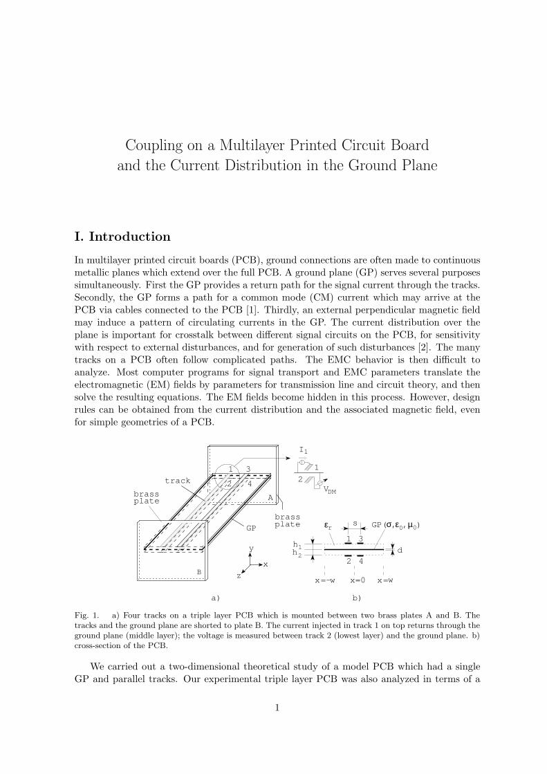
In multilayer printed circuit boards (PCB), ground connections are often made to continuousmetallic planes which extend over the full PCB. A ground plane (GP) serves several purposessimultaneously. First the GP provides a return path for the signal current through the tracks.Secondly, the GP forms a path for a common mode (CM) current which may arrive at thePCB via cables connected to the PCB [1]. Thirdly, an external perpendicular magnetic fieldmay induce a pattern of circulating currents in the GP. The current distribution over theplane is important for crosstalk between different signal circuits on the PCB, for sensitivitywith respect to external disturbances, and for generation of such disturbances [2]. The manytracks on a PCB often follow complicated paths. The EMC behavior is then difficult toanalyze. Most computer programs for signal transport and EMC parameters translate theelectromagnetic (EM) fields by parameters for transmission line and circuit theory, and thensolve the resulting equations. The EM fields become hidden in this process. However, designrules can be obtained from the current distribution and the associated magnetic field, evenfor simple geometries of a PCB.
1
4
3
brassplateGP
brassplate
track
z
x
y
a)
I1
1
2
hh12
d
σ,GP( 0 0)εr s
42
31
=0x=-x =x ww
,µε
b)
VDMA
B
2
Fig. 1. a) Four tracks on a triple layer PCB which is mounted between two brass plates A and B. Thetracks and the ground plane are shorted to plate B. The current injected in track 1 on top returns through theground plane (middle layer); the voltage is measured between track 2 (lowest layer) and the ground plane. b)cross-section of the PCB.
We carried out a two-dimensional theoretical study of a model PCB which had a singleGP and parallel tracks. Our experimental triple layer PCB was also analyzed in terms of a
1

2D-geometry. The GP was the middle layer; tracks were placed at various positions relativeto each other and to the edges of the PCB (Fig. 1). The tracks, the electronic components attheir ends, and the GP form closed signal loops or differential mode (DM) circuits. We aremainly interested in spurious couplings, although the signal transport proper can be analyzedby a similar approach. We replaced all electronics at one end of the tracks by a short circuitto the GP. At the other end we connected one track to a voltmeter which measured the effectof a current injected in another track (DM to DM crosstalk) or injected elsewhere in theGP (CM to DM crosstalk). The ratio of voltage to current can be represented by a transferimpedance Zt. This Zt is related to the current distribution in the GP and the associatedmagnetic field which both depend on frequency in a complicated way. The CM current isinjected through a second plate, e.g. a cabinet panel at some distance under the PCB. We usethe acronym CP for the cabinet panel. Because of reciprocity, the Zt between the CM andthe DM circuits also governs the CM current generation by the DM circuits on the PCB. Forboth DM-DM and DM-CM crosstalk the coupling through the electric field, or the transferadmittance Yt, is not discussed here.
Numerous papers deal with the DM to DM crosstalk between tracks on the same sideof a GP, e.g. tracks 1 and 3 in Fig. 1. Gravelle and Wilson [3] give an extended list ofreferences. Often the high frequency (HF) limit is used, valid above about 30 MHz for acopper GP of 30 µm thickness; above this frequency the current distribution in the GPdoes not change anymore. The HF limit is certainly a good approach when modern highspeed digital electronics is considered. However, there are many important low frequencyapplications such as transducers and amplifiers for slow signals like temperature, level andposition, and electronics for audio and video. Most switched-mode power supplies operate atfrequencies below 1 MHz. At lower frequencies the resistivity of the GP alters the currentdistribution [4].
Both inductive and capacitive coupling are reduced when we place the tracks at oppositesides of the GP. The DM to DM crosstalk is then more sensitive to the current distributionin the GP. Actually we employed this type of crosstalk to study the current distribution inthe GP [5, 6].
The calculations are based on 2D potential theory where we emphasize the coupling by themagnetic field. The tracks were replaced by filamentary wires. We derived general analyticalapproximations for the Zt or the relevant parts thereof, or we present expressions for trackpositions which can be regarded as extreme cases. Such guidelines can help a designer toestimate beforehand the EMC properties of signal circuits. Some integral equations had to besolved numerically. The spurious couplings require considerable accuracy in the calculations;therefore the analytical and numerical results are compared in order to check consistencyand accuracy. In order to retain clarity of the paper, all mathematical details are deferredto Annexes. In Sect. II we discuss a physical picture for the current distribution and theDM-DM crosstalk which provides a simple way to understand the results for an isolatedPCB. Section III describes the calculations and additional results. The Zt for the CM toDM coupling is discussed in Sect. IV. The proximity of a metal cabinet panel influences themagnetic field and alters the DM to DM crosstalk; in Section V we present a choice out ofthe many possible configurations. A signal track between two ground planes and its couplingto another DM circuit outside these planes is studied in Section VI. Section VII presents themeasurements and compares them with the theory. Some practical examples are given inSect. VIII.
The experimental triple layer PCB was 20 cm long. The copper GP had a conductivity
2

σ = 5.8 · 107(Ωm)−1 and a thickness d = 30 µm. The width 2w of the GP was often 50 mm,although wider GP’s were used as well. The 1.5 mm wide tracks were placed at h1,2 = 1.5 mmabove and below the GP (see Fig. 1). The epoxy layer on both sides of the GP had a dielectricconstant εr of 4.7. Two large brass plates mounted perpendicularly at the ends of the PCBformed a mirror for the magnetic field, thus simulating a 2D-geometry. The GP was connectedover the full width to the brass plates; the CP only at one end to allow CM current injection.Measurements are carried out at frequencies between 10 Hz and 1 GHz. The DM-DM Zt’sshow a variety of phenomena below 100 MHz. Resonances in Zt due to the finite length ofthe PCB show up at higher frequencies. In addition, the surroundings of the PCB may affectthe resonances in frequency and in amplitude. Calculations including these 3D-effects are notreported here.
c
dl
z
x
y
I1
a
y=-d
VDM
b
injectioncircuit
circuitsensing
I1 +
-
y=0
Fig. 2. The voltage VDM measured between c and b is determined by the Ez-field along the line a-b and theflux through the area a-b-c-d-a.
II. General behavior of the current distribution and the Zt
between tracks
For a physical picture of the phenomena governing the transfer impedance Zt, we consider theZt(1, 2) between tracks 1 and 2, for the moment centered (x1,2 = 0) on the GP (2w = 5 cm)at opposite sides. The origin of the coordinate system is placed at the center of the uppersurface of the GP. The current I1 is injected in track 1 and returns via the short circuit andthe GP. The DM voltage VDM between track 2 and the GP is determined at the sending endfor the current. Faraday’s law for time harmonic signals
∮E · dl = −jωΦ yields
VDM =b∫
a
Ez(x,−d) dl + jωΦ
= Ez(x,−d)` + jωΦ= ZtI1`, (1)
where Φ is the flux through the rectangle a-b-c-d-a in Fig. 2. The electric field Ez(x,−d) atthe lower surface of the GP is related to the local current density by Jz(x,−d)/σ. The 2D
3

assumption allows the second and third line in Eq. (1); here Zt is the transfer impedance perunit length.
The solid line in Fig. 3a shows the general behavior of Zt(1, 2) for a thin GP without skineffect; Fig. 3b shows the absolute values of the contribution to Zt as calculated in Sect. IIIb:a) Ez(0,−d), and the flux between the GP and track 2 as b) jωΦ1 due to the vacuum magneticfield of track 1, and c) jωΦGP due to the current density in the GP. At low frequencies thevariation of Jz(x, y) with depth y in the GP may be neglected. We can write the volumecurrent density Jz as a sheet current density Kz
Kz(x) =∫ 0
−dJz(x, y)dy, (2)
or simpler here: Kz(x) = dJz(x, y). The Ez is related to Kz through Ez(x,−d) = R2Kz(x),where R2 = 1/σd is the sheet resistance of the GP.
Below 1 kHz (region 1 in Fig. 3a) the current density Kz is also homogeneous in the x-direction. The Zt is given by the d.c. resistance of the GP, Zt(ω = 0) = R2/2w or 11.5 mΩ/mfor our PCB. The vacuum magnetic field due to the current in track 1 and the current inthe GP fully penetrates the GP (Fig. 4a). However, the flux contributions to Zt are stillnegligible. Above 1 kHz the Jz concentrates under the track (Fig. 4b) in order to expel themagnetic field out of the GP. The Ez contribution to Zt(1, 2) increases. At 300 kHz (region3) the current distribution in the GP becomes nearly independent of frequency in the vicinityof track 1. Its value tends to
Kz(x) = −I1
π
h1
x2 + h21
, (3)
analogous to the electrostatic surface charge distribution induced on the GP when a wirewith charge q per unit length is above that plane, see any introductory text book on elec-tromagnetics, e.g. Ramo et al. [7]. The Ez remains related to the Kz. The change in Ez
between region 1 and 3 is a factor 2w/πh1, i.e. a factor 10.6 for our PCB (see Fig. 3b). Theflux contributions lower the change in Zt. The total Zt is constant over nearly two decadesin frequency. Both flux contributions jωΦ1 and jωΦGP become similar in magnitude butopposite in phase. The calculations in Sect. III show that the total flux Φ1 + ΦGP decreaseswith 1/ω, which results in the constant Zt of Eq. (13).
An analogous situation occurs in the more familiar magnetic shielding of a long tube [8]for an external homogeneous axial magnetic field (Fig. 5). An external field He produces aflux through the tube Φe = µ0Heπr2
t . In the tube wall a circulating current It produces aflux LtIt through the tube. Here Lt = µ0πr2
t /`t is the self inductance of the tube regarded asa long single turn coil of length `t. The resistance of the tube for the circulating current isRt = 2πrt/dt`tσt, with dt the wall thickness and σt the conductivity. We again assume herethat the current is homogeneous over the wall thickness. Faraday’s law then results in
RtIt = −jωΦe − jωLtIt. (4)
At low frequencies, ω ¿ Rt/Lt the total flux inside the tube Φe + LtIt ≈ Φe because thecurrent It is low. At high frequencies the flux tends to zero as ΦeRt/(Rt + jωLt). A voltageinduced in a loop inside the tube becomes independent of frequency in this model. The cross-over frequency is given by ωLt = Rt or rtdt = δ2. Here δ =
√2/ωµ0σt is the skin depth for
the tube with µr = 1 because the flux inside the tube is involved rather than the flux in thetube wall. The relation rtdt = δ2 also holds for the onset of shielding against a magnetic field
4

101
frequency in Hz
1
23
4
5
fc
Zt(1-2)
in
Ω/m
103
106
109
10-4
10-2
100
a
b c
0
Ez2whπ 1
101
frequency in Hz
103
106
109
10-6
10-3
100
10
3
jωΦGP
jωΦ1
a)
b)
Fig. 3. a) General behavior of |Zt(1-2)| between track 1 and 2 with a 2w = 5 cm wide GP. The curve 1-2-3-5(—) is calculated by method of moments (Sect. IIIb). The curve 0-2-3-4 (− · − · −) shows |Zt(1-2)| for avery wide ground plane; the skin effect then lowers the |Zt(1-2)| in region 4. The asymptotes a, b and c arediscussed in the text, Sect. III, as is fc = 2.9 kHz from Eq. (5). b) Contributions to |Zt(1-2)| from Eq.(1); Φ1
and ΦGP represent the flux between track 2 and the GP due to the vacuum field of track 1 and of the GP,respectively.
5

50
0
0-50-50
50
x in mm
yinmm
KinA/m
z
0
500-50
50
250
10 Hz 20 kHz 1 GHz
500-50
x in mm500-50
500-50
x in mm500-50
a) b) c)
10 Hz 20 kHz 1 GHz
Fig. 4. Magnetic field lines and current distribution |Kz| in the ground plane (2w = 5 cm) for three frequencies.Only at large distance of the GP the field lines assume the dipolar shape, i.e. closed circles through the dipole.The marked field lines are the separatrices Az = 0 between the field lines, which at large distance close aboveor under the GP.
lt
It
He
dtrt
Fig. 5. Parameters for the tube analogon.
6

perpendicular to the tube axis [9, p. 81]. Returning to our PCB we extend this analogy andestimate the cross-over frequency fc between region 1 and 2 by the relation 2wd = δ2:
fc = R2/2πµ0w (5)
valid for the mid position x ≈ 0 of both tracks. A more accurate estimate requires the solutionof the implicit equation R2 = |Zt| with Zt given by Eq. (12) in Sect. IIIa.
Above 10 MHz two effects become discernible. First the current density approaches theHF limit under track 1 given by Eq. (3). The magnetic field through the GP is stronglyreduced. For an infinitely wide GP, the two flux contributions Φ1 and ΦGP would becomeequal and opposite. However, because of the finite width some magnetic field lines wraparound the GP (Fig. 4c). The flux between track 2 and the GP is then given by the residualdifference of the flux contributions which can be described by a frequency independent mutualinductance M (region 5 and asymptote c in Fig. 3a). From Kaden [9, p. 266] or Love [10,Sect. 13] one has
M =µ0
4π
h1h2
w2, (6)
valid near x = 0 for both tracks. At the edges of the GP Kz(x) approaches the HF limit near|x| = w:
Kz(x) ∝ 1/√
w2 − x2, (7)
analogous to the edge effect for charge density on a plate. The magnetic field near the edgesis strong. However, the current density diverges only in thin strips near the edges of theGP. Because of the small area involved, the flux through these strips is small. Only at highfrequencies the resistance will then be overruled by induction, in our example at frequencieslarger than 30 MHz; the GP then behaves like an ideal conductor (σ →∞).
Secondly, the skin effect alters the vertical current distribution in the GP. For an infinitelywide GP with permeability µ = µrµ0 the high frequency Zt is given by:
Zt = R2
kd
sinh kd
ht
π(x2 + h2t )
, (8)
in which ht = h1+h2 and k = (1+j)/δ with δ =√
2/ωµ0µrσ the skin depth. This behavior isshown by the dot-dash line, region 3 and 4 in Fig. 3a, and by the asymptote b. For the 50 mmwide GP of our example, the exponential decrease in Zt by the skin effect is overruled by theincrease due to the flux coupling around the GP. The transfer impedance of a thin walledtube [9, 11], considered as outer conductor of a coaxial system, decreases in an analogousfashion:
Zt = R0kdt
sinh kdt, (9)
where R0 is approximately the d.c. resistance of the tube per meter, and dt the wall thicknessof the tube. The current flows in the longitudinal direction through the tube wall; thecurrent distribution is axially symmetric. The additional x-dependence in Eq. (8) stems fromthe distribution of the current over the GP. A similar exponential decrease also sets in atdt ≈ δ for the shielding of the tube mentioned above [9, pp. 292-295]. Some authors call thecurrent contraction under track 1 the lateral skin effect or just skin effect [12]. In this paperthe vertical skin effect is meant when the term vertical is omitted.
Note that the perpendicular component H⊥ of the magnetic field at the surface of the GPnever vanishes exactly for a GP with finite conductivity. The y-component of ∇×E = −jωB
7

links the x-variation of the current density σEz to the H⊥. In region 3 (Fig. 3a) the magneticfield penetrates the GP and leaves at the other side of the GP; in region 4 the magnetic fieldH⊥ at the surface is guided through the skin. The penetration is more pronounced where thevariation of the current density is larger, i.e. near the edges and under track 1 as discussedbefore.
III. Mathematical description
a. The half space and the infinite plate
In a first step consider the plane y = 0 limiting the lower half space (Fig. 6a) of materialwith conductivity σ and magnetic permeability µ = µ0µr. The filamentary wire carrying theinjection current I1 is in the dielectric region (ε0, µ0) at a height h1 above the plane. Thedistribution of the induced return current Jz(x, y) in the plane has already been calculated byCarson [13] in 1926 for non-magnetic materials (µr = 1). He assumed a transverse magneticwave ∝ ejωt−γz propagating in the positive z-direction with a small propagation constant γ.
dh1
2w
h2
x2
x1
d h1
h2
xx=0 x
y
σ,ε 0
0σ,ε
h1ε 0 0
a)
b)
c)
y=0
y=0y=-d
2
,µ
,µ
,µ
Fig. 6. Parameters for a) the infinite plane, b) the infinite plate, and c) the strip or finite plate.
Carson aimed at a telegraph wire several meters above soil with typical conductivity ofabout 10−2 (Ωm)−1. Many authors [14, 15, 16, 17] treated the transmission of waves alongwires above a dissipative medium; some use the full wave analysis. For our PCB Carson’sapproach is apparently correct up to the GHz range because of the much smaller distances
8

between tracks and GP and the high conductivity of copper. Appendix A1 gives the generalsteps of Carson’s derivation, which is slightly extended in order to incorporate magneticmaterials µr 6= 1; see also [18].
In a second step consider the plate at y = 0 with thickness d and conductivity σ, stillof infinite extent in the x-direction (Fig. 6b). The injection wire is at the position (0, h1)above the upper side of the plate; a sensing wire is at (x2,−h2) below the plate. In bothdielectric regions µr = 1 is assumed. Since we do only consider the coupling by the Zt, we mayalso take εr = 1. Because of the finite conductivity, the magnetic field penetrates the plate.An inductive coupling exists between the circuits at both sides of the GP. In Appendix A2,Carson’s calculation for the longitudinal current distribution Jz(x, y) in the plate is extendedto allow a finite thickness d of the plate (Eq. (A13)) and to include the magnetic field belowthe plate.
For a thin GP one may take the ‘thin plate limit’ d ↓ 0 and σ → ∞ while keeping thesheet resistance R2 of the plate constant. The sheet current density Kz can be derived fromthe current density Jz(x, y) in Eq. (A13):
Kz(x) =∫ 0
−dJz(x, y) dy = −jωµ0I1
2πR2
∫ ∞
0
cos(αx) e−αh1
α + jβdα, (10)
in which β = ωµ0/2R2. Asymptotic expressions for Zt can also be derived in closed form.After some algebra using Eq. (A17), the transfer impedance for the sensing wire at (x2,−h2)under the GP simplifies to
Zt =jωµ0
2π
∞∫
0
cos(αx2)e−αht
α + jβdα, (11)
in which ht = h1 + h2. For low frequencies the small argument expansion [19] of the Eifunctions in Eq. (A18) yields
Zt =14ωµ0 − j
ωµ0
2π
[ln
ωµ0(x22 + h2
t )12
2R2
+ γ
], (12)
with γ = 0.57721 · · · Euler’s constant. This Zt is the asymptote labeled a in Fig. 3a. Thehigh frequency approximation of Eq. (11) reduces to
Zt = R2
ht
π(x22 + h2
t ). (13)
This Zt value (region 3 and asymptote b in Fig. 3a) does not explicitly depend on the frequency.In Eq. (11) only the sum ht of the heights h1 and h2 occurs. Reciprocity only requires thatthe Zt is symmetrical in h1 and h2. Remarkably the position of the thin GP between thetrack does not influence this part of Zt.
In the thin plate limit no skin effect is possible since d/δ goes to zero. In order to correctlydescribe the skin effect we must consider a general thickness d and use the full equation (A17).The resulting Zt is displayed as curve 0-2-3-4 in Fig. 3a. Fortunately the expression simplifiesin the high frequency limit to Eq. (8). The frequency fcs where the skin effect becomeseffective, can be calculated explicitly. Choose, by convention, the 3 dB point where |Zt|2
9

obtained by Eq. (8) is halved with regard to the value of region 3 in Fig. 2 given by Eq. (13).The transcendental equation ∣∣∣∣sinh
[(1 + j)
d
δ
]∣∣∣∣ = 2d
δ, (14)
has an approximate solution d/δ ≈ 2.14. Thus the cutoff frequency fcs is given by
fcs ≈ 2.25πµ0σd2
, (15)
and is again independent of the heights h1 and h2. This frequency equals approx. 22 MHzfor the GP parameters used in calculating Zt in Fig. 3a. In Fig. 3a the curve 0-2-3-4 showsthe behavior of Zt as described in this Section. Good agreement is shown in region 2 and 3(Fig. 3a) between the analytical expressions and the method of moments (MOM) calculations[20] described in the next subsection. The deviations at the low and the high frequency end(region 1 and 5 in Fig. 3a) are due to the finite width of the GP.
b. The strip of finite width
We now replace the infinite plate GP by a strip of width 2w (Fig. 6c). The injection currentI1 flows through the wire at the upper side of the strip and returns via the strip. We againconsider the thin plate limit and calculate the sheet current density Kz(x). The width 2w isless than the shortest wavelength under consideration. We use Faraday’s law for two positions(x, 0) and (x∗, 0) on the strip:
Ez(x, 0)− Ez(x∗, 0) = −jω Az(x, 0)−Az(x∗, 0) (16)
in which the vector potential Az is due to the current I1 through the injection wire and tothe current Kz = Ez/R2 distributed over the strip, see Appendix B. Here we require that I1
returns through the strip, orw∫
−w
Kz(x) dx = −I1, (17)
Equation (16) was solved by the method of moments [20]. Step functions as basis functionsapproximated Kz(x) over intervals of the strip. Point-matching (Dirac delta functions astesting functions) was used. The collocation points were at the middle of subsequent intervals.The vector potential contribution due to each interval was calculated analytically [21]. Inorder to improve the accuracy with reduced calculation effort, the discretization of the stripwas non-uniform: a (x2 +h2
1)−1 partition beneath the injection wire and a fine constant mesh
at the edges. The transfer impedance Zt is then obtained by Eq. (1). The solid line in Fig. 3ais obtained by this MOM method. The total number N of intervals was chosen in such a waythat the difference between the analytical HF value of Zt (see next section) and the numericalone was less than 10 percent. This required an accuracy in the Az of about 10−4; comparealso Fig. 3b. Such accuracy is generally needed in EMC calculations because one looks forspurious couplings close to the currents. No attempts were made to obtain the ‘ideal mesh’through rigorous error analysis.
For low frequencies the resistive contribution (Ez term in Eq. (1)) dominates the magneticflux term, and Zt is constant. The cross-over frequency fc between region 1 and 2 wasdiscussed in Sect. II; an approximate expression based on the tube analogon is given in
10

Eq. (5). The flat region 3 agrees with the analytical expression Eq. (13) for Zt presentedbefore. At high frequencies the vector potential dominates the resistive term; the l.h.s. ofEq. (16) can be neglected. As a result of the finite width, the transfer impedance in Fig. 3increases linearly with frequency for f > 30 MHz.
When both tracks are close to the edge, the current density concentrates more slowlyunder track 1; the calculated Zt is shown in Fig. 7. At high frequency the MOM Zt is inagreement with the analytical expression Eq. (20) discussed below.
101
103
106
109
frequency in Hz
10-3
100
103
Zt
in
Ω/m
Fig. 7. DM to DM Zt calculated by MOM for one or both wires at the edge of a 50 mm wide GP. The verticaldistance between wires and GP is 1.5 mm. The straight line behavior above 10 MHz corresponds to M -valuesof Fig. 8.
c. Mutual inductance
For high frequencies the GP can be considered as an thin (d ↓ 0) ideal conductor (σ → ∞)with a sheet current distribution Kz. The magnetic field does not penetrate the GP anymore.The magnetic field outside the GP can then be derived from a complex potential Ω whichcan be obtained by means of conformal transformation. See for details Appendix C1. Thecurrent distribution on both surfaces of the strip results from [9, pp. 56-58]
Kz(x) = −|y ×H| = −RedΩ∗
dz, (18)
where Ω∗ is the conjugated of the complex potential Ω. For an arbitrary position of theinjection wire, the result of Eq. (18) is given by Love [10]. For small height-to-width-ratioh1/w and the injection wire near x = 0, his solution [10, Sect. 13] can be approximated by
Kz(x) ≈ −I1
π
[h1
x2 + h21
+h1
w√
w2 − x2
], (19)
in which the contribution of Ω at the upper and lower surface are added (see Fig. C1). Thefirst term of the right hand side is the same as the HF distribution for an infinitely thin plate;compare with Eq. (3). The last term results from the edge effect.
11

innH
-25 0 25
x in mm
10-1
103
101
/m
M
Fig. 8. The mutual inductance part M of Zt between two DM circuits when one of the circuits moves overthe GP along the x-direction. Both tracks are at 1.5 mm distance from the 50 mm wide GP.
The transfer impedance now becomes a frequency independent mutual inductance Mwhich can be calculated by means of Eqs. (C1), (C3), (C4), and (C5) for any position of thetwo wires. When h1,2 ¿ w simple real forms exist. The lowest M is given by Eq. (6) for bothwires at x = 0 on opposite sides of the GP. An upper bound occurs when both wires are atthe same edge, |x| = w, but still on opposite sides of the GP. For general h1 and h2:
M(|x| = w) ≈ µ0
4πln
[1 +
2√
h1h2
(h1 + h2)
], (20)
which attains a maximum value when h1 = h2: M2 = (µ0/4π) ln 2. Figure 8 shows a set ofM -curves for a GP of 2w = 5cm and both wires at the same distance h1,2 = 1.5 mm w.r.t. tothe GP, calculated from the full complex potential Ω of Eq. (C4). For comparison we includedan M -curve for both wires on the same side of the GP, one of them placed at x = 0.
IV. Common mode to differential mode coupling
The DM circuits on a PCB may generate a CM current which flows along the cables connectedto the PCB. We consider the reciprocal setup, a CM current ICM through the GP whicharrives through a second plane such as a cabinet panel (CP) may provide (Fig. 9). TheCM current distribution and the Zt with respect to the DM circuit is calculated. Severallimiting situations can be considered: the CP a) has a certain width 2p or b) is very largein the x-direction; the CP is c) nearby (hCP /w ¿ 1) or d) at a large distance from the GP(hCP /w →∞). In the experiments we used a brass plate as CP of thickness dp = 1.5 mm andwidth 2p = 20 cm. We assume the thin plate limit for both CP and GP. The CP is usuallylarger than the GP. Induction currents reduce the magnetic field through the CP alreadyat low frequencies; edge effects and skin effect are less important. Most calculations were
12

performed by the MOM. The sensing wire 1 is again placed at the distance h1 = 1.5 mm fromthe GP (2w = 5 cm).
hCP
dp
dh1
2w
2p
GP
CP
x
y=0
Fig. 9. Parameters for the PCB above a cabinet panel (CP).
101
103
106
109
frequency in Hz
10-3
100
102
Zt
in
Ω/m
Fig. 10. CM to DM Zt when the CP is far away (- - -), or at hCP = 1 cm distance from the GP (—). Thetrack is at 1.5 mm above or under the GP.
First we consider the CP at a large distance from the GP (see Fig. 10). At d.c. or lowfrequencies Kz = ICM/2w holds and Zt = R2/2w is equal to the d.c. resistance of the GP.Above a frequency fc given by 2wd ' δ2 [22] the current density Kz(x) adjusts to reducethe penetration of the magnetic field through the GP; Kz(x = 0) decreases towards the highfrequency value ICM/πw [9, p. 63]. For the GP width chosen, the corresponding decreasein Zt by a factor 2/π does barely occur. At high frequencies Zt becomes inductive; M wascalculated by conformal transformations, Appendix C3, Eq. (C9) where the injection wirewas placed at a large distance. We again compare the M(x, y)-values for the sensing wire 1
13

at x = 0 and at |x| = w:
M(0, h1) ≈ µ0
2π
h1
w(21)
M(|x| = w, h1) ≈ µ0
2π
√h1
w. (22)
These expressions for M present two bounds, and are accurate to within 10 percent for thetrack at either side of the GP when h1/w < 0.9.
Secondly, we place the 20 cm wide CP at the distance hCP = 1 cm under the GP, atypical value often encountered in practice. The Zt for several positions of the sensing wire 1calculated by MOM is given in Fig. 10. Examples of magnetic field lines are shown in Fig. 11.
-50 0 50-50
0
yinmm
5010 Hz 1 GHz
-50
0
yinmm
50
in mmx
-50 0 50
in mmx
Fig. 11. Magnetic field pattern at low and at high frequency for a CM current through the CP (2p = 20 cm)which returns via the GP (2w = 5 cm).
At high frequencies the nearby CP (hCP /w ¿ 1) causes a homogeneous H-field under theGP and a strongly reduced field above the GP. The Zt now depends on which side the sensingwire is placed. Because of the homogeneity of the field under the GP, a first approximationfor M(x, y) at x = 0 and y = −h1, assuming hCP /w ¿ 1, is:
M(0,−h1) ≈ µ0h1
2w, (23)
a factor π larger than Eq. (21) for the isolated PCB.At other positions of the track 1 the M -values are more difficult to obtain. In principle,
the magnetic field and M can be calculated by means of conformal transformation. Love [10]gave the general Schwarz-Christoffel transformation consisting of elliptic functions; his resultswere extended by Langton [23] and Lin [24]. This method only gives an implicit solution. Forthe position (x, y) = (0, h1) above the GP, expansion of the elliptic functions (Appendix C4)results in
M(0, h1) ≈ µ0h1hCP
πw2(24)
14

which is a factor 2hCP /πw smaller than the M at the lower side of the GP, Eq. (23). Forother positions, e.g. at the edge of the GP |x| = w, we proceed in a different and approximateway. For hCP ¿ 2w the other edge may be thought infinitely far away. The H-field nearone edge can then be derived from a simpler transformation which is often employed for thefringing field of a parallel plate capacitor [7, Sect. 7.7]. The solution is still implicit (seeAppendix C5), but involves only an exponential. For h1 ¿ hCP the first two terms in theexpansion of the exponential result in:
M(|x| = w, |y| = h1) ≈ µ0
2w
√h1hCP
π(25)
irrespective on which side of the GP track 1 is placed. Already for h1 ' hCP /10 higher orderterms in the expansion become discernible. A numerical fit to the calculations resulted in acorrection term
∆M(|x| = w, y) ≈ µ0
2wc1y (26)
with c1 ' −1/3, in which y is positive for positions above the GP. This ∆M restores theactual asymmetry between upper and lower positions of the track 1; for a more elaborate fitsee Appendix C5 and Fig. C4. The variation of M(x, h1) and M(x,−h1) over the width of aGP is shown in Fig. 12a, whereas Fig. 12b gives the M as function of hCP /w for a few fixedpositions of the sensing wire. For this GP size and position (2w = 5 cm, hCP = 1 cm) theassumption hCP /w ¿ 1 is not fulfilled, and the actual magnetic flux between GP and CP islower than assumed. The current distribution Kz(x) in the GP and the total flux betweenGP and CP calculated by MOM agreed well with the analytical expression for parallel stripsgiven by Kuester and Chang [25, Eq. 6]. For wire 1 close to the GP, we corrected the M -valuesgiven above by the ratio of the total flux given in [25] and the flux of a assumed homogeneousfield µ0ICMhCP /2w; see Appendix C5 at the end.
V. Influence of the CP on the DM to DM crosstalk
When the cabinet panel approaches the ground plane, the magnetic field due to the DMcircuit induces a circulating current in the CP even without net current flow in the CP. TheDM to DM crosstalk depends on the position of the CP. For a disconnected CP, Fig. 13ashows the Zt(1-2) at several hCP , with both tracks at mid GP (x1 = x2 = 0). We againassumed h1 = h2 = 1.5 mm and 2w = 5 cm.
Of course the Zt at d.c. does not depend on the presence of the disconnected CP. At midfrequencies, region 3 of Fig. 3a, the Zt is only reduced when track 2 is very close to the CP.The Zt assumes the behavior of an isolated PCB already for distances hCP of 1 cm. At highfrequencies the field lines wrapping around the GP dominate the Zt. For smaller distanceshCP the H-field under the GP is compressed, leading to higher M -values. The homogeneity ofthe field improves, and the M -values for x2 = 0 and |x2| = w (lowest two curves in Fig. 13b)converge. At hCP = 1.5 mm these M ’s are equal since both DM circuits then capture allmagnetic flux under the GP. The field lines at the edges (see e.g. Fig. 11) show less curvaturefor smaller hCP , as is demonstrated by the lower M for the sensing track above the GP.
We now connect the GP to the CP over their full width at both ends. A current ICM
flows in the closed CM loop, induced by I1 in the DM circuit formed by wire 1 and the GP.
15

0 25100
102
101
innH/m
x in mm
0
in mm
100
102
hCP
101
+
+
++
20 40 60
a)
MinnH/m
b)
M
Fig. 12. a) Mutual inductance M between CM and DM loop when the x-position of the track varies over theGP (full width 5 cm). The 20 cm wide CP is at hCP = 1 cm under the GP. The circles are MOM results, thesolid lines are analytical approximations discussed in Appendix C5. The three markers on the right ordinateindicate the M -values at the edge. The middle one is M from Eq. (25), to which the correction ∆M fromEq. (26) has been added or subtracted. The markers on the left ordinate correspond to Eq. (24) and Eq. (23)without further correction. b) Mutual inductance M between CM and DM loop as function of hCP for fourpositions of the sensing track. The measurements (Sect. VII) at hCP = 1 cm and 6 cm are indicated (+). Theupper marker at the right ordinate corresponds to Eq. (22), the lower to Eq. (21).
16

hCP
1.52
3
∞
10
101
103
106
109
frequency in Hz
10-2
100
Zt
in
Ω/m
0 25 50
innH/m
10-1
102
100
101
in mmhCP
a)
b)
M
Fig. 13. a) DM to DM Zt for several distances hCP (in mm) between GP (2w = 50 mm) and CP (2p = 20 cm).b) M -part of Zt for DM to DM, as function of hCP for several positions of the injection and sensing tracks.
Both DM and CM loop couple via the transfer impedance Zt(1-CM), given in the previousSection (see Fig. 10) for the reciprocal situation CM-1. We have
I1Zt(1-CM) + ICMZCM = 0, with ZCM = RCM + jωLCM . (27)
The selfinductance of the CM loop LCM , as well as the distribution of ICM over the GPand CP can be calculated by the MOM, which agreed with the analytical approximations ofKuester and Chang [25]. The RCM is the series resistance of GP and CP. The final transferimpedance between the tracks 1 and 2 is denoted by Zt(1-2,c) where c indicates the closedCM loop:
Zt(1-2,c) = Zt(1-2,o)− Zt(1-CM)Zt(2-CM)ZCM
(28)
with Zt(1-2,o) the transfer impedance in case of an open CM loop. Figure 14 shows Zt(1-2,c),assuming a CP of 1.5 mm brass in which the skin effect is neglected, hCP = 1 cm, h1 = h2 =1.5 mm and 2w = 5 cm.
17

101
103
106
109
frequency in Hz
10-4
100
102
Zt
in
Ω/m
10-2
hCP
Fig. 14. The MOM results of the DM to DM Zt (—) when the CP (2p = 20 cm) is connected to the GP(2w = 50 mm) at both ends; hCP = 1 cm. Also indicated are the Zt for a disconnected CP (· · ·), as well asthe expected behavior due to the skin effect and due to the residual M -coupling (- - -).
Major changes occur at low frequencies; the small resistance RCP of the CP is parallelto RGP of the GP, and Zt = RGP RCP /(RGP + RCP ). However, already at 100 Hz the Zt
rises. In order to estimate the cross-over frequency from Eq. (28), one may replace ZCM byRCM + jωLCM and substitute both Zt(1-CM) and Zt(2-CM) by RGP . In first approximationZt(1-2,o) also equals RGP . The resulting cross-over frequency becomes LCM/2πRCP , whichfor our setup is 230 Hz. The small inductive component in Zt(1-2,o) is mainly responsible forthe lowering of the cross-over to about 100 Hz as apparent from Fig. 14. The flat region 3 isextended to higher frequencies. The short circuited CM loop reduces the flux and decreasesthe M-coupling. The dotted lines indicate the residual M-coupling, as well as the expecteddecrease due to the skin effect in the GP.
VI. A DM track between two planes
In multilayer PCB’s the coupling of a signal track is reduced when the track is placed betweentwo planes, ground and/or power; assume the planes at y = ±hPP (Fig. 15). We first describethe Zt between a track on top of a very wide PCB and a track midway between both planesat (x1, y1) = (0, 0) carrying a current I1. Assuming very wide GP’s and filamentary wires forthe tracks, the current distribution Kz in both planes can be calculated as in Sect. III, seeAppendix A3. The ‘thin plate’ result is:
Kz(x) = −jωµ0I1
2πR2
∫ ∞
0
cos(αx) e−αhPP
α + jβ(1 + e−2αhPP )dα, (29)
with β = ωµ0/2R2 again. The high frequency Kz becomes
Kz(x) = − I1
4hsech
πx
2hPP, (30)
18

d
y=d hPP
y=-hPP
y =0
x=0
x = wx =-w
x( 2 2),y
x( 1 1),y
Fig. 15. Parameters for a wire 1 between two planes of width 2w. The sensing wire 2 resides outside the twoplanes.
which is a factor π/4 smaller than the current density at x = 0 with only one GP; compareEq. (3). The current density is also more concentrated near wire 1. For the ‘thin plate’ Zt ofa wire at (x2, h2) with h2 ≥ hPP
Zt =jωµ0
2π
∫ ∞
0
cos(αx2) e−αh2
α + jβ(1 + e−2αhPP )dα, (31)
which describes regions 0, 2, and 3 in Fig. 16. We include the skin effect (region 3 and 4 inFig. 16) to obtain the high frequency Zt:
Zt =R2
π
kd
sinh kd
∫ ∞
0
cos(αx2) eα(d−h2)
1 + e−2αhPPdα. (32)
The integral can be expressed in elementary Ψ-functions [26, 3.541.6]. For (x2, y2) = (0, 2hPP )and d ↓ 0 the integral is simply (ln 2)/2hPP . In the flat region 3 Zt is a factor ln 2 smallerthan the Zt with one GP, Eq. (8), at the equivalent position. However, because a part of thecurrent returns at the other side of wire 1, the reduction in Zt is less than 1/2 as could beexpected naively.
When the injection wire is midway between the planes, the return current is shared equallyby both planes. For other y-position of the wire, the total current varies linearly as −(hPP +y)I1/2hPP for the top and as −(hPP − y)I1/2hPP for the bottom plane at high frequencies.
The M -part in Zt is strongly reduced since both planes effectively confine the magneticfield. An approximate procedure again has been followed assuming that wire 1 and 2 are atsome distance |δx1| and |δx2| from the edge of the PCB; see Appendix C6. For M one finds:
M =µ0 δh2
2π
(hPP
π|δx2|3) 1
2
e−π |δx1|2hPP
− 12 , (33)
where δh2 is the vertical distance of wire 2 above the top plane. Because of the exponentialin δx1 only one edge is taken into account. In Fig. 17 we compare Eq. (33) with the complexpotential result of Eq. (C25). When wire 1 is deeply buried between both planes at large δx1,very low M -values result by Eq. (33) and other effects may become dominant. Assume forinstance that the planes provide of ground and d.c. power; insufficient decoupling between
19

101
frequency in Hz
Z tin
Ω/m
103
106
109
10-4
10-2
100
1
23
4
5
0
Fig. 16. General behavior of |Zt| between track 1 and 2 with 2w = 5 cm wide planes. Track 1 is positioned atthe origin, while track 2 resides at (0, 2hPP ), width hPP = 1.5 mm. The solid curve 1-2-3-5 has been calculatedby means of MOM; the deviation in region 5 is due to numerical errors. The curve 0-2-3-4 (- - -) shows |Zt|for very wide planes; the skin effect again lowers the impedance in region 4. For comparison we have includedthe behavior for a PCB with only one GP.
the planes at the ends may cause a different return current −(12 ± a)I1 through the top (+)
and bottom (−) plane. The value of a has to be estimated for an actual PCB; here we justassume any value 0 ≤ |a| ≤ 1
2 . In worst case, no net return current flows through either ofthe planes. This situation is comparable to Section IV for a ‘CM’ current a I1; the results ofEqs. (24) and (25) can be multiplied by a, with hPP substituted for hCP .
VII. Measurements
The three layer PCB (Fig. 1) consisted of a single and a double layer PCB firmly pressedagainst each other. On each side of the GP two 1.5 mm wide tracks (Fig. 1) were placedat s = 10 mm apart. Brass plates (30 × 20 cm2) at both ends of the combined PCBminimized distortion of the 2D-fields due to end-effects. SMA-connectors with low proper Zt
were mounted in one of the brass plates (A in Fig. 1). In order to avoid Zt-contributionsfrom the cables and the measuring equipment, the brass plate A was properly connected tothe backpanel of an EMC-cabinet [27] in which the measuring equipment resided. The cableswere RG223 with double braided shield; several ferrite cores kept the CM currents throughthe cables sufficiently low.
Between 10 Hz and 100 kHz a sinewave generator provided the injection current which wasmeasured by an active current probe. The generator was placed outside the EMC-cabinet. Alock-in detector inside that cabinet determined the DM voltage in amplitude and phase; seee.g. [28]. The output of the current probe served as reference. Between 200 kHz and 1 Ghz weemployed a spectrum-network analyzer; the tracking generator provided the injection current.Up to 50 MHz an inductive current probe measured the current directly at the input connectoron the brass plate A. Above 50 MHz an S-parameter set was used to determine the injection
20

-25
in mm
10-1
102
x
100
0
2
101
25
innH
M/m
Fig. 17. The mutual inductance part M of Zt between two DM circuits. The injection wire resides betweenthe two finite planes, near the edge. The sensing wire at the upper plane moves over the full width. The fullexpression Eq. (C24) (—) as well as the approximations Eqs. (33) (· · ·) and (C25) (− · − · −) are shown
current at the input SMA connector of the PCB.We present measurements of DM-DM crosstalk which demonstrate the current distribu-
tion. Figure 18 shows the Zt for an isolated PCB with current injection in track 1, and track 2and 4 as sensing tracks (see Fig. 1). Up to 70 MHz measurements and calculations agree. Thecurrent contraction under track 1 (region 3 in Fig.3a) causes |Zt(1-2)| to rise and |Zt(1-4)|to decrease. The M -coupling (region 5) is nearly the same for track 2 and 4, as indicatedby the convergence of the Zt curves above 10 MHz. The frequency of the resonance peaksin Zt agree with standing waves in injection and sensing circuit over the length ` = 0.2 m:` = (2n + 1)λ/4 with n = 0, 1, 2, .... Here λ is the wavelength calculated with an effectivedielectric constant εr,eff = 3.41 [7, Sect. 8.6]. For this slender GP the skin effect does barelyshow up because of the predominant M -coupling and because of the resonances.
The Zt for one or both tracks at the edge of the GP is shown in Fig. 18b. The width ofthe GP is 2w = 15 cm. Here too, measurements and calculations agree up to the resonances.
The measured and calculated CM to DM crosstalk is presented in Fig. 19 for the midposition of the sensing track. The current was injected in the CM loop through the CP, andreturned through the 5 cm wide GP. Two distances hCP of 1 cm and of 6 cm were used.The experimental M-values are included in Fig. 12. Standing waves occur as in the DM-DMcrosstalk. The frequency of the low-Q shoulder on the first peak varies with hCP . Thisresonance probably originates in the current injection circuit.
VIII. Conducted emission
We apply the transfer impedance Zt(DM-CM) to describe the emission due to a CM currentthrough a cable connected to the model PCB. The current waveform in the DM circuit aretypical choices for a switched-mode power supply and for several families of logic circuits
21

101
103
106
109
frequency in Hz
10-3
100
103
Zt
in
Ω/m
101
103
106
109
frequency in Hz
10-4
100
104
Zin
Ω/m
a)
b)
t
Fig. 18. a) The measured DM to DM |Zt(1-2)| and |Zt(1-4)| (—) together with the MOM calculations(· · ·). Tracks 1 and 2 are on opposite sides at 5 mm from the middle line of the GP (2w = 5 cm); thex-distance between track 1 and 4 is s = 10 mm. The resonances above 100 MHz are discussed in the text. Theactual reduction of |Zt(1-2)| due to the skin effect occurs at lower frequencies than expected (- - -), becauseof the opposite phase in the couplings by the skin effect and by the inductive M -coupling, see e.g. Kaden [9,Fig. 171]. b) Measured (—) and calculated (- - -) DM to DM |Zt| with one or both tracks at the edge of theGP (2w = 15 cm).
22

101
103
106
109
frequency in Hz
10-3
100
103
Zt
in
Ω/m
Fig. 19. Measured (—) and calculated (- - -) CM to DM Zt for two positions of the sensing track; hCP = 1 cm,2w = 50 mm, h1 = 1.5 mm.
(Fig. 20). In the model we connect the GP at one side to the CP (inset Fig. 21). The cable isrepresented by a half wave antenna with a radiation resistance R0 = 150 Ω. This resonancecondition may not occur at all frequencies in the DM signal, but will most probably do soat some frequency for which the emission limits might then be exceeded. When propagationdelays over the PCB are neglected, the induced CM voltage vind(t) can be imagined as alocalized source between cable and GP which drives the cable as antenna. The CM currentiCM (t) through the cable at resonance is then given by vind(t)/R0.
tf TH tr
T
∆i ∆ i
tf tr
b)
* *
∆ if
r
a)
0
Fig. 20. Typical current waveforms for a) switched-mode power supplies and TTL and ECL digital circuits,b) for fast CMOS circuits.
The DM current waveforms in switched-mode power supplies or TTL and ECL digitalcircuits is approximated by the trapezoids in Fig. 20a. For CMOS and similar circuits, theDM current resembles more a triangular shape (Fig. 20b). The trapezoidal current iDM (t) is
23

expanded in the Fourier series
iDM (t) =∞∑
n=−∞IDMn ejnω0t, (34)
with ω0 = 2πf0 = 2π/T0. For tr = tf = τ the coefficients IDMn are given by
IDMn = ∆i
sin(nω0τ/2)nω0τ/2
sin[nω0(TH + τ)/2]nπ
. (35)
The transfer impedance Zt(DM-CM) can be approximated by
Zt(ω) ≈ RGP + jωM. (36)
The induced voltage vind(t) then follows from
vind(t) =∞∑
n=−∞V ind
n ejnω0t, (37)
withV ind
n = Zt(nω0)IDMn . (38)
According to the EN55022 regulation, the maximum electric field strength should notexceed 30 dBµV/m (at 10 m for class B equipment) in the frequency range 30-230 MHz. Thisrequires a CM current through the cable of less than 3 µA, see e.g. Ott [29] or Goedbloed[30, Sect. 2.4.1].
The fundamental frequency f0 determines the minimal harmonic number m in Eq. (34)for which the EMC requirements should be met. The corresponding spectral component ofiCM (t) is ICM
m = V indm /R0 when the resistance term in Zt is neglected. The upper bound for
the amplitude of this spectral component is given by
|ICMm | ≤ 4M ∆i
πmR0τ, (39)
which hold for the waveform given in Fig. 20a. For the waveform given in Fig. 20b, τ mustbe replaced by mint∗r/2, t∗f/2 and ∆i by max∆ir, ∆if.
In Table I, |ICMm | is given for a few families of digital circuits. As can be seen, the 3 µA
limit for ECL3 and HLL digital logic requires extensive EMC measures. A reduction of about44 dB and 65 dB respectively should be obtained in case of our 0.2 m long and 5 cm widePCB, for instance by an extra ground plane or cabinet panel, smaller distances between tracksand GP, filter connectors, etc.
We tested these calculations in a setup which is often used for precompliance measurements[31], see Fig. 21. The CM current is generated by the DM circuits above (track 1, Fig. 1) orunder (track 2) the GP. This CM current is measured at the 150 Ω load, formed by the 100 ΩSMD-resistor and the 50 Ω impedance of the cable connected to the spectrum analyzer. Forour 5 cm wide and 20 cm long PCB, the ratio of the DM and CM currents is given in Fig. 21,measured as well as calculated.
24

Table I. Upper bounds for the maximal spectral components of iCM given by the r.h.s. of Eq. (39). Forthe switched-mode power supply (SMPS) and ECL3 (or ECL-100K) digital logic, the trapezoidal waveform(Fig. 20a) is used; a triangular shape form (Fig. 20b) is assumed for CMOS and HLL logic. The mutualinductances M are calculated by MOM (Sect. IV.).
max|ICMm | in µA per length of PCB
2w = 5 cm 2w = 15 cmTYPEinjection 1 injection 2 injection 1 injection 2
f0/τ/∆iM = 4.8 nH/m M = 24.9 nH/m M = 0.6 nH/m M = 10.6 nH/m
SMPS100 kHz/100 ns/1 A
1.4 7.0 0.2 3.0
ECL3 (ECL-100K)230 MHz/1.3 ns/14.8 mA
463.9 2406.2 58.0 1024.3
CMOS10 MHz/60 ns/4.2 mA
2.9 14.8 0.4 6.3
HLL (CMOS 3V)230 MHz/1.5 ns/100 mA
5432.5 28181.0 679.1 11996.7
105
106
107
109
frequency in Hz
10-5
101
ICM
I1,2
/
108
10-3
10-1
VDM
100GP1
2I1
50
ICM
Fig. 21. Measured (—) and calculated (- - -) current transfer between DM and CM circuits, for a DM injectiontrack above (1) or below (2) the GP. The inset shows the setup for precompliance measurements with currentinjection through track 1. The CM current is measured via the 150 Ω load.
25

IX. Concluding remarks
The M -part in the DM to DM crosstalk shows a strong dependence when one or both tracksare near the edges of the GP. A distance of 3h1 reduces the crosstalk by about one order ofmagnitude. For distances hCP of 1 cm and more between GP and CP, the influence of theCP on this cross-talk nearly vanishes.
When a CP is present under the GP, the M -part of the CM to DM crosstalk is lowestfor traces at the upper side of the GP. Even for our slender PCB this difference is about oneorder of magnitude. For traces at the edges the difference between upper and lower side issmaller.
In our analysis we used 1.5 mm thick insulation. Many multilayer PCB have also interlayerinsulations of 0.2 mm, and correspondingly smaller tracks and track distances. There is alsoa tendency to reduce the copper layer thickness. For such PCB’s the analytical expressionsfor Zt are valuable.
In a PCB with more than one ground plane or power plane the DM return current willbe shared by those planes. A 2D analysis of such sharing can be carried out in a similar wayas presented. The current distribution also depends on the action of e.g. the logical circuits,whether they switch the signal lead to ground or to power. The position of decouplingcapacitors between the planes is then also important.
26

Appendix A
1. Carson’s approach
A filamentary wire 1 is positioned at x = 0 in a dielectric region at the height h1 aboveconductive ground which fills the lower halfspace y < 0 (Fig. 6a). The wire carries a currentwave I1 propagating as ejωt−γz in the positive z-direction. The propagation constant γ istaken small. The Ex and Ey components of the electrical field are neglected, as well as thedisplacement current in the ground. The equation
∇2Ez = jωµσEz (A1)
holds for time harmonic fields in the GP. Under the assumptions mentioned Carson’s solution[13] of Eq. (A1) is the Fourier cosine integral w.r.t. x
Ez(x, y) = −∞∫
0
F (α) cos(αx) ey√
α2+jωµσ dα. (A2)
The x and y-components of the magnetic field H in the ground stem from Maxwell’s equation∇ × E = −jωµH, in which µ = µ0µr. Above ground the current I1 produces the familiarr−1-field H1 and the current distribution Jz(x, y) = σEz(x, y) produces a magnetic field H2
with transverse components only. Expand both magnetic fields in Fourier cosine integrals(x-components) and Fourier sine integrals (y-components):
H1x =I1
2π
h1 − y
x2 + (h1 − y)2
=I1
2π
∫ ∞
0cos(αx) e−α(h1−y) dα,
H1y =I1
2π
x
x2 + (h1 − y)2
=I1
2π
∫ ∞
0sin(αx) e−α(h1−y) dα, (A3)
H2x = +∫ ∞
0[φ(α) +
I1
2πe−αh1 ] cos(αx) e−αy dα,
H2y = −∫ ∞
0[φ(α) +
I1
2πe−αh1 ] sin(αx) e−αy dα. (A4)
In these Fourier integrals the values of y are restricted to negative values for the exponent, i.e.y < h1 in Eq. (A3) and y > 0 in Eq. (A4). The second term between the braces in Eq. (A4)represents the image current at y = −h1 which has been added for convenience. The boundaryconditions for the magnetic fields and inductions at the plane y = 0 yields a linear systemof equations, from which the unknown quantities F (α) and φ(α) can be determined. Thecurrent distribution Jz(x, y) in the GP becomes
Jz(x, y) = −jωµσI1
π
∞∫
0
cosαx
αµr +√
α2 + jωµσe−αh1 ey
√α2+jωµσ dα. (A5)
For nonmagnetic materials (µr = 1) the integral Eq. (A5) is the same as given by Carson [13].
27

2. Ground plane of finite thickness
The GP is now a plate at −d < y < 0, still of infinite extent in the x-direction (Fig. 6b).Develop the electric field Ez in the GP in a Fourier cosine integral w.r.t. x
Ez(x, y) = −∞∫
0
[F+(α) ey
√α2+jωµσ + F−(α) e−y
√α2+jωµσ
]cos(αx) dα. (A6)
The ‘ansatz’ for the magnetic fields H1 and H2 above the GP remain as above. The magneticfield H in the GP again stems from the Maxwell equation ∇× E = −jωµH. Below the GPwe have to allow a magnetic field H3 which satisfies Laplace’s equation:
H3x =∫ ∞
0ψ(α) cos(αx)eαy dα,
H3y =∫ ∞
0ψ(α) sin(αx)eαy dα. (A7)
The Fourier transforms of all these fields together with the boundary conditions at y = 0and y = −d yield a set of linear equations, from which F+(α), F−(α), φ(α) and ψ(α) aredetermined. We have
F+(α) = +jωµI1
π
(αµr + ξ) e−αh1
D(A8)
F−(α) = −jωµI1
π
(αµr − ξ) e−αh1−2dξ
D(A9)
φ(α) = −I1
π
αµr e−αh1 (αµr + ξ)− (αµr − ξ) e−2dξD
(A10)
ψ(α) = +I1
π
2αµrξ eα(d−h1)−dξ
D(A11)
D = (αµr + ξ)2 − (αµr − ξ)2 e−2dξ (A12)
with ξ =√
α2 + jωµσ. The current distribution in the GP becomes
Jz(x, y) = σEz(x, y)
= −j2ωµσI1
π
∞∫
0
αµr sinh [(d + y)ξ] + ξ cosh [(d + y)ξ](αµr + ξ)2 − (αµr − ξ)2 e−2dξ
cos(αx) e−(αh1+dξ) dα.
(A13)
In the limiting case d → ∞, this equation reduces to Eq. (A5) as it should. In the ‘thinplate limit’ we let d ↓ 0 while keeping the sheet resistance R2 = 1/σd constant. The resultingsheet current density is Eq. (10). The Zt between the injection wire and a sensing wire canbe calculated according to Eq. (1) from the flux Φ(x) between the GP and the sensing wireand the electric field at the surface Ez = Jz/σ close to the sensing wire; see Fig. 2. It is moreconvenient to introduce a flux function or vector potential Az. We choose to write the electric
28

field Ez(x, y) in the material as −jωAz(x, y) and require that Az also correctly describes themagnetic field outside the GP:
Az(x, y) = Adpz (x, y) + µ0
∫ ∞
0cos(αx)
φ(α)−α
e−αy dα (y > 0) (A14)
with
Adpz = −µ0I1
4πln
x2 + (y − h1)2
x2 + (y + h1)2(A15)
andAz(x, y) = µ0
∫ ∞
0cos(αx)
ψ(α)α
e+αy dα. (y < 0) (A16)
The Adpz is the vector potential for a dipole of two line currents ±I1 placed at y = ±h1.
Because of the applied boundary conditions for the magnetic fields, Az is continuous at bothsurfaces of the GP. Because of the exponentials in y in Eqs. (A14) and (A16), the vectorpotential vanishes at large distances; the current I1 fully returns through the GP. For Zt werewrite Eq. (1) as:
Zt = jωAz(xs, ys)/I1 (A17)
where (xs, ys) is the position of the sensing wire. In the thin plate limit the integrals inEqs. (A14) and (A16) reduce both to
∞∫
0
cos(αx)e−αht
α + jβdα = −ejβht
2
[eβxEi(−βx− jβht) + e−βxEi(βx− jβht)
], (A18)
where β = µ0ω/2R2 and ht = h1 + h2, h2 the distance between sensing wire and GP; thisht should be used when wire 1 and 2 are on the same side as well as on opposite sides.Abramowitz [19] defines the exponential integral Ei only for positive real arguments, butby means of analytical continuation the same definition holds for general complex argumentexcluding the positive real axis; for positive real values the principal value of the definitionintegral must be used [19, Footnote 4 p. 228]. Bergervoet [32] obtained a similar result by adifferent method. The line dipole Eq. (A15) explains why the current density is sensed moredirectly by a wire at the opposite side of the GP. This is also shown by the field plots inFig. 4a.
3. Injection wire between two plates
Suppose injection wire 1 is placed between two plates which are at y = ±hPP and which havea thickness d. Here we proceed via the vector potential as described in the previous section.The Fourier coefficients for Az are between both plates (−hPP < y < hPP and µr = 1)
Az(α) =µ0
α[φ+(α) eαy + φ−(α) e−αy], (A19)
outside both plates
Az(α) =
µ0
αψ−(α) e−αy y > hPP + d
µ0
αψ+(α) eαy y < −(hPP + d)
(A20)
29

and inside both platesAz(α) = µ0[Fi+(α) eyξ + Fi−(α) e−yξ] (A21)
with ξ =√
α2 + jωµ0σ and i = 1, 2 for the upper and lower plate respectively. The sourceterm due to the current I1 through wire 1 at (0, y1) is
µ0I1
2παe−α|y−y1|. (A22)
Continuity of Az and ∂Az/∂y at the four surfaces y = ±hPP and y = ±(hPP + d) results ina set of equations. Of special interest are the solutions in case of wire 1 midway between theplates (y1 = 0):
F1+(α) = F2−(α) = −I1
π
(α− ξ)ehPP (α−ξ)
D(α)(A23)
F2+(α) = F1−(α) = +I1
π
(α + ξ)ehPP (α+ξ)+2dξ
D(α)(A24)
ψ+(α) = ψ−(α) =I1
π
2αξ eα(2hPP +d)+dξ
D(α)(A25)
φ+(α) = φ−(α) =−jωµ0σ (e2dξ − 1)
D(α)(A26)
D(α) = e2αhPP [e2dξ(α + ξ)2 − (α− ξ)2] + jωµ0σ (e2dξ − 1). (A27)
For the Zt at (xs, ys) above the top plate (ys ≥ hPP + d) we obtain
Zt(xs, ys) =2jωµ0
π
∫ ∞
0
cos(αxs) eα(2hPP +d−ys)+dξ
D(α)dα. (A28)
30

Appendix B
A current I1 flowing in the positive z-direction through a filamentary wire at r1 = (x1, h1)(Fig. 6c) generates the vector potential at r = (x, y)
A(1)z (r) = −µ0I1
2πln |r− r1|. (B1)
The Kz(x) through the strip causes the potential
A(s)z (r) = − µ0
2π
w∫
−w
Kz(x′) ln |r− r′| dx′, (B2)
with r′ = (x′, 0) on the strip. The electric field is given by Ez(r) = −jω(A(1)z (r) + A
(s)z (r))−
∇zV (r). The condition at the strip
Ez(x, 0) = Kz(x)R2 (B3)
results in a Fredholm integral equation of the second kind
Kz(x)− λ
w∫
−w
Kz(x′) ln |x− x′| dx′ = f(x) + c, − w ≤ x ≤ w, (B4)
where λ = jωµ0/2πR2, c = −∇zV/R2 and
f(x) = −jωA(1)z (x, 0)/R2 (B5)
the excitation function due to the wire. The width of the GP is here finite, in contrast toAppendix A. Consequently the current through the GP is smaller than −I1 when c = 0. Theconstraint
w∫
−w
Kz(x) dx = −I1 (B6)
requires that some Kz should be added which is a solution of Eq. (B4) with f(x) = 0. Foran isolated PCB, reciprocity of Zt can be applied to show that c = −Zt(1-CM)I1/R2, inwhich Zt(1-CM) is the transfer impedance between the DM circuit of wire 1 and GP on onehand and the CM circuit formed by the GP and a far away CP on the other hand. Becausethe reference position x∗ on the GP in Eq. (16) is chosen arbitrarily, Ez + jω(A(s)
z + A(1)z ) is
constant over the GP in the x-direction, as is ∇zV . When the difference of Eq. (B4) is takenfor two positions x and x∗ on the GP, c is eliminated.
The CM current distribution is a solution of Eqs. (B4) and (B6) with f(x) = 0. Acomparison with Eq. (C8) shows that c is then equal to −I1 [1/2w + (jωµ0/2πR2) ln(2/w)]
Similar to Eq. (A17) we can rewrite the Zt in Eq. (1) to
Zt = [jωAz(xs, ys)− cR2] /I1 (B7)
where Az = A(s)z + A
(1)z is the total vector potential taken at the sensing wire at (xs, ys).
Equation (B4) with constraint Eq. (B6) can also be solved analytically by expanding Kz(x)and f(x) in a series of Chebyshev polynomials [33]. The coefficients of the f(x) are difficult
31

to obtain, and only closed form expressions have been found when the injection wire residesat the middle position of the strip. The off-diagonal elements in the resulting infinite matrixdecrease slowly with the distance from the diagonal. The solution still requires numericalinversion and truncation of the matrix.
It is illustrative to show the connection between physics and the abstract mathematicaltheory of integral equations. Also, by means of the theory, it will be proved that the solutionof Eq. (B4) is unique and continuous.1 This last property is evident from a physical pointof view, but mathematically less evident. The proof that a Fredholm equation of the secondkind with continuous kernel possesses a continuous solution, is given in almost every standardtext book on functional analysis or integral equations. For our weakly singular kernel we didnot find the continuity proof in text books.
Let us introduce the Banach space C[−w, w] consisting of continuous functions on [−w, w]with maximum or infinite norm, i.e., for g ∈ C[−w,w]
‖g‖∞ = maxt∈[−w,w]
|g(t)|.
The Hilbert space L2[−w,w] consists of Lebesgue measurable functions on [−w,w] which aresquare integrable, that is, for g ∈ L2[−w, w]
w∫
−w
|g(t)|2 dt < ∞. (B8)
Eq. (B4) can be written as(I − λT ) Kz = g, (B9)
with g ∈ C[−w, w], and the operator T : C[−w, w] → C[−w, w] defined by
(TKz)(x) =w∫
−w
Kz(x′) ln |x− x′| dx′. (B10)
It can be proved that T is compact on C[−w, w]; this proof will be given at the end of thisappendix. The spectrum of T is denoted by σ(T ). Observe that the set σ(T )\0 consists ofcountable (perhaps finite or even empty) eigenvalues only [34, 8.3-1]. By [34, 8.2-4] we canextend T to a continuous linear operator Text : L2[−w,w] → L2[−w,w], defined by
(TextKz)(x) =w∫
−w
Kz(x′) ln |x− x′| dx′. (B11)
Since the kernel ln |x−x′| is square integrable, Text is Hilbert-Schmidt and therefore compacton L2[−w, w], see e.g. Stakgold [35, pp. 352-3]. Since the kernel is symmetric, Text is self-adjoint on L2[−w, w]. It can be proved that Text is a negative operator [36, Example 6.10].Therefore we have a self-adjoint, negative, and compact operator on L2[−w, w]. The spectrumσ(Text) of Text is real, negative, and discrete. The spectral values, say λj < 0, are eigenvaluesof the operator. Since T is compact and Text is a continuous extension of T , the spectrum
1The authors are indebted to dr. ir. S. J. L. van Eijndhoven from the Department of Mathematics andComputing Science, for the useful suggestions made.
32

σ(T ) ⊆ σ(Text). We conclude that the spectrum of T is real, negative, and discrete. Since λ ispurely imaginary for our strip problem we have λ 6= λ−1
j . According to the general theory, thehomogeneous equation g ≡ 0 in Eq. (B9) has only the trivial solution Kz ≡ 0. In other words,there are no oscillations. This is physically understandable, because in our model we onlyhave inductive energy, which is not related to capacitive energy. Any disturbance is dampedby resistance. Since (I − λT ) is continuously invertible for all λ(6= λ−1
j ), the inhomogeneousoperator equation (B9) has a unique continuous solution. In operator theory this solutionequals
Kz = (I − λT )−1g. (B12)
Our original integral equation (B4) has therefore one and only one continuous solution.Finally we will prove that T is compact. Consider the more general case with operator
T : C[−w,w] → C[−w, w], defined by
(TKz)(x) =w∫
−w
Kz(x′)h(x, x′)|x− x′|α dx′, h ∈ C([−w,w]× [−w,w]), 0 < α < 1. (B13)
Since
ln |x− x′| = |x− x′|α ln |x− x′||x− x′|α , x 6= x′,
compactness of T implies compactness of T .
Theorem 1 Operator T : C[−w, w] → C[−w, w] defined by Eq. (B10) is compact on C[−w, w].
Proof. Let B a subset of C[−w, w], which is of course bounded. The operator T , andtherefore T , is compact when the image T (B) is relatively compact, that is, when the closureT (B) is compact. For every h ∈ C([−w,w] × [−w, w]) with ‖h(·, ·)‖∞ ≤ M and for everyKz ∈ B, it follows that
‖TKz‖∞ ≤ ‖Kz‖∞ maxx∈[−w,w]
w∫
−w
∣∣∣∣h(x, x′)|x− x′|α
∣∣∣∣ dx′ ≤ M‖Kz‖∞ maxx∈[−w,w]
w∫
−w
1|x− x′|α dx′
= M‖Kz‖∞ maxx∈[−w,w]
11− α
[(w + x)1−α + (w − x)1−α
]= M‖Kz‖∞w1−α
1− α.
Therefore the set T (B) is bounded on C[−w,w]. Let us prove next that this set is equicon-tinuous, that is,
∀ε>0∃δ>0∀x1,x2∈[−w,w]∀Kz∈B :[|x1 − x2| < δ =⇒ |TKz(x1)− TKz(x2)| < ε
].
Let x1, x2 ∈ [−w,w], x1 < x2, and Kz ∈ B, then
|TKz(x2)− TKz(x1)| =
∣∣∣∣∣∣
w∫
−w
[h(x2, x
′)|x2 − x′|α −
h(x1, x′)
|x1 − x′|α]Kz(x′) dx′
∣∣∣∣∣∣
≤ ‖Kz‖∞w∫
−w
∣∣∣∣h(x2, x
′)|x2 − x′|α −
h(x1, x′)
|x1 − x′|α∣∣∣∣ dx′
33

This last integral can be split intox1∫
−w
· · · dx′,x2∫
x1
· · · dx′,w∫
x2
· · · dx′.
An estimation of the first integral yieldsx1∫
−w
∣∣∣∣h(x2, x
′)(x2 − x′)α
− h(x1, x′)
(x1 − x′)α
∣∣∣∣ dx′
≤x1∫
−w
[∣∣∣∣h(x2, x
′)− h(x1, x′)
(x2 − x′)α
∣∣∣∣ + |h(x1, x′)|
∣∣∣∣1
(x2 − x′)α− 1
(x1 − x′)α
∣∣∣∣]
dx′
≤ M1
1− α
[(w + x2)1−α − (x2 − x1)1−α
]+ M2
x1∫
−w
[1
(x1 − x′)α− 1
(x2 − x′)α
]dx′,
withM1 = max
x′∈[−w,w]|h(x2, x
′)− h(x1, x′)|, M2 = max
x′∈[−w,w]|h(x1, x
′)|. (B14)
Sincex1∫
−w
[1
(x1 − x′)α− 1
(x2 − x′)α
]dx′ =
11− α
[(w + x1)1−α − (w + x2)1−α + (x2 − x1)1−α
],
we conclude
∀ε>0∃δ>0∀x1,x2∈[−w,w] :
|x1 − x2| < δ =⇒
x1∫
−w
∣∣∣∣h(x2, x
′)|x2 − x′|α −
h(x1, x′)
|x1 − x′|α∣∣∣∣ dx′ < ε
.
The integralw∫
x2
∣∣∣∣h(x2, x
′)|x2 − x′|α −
h(x1, x′)
|x1 − x′|α∣∣∣∣ dx′
can be handled in a similar manner. Consider nextx2∫
x1
∣∣∣∣h(x2, x
′)(x2 − x′)α
− h(x1, x′)
(x′ − x1)α
∣∣∣∣ dx′
≤x2∫
x1
[∣∣∣∣h(x2, x
′)− h(x1, x′)
(x2 − x′)α
∣∣∣∣ + |h(x1, x′)|
∣∣∣∣1
(x2 − x′)α− 1
(x′ − x1)α
∣∣∣∣]
dx′
≤ M1
1− α(x2 − x1)1−α + M2
x2∫
x1
∣∣∣∣1
(x2 − x′)α− 1
(x′ − x1)α
∣∣∣∣ dx′,
with M1 and M2 given by Eq. (B14). Further, the transformation x′ = (x2−x1)/(1+u)+x1
yieldsx2∫
x1
∣∣∣∣1
(x2 − x′)α− 1
(x′ − x1)α
∣∣∣∣ dx′ = 2(x2 − x1)1−α
1∫
0
(1 + u)α−2(u−α − 1) du.
34

The integral1∫0(1 + u)α−2(u−α − 1) du is bounded, therefore
∀ε>0∃δ>0∀x1,x2∈[−w,w] :
|x1 − x2| < δ =⇒
x2∫
x1
∣∣∣∣h(x2, x
′)|x2 − x′|α −
h(x1, x′)
|x1 − x′|α∣∣∣∣ dx′ < ε
.
We conclude that T (B) is equicontinuous. By Ascoli’s theorem [34, 8.7-4] this set has asubsequence, say (K(n)
z ), which converges (in the norm on C[−w, w]). It follows that theclosure T (B) is compact on C[−w, w]. 2
35

Appendix C
1. Joukowski transform
Suppose the injection and sensing wire at coordinates z1 resp. z2 in the complex z = x + jy–plane (Fig. C1). The infinitely thin strip is located on the real axis −w < x < w. The wireat z1 carries a current I1, the strip a current −I1. The Joukowski transform [37, pp. 58-60]and its inverse
z
w=
12(t +
1t), t =
z
w+
√(z
w
)2
− 1, (C1)
map the outside of the strip in the z-plane and the outside of a unit circle in the complext-plane onto each other, see Fig. C1.
w
2
-w
z
z
1
z t1
t2
t
1α1α2 s1
s2
s
1s
t1
inv+I -I
a) b) c)
Fig. C1. The complex z, t and s-planes.
The square root in Eq. (C1) is to be understood as principal value
√p2 − 1 :=
∣∣∣p2 − 1∣∣∣12 ej(arg(p−1)+arg(p+1))/2, − π < arg(p± 1) ≤ π. (C2)
This definition avoids the use of Riemann surfaces, because the upper/lower side of the stripis mapped onto the upper/lower side of the circle by means of Eq. (C1). The transformation
s = tej(π−α1), (C3)
rotates the transform t1 (injection wire) onto the negative real axis of the s = u + jv–plane,with α1 the principal value of the argument of t1. The real part of the complex potentialΩ(s) = X(s) + jΨ(s) gives the magnetic field H = (∂X
∂u , ∂X∂v ). The imaginary part of the
potential represents the flux function at position s. The unit circle must be a flux tube. Therequired complex potential is the sum of the potential due to the wire 1 at s1 and of thepotential due to a current −I1 at the inverse point sinv
1 = −|t1|−1 of the injection wire (Fig.C1) [9]
Ω(s) = −jI1
2π
[log(s + |t1|)− log(s +
1|t1|)
]. (C4)
The principal value of the complex logarithm is used. The line dipole of strength I(s1− sinv1 )
is centered at s = (s1 + sinv1 )/2. The mutual inductance M is equal to the difference in the
flux function between the transform of z2 and the unit circle
M =ΦI1
=µ0
I1
[Im Ω(s2)− Im Ω(ejφ2)
]=
µ0
I1
[Ψ(s2)−Ψ(ejφ2)
], (C5)
36

where φ2 = arg(s2). The flux function on the circle is constant and is given by
Ψ(ejφ2) = − I1
2πlog |t1|. (C6)
Generally explicit real, closed forms for the mutual inductance cannot be calculated by meansof Eqs. (C1), (C3), (C4), and (C5). Approximate analytical solutions for two limiting casesare given in the main text.
2. H-field lines for d.c.
A d.c. current I1 is homogeneously distributed over the strip. The complex potential, usedto plot the d.c. field in Fig. 4a, is obtained by integration of the logarithmic potential due tothe strip:
Ω(z) = −jI1
2π
[log(z − z1) +
(z − z3) log(z − z3)− (z − z2) log(z − z2)z3 − z2
+ 1], (C7)
in which z2,3 are the general endpoints of the strip. In our case z2 = −w and z3 = w. Whenthe injection wire at z1 is close to the midpoint of the strip, the fieldlines assume the dipolarshape only at large distances |z|. The integral over the strip is identical to the expressiongiven by Jaswon [21, Chapter 11].
3. CM current
For a high frequency common mode current ICM through a GP with its return far away, thecomplex potential takes the form:
Ω(t) = −jICM
2πlog t. (C8)
At the GP holds |t| = 1 and thus Ω(ejφ) = 0. For M one obtains:
M =Φ
ICM=
µ0
ICMIm Ω(t1) (C9)
4. Parallel plates
Suppose we have the parallel plate system in the complex z–plane, see Fig. C2a. The widthof the plates is 2w and their separation 2hCP . The transformation [10]
z =2K ′hCP
π
[Z(s) +
πs
2KK ′
], (C10)
maps the upper side with cuts ABC and EFG of the z–plane onto the inner side of a rectanglein the complex s = u+jv–plane (Fig. C2b); K is the complete elliptic integral of the first kindof modulous k, K ′ the same integral with modulous k′ =
√1− k2, and Z(s) Jacobi’s Zeta-
function (see [19]). Note that Abramowitz [19] uses the parameter m = k2 in the definitionof the integrals. This derivation remains the same for both definitions.
If hCP ¿ w the quotient of the integrals is given by [10, pp. 342]
K ′
K=
w
hCP
[1 +
hCP
πw
(1 + ln
2πw
hCP
)]. (C11)
37

h
∞∞
2
w2 O
h
A C
D
E G
H
A
C E
G
O-K K
jK’
u
a) z-plane b) s-plane
1
CP
B F
Fig. C2. The complex z = x + jy and s = u + jv–planes for the parallel plates BD and FH.
Suppose now that the sensing wire resides near point G in the complex z–plane (Fig. C2a),say at z = hCP + h1, then its image resides at s = K − u + jK ′. We assume that h1 and uare small. When K ′/K À 1, the q-series [19, Eq. (17.4.38)] of the Zeta-function yields
Z(s) =π
K
∞∑
n=1
sin nπsK
sinh nπK′K
' 2π
K
∞∑
n=1
e−nπ K′K sin
nπs
K(C12)
The sine-function in the summation simplifies for s = K − u + jK ′ to
sinnπs
K≈ j
2enπ K′
K e−jnπ K−uK , (C13)
where the trigonometric sine-summation rule and sinh p ' cosh p ' ep/2 (p = nπK ′/K À 1)are used. Substitution of Eq. (C13) into Eq. (C12) yields
Z(K − u + jK ′) ' − jπ
2K
[1 + j tan
πu
2K
]. (C14)
Substitution of z = hCP + h1 and s = K − u + jK ′ in Eq. (C10) finally results in thetranscendental equation
hCP + h1 ' K ′
KhCP
[tan
πu
2K+
K − u
K ′
]. (C15)
Because K ' π/2 and u ¿ 1, the first order approximation of the tangent can be used(tan p ' p), and so
u ' 2K2
hCP (K ′π − 2K)h1. (C16)
The mutual inductance M then simply follows from
M = µ0u
2K ′ ' µ0K
K ′1
K′K π − 2
h1
hCP. (C17)
With K ′/K ' w/hCP À 1 one obtains the result presented in Sect. IV, Eq. (24).
38

5. Approximate solution
A simpler but approximate derivation for the problem of the previous subsection can be foundwhen hCP ¿ 2w. The transform between z = x + jy and s = u + jv
z
z0= es/s0 − s
s0− 1 (C18)
maps the strip 0 ≤ v ≤ πs0 in the s-plane on the z-plane with y > −πz0; s = 0 is mappedonto z = 0 (Fig. C3). The origin of the coordinate system is now on the left edge of the GP.The image of the line v = jδ with δ ↓ 0 folds around the positive real axis in the z-plane.
a) z-plane b) s-plane
∞ ∞ ∞ ∞
∞ ∞ ∞
x=0 u=0
O
O
jπs0
-jπz0
Fig. C3. The complex z = x + jy and s = u + jv–plane for the fringing field effects of a parallel plate system.
In the s-plane we assume the parallel plate transmission line of infinite extent in theu-direction. A first approximation Φa of the flux per unit length between the plates is
Φa = µ0KzhCP , (C19)
in which Kz is the sheet current density approximated by I/2w. The scaling factor s0 forthe flux function v in the s-plane is µ0KzhCP /π; the scaling factor z0 for the z-plane isthen hCP /π. When we expand the exponential in Eq. (C18) to the second degree, the firsttwo terms cancel in the r.h.s. of Eq. (C18). For a point jy near the edge of the PCBv/s0 '
√2|y|/z0 holds approximately. The resulting M is presented as Eq. (25). Higher order
terms in the expansion become soon important. In Fig. C4 we compare v from Eq. (C18) tothe second order expansion with and without an additional correction term ∆v fitted overthe range −1 < y/z0 < 1:
∆v/s0 =2∑
k=0
ck
(y
z0
)k
with
c0 = +0.0013c1 = −0.3336c2 = +0.0557
(C20)
where y is positive above the GP. This second order fit is accurate to within 0.004 for v/s0;if restricted to the linear term only to within 0.06. The markers on the abscissa correspondto the height of the sensing wire in Fig. 12.
For a point z = w + jh1 above the middle line of the PCB, s is near the positive real axis;the exponent is the leading term in Eq. (C18). One may then approximate the flux function
39

-1 0 10
in
0.4
0.8
1.2
hπ 1
hCPy
M
Fig. C4. The M -part of the CM to DM Zt (—) in units µ0hCP /2πw, as function of height y of the sensingtrack at the edge of the GP. The approximation of Eq. (25) is also shown (- - -).
by
v ≈ Im log z = arctanh1
w≈ h1
w(C21)
The magnetic field lines between the GP and the CP forms closed loops around the GP.The other edge of the PCB is taken into account by assuming that both edges contributeindependently. For the position z = w + jh1 we multiply the above mentioned flux functionby a factor 2. Application the scaling for s and z results in Eq. (24) given in the main text,which was also obtained at the end of the Appendix C4. For a point z = w − jh1 under themiddle line of the PCB, s is close to the negative real axis; the exponent in Eq. (C18) can beneglected. One easily verifies that the resulting M is equal Eq. (23) given in the main text.
In the comparison of the analytical values for M with the numerical and experimentalvalues for sensing track positions close to the GP, the approximation of the total flux Φ inEq. (C19) turned out to be too large even for small values of hCP /w. Better approximationsfor Φ are given by Love [10, Sect. 3] and Kuester and Chang [25, Eq. (14)] which are repeatedhere for convenience:
Φ ' µ0ICMhCP
2w
[1 +
hCP
πwln
2πw
hCP
]−1
(Love) (C22)
' µ0ICM
2
[K[sech(πw/4hCP )]
2K[tanh(πw/4hCP )]− h2
CP
2πw2ln
(1 +
4w2
ah2CP
)](K&C), (C23)
with K(k) the complete elliptic integral and a = 2/ ln(4/π). In Fig. C5 we compare Eq. (C19),(C22) and (C23); we used the last approximation for the M -curves in Fig. 12.
6. Track between two planes
In the z = x + jy-plane (Fig. C3) the origin is at the leftmost edge of the top plane; assumethe other plane at y = −2hPP which also extends into the positive real direction. The plane
40
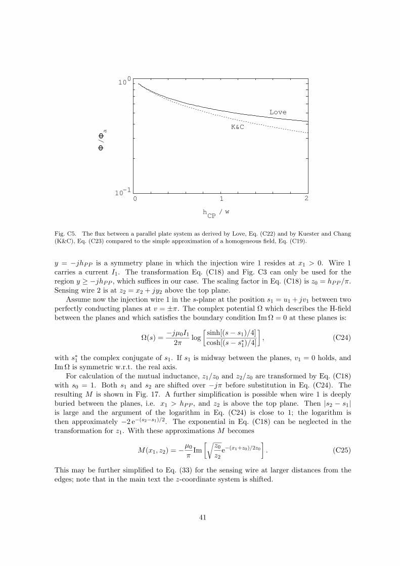
0 2
/
10-1
100
Φa
/Φ
hCP
1
Love
K&C
w
Fig. C5. The flux between a parallel plate system as derived by Love, Eq. (C22) and by Kuester and Chang(K&C), Eq. (C23) compared to the simple approximation of a homogeneous field, Eq. (C19).
y = −jhPP is a symmetry plane in which the injection wire 1 resides at x1 > 0. Wire 1carries a current I1. The transformation Eq. (C18) and Fig. C3 can only be used for theregion y ≥ −jhPP , which suffices in our case. The scaling factor in Eq. (C18) is z0 = hPP /π.Sensing wire 2 is at z2 = x2 + jy2 above the top plane.
Assume now the injection wire 1 in the s-plane at the position s1 = u1 + jv1 between twoperfectly conducting planes at v = ±π. The complex potential Ω which describes the H-fieldbetween the planes and which satisfies the boundary condition Im Ω = 0 at these planes is:
Ω(s) =−jµ0I1
2πlog
[sinh[(s− s1)/4]cosh[(s− s∗1)/4]
], (C24)
with s∗1 the complex conjugate of s1. If s1 is midway between the planes, v1 = 0 holds, andImΩ is symmetric w.r.t. the real axis.
For calculation of the mutual inductance, z1/z0 and z2/z0 are transformed by Eq. (C18)with s0 = 1. Both s1 and s2 are shifted over −jπ before substitution in Eq. (C24). Theresulting M is shown in Fig. 17. A further simplification is possible when wire 1 is deeplyburied between the planes, i.e. x1 > hPP , and z2 is above the top plane. Then |s2 − s1|is large and the argument of the logarithm in Eq. (C24) is close to 1; the logarithm isthen approximately −2 e−(s2−s1)/2. The exponential in Eq. (C18) can be neglected in thetransformation for z1. With these approximations M becomes
M(x1, z2) = −µ0
πIm
[√z0
z2e−(x1+z0)/2z0
]. (C25)
This may be further simplified to Eq. (33) for the sensing wire at larger distances from theedges; note that in the main text the z-coordinate system is shifted.
41

42
References
[1] Laan, P.C.T. van der and M.A. van Houten, A.P.J. van DeursenGrounding philosophy.In: Electromagnetic compatibility 1987. Proc. 7th International Zurich symposium andtechnical exhibition on electromagnetic compatibility. Zurich, 3-5 March 1987. Ed. by T.Dvorak. Zurich: ETH Zentrum, 1987. P. 567-572.
[2] Bergervoet, J.R.EMC measurements and models connecting the system level with the module level.Philips J. Res., Vol. 48 (1994), No’s 1-2, p. 63-81.
[3] Gravelle, L.B. and P.F. WilsonEMI/EMC in printed circuit boards: A literature review.IEEE Trans. Electromagn. Compat., Vol. EMC-34 (1992), No. 2, p. 109-116.
[4] Djordjevic, A.R. and T. K. SarkarClosed-form formulas for frequency-dependent resistance and inductance per unit lengthof microstrip and strip transmission lines.IEEE Trans. Microwave Theory Tech., Vol. MTT-42 (1994), No. 2, p. 241-8.
[5] Cerri, G. and R. De Leo, V. Mariani Primiani, A. SchiavoniInvestigation of ground plane current distribution.In: Electromagnetic compatibility 1993. Proc. 10th International Zurich symposium andtechnical exhibition on electromagnetic compatibility. Zurich, 9-11 March 1993. Zurich:ETH Zentrum, 1993. P. 195-200.
[6] Swainson, A.J.G.Radiated emission, susceptibility and crosstalk control on ground plane printed circuitboards.In: 7th Int. Conference on electromagnetic compatibility. York, 28-31 August 1990. Lon-don: IEE, 1990. P. 37-41.
[7] Ramo, S. and J.R. Whinnery, T. Van DuzerFields and waves in communication electronics. 3rd ed.New York: Wiley, 1994.
[8] Laan, P.C.T. van der and W.J.L. Jansen, E.F. SteenisDesign of shielded enclosures, in particular for high-voltage laboratories.Kema Sci. Tech. Rep., Vol. 2 (1984), No. 11, p. 101-111.
[9] Kaden, H.Wirbelstrome und Schirmung in der Nachrichtentechnik. 2nd ed.Berlin: Springer, 1959.
[10] Love, A.E.H.Some electrostatic distributions in two dimensions.Proc. London Math. Soc., Ser. 2, Vol. 22 (1923), No. 1460, p. 337-369.
43

[11] Schelkunoff, S.A.The electromagnetic theory of coaxial transmission lines and cylindrical sheets.Bell Syst. Tech. J., Vol. 13 (1934), p. 532-579.
[12] Lipinski, W. and M. Gramz, P. KrasonEin Beitrag zur Berechnung der Stromverdrangung in einem Bandleiter.Arch. Elektrotech., Vol. 62 (1980), p. 51-55.
[13] Carson, J.R.Wave propagation in overhead wires with ground return.Bell Syst. Tech. J., Vol. 5 (1926), p. 539-554.
[14] Olsen, R.G.Electromagnetic characteristics of horizontal and vertical wires above a dissipative earth.Ph. D. thesis University of Colorado, 1974.
[15] Wedepohl L.M. and A.E. EfthymiadisWave propagation in transmission lines over lossy ground: A new complete field solution.Proc. Inst. Electr. Eng., Vol. 125 (1978), No. 6, p. 505-510.
[16] Efthymiadis A.E. and L.M. WedepohlPropagation characteristics of infinitely-long single-conductor lines by the complete fieldsolution method.Proc. Inst. Electr. Eng., Vol. 125 (1978), No. 6, p. 511-517.
[17] Olyslager F. and D. De ZutterHigh-frequency transmission line models for a thin wire above a conducting ground.IEEE Trans. Electromagn. Compat., Vol. EMC-37 (1995), No. 2, p. 234-240, and refer-ences therein.
[18] Wise, W.H.Effect of ground permeability on ground return conductors.Bell Syst. Tech. J., Vol. 10 (1931), p. 472-484.
[19] Abramowitz M. and I.A. Stegun, Eds.Handbook of mathematical functions. 9th printing.New York: Dover, 1970.
[20] Harrington, R.F.Field computations by moment methods.New York: IEEE, 1993.
[21] Jaswon M.A. and G.T. SymmIntegral equation methods in potential theory and elastostatics.London: Academic press, 1977.
[22] Helvoort, M.J.A.M. vanGrounding structures for the EMC-protection of cabling and wiring.Ph.D. thesis Eindhoven University of Technology, 1995.
44

[23] Langton, N.H.The parallel-plate capacitor with symmetrical placed unequal plates.J. Electrost., Vol. 9 (1981), p. 289-305.
[24] Lin, W.Computation of the parallel-plate capacitor with symmetrical placed unequal plates.IEEE Trans. Microwave Theory Tech., Vol. MTT-33 (1985), No. 9, p. 800-807.
[25] Kuester E.F. and D. C. ChangClosed-form expressions for the current or charge distribution on parallel strips or mi-crostrips.IEEE Trans. Microwave Theory Tech., Vol. MTT-28 (1980), No. 3, p. 254-259.
[26] Gradshteyn I.S. and I.M. RyzhikTable of integrals, series and products.New York: Academic Press, 1967.
[27] Houten M.A. van and E.J.M. van Heesch, A.P.J. van Deursen, R.G. Noij, J.N.A.M. vanRooy, P.C.T. van der LaanGeneral methods for the protection of electronic equipment against interference, tested inhigh-voltage substations.In: Electromagnetic compatibility 1989. Proc. 8th International Zurich symposium andtechnical exhibition on electromagnetic compatibility. Zurich, 7-9 March 1989. Ed. by T.Dvorak. Zurich: ETH Zentrum, 1989. P. 429-434.
[28] Helvoort, M.J.A.M. van and A.P.J. van Deursen, P.C.T. van der LaanThe transfer impedance of cables with a nearby return conductor and a noncentral innerconductor.IEEE Trans. Electromagn. Compat., Vol. EMC-37 (1995), No. 2, p. 301-306.
[29] Ott, H.W.Controlling EMI by printed wiring board layout.In: Electromagnetic compatibility 1985. Proc. 6th International Zurich symposium andtechnical exhibition on electromagnetic compatibility. Zurich, 5-7 March 1985. Ed. by T.Dvorak. Zurich: ETH Zentrum, 1985. P. 127-132.
[30] Goedbloed, J.Electromagnetic compatibility.London: Prentice Hall, 1992.
[31] Bersier R. and B. SzentkutiRational and new experimental evidence on the adequacy of conducted instead of radiatedsusceptibility tests.In: Electromagnetic compatibility 1983. Proc. 5th International Zurich symposium andtechnical exhibition on electromagnetic compatibility. Zurich, 8-10 March 1983. Ed. byT. Dvorak. Zurich: ETH Zentrum, 1983. P. 257-262.
[32] Bergervoet, J.R., private communication.
45

[33] Butler C.M. and D.R. WiltonGeneral analysis of narrow strip and slots.IEEE Trans. Antennas Propagat., Vol. AP-28 (1980), No. 1, p. 42-48.
[34] Kreyszig, E.Introductory functional analysis with applications.New York: Wiley, 1978.
[35] Stakgold, I.Green’s functions and boundary value problems.New York: Wiley, 1979.
[36] Porter D. and D.S.G. StirlingIntegral equations: A practical treatment, from spectral theory to applications.New York: Cambridge University Press, 1990.
[37] Kober, H.Dictionary of Conformal Representations. 2nd ed.New York: Dover, 1957.
46