creation and annealing of point defects in germanium
TRANSCRIPT

Creation and annealing of point defects in
germanium crystal lattices by subthreshold
energy events
Sergio M. M. Coelho1, Juan F. R. Archilla2 and F. Danie Auret1
1Physics Department, University of Pretoria, South Africa2 Group of Nonlinear Physics, University of Sevilla, Spain
University of Sevilla 2013

Our team in Pretoria
Juan FR Archilla (Project leader)Group of Nonlinear Physics Lineal (GFNL)
University of Sevilla, Spain
With Sergio Coelho, F Danie Auret
Department of Physics
University of Pretoria, South Africa
Vladimir Dubinko
Kharkov Physical-Technical Institute,
Kharkov, Ukraine
Vladimir Hizhnyakov
Institute of Physics, University of Tartu
Tartu, Estonia
[email protected] Sevilla, 2013 Slide 1

[email protected] Sevilla, 2013 Slide 2
Outline
Why study this? Low energy? Really?
Germanium – ultrapure material
Hydrogen in germanium
DLTS – Deep Level Transient Spectroscopy
An experiment: ICP annealing of E-center
Summary and conclusions

[email protected] Sevilla, 2013 Slide 3
Why low energy?
Why study this? Low energy? Really?
Impacts generate Moving Intrinsic Localized
Modes (ILMs) or Discrete Breathers (DBs) in Ge
ILMs in Ge – Defect annealing 2600 nm deep
Very efficient process – Technology applications
Transferable to other systems
[email protected] Sevilla, 2013 Slide 4
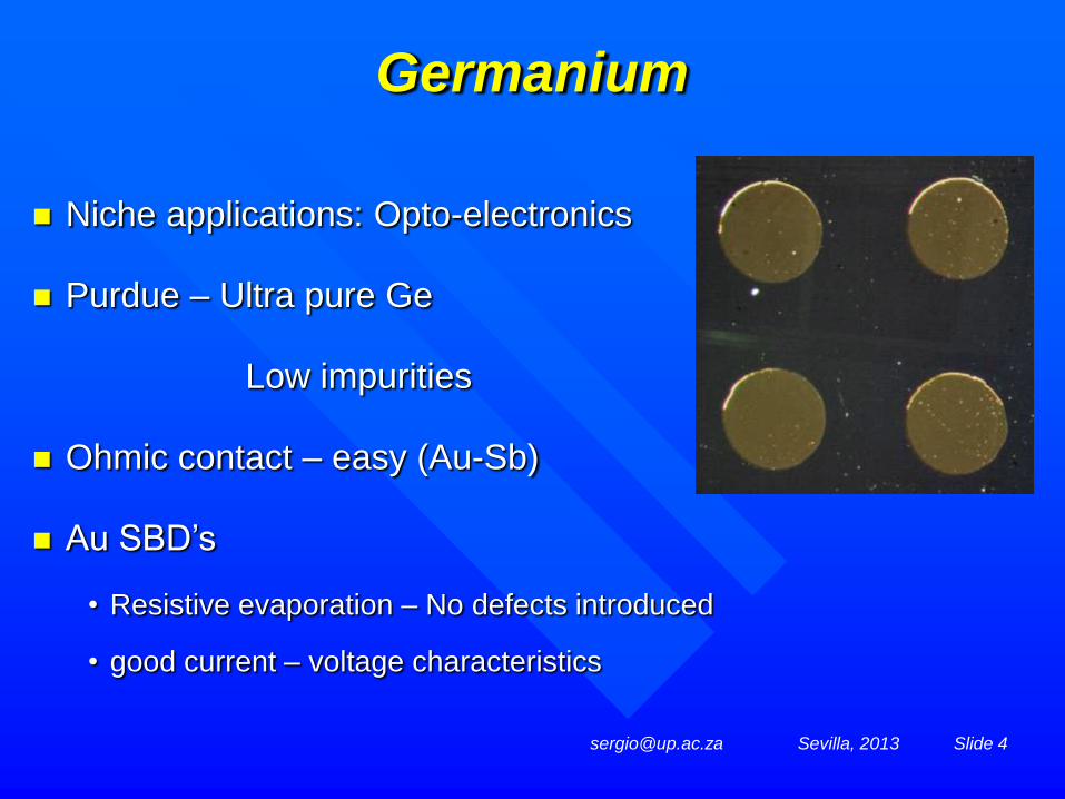
Germanium
Niche applications: Opto-electronics
Purdue – Ultra pure Ge
Low impurities
Ohmic contact – easy (Au-Sb)
Au SBD’s
• Resistive evaporation – No defects introduced
• good current – voltage characteristics
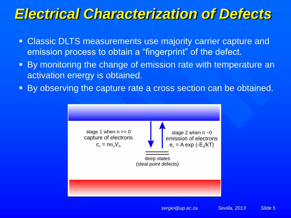
Electrical Characterization of Defects
stage 2 when n ~0
emission of electronse = A exp (-E /kT)n a
deep states(ideal point defects)
stage 1 when n >> 0
capture of electrons
c = n Vn n th
Classic DLTS measurements use majority carrier capture and
emission process to obtain a “fingerprint” of the defect.
By monitoring the change of emission rate with temperature an
activation energy is obtained.
By observing the capture rate a cross section can be obtained.
[email protected] Sevilla, 2013 Slide 5

Monitor transient as
function of temperature,T
Plot S = C(t1) – C(t2) vs T
DLTS peak
More than one level
DLTS spectrum
At the maximum of a peak:
The DLTS Spectrum1
21
21max
)ln(e
tt
tt
Typical rates: 0.1 - 1000 /s
1 D. V. Lang, JAP 45, 2023 (1974) or Schroder, ”Semiconductor Material and Device Characterization”

Deep Level Transient Spectroscopy DLTS requires a depletion (space
charge) region• p-n, metal-semiconductor, MOS, …..
Apply zero / forward bias – reverse
bias pulse sequence• Monitor C-t, I-t, … as function of T.
• Transient behaviour indicates the
Presence of defects with levels
in the band gap
Analysis of transient yields:• Distiction between majority and
minority carrier defects
• Activation enthalpy (level
position), ET
• Capture cross section,
• Defect concentration, NT(x)
• Electric field: defect type (donor,
acceptor, …)
• Uniaxial stress: defect orientation and
symmetry
Temperature (K)
0 100 200 300 400
DLT
S S
ignal:
C/C
(x10
-3)
0
1
2
3
E0
E 1E3
E1
460 Hz
46 Hz
E 2
E4
0.1 Hz
E2
5.4 MeV -particle irradiation
As-grown ZnO
46 Hz
[email protected] Sevilla, 2013 Slide 7
[email protected] Sevilla, 2013 Slide 8
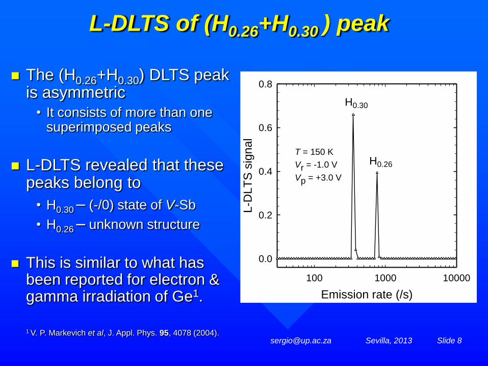
L-DLTS of (H0.26+H0.30 ) peak
The (H0.26+H0.30) DLTS peak is asymmetric
• It consists of more than one superimposed peaks
L-DLTS revealed that these peaks belong to
• H0.30 – (-/0) state of V-Sb
• H0.26 – unknown structure
This is similar to what has been reported for electron & gamma irradiation of Ge1. Emission rate (/s)
100 1000 10000
L-D
LT
S s
ignal
0.0
0.2
0.4
0.6
0.8
H0.30
H0.26
T = 150 K
Vr = -1.0 V
Vp = +3.0 V
1 V. P. Markevich et al, J. Appl. Phys. 95, 4078 (2004).

[email protected] Sevilla, 2013 Slide 9
Resistive deposition does
not introduce defects
• Curve (a)
Sputter deposition intro-
duced five electron traps1
• Curve (b)
EBD deposition intro-
duced five electron traps
• Curve (c)
DLTS: different metallization methods
Temperature (K)
0 50 100 150 200 250 300
DL
TS
Sig
na
l (p
F)
0.0
0.1
0.2
0.3
0.4
x 1
x 1
x 2
(c)
(b)
E0.38
E0.20+E0.21
E0.15
(d)
x 2
E0.13
E0.24
E0.31
x 10
x 1
x 2
ES0.14
ES0.20+ES0.21
ES0.31ES0.24
(a)
H0.30
x 10
All the SD induced defects are also
introduced by MeV electron irradiation• Curve (d)
1 F. D. Auret et al, J. Electron. Mat. 36, 1604 (2007).

DLTS: Example, two RW: Defect E center
10
)exp(
)(80
1
2
1
1
1
1
kT
ET
TesRW
Tnn
n
)exp(
)(200
2
2
2
2
1
2
kT
ET
TesRW
Tnn
n
determined be
can and Tn E

Number of traps for n-type semiconductor:
11
D
t
N
N
C
C
2
0
The number of traps Nt can be
determined
ND :concentration of
donors
The depletion layer with W
increases with the bias potential:
The profile Nt(x) can be obtained

Annealing at room temperature
12
Annealing rate constant k(T)
can be determined
Isochronal annealing: same
time, different temperatures
Annealing activation energy
E0 can be determined
tt k(T)N
dt
dN-
)exp( 0
Tk
Ek(T)
B

Sample Preparation
Sevilla, 2013 Slide 13
Chemical cleaning, ie degreasing
Chemical etch – oxide removal
RF Sputter etch – Ar ICP
Use COPRA plasma source
• Inductively coupled plasma (ICP)
• Low energy Ar ions: 1 - 120 eV
• Fluence rate: 1015 cm-2 s-1
• Etch rates: 0.1 nm s-1 for Ge
• Area: several tens of square cm

Sevilla, 2013 Slide 14
Caution
4 eV Ar ICP: Average at sample
3.7 eV transfer to Ge atom
Sample temperature increases
3 x 10 minute ICP (40°C)
Annealing also in time and at increased temperature
Sample temperature increases
3 x 10 minute ICP (40°C)
Hydrogen passivation of defects

Our basic experiment: 4 eV Ar-ICP plasma
annealing
15
1.-Sb doped Ge is damaged
with 5 MeV alpha particles
Rest – 24 hours
2.-Au diode is evaporated in
half the sample (half A)
3.- DLTS on A (black)
4.-ICP on A and B: 3 x 10 min
5.- Au RE - diode B
6.- DLTS on A (red-dashed)
7.- DLTS on B (blue)
[email protected] Sevilla, 2013 Slide 16
Observations
4 eV ICP: E-center concentration -30%
Effect depth in Ge: exceeds 2600 nm
ICP through metal – less annealing
Annealing diminished with higher sample temperature.
1 x 30 minute ICP (70°C)
8 eV Ar ICP (T ?)
Compare to anneal with phonons:
• Low T (40 °C) ~ 150 °C
• High efficiency Lower efficiency

17
Our hypothesis: Ar ions impacting on Ge produce
Intrinsic Localised Modes that travel through Ge and
anneal defects. Why?
1.-ILMs with MD in metals by Hyzhnyakov group have 0.5-5 eV
2.-The maximum energy transfer from Ar to Ge is 3.6 eV
3.- The activation energy for annealing an E center is about 1.36 eV
4.- Energy remains localized exceeding 4000 lattice units
5.- Increasing the energy of the plasma does not enhance the effect, this
is because ILMs typically have a definite range or energies.
6. Increasing sample temperature – effect diminished.
7.- At least stationary ILMs have been obtained for Si and Ge with MD.

18
Conclusions:
Plasma of 4eV produces annealing of defects very deep in
Ge.
The energy delivered to E-center is ~1 eV.
1. 4 eV Ar hit produces an ILM in Ge with very high efficiency .
2. ILM of energy ~3eV travel distances of the order of
104 lattice units or more.
3. The annealing efficiency of ILM with respect to phonons is
extremely large.
Likely conclusions:

Sevilla, 2013 Slide 19
Gracias
Acknowledgements
J. F. R. Archilla – many suggestions & hospitality
South African NRF – Financial assistance
Group members for listening & helpful comments.

Our basic experiment: Facts
20
1.-Sb concentration: 1.3·1015 cm-3 (ni= 2.4·1013 cm-3) ; 1 Sb per 108 Ge
2.- Metal (Au) thickness: 25nm
3.- After ICP on Ge the E center concentration drops 29% from NT=
1.07·1014 cm-3
4.- If ICP is done on Au, the E center reduction is smaller, but exists.
5.- ICP is done for 30’ in intervals to prevent heating
6.- Defect annealing occurs up to 2600 nm or 4600 lattice units
7.- If the plasma energy is increased the effect is smaller
8.- Thermal annealing has to be done at 150°C to obtain a similar effect.
21
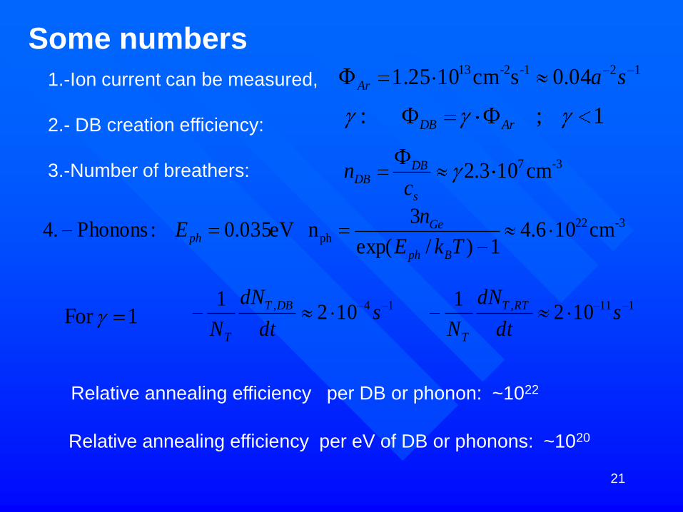
Some numbers
1.-Ion current can be measured,
2.- DB creation efficiency:
3.-Number of breathers:
12-1-213 04.0scm101.25 saAr
1 ; : ArDB
cm106.4 1)/exp(
3n eV035.0 :Phonons.4 3-22
phTkE
nE
Bph
Geph
1For 111,14, 102
1 102
1s
dt
dN
Ns
dt
dN
N
RTT
T
DBT
T
Relative annealing efficiency per DB or phonon: ~1022
Relative annealing efficiency per eV of DB or phonons: ~1020
cm103.2 3-7
s
DBDB
cn

22
Interaction cross-section and energy delivered
by a breather
)exp( 0
Tk
EN
dt
dN
B
DBTT
Interaction cross-section
Minimal interacion cross-section
Apparent diminution of the activation energy because of DB
interaction: Δ
1 ; 0
2153/2
0 сm10Gen
)exp( 00
Tk
EN
dt
dN
B
ionsTT unknown ,,
Interaction cross-section σ
217-
0 cm101.5 50
1ionsionsTions
T Ndt
dN
eV2.1 , 1For

23
References
.

[email protected] Sevilla, 2013 Slide 2
Electron beam deposition
Advantages:
• Easily evaporates high
melting point metals.
• Highly controllable
deposition rates.
• Good adhesion.
Disadvantage:
• Introduces defects at and
below the surface of
semiconductors.
• Chen et al
• Mooney et al

E vs AMU for e or H
11.5 eV to create
Frenkel pair
1st: electron-atom
2nd atom to crystal
Example: e to H to
Ge
[email protected] Sevilla, 2013 Slide 2

[email protected] Sevilla, 2013 Slide 2
The Defect Concentration
Defect concentration from peak height, C/C:1
12
p
2
0
m )(2)(x
x
x
x
C
CxNxN
t
DT
NT as low as 1010 defects /cm3
1 Y. Zohta et al, JAP. 53, 1809 (1982)
D
pm
qN
VVx
xxx
bi2
2/)(
DNq
EE2
TF )(2

[email protected] Sevilla, 2013 Slide 2
Depth Distribution of EBD defects
Use fixed bias, variable pulse
DLTS method
• With “ ” correction1.
Not possible to profile the hole
traps:
• Hole concentration is not known.
V-Sb (E0.38):
• Concentration decreases rapidly
away from the surface.
• Approaches 1014 cm-3 at surface.
• Diffusion of vacancies from the
surface?
1 Y. Zohta et al. J. Appl. Phys. 53, 1809 (1981)
Depth below junction (microns)
0.0 0.1 0.2 0.3 0.4 0.5
Defe
ct C
oncentr
ation (
cm
-3)
1012
1013
1014
E0.38
below a Pt SBD formed by EBD
Vr = -2.0 V
T = 205 KdVp = 0.1 V

[email protected] Sevilla, 2013 Slide 2
E-beam deposition - Pt
10 keV electrons
Beam path
Reflected electrons
Particles
Experiment 1

[email protected] Sevilla, 2013 Slide 2
E-beam shielding e-traps
High vacuum-2 shields
F/gas – 2 shields
F/gas – 1 shield
F/gas – no shields
“Standard EBD”

[email protected] Sevilla, 2013 Slide 2
E-beam shielding h-traps
High vacuum-2 shields
F/gas – 2 shields
F/gas – 1 shield
F/gas – no shields
“Standard EBD”
[email protected] Sevilla, 2013 Slide 2
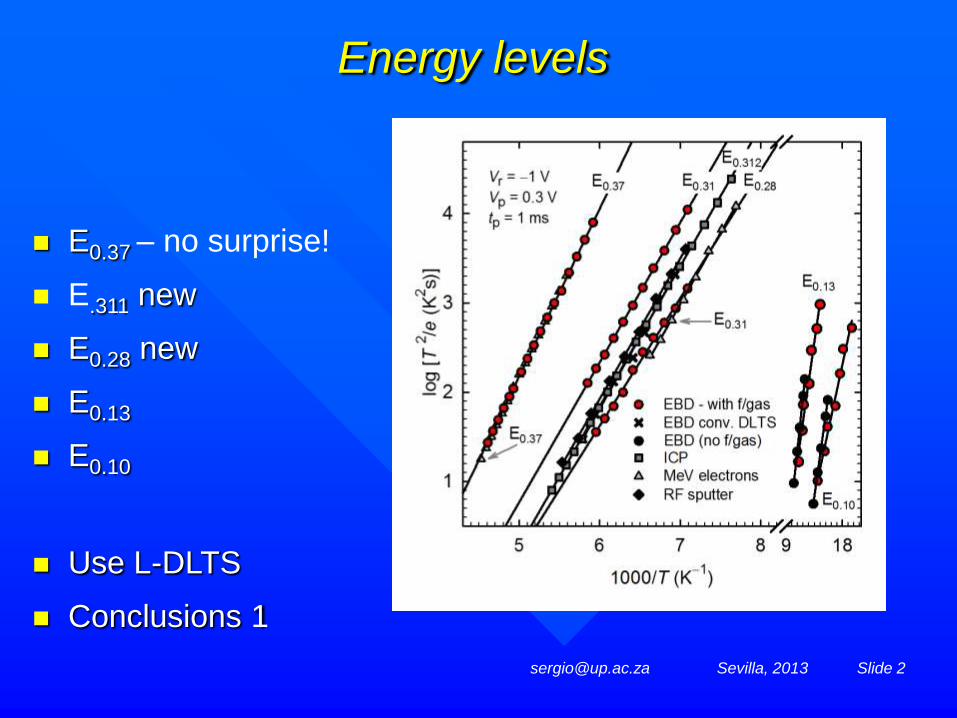
Energy levels
E0.37 – no surprise!
E.311 new
E0.28 new
E0.13
E0.10
Use L-DLTS
Conclusions 1


[email protected] Sevilla, 2013 Slide 2
Arrhenius plots – L-DLTS
No hole traps
in common
New defects –
impurity related?
[email protected] Sevilla, 2013 Slide 2
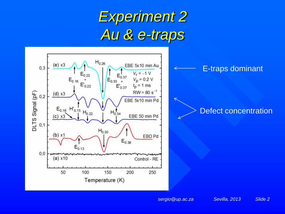
Experiment 2
Au & e-traps
Defect concentration
E-traps dominant

[email protected] Sevilla, 2013 Slide 2
Arrhenius plots – L-DLTS
E0.38
Common to both
New defects – perhaps
not impurity related
[email protected] Sevilla, 2013 Slide 2
Summary and Conclusions
1. Shielding lowers the defects introduced by EBD.
Damage caused by impacts with ions / particles – not e.
2. Damage caused in 1st 0.5 µm, at / near defect site.
How was the energy transferred?
3. Damage caused by E < 1.3 eV transfer to Ge.
Only enough to displace H or light atoms – single bond.
Will DLTS be more useful in future?

[email protected] Sevilla, 2013 Slide 2
Thank you
Acknowledgements
J. F. R. Archilla – many suggestions & hospitality
South African NRF – Financial assistance
Group members for listening & helpful comments.

[email protected] Sevilla, 2013 Slide 2
MeV electrons
Temperature (K)
0 50 100 150 200 250 300
DLT
S S
ignal (p
F)
0.0
0.5
1.0
x 10
x10
E0.31
E0.37
(b)
x 1
x 1
E0.10
(c)
E0.25+E0.31
E0.24
E0.21
E0.20 E0.15
x5
E0.24
(d)
x 10
(a)
Vr = 2 V
VP = 0 V
tp = 1 ms
RW = 80 s1
E0.31 E? E?
MeV electrons
Alpha irradiation
RF sputter etch

[email protected] Sevilla, 2013 Slide 2
Electron beam deposition
H0.15
Fig. 7 (of 7 ), S. M. M. Coelho et al
*
*
*
*
Emission rate (s-1
)
1 10 100 1000
L-D
LT
S s
ignal
0.000
0.004
0.008
0.012108 K
105 K
102 K
99 K
Vr = -1 V
VP = 3 V
tp = 1 ms
* H0.22
H0.225

E vs AMU for e or H
11.5 eV to
create
Frenkel pair
[email protected] Sevilla, 2013 Slide 2
Atomic mass (AMU)
0 10 20 30 40 50
Energ
y (
eV
)
0
5
10
15
20
25
10 keV electrons24eV hydrogen

[email protected] Sevilla, 2013 Slide 2
I-V: Pt diodes
Voltage (V)
0.0 0.2 0.4 0.6 0.8 1.0
Cu
rre
nt
(A)
10-7
10-6
10-5
10-4
10-3
10-2
Reverse bias
Forward bias
No shields with forming gas
2 shields & high vacuum
No shield Standard vacuum
Ideality = 1.02
Previous lowest: 1.05
Current – lowest measured
Defects linked to e-beam
Next experiment

Defects in Semiconductors
Defects can be “good” or “bad”
• Solar cells: “bad”: eliminate them!!!
• Fast switches: “good”: deliberately introduce them!
Defects are introduced during
• Crystal growth, sawing / cutting and polishing
• Critical processing steps» Surface cleaning by particle processing (sputter etching)
» Metallization
• Radiation» Space, reactors
» Accelerators / implanters
Important defect parameters
• Energy level, ET, in bandgap
• Capture cross section,
• Concentration, NT
[email protected] Sevilla, 2013 Slide 2