crystal growth laboratory · crystal growth laboratory ... deposition of sic • thin films of...
TRANSCRIPT

http://www.cgl-erlangen.com
Crystal Growth Laboratory
Your Competent Partner in Crystal Growth and Solidification Processes
Annual Report 2006
- Equipment and Process Development - - Optical and Electrical Characterization -
- Numerical Modeling -


Content
contact: [email protected]
Structure Overview Research Fields
Properties of LPSG GaN substrates Analysis of the kinetics of the formation of precipitates in multi-crystalline silicon for solar cells CrysMAS – a new simulation tool for global modeling of crystal growth processes Modeling of melt convection during ingot casting of silicon for solar cells Multi-scale modeling of the microstructure formation during the directional solidification of alloys
Equipment Publications Contact

Structure
Crystal Growth Laboratory
Epitaxy/Layer deposition • Low pressure solution
growth of GaN • Chemical Vapor
Deposition of SiC • Thin films of chalcopyrite
(CIS)
Melt growth • Directionally solidified
solar silicon • Solar silicon tubes • Low defect compound
semiconductors • Perfect CaF2 crystals • Sapphire ribbons
Modeling • Process and defect
models • 3D simulation • Bulk growth processes • Crystal growth facilities • Alloy solidification • Licensing of software
Defect engineering • Defects in SiC epitaxial
layers • Precipitates in
multicrystalline silicon • Dislocations in GaN and
other compound semiconductors

Overview
contact: [email protected]
Crystal growth processes provide basic materials for many applications. The research and development of crystal growth processes is driven by the demands which come from the specific applications; but in general there is a need for an increase of crystal dimensions, improved uniformity of the relevant crystal properties in the micro and macroscale and materials with new properties. Therefore, the focal area of research of the Crystal Growth Laboratory (CGL) is to develop – in close collaboration with industry - equipment and processes for the production of bulk crystals and thin films in order to meet the increasing requirements on crystal quality and cost reduction. The strategy of CGL is to optimize the crystal growth processing by a combined use of experimental process analysis and computer modeling. These activities are
based on a suitable experimental infrastructure and on highly efficient user friendly simulation programs named CrysVUn, CrysMAS3D and STHAMAS3D. These computer codes, which are continuously further developed, are used for and by the industrial partners to develop crystal growth equipment and processes. CGL was founded at the Department of Materials Science of the University of Erlangen - Nuremberg by Prof. Dr. Georg Mueller in 1979. Since 1996 the Crystal Growth Laboratory has established the working group "Crystal Growth" at the Fraunhofer Institute for Integrated Systems and Device Technology (IISB) in Erlangen. This working group became the Department Crystal Growth in autumn 1999. Since 2005 the CGL is also present in Freiberg/Saxonia within the Fraunhofer Technology Center for Semiconductors which is a common subsidiary of Fraunhofer IISB from Erlangen
and Fraunhofer ISE from Freiburg. Since the foundation of CGL more than 250 papers in scientific journals and conference proceedings have been published. Furthermore, CGL has educated a lot of experts in this field. Around 200 "Study" and diploma theses and around 40 PhD theses may serve as a reference for this. More than 90% of funding of the Department of Crystal Growth result from research contracts directly with industrial partners or with public funding organizations like the Federal Ministry for Education and Research, the Bavarian Research Foundation. Since 1996, CGL has acquired almost 20 Mio. Euro from the different sources indicated above. Today, CGL consists of around 35 highly motivated coworkers. They are experts in different fields, like systems engineering, metrology, computer simulation,
Fig. 1: Participants of the 5th International Workshop on Modeling in Crystal Growth
(IMWCG-5), September 10 to13, 2006, Bamberg, Germany IWMCG-5 was organized by CGL.

Overview
contact: [email protected]
physics, material science, mathematics. In 2006 the Crystal Growth Laboratory has consolidated its position as word-wide acknowledged center of competence in the field of crystal growth. In the field of manufacturing of GaN-substrates from metallic solutions under ambient pressure conditions a theoretical model was developed which can explain the experimentally observed reduction of the dislocation density in the solution grown GaN by a factor 10 to 100. Thereby, the occurrence of growth islands with facets at the beginning of the growth process is important for the reduction of the dislocation density. Furthermore, the partner Fraunhofer IAF from Freiburg has for the first time successfully produced lightning LED test structure on as grown and polished surfaces of GaN-templates delivered by CGL. In addition, CGL has demonstrated the first solution grown GaN with 3” diameter.
The start of the operational business in the new subsidiary of Fraunhofer IISB, the technology centre for semiconductor materials in Freiberg, strengthens the collaboration of CGL with the local industrial partners. Thereby, especially in the area of directional solidification of solar silicon first important contributions were obtained about a better understanding of the heat and mass transport phenomena occurring during the growth process. These contributions help to explain the experimental observations. In the area of the manufacturing of high melting oxide crystals a basic process for the growth of sapphire ribbons was developed after the successful commissioning of a new crystal growth puller. This process development was possible only due to a grant funded by the Bavarian Science Foundation. In the field of modeling the software CrysMAS, which is the main product of CGL, was tailored further in order fulfill the needs of the customers with respect to easier usage and
more efficient computation of fluid problems. It is possible with the present software to treat the melt convection in a local three-dimensional model within a global axi-symmetric thermal simulation of the whole crystal growth facility. The local model is completely integrated in the global model without the need to change the software or to exchange data to an external program. Last but not least several invited talks during international conferences as well as the collaboration in different national and international expert panels in the field of crystal growth have contributed to strengthen the international reputation of CGL. Furthermore, CGL has organized several events. At this point it has to be mentioned especially the 5th International Workshop on Modeling in Crystal Growth which is the largest conference on this topic. CGL works closely with research institutions and maintains national but also international co-operations to industry.
Fig. 2: CGL has initiated a collaboration with the Gymnasium Eckental. In this collaboration CGL is
advising young scholars doing experiments in crystal growth and characterization. The collaboration is supported by the German Association of Crystal growth (DGKK).

Properties of LPSG GaN substrates
contact: [email protected]
GaN substrates with low dislocation density can significantly enhance the performance of GaN based devices (LED, transistors) or the availability of low dislocation substrates is essential at all like in the case of laser diodes. Despite the high research activity it is still difficult to produce low defect substrates which are cut from a massive GaN crystal. With respect to the production of a volume crystal the GaN system is extraordinarily difficult. Many fundamental questions of the classical crystal growth, like growth kinetics or nucleation processes, are not answered for this particular material system. Due to that fact a single crystal with a diameter of 50 mm and several centimeters in length, does still not seem to be lying ahead for the near or medial future. With the so-called GaN templates there is indeed an
attractive material available, suitable for industrial application. The GaN templates offer a low dislocation GaN layer on top of a foreign substrate, which can be used for homoepitaxial like device processes. The GaN layers produced at CGL, after the low pressure solution growth process (LPSG), are such a template solution. Figure 1 shows a template with a 2" diameter. This material represents a template with a LPSG GaN layer grown on a sapphire substrate with a seeding layer. The LPSG GaN has about one to two orders of magnitude lower dislocation density compared to conventional material deposited from the gas phase. An intensified recombination process takes place, already within the first micrometer of growth after the seed interface, due to the bending off of dislocations from the main growth direction. This behavior can be explained by the growth mode of the layer during the
initial growth. Special crystal facets are developed during the initial growth period. These growth facets can attract a dislocation to bend to the facet and move into another slip system, which will lower the total energy of the dislocation. This energy minimization is considered to be the driving force for the bending of the dislocations. As a result of the bending, the probability for the reaction between dislocations is enhanced and in case of opposite burgers vectors, dislocations can annihilate, which will result in a reduced dislocation density (Figure 2). The structural properties of GaN templates are of particular importance, since life time and performance of devices depend strongly on the quality of the substrate used. A better understanding of the growth process and the resulting materials properties are therefore in the centre of the actual research work. We managed to optimize the
Fig. 1: LPSG-GaN template grown on sapphire with 2" diameter.

Properties of LPSG GaN substrates
contact: [email protected]
solution growth process, such that the density of macro defects was remarkably reduced. The better control of the supersaturation during the growth of the layers leads to a minimization of unwanted parasitic GaN crystallite formation. However, the as-grown surfaces of the GaN layers are usually defined by hexagonal hillocks, which can have up to 100µm in diameter. For an application of this type of material in an epitaxial process those surface structures must be planarized, as long as the formation of the hillocks can not be avoided during the growth
process. For GaN there are yet no optimized polishing processes available which allow to produce epi-ready surfaces without the typical so-called subsurface damage induced by the preparation process. With again better adjusted growth conditions it was possible to produce as grown surfaces with a surface morphology which made it possible to fabricate LED test structures directly on the as-grown LPSG GaN surfaces without an additional preparation step. For all the tested LPSG materials an electroluminescence was measured. Although the
luminescence intensities measured were still smaller compared to conventional optimized LED structures on MOCVD material, there is a wide range for possible optimization of the LPSG GaN material as well as the the surface quality and the following epitaxial process. The further development of the LPSG material and the epitaxy procedure is done in close collaboration with the Faunhofer IAF at Freiburg. The work is carried out within the project 01BM580 funded by the Federal Ministry for Education and Research
Fig. 2: Bending, reaction and annihilation of dislocations at the interface between the MOCVD seed
layer and the LPSG GaN layer, TEM image.

Analysis of the kinetics of the formation of precipitates in multi-crystalline silicon for solar cells
contact: [email protected]
Photovoltaic is one of the economic branches, which has grown significantly in the last few years. This growth has a direct impact on the creation of new jobs, on the reduction of the CO2-output, on the increase of renewable energies and on the protection of the environment and resources. Currently, the bottleneck of the availability of the silicon feedstock becomes one of the important problems in photovoltaic industry. It is anticipated that this deficit of raw material will prevail at least until 2007/2008. Therefore, much more efficient methods for manufacturing of silicon wafers are required. Once this shortage of the silicon feedstock is handled efficiently, the demand for silicon wafers can quantitatively be met easily, for the production of solar cells. However, the material quality of the silicon wafers will decide
the ranking of the manufacturers in comparison to their competitors. The necessary silicon material for solar cells is manufactured by the principle of directional solidification. A silicon block is produced from the feedstock material by a melting and crystallization process. After separating the block into columns the individual silicon wafers are produced by wire sawing. The quality of the silicon wafers is extremely dependent on the heat- and mass transport occurring during the crystallization and cooling process. Despite of the very well known fact that melt convection plays an important role for the heat and mass transport, the basic understanding about its mechanism and consequences to the properties of the silicon
wafer is lacking. The heat- and mass transport phenomena are essential for the appearance of the defects in silicon, like stress, dislocations, metallic impurities and in particular also inclusions or precipitates (SiO2, SiC, Si3N4). These defects can reduce the charge carrier lifetime in the silicon wafer and lead to a lower efficiency of the solar cells. In addition, the precipitates can be responsible for short circuits in the solar cell and might trigger a total breakdown of the energy conversion. Early this year the Technology Centre for Semiconductor Materials (THM) Freiberg started a close collaboration together with an industrial partner within the framework of the KoWäSto Project (P11096) in order to improve the material quality for silicon wafers. THM
Fig. 1 grain boundaries (1), twin lamellae (2), etchpits, in polycrystalline silicon,
visualised by etching after Wright-Jenkins-Etch

Analysis of the kinetics of the formation of precipitates in multi-crystalline silicon for solar cells
contact: [email protected]
is a combined branch of Fraunhofer IISB, Erlangen and Fraunhofer ISE, Freiburg. Unlike normal industrial furnaces we have developed a special R&D furnace to vary individual process parameters very easily, to check the influence on the material quality. By means of different etching methods, grain boundaries and defects could be visualized on the surface of the polycrystalline silicon material. These defects are possible recombination centers for charge carriers. Silicon is transparent in the infrared spectral zone, therefore individual precipitates appear as dark contrasts in an infrared
transmitted light photograph in the silicon crystal. These precipitates can be crystallographically and chemically analyzed after they have dissolved from the silicon matrix. By means of a scanning electron microscope (SEM) it is possible to make a high resolution picture of the morphology of the precipitates. The energy dispersive X-ray (EDX) allows it to gather information about the chemical composition of the precipitates. With the aid of these methods, the existence of SiC and Si3N4 precipitates can be proved in the inner core of the silicon matrix. The observation shows that the
interior parts of the crystallization furnace (insulating materials, crucible materials, crucible coating, and atmosphere) have a considerable influence on the creation of The current research activities are concentrated on the individual growing mechanism for the different precipitates. The aim of this work is to limit the occurrence of the precipitates and to reduce or even to eliminate them totally. The research and development activities are funded partly by the European Regional Development Fund 2000-2006 (ERDF) and by the ministry of economics and employment of the state of Saxony.
Fig. 2: SEM picture of the precipitates, which are dissolved from the Si matrix. With the arrow marked (1)
Si3N4-rod (2) SiC-cluster which grows form the (1) (3) SiC filaments which grows from the (2)

CrysMAS: a new simulation tool for global modeling of crystal growth processes
contact: [email protected]
Modeling of convective phenomena in crystal growth configurations is still quite challenging. Today the standard engineering way of modeling uses a quasi-stationary and axisymmetric, i.e. 2D global model of the whole crystal growth facility. Thereby, it has been shown that the block-structured meshes are very effective for convection dominated problems which occur for example in the Czochralski process. However, the disadvantage of such software is the conditional degree of automation of the preprocessing and the decreasing convergence rate for very complex geometries. On the other hand, software which is based on an unstructured triangulated mesh has been proven to be very
powerful in terms of automation of the preprocessing and in terms of solving inverse problems, but less efficient for the treatment of convective phenomena. Recently, a new category of software, named CrysMAS, was developed which uses a combination of block-structured and unstructured mesh, a so-called a hybrid mesh, in order to benefit from the advantages of both schemas. The concept of the hybrid software CrysMAS was described earlier. A high numerical efficiency was already achieved for modeling of various crystal growth methods like Czochralski, Bridgman, EFG in the framework of this concept especially concerning the nonlinear processes like the
buoyancy driven convection. The next target for the model development was the expansion of the global 2D model towards a local 3D model of the melt flow which is fully thermally coupled with 2D model. The 3D model must be completely incorporated into the available code CrysMAS. The fluid dynamics formulation is done in cylindrical coordinates. Thereby, the radial and axial coordinates are identical with the one in the global 2D model. This simplifies the data exchange by the thermal coupling and the 3D data structures. The 3D fluid dynamics model was verified on the basis of test cases for the GaAs melt flow in a tilted Bridgman configuration (see figure 1). The next important issue is the
Fig. 1: Profile of the axial flow velocity at the symmetry axis computed for a GaAs melt cylinder for
different computer programs. The number of CVs was 257 600 (100x28x92) for STHAMAS3D coarse, 546 000 (130 x 35 x 120) for STHAMAS3D fine, ~ 5 000 for CrysVUn, ~ 20 000 for CrysMAS2D and
108x46x53 (z x r x φ) for CrysMAS3D.

CrysMAS: a new simulation tool for global modeling of crystal growth processes
contact: [email protected]
managing of the thermal coupling between the local 3D and the global 2D models. The thermal back coupling is essential for a realistic modeling of the Cz melt flow, because the melt flow changes the heat resistivity of the melt and affects therefore the boundary temperature on the crucible wall. The classical approach is the data exchange along the shared boundary. Thereby, the boundary conditions are set using the boundary data of the external model. The area of the local 3D model is then cut of from the global 2D model and not considered during the 2D computational run. In addition to the classical coupling scheme a new concept is suggested and implemented which is based on the following.
The temporally and azimuthally averaged convective mass fluxes and turbulent heat fluxes inside of the melt are evaluated during the 3D run and transferred to 2D according to this concept. The 2D solution based on the averaged data corresponds to the Reynolds' averaged enthalpy equation. A quasi stationary state solution for the 2D temporally averaged heat transfer and crystal geometry is looking for. Both concepts of coupling were applied for various Cz melt flows and their efficiency was compared. A typical instantaneous velocity distribution in the melt is shown in Fig. 2. The test cases for GaAs and coupling according to the Reynolds' averaging have indicated the required real time
in 3D to be above 500 seconds for an evaluation of the turbulent heat fluxes. The required time was strongly reduced by the application of the same coupling scheme for a Si Cz melt flow. The time reduction might be explained by the lower value of the Prandtl number and therefore the slighter influence of the turbulent heat fluxes. The data exchange along the shared wall and the time dependent solution for both 2D and 3D domains will be preferred in the future coupling scheme. The work is partly funded by Freiberger Compound Materials and Schott Solar.
Fig. 2: The instantaneous state of the 3D time dependent GaAs melt flow in the Cz 6'' configuration. The
hot zone is shown consisting of crystal, melt, crucible, heater and graphite components. The distribution of the axial velocity component by isolines and color coded polygons in two azimuthal and one horizontal
cross-section under the crystal is shown. The result was computed by means of the numerical code CrysMAS in the fully thermally coupled mode with the global model. Melt and crucible were simulated in
3D, the other compounds in 2D.

Modeling of melt convection during ingot casting of solar silicon
contact: [email protected]
Directional solidification of multi-crystalline Silicon is the industrial production technique with the largest market share for solar Silicon of about 60%. Today, Silicon ingots with a weight of over 300kg are produced by directional solidification methods. In order to support the process development and to improve the understanding of the heat and mass transport phenomena occurring during the crystallization process numerical modeling is applied. In previous investigations of the heat transport during directional solidification of solar Silicon, melt convection was often neglected. However, due to the
large dimensions of the melt container it seems to be necessary to consider also the influence of melt convection on the heat and species transport during directional solidification. The origin of convective flows in directional solidification of solar Silicon, which is a so-called “hydrodynamically stable” growth configurations with temperatures increasing from bottom to top, are radial temperature gradients which are leading to a bending of the solid-liquid interface and thus to buoyant convection. We concentrate on the study of the influence of convective flows on the casting process of
solar Silicon in order to get some basic understanding of the role of convection. A simplified three-dimensional model of an industrial directional solidification process of Silicon in a mould is used. The influence of various growth parameters (size of the mould, crystallization rate, etc.) is studied by numerical simulation using the program STHAMAS3D. A simplified geometry, consisting only of melt and already solidified Silicon is being used. Temperature boundary conditions obtained from measurements are applied on the boundaries The mesh in the melt consists typically of 380.000 control volumes (CV),
Fig. 1: Velocity field in a horizontal section placed 2 cm under the free surface (top) and in a vertical
section placed in the center of the mould (bottom)
Modeling of melt convection during ingot casting of solar silicon
contact: [email protected]
which was found to be sufficient to resolve the main features of the flow. In order to obtain a realistic solution starting from an arbitrary initial solution at least 800 sec of real time should be computed with a time step of 0.1 sec. Therefore, a huge computational power is needed to perform a parametric study, even for this local model. However, due to the high performance of actual personal computers and taking advantage of parallel computing such calculations can be performed in reasonable times especially on a PC cluster. The 3D time-dependent simulations of this work were carried out on a 12 node HP-AMD-Opteron 2.2GHz cluster (1 Gbit/s switched) with the parallelized version of STHAMAS3D. With this PC cluster the time per run
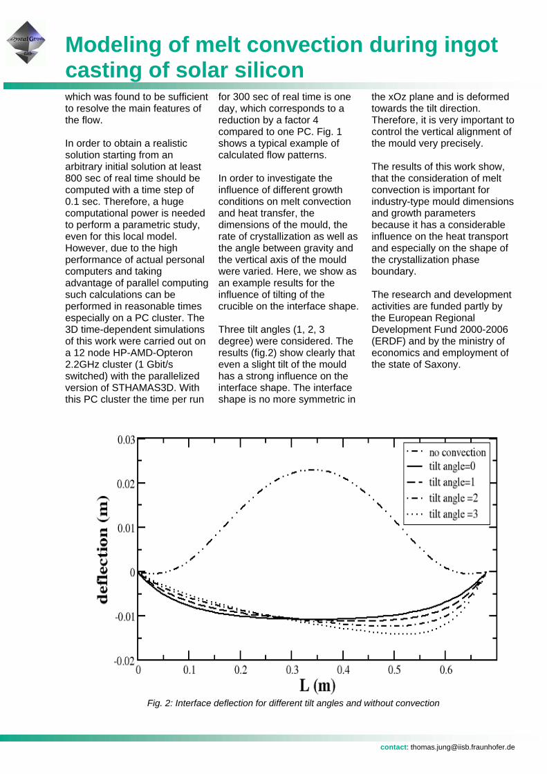
for 300 sec of real time is one day, which corresponds to a reduction by a factor 4 compared to one PC. Fig. 1 shows a typical example of calculated flow patterns. In order to investigate the influence of different growth conditions on melt convection and heat transfer, the dimensions of the mould, the rate of crystallization as well as the angle between gravity and the vertical axis of the mould were varied. Here, we show as an example results for the influence of tilting of the crucible on the interface shape. Three tilt angles (1, 2, 3 degree) were considered. The results (fig.2) show clearly that even a slight tilt of the mould has a strong influence on the interface shape. The interface shape is no more symmetric in
the xOz plane and is deformed towards the tilt direction. Therefore, it is very important to control the vertical alignment of the mould very precisely. The results of this work show, that the consideration of melt convection is important for industry-type mould dimensions and growth parameters because it has a considerable influence on the heat transport and especially on the shape of the crystallization phase boundary. The research and development activities are funded partly by the European Regional Development Fund 2000-2006 (ERDF) and by the ministry of economics and employment of the state of Saxony.
Fig. 2: Interface deflection for different tilt angles and without convection

Multi-scale modeling of the microstructure formation during the directional solidification of alloys
contact: [email protected]
Solidification processes of metallic alloys have a very high importance in industry. Almost every component made of metal had at least one process of solidification during its life cycle. Depending on its further processing all or at least some properties of the component are defined by the casting process. The physical phenomena found in the mushy zone during the solidification process are of great complexity. Technical alloys solidify usually with dendritic interface morphology as shown in figure 1. In this interface area between the melt and the fully solidified component a considerable number of phases and
structures are formed, which define the later properties of the material. For example the spacing between the primary (λ1) and the secondary (λ2) dendritic arms defines the distance between hard precipitations, which may form out of the alloy components in the melt and constitute between the arms. This distance of the particles determines the mechanical strength for many alloys. The numerical modeling of these processes would make it much easier to guaranty specific material properties of a component. To get closer to this objective CGL and European partners work
together within the framework of the MICAST project on the analysis and modeling of the microstructure formation. In these studies the so-called directional solidification method is used. This has the advantage that the formed microstructure is also directed and therefore ordered. This facilitates or in the first place enables a quantitative analysis of important parameters such as the primary dendritic arm spacing. Important parts of the project are microgravity experiments. These are necessary to eliminate the interfering buoyancy inside the sample. Some of the experiments are
Fig. 1: Decanted dendritic interface of a directionally solidified AlSi7 sample.
(Source: ACCESS –Aachen)

Multi-scale modeling of the microstructure formation during the directional solidification of alloys
contact: [email protected]
carried out with sounding rockets which provide about 15 minutes of microgravity time. These experiments are performed by the Institute of Space Simulation of the DLR in Cologne, which developed the furnaces ARTEX and ARTEX+. CGL supports this work by numerical simulation. For example thermal simulations of the complete furnace are performed. They provide a tool for testing and optimizing of the process and the furnaces. Amongst others it was
investigated if the capacity of the cooling system in the rocket was sufficient for the furnaces. With the aid of a volume averaging method the models also take the mushy zone into account. Figure 4 shows the model of the furnace ARTEX+. The models also allow detailed calculations of the microstructures in the specimen, which is mainly characterized by the primary and the secondary dendritic arm spacing. Because these
calculations include the temperature distribution in the furnace, it is possible to directly compare the computed and measured microstructure properties, which makes a validation of the models for further application easier. The work is financially supported by DLR (project 50WM0546) and by ESA (ESA MAP project 1437-00-NL-SH) with in MICAST III.
Fig. 2: Global thermal model of the ARTEX+ facility. The right half shows the temperature field, the left one
the numerical grid.

Publications
2006 G. Sun, E. Meissner, S. Hussy, B. Birkmann, J. Friedrich and G. Müller Morphologies of GaN single crystals grown from Ga solutions under flowing ammonia Journal of Crystal Growth 292 (2006) 201–205 B. Birkmann, S. Hussy, G. Sun, P. Berwian, E. Meissner, J. Friedrich, G. Müller Considerations on facetting and on the atomic structure of the phase boundary in low-pressure solution growth of GaN Journal of Crystal Growth 297 (2006) 133–137 G. Müller, J. Friedrich Yield Improvement and advanced defect control - driving forces for modeling of bulk crystal growth Journal of Rare Earths 24 (2006) 200- 207 B. Birkmann, C. Salcianu, E. Meissner, S. Hussy, J. Friedrich, G. Müller Characterisation of the electrical properties of solution-grown GaN crystals by reflectivity and Hall measurements phys. stat. sol. (c) 3 No.3 (2006) 575-578 S. Steinbach, J. Dagner, M. Hainke, J. Friedrich, L. Ratke A Combined Numerical and Experimental Study of the Effects of Controlled Fluid Flow on Alloy Solidification Materials Science Forum Vols. 519-521 (2006) pp 1753-1758 S. Hussy, E. Meissner, B. Birkmann, I. Brauer, F. Scholz, H. P. Strunk, G. Müller Morphology and microstructure of a-plane GaN layers grown by MOVPE and by low pressure solution growth (LPSG) phys. stat. sol. (a) 203, No. 7, 1676–1680 (2006) / DOI 10.1002/pssa.200565261 J. Titus, R. W. Birkmirea, C. Hack, G. Müller, P. McKeown Sulfur incorporation into copper indium diselenide single crystals through annealing in hydrogen sulphide JOURNAL OF APPLIED PHYSICS 99 (2006) 043502 J. Dagner, M.Hainke, T.Jung, M. Kellner, H. Hadler, J. Friedrich, G. Müller Global Modeling of Heat Transfer during Solidification Experiments Proc. Modeling of Casting, Welding, and Advanced Solidification Processes – XI (2006) 1027-1034 M. Hainke, J. Dagner, M.Wu, A. Ludwig Control of Interdendritic Convection by the Application of Time-Dependent Magnetic Fields during Directional Solidification of Aluminum Alloys, Proc. Modeling of Casting, Welding, and Advanced Solidification Processes – XI (2006) 317-324 M. Hainke, J. Dagner, J. Friedrich, G. Müller Simulation of ESA’s MSL Furnace Inserts and Sample-cartridge Assemblies using the Thermal Model Tool CrysVUn Material Science Forum Vol. 508 (2006) 151-156 M. Hainke, S. Steinbach, J. Dagner, L. Ratke, G. Müller Solidification of AlSi Alloys in the ARTEMIS and ARTEX Facilities Including Rotating Magnetic Fields – A Combined Experimental and Numerical Analysis Material Science Forum Vol. 508 (2006) 199-204

Publications
J. Dagner, A. Weiss, M. Hainke, G. Zimmermann, G. Müller Global Modeling of Directional Solidification of Aluminum Alloys using the Software Package CrysVUn Material Science Forum Vol. 508 (2006) 437-442 L. Ratke, S. Steinbach, G. Müller, M. Hainke, A. Roósz, Y. Fautrelle, M.D. Dupouy, G. Zimmermann, A. Weiß, H. Diepers, J. Lacaze, R. Valdes, G.U. Grün, H.-P. Nicolai, H. Gerke-Cantow MICAST – Microstructure Formation in Casting of Technical Alloys under Diffusive and Magnetically Controlled Convective Conditions Material Science Forum Vol. 508 (2006) 131-144 G. Zimmermann, L. Sturz, J. Dagner Directional solidification of AlSiMg0.3-Alloys in a rotating magnetic field Proc. 5th International Symposium on Electromagnetic Processing of Materials (EPM 5) (2006) 375-380. J. Friedrich, G. Müller Herausforderungen bei der Modellierung von Kristallzüchtungsprozessen Freiberger Forschungshefte B337 Werkstofftechnologie (2006) 28-49 2005 B. Fischer, J. Friedrich, T. Jung, M. Hainke, J. Dagner, T. Fühner and P. Schwesig Modeling of industrial bulk crystal growth—state of the art and challenges Journal of Crystal Growth, Volume 275, Issues 1-2, 15 February 2005, Pages 240-250 A. Molchanov, J. Friedrich, G. Wehrhan, G. Müller Study of the oxygen incorporation during growth of large CaF2-crystals Journal of Crystal Growth 273 (2005) 629-637 B. Birkmann, J. Stenzenberger, M. Jurisch, J. Härtwig, V. Alex, G. Müller Investigation of residual dislocations in VGF-grown Si-doped GaAs Journal of Crystal Growth 276 (2005) 335-346 W. v. Ammon, Y. Gelfgat, L. Gorbunov, A. Mühlbauer, A. Muiznieks, Y. Makarov, J. Virbulis, G. Müller Application of magnetic fields in industrial growth of silicon crystals, Proc. of 6th PAMIR International Conference on Fundamental and Applied MHD (2005), 41-53 E. Meissner, B. Birkmann, S. Hussy, G. Sun, J. Friedrich, G. Mueller Characterization of GaN crystals and epilayers grown from a solution at room pressure, phys. stat. sol. (c), 1-4, (2005), DOI 10.1002/pss.200461473 M. Bellmann, H.J. Möller, J. Fainberg, J. Friedrich, A. Seidl, G. Müller Numerical simulation of the feeding process, flow field and solute segregation in edge-defined film fed growth of photovoltaic silicon, Proc. of 20th European Photovoltaic Solar Energy Conference (2005), 254-257 M. Hainke, J. Dagner, J. Friedrich, G. Müller Simulation of ESA's MSL Furnace Inserts and Sample Cartridge Assemblies Using the Thermal Modelling Tool CrysVUn Material Science Forum 508 pp 151-157, 2005

Equipment
http://www.kristallabor.de
Laboratory space 200 m2 laboratory space in total at university and Fraunhofer IISB plus offices Crystal growth • several multi-zone furnaces for vacuum and high pressure conditions (for 2" - 6" crystal
diameter) • OKZ/300-100 for the growth high melting oxides • several multi zone furnaces for sample preparation and growth of small diameter crystals Analysis and characterization of materials • Several optical/infrared microscopes • Access to high resolution microscopes • Mapping system for optical spectroscopy of semiconductor wafers • Interferometric profilometer for surface analysis of semiconductor wafers • X-ray Laue camera • Hall-measurement-system (temperature dependent 15K-650K) • Measurement system for characterization of deep and shallow levels by capacitance techniques
(CV, DLTS) and by conductance techniques (TSC, PICTS) • Differential Thermal Analysis for determination of phase diagrams • Differential Scanning Calorimeter for thermodynamic and kinetic studies • Thermogravimetry Preparation and metallography • Facilities for preparative work related to wafer preparation (grinder, annular and wire saws,
lapping and polishing equipment) • Several evaporation systems • Sputtering systems (DC, 6" target diameter)
NETZSCH-STA 449 Jupiter and gas installation at CGL
Contact and travel information
Contact
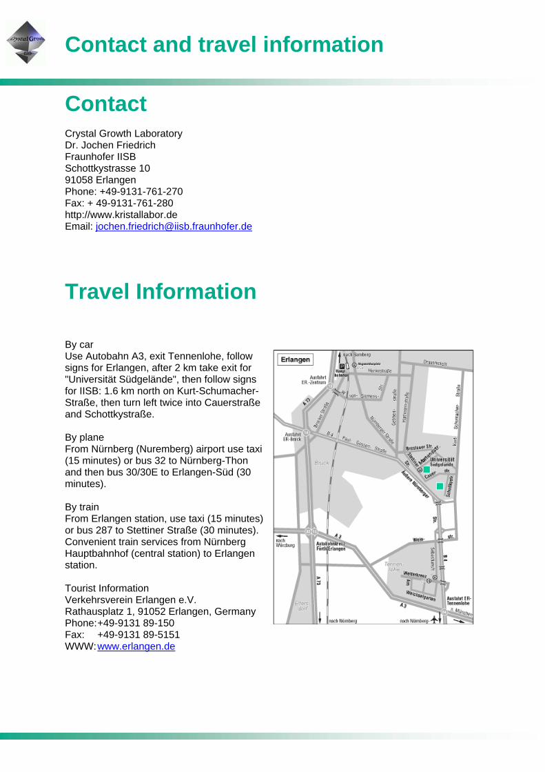
Travel Information By car Use Autobahn A3, exit Tennenlohe, follow signs for Erlangen, after 2 km take exit for "Universität Südgelände", then follow signs for IISB: 1.6 km north on Kurt-Schumacher-Straße, then turn left twice into Cauerstraße and Schottkystraße. By plane From Nürnberg (Nuremberg) airport use taxi (15 minutes) or bus 32 to Nürnberg-Thon and then bus 30/30E to Erlangen-Süd (30 minutes). By train From Erlangen station, use taxi (15 minutes) or bus 287 to Stettiner Straße (30 minutes). Convenient train services from Nürnberg Hauptbahnhof (central station) to Erlangen station. Tourist Information Verkehrsverein Erlangen e.V. Rathausplatz 1, 91052 Erlangen, Germany Phone: +49-9131 89-150 Fax: +49-9131 89-5151 WWW: www.erlangen.de
Crystal Growth Laboratory Dr. Jochen Friedrich Fraunhofer IISB Schottkystrasse 10 91058 Erlangen Phone: +49-9131-761-270 Fax: + 49-9131-761-280 http://www.kristallabor.de Email: [email protected]